
15
Inverters
Departamento de Ingeniería Eléctrica, of. 220, Universidad de Concepción, Casilla 160-C, Correo 3, Concepción, Chile
15.1 Introduction
15.2 Single-phase Voltage Source Inverters
15.2.1 Half-bridge VSI
15.2.2 Full-bridge VSI
15.3 Three-phase Voltage Source Inverters
15.3.1 Sinusoidal PWM
15.3.2 Square-wave Operation of Three-phase VSIs
15.3.3 Sinusoidal PWM with Zero Sequence Signal Injection
15.3.4 Selective Harmonic Elimination in Three-phase VSIs
15.3.5 Space-vector (SV)-based Modulating Techniques
15.4.1 Carrier-based PWM Techniques in CSIs
15.4.2 Square-wave Operation of Three-phase CSIs
15.4.3 Selective Harmonic Elimination in Three-phase CSIs
15.5 Closed-loop Operation of Inverters
15.5.1 Feedforward Techniques in Voltage Source Inverters
15.5.2 Feedforward Techniques in Current Source Inverters
15.6 Regeneration in Inverters
15.6.1 Motoring Operating Mode in Three-phase VSIs
15.7 Multistage Inverters
15.1 Introduction
The main objective of static power converters is to produce an ac output waveform from a dc power supply. These are the types of waveforms required in adjustable speed drives (ASDs), uninterruptible power supplies (UPSs), static var compensators, active filters, flexible ac transmission systems (FACTSs), and voltage compensators, which are only a few applications. For sinusoidal ac outputs, the magnitude, frequency, and phase should be controllable. According to the type of ac output waveform, these topologies can be considered as voltage-source inverters (VSIs), where the independently controlled ac output is a voltage waveform. These structures are the most widely used because they naturally behave as voltage sources as required by many industrial applications, such as ASDs, which are the most popular application of inverters (Fig. 15.1a). Similarly, these topologies can be found as current-source inverters (CSIs), where the independently controlled ac output is a current waveform. These structures are still widely used in medium-voltage industrial applications, where high-quality voltage waveforms are required.
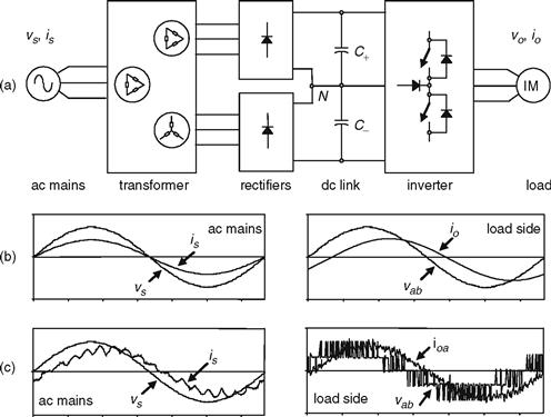
FIGURE 15.1 A three-level adjustable speed drive scheme and associated waveforms: (a) the electrical power conversion topology; (b) the ideal input (ac mains) and output (load) waveforms; and (c) the actual input (ac mains) and output (load) waveforms.
Static power converters, specifically inverters, are constructed from power switches and the ac output waveforms are therefore made up of discrete values. This leads to the generation of waveforms that feature fast transitions rather than smooth ones. For instance, the ac output voltage produced by the VSI of a three-level ASD is a, Pulse Width Modulation (PWM) type of waveform (Fig. 15.1c). Although this waveform is not sinusoidal as expected (Fig. 15.1b), its fundamental component behaves as such. This behavior should be ensured by a modulating technique that controls the amount of time and the sequence used to switch the power valves on and off. The modulating techniques most used are the carrier-based technique (e.g. sinusoidal pulsewidth modulation, SPWM), the space-vector (SV) technique, and the selective-harmonic-elimination (SHE) technique.
The discrete shape of the ac output waveforms generated by these topologies imposes basic restrictions on the applications of inverters. The VSI generates an ac output voltage waveform composed of discrete values (high dv/dt); therefore, the load should be inductive at the harmonic frequencies in order to produce a smooth current waveform. A capacitive load in the VSIs will generate large current spikes. If this is the case, an inductive filter between the VSI ac side and the load should be used. On the other hand, the CSI generates an ac output current waveform composed of discrete values (high di/dt); therefore, the load should be capacitive at the harmonic frequencies in order to produce a smooth voltage waveform. An inductive load in CSIs will generate large voltage spikes. If this is the case, a capacitive filter between the CSI ac side and the load should be used.
A three-level voltage waveform is not recommended for medium-voltage ASDs due to the high dv/dt that would apply to the motor terminals. Several negative side effects of this approach have been reported (bearing and isolation problems). As alternatives, to improve the ac output waveforms in VSIs are the multistage topologies (multilevel and multicell). The basic principle is to construct the required ac output waveform from various voltage levels, which achieves medium-voltage waveforms at reduced dv/dt. Although these topologies are well developed in ASDs, they are also suitable for static var compensators, active filters, and voltage compensators. Specialized modulating techniques have been developed to switch the higher number of power valves involved in these topologies. Among others, the carrier-based (SPWM) and SV-based techniques have been naturally extended to these applications.
In many applications, it is required to take energy from the ac side of the inverter and send it back into the dc side. For instance, whenever ASDs need to either brake or slow down the motor speed, the kinetic energy is sent into the voltage dc link (Fig. 15.1a). This is known as the regenerative operating mode and, in contrast to the motoring mode, the dc link current direction is reversed due to the fact that the dc link voltage is fixed. If a capacitor is used to maintain the dc link voltage (as in standard ASDs) the energy must either be dissipated or fed back into the distribution system, otherwise, the dc link voltage gradually increases. The first approach requires the dc link capacitor be connected in parallel with a resistor, which must be properly switched only when the energy flows from the motor into the dc link. A better alternative is to feed back such energy into the distribution system. However, this alternative requires a reversible-current topology connected between the distribution system and the dc link capacitor. A modern approach to such a requirement is to use the active front-end rectifier technologies, where the regeneration mode is a natural operating mode of the system.
In this chapter, single- and three-phase inverters in their voltage and current source alternatives will be reviewed. The dc link will be assumed to be a perfect dc, either voltage or current source that could be fixed as the dc link voltage in standard ASDs, or variable as the dc link current in some medium-voltage current source drives. Specifically, the topologies, modulating techniques and control aspects oriented to standard applications, are analyzed. In order to simplify the analysis, the inverters are considered lossless topologies, which are composed of ideal power valves. Nevertheless, some practical non-ideal conditions are also considered.
15.2 Single-phase Voltage Source Inverters
Single-phase VSI can be found as half-bridge and full-bridge topologies. Although, the power range they cover is the low one, they are widely used in power supplies, single-phase UPSs, and currently to form high-power static power topologies, such as the multicell configurations that are reviewed in Section 15.7. The main features of both approaches are reviewed and presented in the following.
15.2.1 Half-bridge VSI
Figure 15.2 shows the power topology of a half-bridge VSI, where two large capacitors are required to provide a neutral point N, such that each capacitor maintains a constant voltage vi2. Because the current harmonics injected by the operation of the inverter are low-order harmonics, a set of large capacitors (C+ and C_) is required. It is clear that both switches S+ and S_ cannot be on simultaneously because a short circuit across the dc link voltage source v, would be produced. There are two defined (states 1 and 2) and one undefined (state 3) switch state as shown in Table 15.1. In order to avoid the short circuit across the dc bus and the undefined ac output-voltage condition, the modulating technique should always ensure that at any instant either the top or the bottom switch of the inverter leg is on.
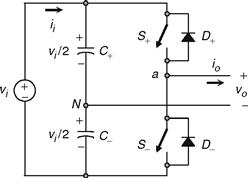
FIGURE 15.2 Single-phase half-bridge VSI.
TABLE 15.1 Switch states for a half-bridge single-phase VSI
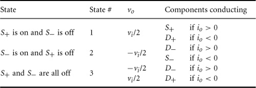
Figure 15.3 shows the ideal waveforms associated with the half-bridge inverter shown in Fig. 15.2. The states for the switches S+ and S_ are defined by the modulating technique, which in this case is a carrier-based PWM.
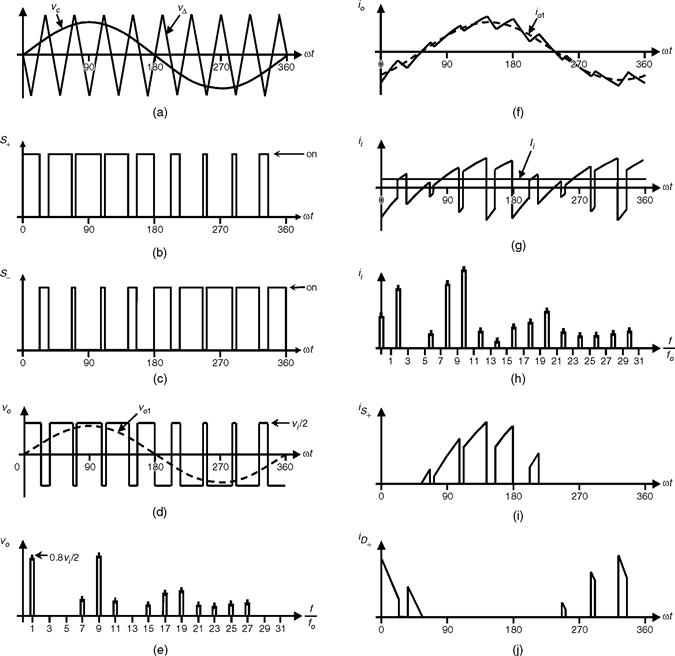
FIGURE 15.3 The half-bridge VSI. Ideal waveforms for the SPWM (ma = 0.8, mf = 9): (a) carrier and modulating signals; (b) switch S+ state; (c) switch S_ state; (d) ac output voltage; (e) ac output voltage spectrum; (f) ac output current; (g) dc current; (h) dc current spectrum; (i) switch S+ current; and (j) diode D+ current.
A. The Carrier-based Pulse Width Modulation (PWM) Technique
As mentioned earlier, it is desired that the ac output voltage, v0 = vaN, follow a given waveform (e.g. sinusoidal) on a continuous basis by properly switching the power valves. The carrier-based PWM technique fulfills such a requirement as it defines the on- and off-states of the switches of one leg of a VSI by comparing a modulating signal vc (desired ac output voltage) and a triangular waveform vΔ (carrier signal). In practice, when vΔ > vΔ the switch S+ is on and the switch S+ is off; similarly, when vc < vΔ the switch S+ is off and the switch S− is on.
A special case is when the modulating signal vc is a sinusoidal at frequency fc and amplitude ![]() and the triangular signal VΔ is at frequency fΔ and amplitude
and the triangular signal VΔ is at frequency fΔ and amplitude ![]() This is the sinusoidal PWM (SPWM) scheme. In this case, the modulation index ma (also known as the amplitude-modulation ratio) is defined as
This is the sinusoidal PWM (SPWM) scheme. In this case, the modulation index ma (also known as the amplitude-modulation ratio) is defined as
![]() (15.1)
(15.1)
and the normalized carrier frequency mf (also known as the frequency-modulation ratio) is
![]() (15.2)
(15.2)
Figure 15.3e clearly shows that the ac output voltage v0 = VaN is basically a sinusoidal waveform plus harmonics, which features: (a) the amplitude of the fundamental component of the ac output voltage ![]() satisfying the following expression:
satisfying the following expression:
![]() (15.3)
(15.3)
for ma ≤ 1, which is called the linear region of the modulating technique (higher values of ma leads to overmodulation that will be discussed later); (b) for odd values of the normalized carrier frequency mf the harmonics in the ac output voltage appear at normalized frequencies fh, centered around mf and its multiples, specifically,
![]() (15.4)
(15.4)
where k = 2,4,6,… for l = 1,3,5,…; and k = 1,3,5,… for l = 2, 4, 6,…; (c) the amplitude of the ac output voltage harmonics is a function of the modulation index ma and is independent of the normalized carrier frequency mf for mf > 9; (d) the harmonics in the dc link current (due to the modulation) appear at normalized frequencies fp centered around the normalized carrier frequency mf and its multiples, specifically,
![]() (15.5)
(15.5)
where k = 2,4,6,… for l = 1,3, 5,…; and k = 1,3, 5,… for l = 2,4,6,. …Additional important issues are: (a) for small values of mf (mf < 21), the carrier signal vΔ and the signal vc should be synchronized to each other (mf integer), which is required to hold the previous features; if this is not the case, subharmonics will be present in the ac output voltage; (b) for large values of mf (mf > 21), the subharmonics are negligible if an asynchronous PWM technique is used, however, due to potential very low-order subharmonics, its use should be avoided; finally (c) in the overmodulation region (ma > 1) some intersections between the carrier and the modulating signal are missed, which leads to the generation of low-order harmonics but a higher fundamental ac output voltage is obtained; unfortunately, the linearity between ma and ![]() achieved in the linear region does not hold in the overmodulation region, moreover, a saturation effect can be observed (Fig. 15.4).
achieved in the linear region does not hold in the overmodulation region, moreover, a saturation effect can be observed (Fig. 15.4).
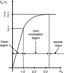
FIGURE 15.4 Normalized fundamental ac component of the output voltage in a half-bridge VSI SPWM modulated.
The PWM technique allows an ac output voltage to be generated that tracks a given modulating signal. A special case is the SPWM technique (the modulating signal is a sinusoidal) that provides, in the linear region, an ac output voltage that varies linearly as a function of the modulation index, and the harmonics are at well-defined frequencies and amplitudes. These features simplify the design of filtering components. Unfortunately, the maximum amplitude of the fundamental ac voltage is vi/2 in this operating mode. Higher voltages are obtained by using the overmodulation region (ma > 1); however, low-order harmonics appear in the ac output voltage. Very large values of the modulation index (ma > 3.24) lead to a totally square ac output voltage that is considered as the square-wave modulating technique.
B. Square-wave Modulating Technique
Both switches S+ and S_ are on for one half-cycle of the ac output period. This is equivalent to the SPWM technique with an infinite modulation index ma. Figure 15.5 shows the following: (a) the normalized ac output voltage harmonics are at frequencies h = 3, 5,7,9,…, and for a given dc link voltage; (b) the fundamental ac output voltage features an amplitude given by
![]() (15.6)
(15.6)
and the harmonics feature an amplitude given by
![]() (15.7)
(15.7)
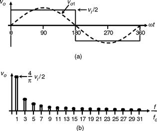
FIGURE 15.5 The half-bridge VSI. Ideal waveforms for the square-wave modulating technique: (a) ac output voltage and (b) ac output voltage spectrum.
It can be seen that the ac output voltage cannot be changed by the inverter. However, it could be changed by controlling the dc link voltage v. Other modulating techniques that are applicable to half-bridge configurations (e.g., selective harmonic elimination) are reviewed here as they can easily be extended to modulate other topologies.
C. Selective Harmonic Elimination
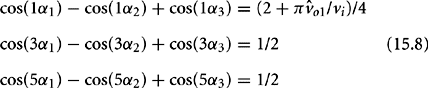
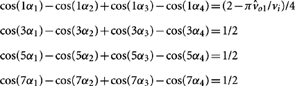
The main objective is to obtain a sinusoidal ac output voltage waveform where the fundamental component can be adjusted arbitrarily within a range and the intrinsic harmonics selectively eliminated. This is achieved by mathematically generating the exact instant of the turn-on and turn-off of the power valves. The ac output voltage features odd half-and quarter-wave symmetry; therefore, even harmonics are not present ![]() . Moreover, the phase voltage waveform (vo = vaN in Fig. 15.2), should be chopped N times per half-cycle in order to adjust the fundamental and eliminate N − 1 harmonics in the ac output voltage waveform. For instance, to eliminate the third and fifth harmonics and to perform fundamental magnitude control (N = 3), the equations to be solved are the following:
. Moreover, the phase voltage waveform (vo = vaN in Fig. 15.2), should be chopped N times per half-cycle in order to adjust the fundamental and eliminate N − 1 harmonics in the ac output voltage waveform. For instance, to eliminate the third and fifth harmonics and to perform fundamental magnitude control (N = 3), the equations to be solved are the following:
 (15.8)
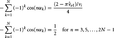
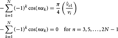
where the angles α1, α2 and α3 are defined as shown in Fig. 15.6a. The angles are found by means of iterative algorithms as no analytical solutions can be derived. The angles a α1, α2, and α3 are plotted for different values of ![]() in Fig. 15.7a. The general expressions to eliminate an even N − 1 (N − 1 = 2,4,6,…) number of harmonics are
in Fig. 15.7a. The general expressions to eliminate an even N − 1 (N − 1 = 2,4,6,…) number of harmonics are
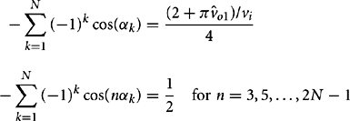 (15.9)
where α1, α2. …, αN should satisfy α1 < α2 < … < αN < π/2. Similarly, to eliminate an odd number of harmonics, for instance the third, fifth, and seventh, and to perform the fundamental magnitude control (N − 1 = 3), the equations to be solved are:
 (15.10)
where the angles α1, α2, α3, and α4 are defined as shown in Fig. 15.6b. The angles α1, α2., and α3 are plotted for different values of ![]() in Fig. 15.7b. The general expressions to eliminate an odd N − 1 (N − 1 = 3,5,7,…) number of harmonics are given by
in Fig. 15.7b. The general expressions to eliminate an odd N − 1 (N − 1 = 3,5,7,…) number of harmonics are given by
 (15.11)
where α1, α2, … αN should satisfy α1 < α2 < … < αN < π/2.
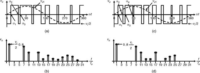
FIGURE 15.6 The half-bridge VSI. Ideal waveforms for the SHE technique: (a) ac output voltage for third and fifth harmonic elimination; (b) spectrum of (a); (c) ac output voltage for third, fifth, and seventh harmonic elimination; and (d) spectrum of (c).
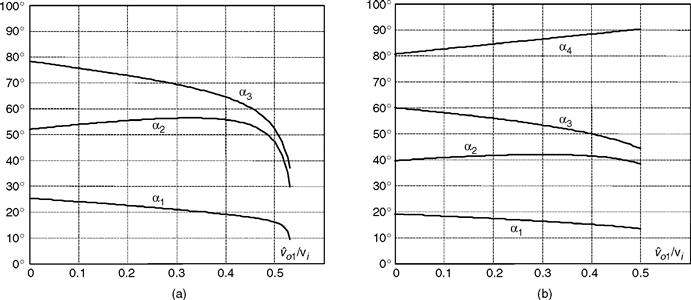
FIGURE 15.7 Chopping angles for SHE and fundamental voltage control in half-bridge VSIs: (a) third and fifth harmonic elimination and (b) third, fifth, and seventh harmonic elimination.
To implement the SHE modulating technique, the modulator should generate the gating pattern according to the angles as shown in Fig. 15.7. This task is usually performed by digital systems that normally store the angles in look-up tables.
D. DC Link Current
The split capacitors are considered a part of the inverter and therefore an instantaneous power balance cannot be considered due to the storage energy components (C+ and C_). However, if a lossless inverter is assumed, the average power absorbed in one period by the load must be equal to the average power supplied by the dc source. Thus, we can write
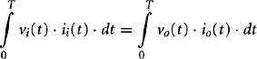 (15.12)
where T is the period of the ac output voltage. For an inductive load and a relatively high switching frequency, the load current i0 is nearly sinusoidal and therefore, only the fundamental component of the ac output voltage provides power to the load. On the other hand, if the dc link voltage remains constant Vi(t) = Vi, Eq. (15.12) can be simplified to
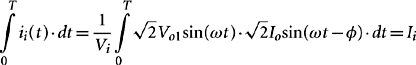 (15.13)
where V01 is the fundamental rms ac output voltage, I0 is the rms load current, ϕ is an arbitrary inductive load power factor, and Ii is the dc link current that can be further simplified to
![]() (15.14)
(15.14)
15.2.2 Full-bridge VSI
Figure 15.8 shows the power topology of a full-bridge VSI. This inverter is similar to the half-bridge inverter; however, a second leg provides the neutral point to the load. As expected, both switches S1+ and S1- (or S2+ and S2−) cannot be on simultaneously because a short circuit across the dc link voltage source vi would be produced. There are four defined (states 1, 2, 3, and 4) and one undefined (state 5) switch state as shown in Table 15.2.
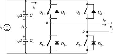
FIGURE 15.8 Single-phase full-bridge VSI.
TABLE 15.2 Switch states for a full-bridge single-phase VSI
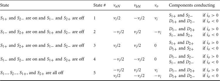
The undefined condition should be avoided so as to be always capable of defining the ac output voltage always. In order to avoid the short circuit across the dc bus and the undefined ac output voltage condition, the modulating technique should ensure that either the top or the bottom switch of each leg is on at any instant. It can be observed that the ac output voltage can take values up to the dc link value vi, which is twice that obtained with half-bridge VSI topologies.
Several modulating techniques have been developed that are applicable to full-bridge VSIs. Among them are the PWM (bipolar and unipolar) techniques.
A. Bipolar PWM Technique
States 1 and 2 (Table 15.2) are used to generate the ac output voltage in this approach. Thus, the ac output voltage waveform features only two values, which are vi and — vi. To generate the states, a carrier-based technique can be used as in half-bridge configurations (Fig. 15.3), where only one sinusoidal modulating signal has been used. It should be noted that the on-state in switch S+ in the half-bridge corresponds to both switches S1+ and S2− being in the on-state in the full-bridge configuration. Similarly, S_ in the on-state in the half-bridge corresponds to both switches S1+ and S2− being in the on-state in the full-bridge configuration. This is called bipolar carrier-based SPWM. The ac output voltage waveform in a full-bridge VSI is basically a sinusoidal waveform that features a fundamental component of amplitude ![]() that satisfies the expression
that satisfies the expression
![]() (15.15)
(15.15)
in the linear region of the modulating technique (ma ≤ 1), which is twice that obtained in the half-bridge VSI. Identical conclusions can be drawn for the frequencies and the amplitudes of the harmonics in the ac output voltage and dc link current, and for operations at smaller and larger values of odd mf (including the overmodulation region (ma > 1)), than in half-bridge VSIs, but considering that the maximum ac output voltage is the dc link voltage vi. Thus, in the over-modulation region the fundamental component of amplitude ![]() satisfies the expression
satisfies the expression
![]() (15.16)
(15.16)
B. Unipolar PWM Technique
In contrast to the bipolar approach, the unipolar PWM technique uses the states 1, 2, 3, and 4 (Table 15.2) to generate the ac output voltage. Thus, the ac output voltage waveform can instantaneously take one of the three values, namely vi, −vi, and 0. To generate the states, a carrier-based technique can be used as shown in Fig. 15.9, where two sinusoidal modulating signals (vc and — vc) are used. The signal vc is used to generate vaN, and — vc is used to generate vbn; thus vbn1 = vaN1- On the other hand, v01 = vaN1 –vbN1,= 2. vaN1; thus ![]() This is called unipolar carrier-based SPWM.
This is called unipolar carrier-based SPWM.
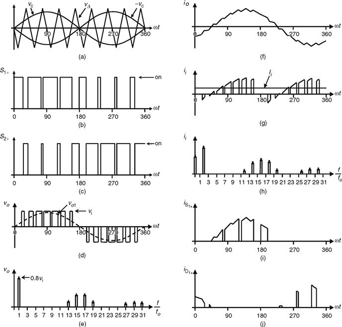
FIGURE 15.9 The fall-bridge VSI. Ideal waveforms for the unipolar SPWM (ma = 0.8, mf = 8): (a) carrier and modulating signals; (b) switch Si+ state; (c) switch S2+ state; (d) ac output voltage; (e) ac output voltage spectrum; (f) ac output current; (g) de current; (h) de current spectrum; (i) switch S14. current; and (j) diode D1+ current.
Identical conclusions can be drawn for the amplitude of the fundamental component and harmonics in the ac output voltage and dc link current, and for operations at smaller and larger values of mf (including the overmodulation region (ma > 1)) than in full-bridge VSIs modulated by the bipolar SPWM. However, because the phase voltages (vnN and vbN) are identical but 180° out of phase, the output voltage (vo = vab = vaN − vbn) will not contain even harmonics. Thus, if mf is taken even, the harmonics in the ac output voltage appear at normalized odd frequencies fh centered around twice the normalized carrier frequency mf and its multiples. Specifically,
![]() (15.17)
(15.17)
where k = 1,3, 5,… and the harmonics in the dc link current appear at normalized frequencies fp centered around twice the normalized carrier frequency mf and its multiples. Specifically,
![]() (15.18)
(15.18)
where k = 1,3, 5,… This feature is considered to be an advantage because it allows the use of smaller filtering components to obtain high-quality voltage and current waveforms while using the same switching frequency as in VSIs modulated by the bipolar approach.
C. Selective Harmonic Elimination
In contrast to half-bridge VSIs, this approach is applied in a per-line fashion for full-bridge VSIs. The ac output voltage features odd half- and quarter-wave symmetry; therefore, even harmonics are not present ![]() . Moreover, the ac output voltage waveform (v0 = vfl in Fig. 15.8), should feature N pulses per half-cycle in order to adjust the fundamental component and eliminate N − 1 harmonics. For instance, to eliminate the third, fifth, and the seventh harmonics and to perform fundamental component magnitude control (N = 4), the equations to be solved are:
. Moreover, the ac output voltage waveform (v0 = vfl in Fig. 15.8), should feature N pulses per half-cycle in order to adjust the fundamental component and eliminate N − 1 harmonics. For instance, to eliminate the third, fifth, and the seventh harmonics and to perform fundamental component magnitude control (N = 4), the equations to be solved are:
 (15.19)
where the angles α1, α2, α3, and α4, are defined as shown in Fig. 15.10a. The angles α1, α2, α3, and α4, are plotted for different values of ![]() in Fig. 15.11a. The general expressions to eliminate an arbitrary N — I (N − 1 = 3, 5,7,…) number of harmonics are given by
in Fig. 15.11a. The general expressions to eliminate an arbitrary N — I (N − 1 = 3, 5,7,…) number of harmonics are given by
 (15.20)
where α1, α2 …, αN should satisfy α1 < α2 < … < αN < ϕ/2.

FIGURE 15.10 The half-bridge VSI. Ideal waveforms for the SHE technique: (a) ac output voltage for third, fifth, and seventh harmonic elimination; (b) spectrum of (a); (c) ac output voltage for fundamental control; and (d) spectrum of (c).
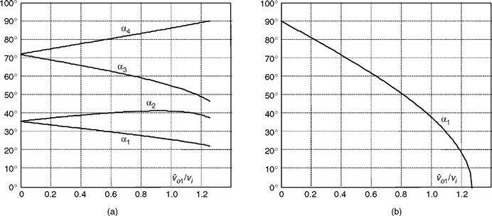
FIGURE 15.11 Chopping angles for SHE and fundamental voltage control in half-bridge VSIs: (a) fundamental control and third, fifth, and seventh harmonic elimination and (b) fundamental control.
Figure 15.10c shows a special case where only the fundamental ac output voltage is controlled. This is known as output control by voltage cancellation, which derives from the fact that its implementation is easily attainable by using two phase-shifted square-wave switching signals as shown in Fig. 15.12. The phase-shift angle becomes 2 α1 (Fig. 15.11b). Thus, the amplitude of the fundamental component and harmonics in the ac output voltage are given by
![]() (15.21)
(15.21)
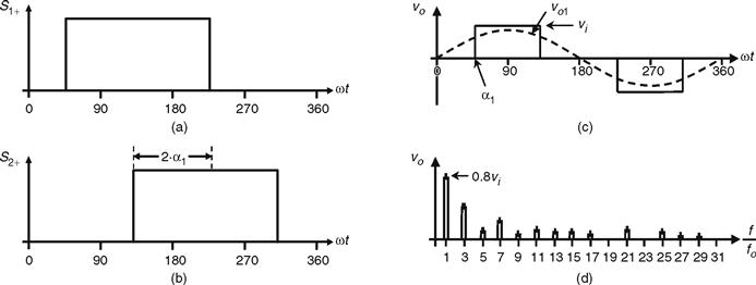
FIGURE 15.12 The fall-bridge VSI. Ideal waveforms for the output control by voltage cancellation: (a) switch S1+. state; (b) switch S2+ state; (c) ac output voltage; and (d) ac output voltage spectrum.
It can also be observed in Fig. 15.12c that for α1 = 0 square-wave operation is achieved. In this case, the fundamental
ac output voltage is given by
![]() (15.22)
(15.22)
where the fundamental load voltage can be controlled by the manipulation of the dc link voltage.
D. DC Link Current
Due to the fact that the inverter is assumed lossless and constructed without storage energy components, the instantaneous power balance indicates that,
![]() (15.23)
(15.23)
For inductive load and relatively high switching frequencies, the load current i0 is nearly sinusoidal. As a first approximation, the ac output voltage can also be considered sinusoidal. On the other hand, if the dc link voltage remains constant Vi(t) = Vi, Eq. (15.23) can be simplified to
![]() (15.24)
(15.24)
where V01 is the fundamental rms ac output voltage, I0 is the rms load current, and ϕ is an arbitrary inductive load power factor. Thus, the dc link current can be further simplified to
![]() (15.25)
(15.25)
The preceding expression reveals an important issue, that is, the presence of a large second-order harmonic in the dc link current (its amplitude is similar to the dc link current). This second harmonic is injected back into the dc voltage source, thus its design should consider it in order to guarantee a nearly constant dc link voltage. In practical terms, the dc voltage source is required to feature large amounts of capacitance, which is costly and demands space, both undesired features, especially in medium- to high-power supplies.
15.3 Three-phase Voltage Source Inverters
Single-phase VSIs cover low-range power applications and three-phase VSIs cover medium- to high-power applications. The main purpose of these topologies is to provide a three-phase voltage source, where the amplitude, phase, and frequency of the voltages should always be controllable. Although most of the applications require sinusoidal voltage waveforms (e.g. ASDs, UPSs, FACTS, var compensators), arbitrary voltages are also required in some emerging applications (e.g. active filters, voltage compensators).
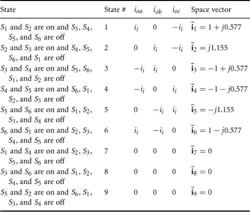
The standard three-phase VSI topology is shown in Fig. 15.13 and the eight valid switch states are given in Table 15.3. As in single-phase VSIs, the switches of any leg of the inverter (S1 and S4, S3 and S6, or S5 and S2) cannot be switched on simultaneously because this would result in a short circuit across the dc link voltage supply. Similarly, in order to avoid undefined states in the VSI, and thus undefined ac output line voltages, the switches of any leg of the inverter cannot be switched off simultaneously as this will result in voltages that will depend upon the respective line current polarity.
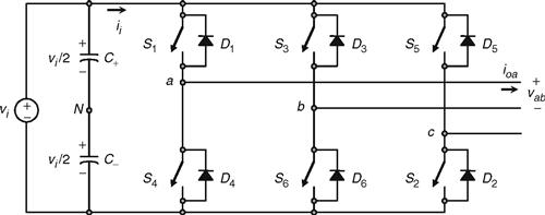
FIGURE 15.13 Three-phase VSI topology.
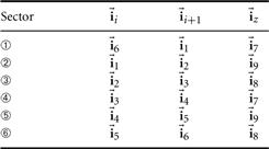
TABLE 15.3 Valid switch states for a three-phase VSI
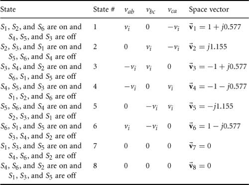
Of the eight valid states, two of them (7 and 8 in Table 15.3) produce zero ac line voltages. In this case, the ac line currents freewheel through either the upper or lower components. The remaining states (1 to 6 in Table 15.3) produce non-zero ac output voltages. In order to generate a given voltage waveform, the inverter moves from one state to another. Thus the resulting ac output line voltages consist of discrete values of voltages that are vi, 0, and −v, for the topology shown in Fig. 15.13. The selection of the states in order to generate the given waveform is done by the modulating technique that should ensure the use of only the valid states.
15.3.1 Sinusoidal PWM
This is an extension of the one introduced for single-phase VSIs. In this case and in order to produce 120° out-of-phase load voltages, three modulating signals that are 120° out-of-phase are used. Figure 15.14 shows the ideal waveforms of three-phase VSI SPWM. In order to use a single carrier signal and preserve the features of the PWM technique, the normalized carrier frequency mf should be an odd multiple of 3. Thus, all phase voltages (vaN, VbN, and vcN) are identical, but 120° out-of-phase without even harmonics; moreover, harmonics at frequencies, a multiple of 3, are identical in amplitude and phase in all phases. For instance, if the ninth harmonic in phase aN is
![]() (15.26)
(15.26)
the ninth harmonic in phase bN will be
 (15.27)
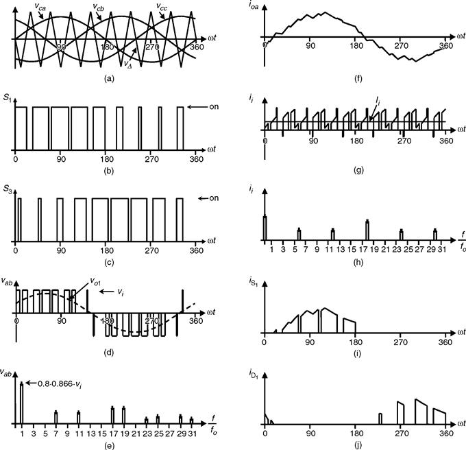
FIGURE 15.14 The three-phase VSI. Ideal waveforms for the SPWM (ma = 0.8, mf = 9): (a) carrier and modulating signals; (b) switch Si state; (c) switch S3 state; (d) ac output voltage; (e) ac output voltage spectrum; (f) ac output current; (g) de current; (h) de current spectrum; (i) switch Si current; and (j) diode D1 current.
Thus, the ac output line voltage vab = vaN — VbN will not contain the ninth harmonic. Therefore, for odd multiple of 3 values of the normalized carrier frequency mf, the harmonics in the ac output voltage appear at normalized frequencies fh, centered around mf and its multiples, specifically, at
![]() (15.28)
(15.28)
where l = 1,3,5,… for k = 2,4,6,… and I = 2,4,… for k = 1, 5,7,… such that h is not a multiple of 3. Therefore, the harmonics will be at ± 2, mf = b 4,…, 2 mf ± 1, 2 mf ± 5,…, 3 mf ± 2, 3 mf ± 4,…, 4 mf ± 1, 4 mf ± 5,__For nearly sinusoidal ac load current, the harmonics in the dc link current are at frequencies given by
![]() (15.29)
(15.29)
where l = 0,2,4,… for k = 1,5,7,… and l = 1,3,5,… for k = 2,4,6,… such that h = I (mf ± k is positive and not a multiple of 3. For instance, Fig. 15.14h shows the sixth harmonic (h = 6), which is due to h = 1 9 − 2 − 1 = 6.
The identical conclusions can be drawn for the operation at small and large values of mf as for the single-phase configurations. However, because the maximum amplitude of the fundamental phase voltage in the linear region (ma ≤ 1) is vi/2, the maximum amplitude of the fundamental ac output line voltage is (3vi,/2. Therefore, one can write
![]() (15.30)
(15.30)
To further increase the amplitude of the load voltage, the amplitude of the modulating signal ![]() can be made higher than the amplitude of the carrier signal
can be made higher than the amplitude of the carrier signal ![]() , which leads to overmodulation. The relationship between the amplitude of the fundamental ac output line voltage and the dc link voltage becomes non-linear as in single-phase VSIs. Thus, in the overmodulation region, the line voltages range is
, which leads to overmodulation. The relationship between the amplitude of the fundamental ac output line voltage and the dc link voltage becomes non-linear as in single-phase VSIs. Thus, in the overmodulation region, the line voltages range is
![]() (15.31)
(15.31)
15.3.2 Square-wave Operation of Three-phase VSIs
Large values of ma in the SPWM technique lead to full overmodulation. This is known as square-wave operation as illustrated in Fig. 15.15, where the power valves are on for 180°.
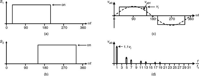
FIGURE 15.15 The three-phase VSI. Square-wave operation: (a) switch Si state; (b) switch S3 state; (c) ac output voltage; and (d) ac output voltage spectrum.
In this operation mode, the VSI cannot control the load voltage except by means of the dc link voltage vi. This is based on the fundamental ac line-voltage expression
![]() (15.32)
(15.32)
The ac line output voltage contains the harmonics fh, where h = 6 k = 1 (k = 1,2,3,…) and they feature amplitudes that are inversely proportional to their harmonic order (Fig. 15.15d). Their amplitudes are
![]() (15.33)
(15.33)
15.3.3 Sinusoidal PWM with Zero Sequence Signal Injection
The restriction for ma (ma ≤ 1) can be relaxed if a zero sequence signal is added to the modulating signals before they are compared to the carrier signal. Figure 15.16 shows the block diagram of the technique. Clearly, the addition of the zero sequence reduces the peak amplitude of the resulting modulating signals (uca, ucb, ucc), while the fundamental components remain unchanged. This approach expands the range of the linear region as it allows the use of modulation indexes ma up to ![]() without getting into the overmodulating region.
without getting into the overmodulating region.

FIGURE 15.16 Zero sequence signal generator (ma = 1.0, mf = 9): (a) block diagram; (b) modulating signals; and (c) zero sequence and modulating signals with zero sequence injection.
The maximum amplitude of the fundamental phase voltage in the linear region (ma ≤ ![]() ) is vi,/2, thus, the maximum amplitude of the fundamental ac output line voltage is vi. Therefore, one can write
) is vi,/2, thus, the maximum amplitude of the fundamental ac output line voltage is vi. Therefore, one can write
![]() (15.34)
(15.34)
Figure 15.17 shows the ideal waveforms of a three-phase VSI SPWM with zero injection for ma = 0.8.
FIGURE 15.17 The three-phase VSI. Ideal waveforms for the SPWM (ma = 0.8, mf = 9) with zero sequence signal injection: (a) modulating signals; (b) carrier and modulating signals with zero sequence signal injection; (c) switch Si state; (d) ac output voltage; (e) ac output voltage spectrum; (f) ac output current; (g) dc current; (h) de current spectrum; (i) switch Si current; and (j) diode Di current.
15.3.4 Selective Harmonic Elimination in Three-phase VSIs
As in single-phase VSIs, the SHE technique can be applied to three-phase VSIs. In this case, the power valves of each leg of the inverter are switched so as to eliminate a given number of harmonics and to control the fundamental phase-voltage amplitude. Considering that in many applications, the required line output voltages should be balanced and 120° out of phase, the harmonics multiples of 3 (h = 3,9, 15,…), which could be present in the phase voltages (vaN, VbN, and vcn), will not be present in the load voltages (vab, VbC, and vca). Therefore, these harmonics are not required to be eliminated, thus the chopping angles are used to eliminate only the harmonics at frequencies h = 5,7,11,13,… as required.
The expressions to eliminate a given number of harmonics are the same as those used in single-phase inverters. For instance, to eliminate the fifth and seventh harmonics and perform fundamental magnitude control (N = 3), the equations to be solved are:
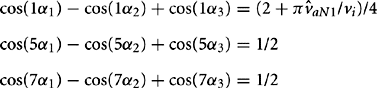 (15.35)
where the angles α1, α2, and α3 are defined as shown in Fig. 15.18a and plotted in Fig. 15.19. Figure 15.18b shows that the third, ninth, fifteenth, … harmonics are all present in the phase voltages; however, they are not in the line voltages (Fig. 15.18d).

FIGURE 15.18 The three-phase VSI. Ideal waveforms for the SHE technique: (a) phase voltage vaN for fifth and seventh harmonic elimination; (b) spectrum of (a); (c) line voltage vab, for fifth and seventh harmonic elimination; and (d) spectrum of (c).
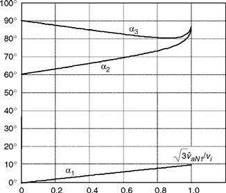
FIGURE 15.19 Chopping angles for SHE and fundamental voltage control in three-phase VSIs: fifth and seventh harmonic elimination.
15.3.5 Space-vector (SV)-based Modulating Techniques
At present, the control strategies are implemented in digital systems, and therefore digital modulating techniques are also available. The SV-based modulating technique is a digital technique in which the objective is to generate PWM load line voltages that are on average equal to given load line voltages. This is done in each sampling period by properly selecting the switch states from the valid ones of the VSI (Table 15.3) and by proper calculation of the period of times they are used. The selection and calculation times are based upon the SV transformation.
A. Space-vector Transformation
Any three-phase set of variables that add up to zero in the stationary abc frame can be represented in a complex plane by a complex vector that contains a real (a) and an imaginary (β) component. For instance, the vector of three-phase line-modulating signals vcabc = [vcavcbVcc]T can be represented by the complex vector ![]() by means of the following transformation:
by means of the following transformation:
![]() (15.36)
(15.36)
![]() (15.37)
(15.37)
If the line-modulating signals vcabc are three balanced sinusoidal waveforms that feature an amplitude ![]() and an angular frequency ω, the resulting modulating signals in the αβ stationary frame become a vector
and an angular frequency ω, the resulting modulating signals in the αβ stationary frame become a vector ![]() of fixed module
of fixed module ![]() which rotates at frequency ω (Fig. 15.20). Similarly, the SV transformation is applied to the line voltages of the eight states of the VSI normalized with respect to vi, (Table 15.3), which generates the eight space vectors (
which rotates at frequency ω (Fig. 15.20). Similarly, the SV transformation is applied to the line voltages of the eight states of the VSI normalized with respect to vi, (Table 15.3), which generates the eight space vectors (![]() i = 1,2,…, 8) in Fig. 15.20. As expected,
i = 1,2,…, 8) in Fig. 15.20. As expected, ![]() to
to ![]() are non-null line-voltage vectors and
are non-null line-voltage vectors and ![]() and
and ![]() are null line-voltage vectors.
are null line-voltage vectors.
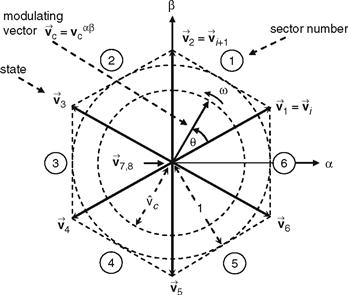
FIGURE 15.20 The space-vector representation.
The objective of the SV technique is to approximate the line-modulating signal space vector ![]() with the eight space vectors (
with the eight space vectors (![]() i = 1,2,…, 8) available in VSIs. However, if the modulating signal
i = 1,2,…, 8) available in VSIs. However, if the modulating signal ![]() is laying between the arbitrary vectors
is laying between the arbitrary vectors ![]() , and
, and ![]() , only the nearest two non-zero vectors (
, only the nearest two non-zero vectors (![]() and
and ![]() ) and one zero SV
) and one zero SV ![]() should be used. Thus, the maximum load line voltage is maximized and the switching frequency is minimized. To ensure that the generated voltage in one sampling period Ts (made up of the voltages provided by the vectors
should be used. Thus, the maximum load line voltage is maximized and the switching frequency is minimized. To ensure that the generated voltage in one sampling period Ts (made up of the voltages provided by the vectors ![]() and
and ![]() used during times Ti, Ti+ 1, and Tz) is on average equal to the vector
used during times Ti, Ti+ 1, and Tz) is on average equal to the vector ![]() the following expression should hold:
the following expression should hold:
![]() (15.38)
(15.38)
The solution of the real and imaginary parts of Eq. (15.37) for a line-load voltage that features an amplitude restricted to 0 ≤ ![]() 1 ≤ gives
1 ≤ gives
![]() (15.39)
(15.39)
![]() (15.40)
(15.40)
![]() (15.41)
(15.41)
The preceding expressions indicate that the maximum fundamental line-voltage amplitude is unity as 0 ≤ 0 ≤ ϕ/3. This is an advantage over the SPWM technique which achieves a √ 3/2 maximum fundamental line-voltage amplitude in the linear operating region. Although, the space vector modulation (SVM) technique selects the vectors to be used and their respective on-times, the sequence in which they are used, the selection of the zero space vector, and the normalized sampled frequency remain undetermined.
For instance, if the modulating line-voltage vector is in sector 1 (Fig. 15.20), the vectors ![]() ,
, ![]() , and
, and ![]() should be used within a sampling period by intervals given by T1, T2, and Tz, respectively. The question that remains is whether the sequence (i)
should be used within a sampling period by intervals given by T1, T2, and Tz, respectively. The question that remains is whether the sequence (i) ![]() -
- ![]() -
- ![]() , (ii)
, (ii)![]() -
- ![]() -
- ![]() -
- ![]() (iii)
(iii)![]() -
- ![]() -
- ![]() -
- ![]() -
- ![]() . (iv)
. (iv) ![]() -
- ![]() -
- ![]() -
- ![]() -
- ![]() , -
, - ![]() -
- ![]() or any other sequence should actually be used. Finally, the technique does not indicate whether
or any other sequence should actually be used. Finally, the technique does not indicate whether ![]() should be
should be ![]() ,
, ![]() , or a combination of both.
, or a combination of both.
B. Space-vector Sequences and Zero Space-vector Selection
The sequence to be used should ensure load line-voltages that feature quarter-wave symmetry in order to reduce unwanted harmonics in their spectra (even harmonics). Additionally, the zero SV selection should be done in order to reduce the switching frequency. Although there is not a systematic approach to generate a SV sequence, a graphical representation shows that the sequence ![]()
![]()
![]() (where
(where ![]() is alternately chosen among
is alternately chosen among ![]() and
and ![]() ) provides high performance in terms of minimizing unwanted harmonics and reducing the switching frequency.
) provides high performance in terms of minimizing unwanted harmonics and reducing the switching frequency.
C. The Normalized Sampling Frequency
The normalized carrier frequency mf in three-phase carrier-based PWM techniques is chosen to be an odd integer number multiple of 3 (mf = 3 n, n = 1,3, 5,…). Thus, it is possible to minimize parasitic or non-intrinsic harmonics in the PWM waveforms. A similar approach can be used in the SVM technique to minimize uncharacteristic harmonics. Hence, it is found that the normalized sampling frequency fsn should be an integer multiple of 6. This is due to the fact that in order to produce symmetrical line voltages, all the sectors (a total of 6) should be used equally in one period. As an example, Fig. 15.21 shows the relevant waveforms of a VSI SVM for fsn = 18 and vc = 0.8. Figure 15.21 confirms that the first set of relevant harmonics in the load line voltage are at fsn which is also the switching frequency.
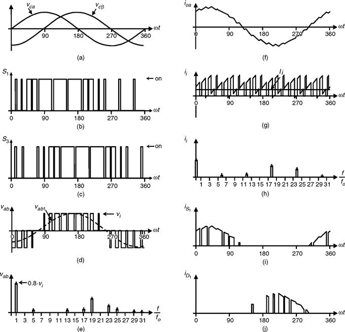
FIGURE 15.21 The three-phase VSI. Ideal waveforms for space-vector modulation ![]() : (a) modulating signals; (b) switch Si state; (c) switch S3 state; (d) ac output voltage; (e) ac output voltage spectrum; (f) ac output current; (g) de current; (h) de current spectrum; (i) switch Si current; and (j) diode D1 current.
: (a) modulating signals; (b) switch Si state; (c) switch S3 state; (d) ac output voltage; (e) ac output voltage spectrum; (f) ac output current; (g) de current; (h) de current spectrum; (i) switch Si current; and (j) diode D1 current.
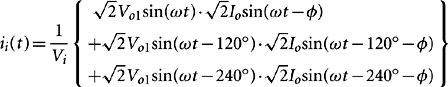
15.3.6 DC Link Current in Three-phase VSIs
Due to the fact that the inverter is assumed to be lossless and constructed without storage energy components, the instantaneous power balance indicates that
![]() (15.42)
(15.42)
where ia(t), ib(t), and ic(t) are the phase-load currents as shown in Fig. 15.22. If the load is balanced and inductive, and a relatively high switching frequency is used, the load currents become nearly sinusoidal balanced waveforms. On the other hand, if the ac output voltages are considered sinusoidal and the dc link voltage is assumed constant v,(t) = Vi, Eq. (15.42) can be simplified to
 (15.43)
where V01 is the fundamental rms ac output line voltage, I0 is the rms load-phase current, and f is an arbitrary inductive load power factor. Hence, the dc link current expression can be further simplified to
![]() (15.44)
(15.44)
where Il = ![]() is the rms load line current. The resulting dc link current expression indicates that under harmonic-free load voltages, only a clean dc current should be expected in the dc bus and, compared to single-phase VSIs, there is no presence of second harmonic. However, as the ac load line voltages contain harmonics around the normalized sampling frequency fsn, the dc link current will contain harmonics but around fsn as shown in Fig. 15.21h.
is the rms load line current. The resulting dc link current expression indicates that under harmonic-free load voltages, only a clean dc current should be expected in the dc bus and, compared to single-phase VSIs, there is no presence of second harmonic. However, as the ac load line voltages contain harmonics around the normalized sampling frequency fsn, the dc link current will contain harmonics but around fsn as shown in Fig. 15.21h.
FIGURE 15.22 Phase-load currents definition in a delta-connected load.
15.3.7 Load-phase Voltages in Three-phase VSIs
The load is sometimes wye-connected and the phase-load voltages van, vbn, and vcn maybe required (Fig. 15.23). To obtain them, it should be considered that the line-voltage vector is
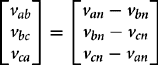 (15.45)
which can be written as a function of the phase-voltage vector [Van Vbn Vcn]T as
 (15.46)

FIGURE 15.23 Phase-load voltages definition in a wye-connected load.
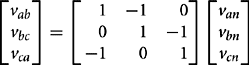
Expression (15.46) represents a linear system where the unknown quantity is the vector [vanVbnVcn]T. Unfortunately, thev system is singular as the rows add up to zero (line voltages add up to zero), therefore, the phase-load voltages cannot be obtained by matrix inversion. However, if the phase-load voltages add up to zero, Eq. (15.46) can be rewritten as
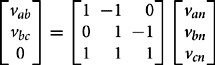 (15.47)
which is not singular and hence,
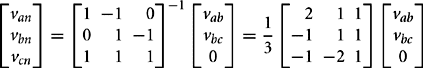 (15.48)
that can be further simplified to
 (15.49)
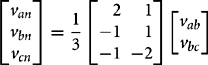
The final expression for the phase-load voltages is only a function of vab and vbc, which is due to fact that the last row in Eq. (15.46) is chosen to be only ones. Figure 15.24 shows the line- and phase-voltages obtained using Eq. (15.49).
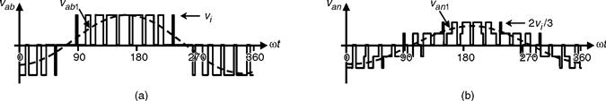
FIGURE 15.24 The three-phase VSI. Line- and phase-load voltages: (a) line-load voltage vab; and (b) phase-load voltage van.
15.4 Current Source Inverters
The main objective of these static power converters is to produce an ac output current waveforms from a dc current power supply. For sinusoidal ac outputs, its magnitude, frequency, and phase should be controllable. Due to the fact that the ac line currents ioa, i0b, and ioc (Fig. 15.25) feature high di/dt, a capacitive filter should be connected at the ac terminals in inductive load applications (such as ASDs). Thus, nearly sinusoidal load voltages are generated that justifies the use of these topologies in medium-voltage industrial applications, where high-quality voltage waveforms are required. Although single-phase CSIs can in the same way as three-phase CSIs topologies, be developed under similar principles, only three-phase applications are of practical use and are analyzed below.
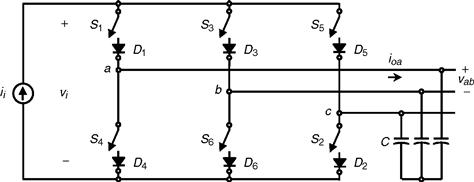
FIGURE 15.25 Three-phase CSI topology.
In order to properly gate the power switches of a three-phase CSI, two main constraints must always be met: (a) the ac side is mainly capacitive, thus, it must not be short-circuited; this implies that, at most one top switch (1, 3, or 5 (Fig. 15.25)) and one bottom switch (4, 6, or 2 (Fig. 15.25)) should be closed at any time; and (b) the dc bus is of the current-source type and thus it cannot be opened; therefore, there must be at least one top switch (1,3, or 5) and one bottom switch (4, 6, or 2) closed at all times. Note that both constraints can be summarized by stating that at any time, only one top switch and one bottom switch must be closed.
There are nine valid states in three-phase CSIs. The states 7, 8, and 9 (Table 15.4) produce zero ac line currents. In this case, the dc link current freewheels through either the switches S1 and S4, switches S3 and S6, or switches S5 and S2. The remaining states (1 to 6 in Table 15.4) produce non-zero ac output line currents. In order to generate a given set of ac line current waveforms, the inverter must move from one state to another. Thus, the resulting line currents consist of discrete values of current, which are ii, 0, and − ii. The selection of the states in order to generate the given waveforms is done by the modulating technique that should ensure the use of only the valid states.
TABLE 15.4 Valid switch states for a three-phase CSI
There are several modulating techniques that deal with the special requirements of CSIs and can be implemented online. These techniques are classified into three categories: (a) the carrier-based; (b) the SHE-based; and (c) the SV-based techniques. Although they are different, they generate gating signals that satisfy the special requirements of CSIs. To simplify the analysis, a constant dc link-current source is considered (ii = Ii).
15.4.1 Carrier-based PWM Techniques in CSIs
It has been shown that the carrier-based PWM techniques that were initially developed for three-phase VSIs can be extended to three-phase CSIs. The circuit shown in Fig. 15.26 obtains the gating pattern for a CSI from the gating pattern developed for a VSI. As a result, the line current appears to be identical to the line voltage in a VSI for similar carrier and modulating signals.
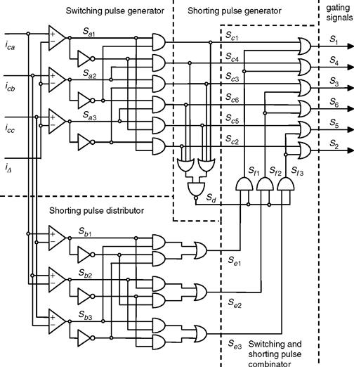
FIGURE 15.26 The three-phase CSI. Gating pattern generator for analog on-line carrier-based PWM.
It is composed of a switching pulse generator, a shorting pulse generator, a shorting pulse distributor, and a switching and shorting pulse combinator. The circuit basically produces the gating signals (s = [s1 …s6]T) according to a carrier iΔ and three modulating signals icabc = [ica icb ica]T. Therefore, any set of modulating signals which when combined result in a sinusoidal line-to-line set of signals, will satisfy the requirement for a sinusoidal line current pattern. Examples of such a modulating signals are the standard sinusoidal, sinusoidal with third harmonic injection, trapezoidal, and deadband waveforms.
The first component of this stage (Fig. 15.26) is the switching pulse generator, where the signals sa123 are generated according to:
![]() (15.50)
(15.50)
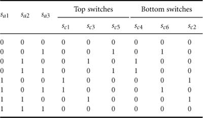
The outputs of the switching pulse generator are the signals sc, which are basically the gating signals of the CSI without the shorting pulses. These are necessary to freewheel the dc link current í when zero ac output currents are required. Table 15.5 shows the truth table of sc for all combinations of their inputs Sa123. It can be clearly seen that at most one top switch and one bottom switch is on, which satisfies the first constraint of the gating signals as stated before.
TABLE 15.5 Truth table for the switching pulse generator stage (Fig. 15.26)
In order to satisfy the second constraint, the shorting pulse (sd = 1) (sd = 1) is generated (shorting pulse generator (Fig. 15.26)) the top switches (sc1 = sC3 = sc5 = 0) or none of the bottom switches (sC4 = sc6 = sC2 = 0) are gated. Then, this pulse is added (using OR gates) to only one leg of the CSI (either to the switches 1 and 4, 3 and 6, or 5 and 2) by means of the switching and shorting pulse combinator (Fig. 15.26). The signals generated by the shorting pulse generator se123 ensure that: (a) only one leg of the CSI is shorted, as only one of the signals is HIGH at any time; and (b) there is an even distribution of the shorting pulse, as se23 is high for 120° in each period. This ensures that the rms currents are equal in all legs.
Figure 15.27 shows the relevant waveforms if a triangular carrier iΔ and sinusoidal modulating signals ic abc are used in combination with the gating pattern generator circuit (Fig. 15.26); this is SPWM in CSIs. It can be observed that some of the waveforms (Fig. 15.27) are identical to those obtained in three-phase VSIs, where a SPWM technique is used (Fig. 15.15). Specifically: (i) the load line voltage (Fig. 15.15d) in the VSI is identical to the load line current (Fig. 15.27d) in the CSI; and (ii) the dc link current (Fig. 15.15g) in the VSI is identical to the dc link voltage (Fig. 15.27g) in the CSI.
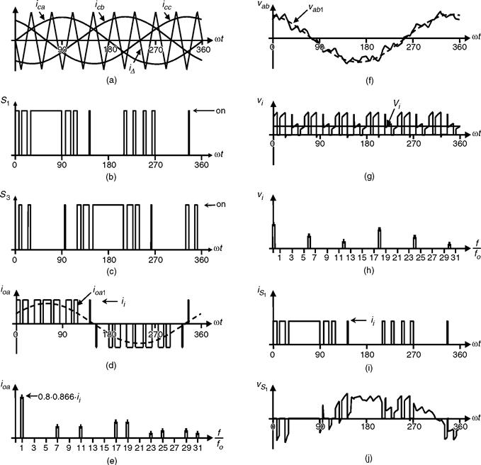
FIGURE 15.27 The three-phase CSI. Ideal waveforms for the SPWM (ma = 0.8, mf = 9): (a) carrier and modulating signals; (b) switch Si state; (c) switch S3 state; (d) ac output current; (e) ac output current spectrum; (f) ac output voltage; (g) de voltage; (h) de voltage spectrum; (i) switch Si current; and (j) switch Si voltage.
This brings up the duality issue between both the topologies when similar modulation approaches are used. Therefore, for odd multiples of 3 values of the normalized carrier frequency mf, the harmonics in the ac output current appear at normalized frequencies fh centered around mf and its multiples, specifically, at
![]() (15.51)
(15.51)
where l = 1,3,5,… for k = 2,4,6,… and l = 2,4,… for k = 1, 5,7,… such that h is not a multiple of 3. Therefore, the harmonics will be at mf ± 2, mf ± 4,…, 2mf ± 1,2mf ± 5,…, 3 mf ± 2, 3 mf ± 4,…, 4mf ± 1, 4mf ± 5, … For nearly sinusoidal ac load voltages, the harmonics in the dc link voltage are at frequencies given by
![]() (15.52)
(15.52)
where l = 0,2,4,… for k = 1,5,7,… and l = 1,3,5,… for k = 2,4,6,… such that h = l (mf ± k is positive and not a multiple of 3. For instance, Fig. 15.27h shows the sixth harmonic (h = 6), which is due to h = 1 9 − 2 − 1 = 6. Identical conclusions can be drawn for the small and large values of mf in the same way as for three-phase VSI configurations. Thus, the maximum amplitude of the fundamental ac output line current is ![]() and therefore one can write
and therefore one can write
![]() (15.53)
(15.53)
To further increase the amplitude of the load current, the overmodulation approach can be used. In this region, the fundamental line currents range in
![]() (15.54)
(15.54)
To further test the gating signal generator circuit (Fig. 15.26), a sinusoidal set with third and ninth harmonic injection modulating signals are used. Figure 15.28 shows the relevant waveforms.

FIGURE 15.28 Gating pattern generator. Waveforms for third and ninth harmonic injection PWM (ma = 0.8, mf = 15): signals as described in Fig. 15.26.
15.4.2 Square-wave Operation of Three-phase CSIs
As in VSIs, large values of ma in the SPWM technique lead to full overmodulation. This is known as square-wave operation. Figure 15.29 depicts this operating mode in a three-phase CSI, where the power valves are on for 120°. As presumed, the CSI cannot control the load current except by means of the dc link current l This is due to the fact that the fundamental ac line current expression is
![]() (15.55)
(15.55)
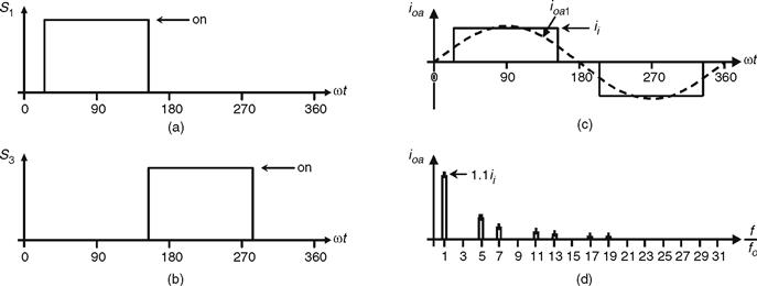
FIGURE 15.29 The three-phase CSI. Square-wave operation: (a) switch Si state; (b) switch S3 state; (c) ac output current; and (d) ac output current spectrum.
The ac line current contains the harmonics fh, where h = 6 k ± 1 (k = 1,2,3,…), and they feature amplitudes that is inversely proportional to their harmonic order (Fig. 15.29d). Thus,
![]() (15.56)
(15.56)
The duality issue among both the three-phase VSI and CSI should be noted especially in terms of the line-load waveforms. The line-load voltage produced by a VSI is identical to the load line current produced by the CSI when both are modulated using identical techniques. The next section will show that this also holds for SHE-based techniques.
15.4.3 Selective Harmonic Elimination in Three-phase CSIs
The SHE-based modulating techniques in VSIs define the gating signals such that a given number of harmonics are eliminated and the fundamental phase-voltage amplitude is controlled. If the required line output voltages are balanced and 120° out-of-phase, the chopping angles are used to eliminate only the harmonics at frequencies h = 5,7,11,13,… as required.
The circuit shown in Fig. 15.30 uses the gating signals sa123 developed for a VSI and a set of synchronizing signals icabc to obtain the gating signals s for a CSI. The synchronizing signals icabcaresinusoidal balanced waveforms that are synchronized with the signals sa123 in order to symmetrically distribute the shorting pulse and thus generate symmetrical gating patterns. The circuit ensures line current waveforms as the line voltages in a VSI. Therefore, any arbitrary number of harmonics can be eliminated and the fundamental line current can be controlled in CSIs. Moreover, the same chopping angles obtained for VSIs can be used in CSIs.
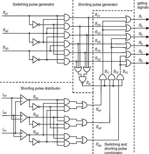
FIGURE 15.30 The three-phase CSI. Gating pattern generator for SHE PWM techniques.
For instance, to eliminate the fifth and seventh harmonics, the chopping angles are shown in Fig. 15.31, which are identical to that obtained for a VSI using Eq. (15.9). Figure 15.32 shows that the line current does not contain the fifth and the seventh harmonics as expected. Hence, any number of harmonics can be eliminated in three-phase CSIs by means of the circuit (Fig. 15.30) without the hassle of how to satisfy the gating signal constrains.
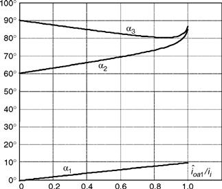
FIGURE 15.31 Chopping angles for SHE and fundamental current control in three-phase CSIs: fifth and seventh harmonic elimination.
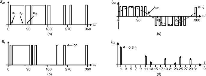
FIGURE 15.32 The three-phase CSI. Ideal waveforms for the SHE technique: (a) VSI gating pattern for fifth and seventh harmonic elimination; (b) CSI gating pattern for fifth and seventh harmonic elimination; (c) line current ioa for fifth and seventh harmonic elimination; and (d) spectrum of (c).
15.4.4 Space-vector-based Modulating Techniques in CSIs
The objective of the SV-based modulating technique is to generate PWM load line currents that are on average equal to given load line currents. This is done digitally in each sampling period by properly selecting the switch states from the valid ones of the CSI (Table 15.4) and the proper calculation of the period of times they are used. As in VSIs, the selection and time calculations are based upon the space-vector transformation.
A. Space-vector Transformation in CSIs
Similarly to VSIs, the vector of three-phase line-modulating signals icabc = [ica icb icc]T can be represented by the complex vector ![]() by means of Eqs. (15.36) and (15.37). For three-phase balanced sinusoidal modulating waveforms, which feature an amplitude
by means of Eqs. (15.36) and (15.37). For three-phase balanced sinusoidal modulating waveforms, which feature an amplitude ![]() and an angular frequency ω, the resulting modulating signals complex vector
and an angular frequency ω, the resulting modulating signals complex vector ![]() becomes a vector of fixed module
becomes a vector of fixed module ![]() , which rotates at frequency ω (Fig. 15.33). Similarly, the SV transformation is applied to the line currents of the nine states of the CSI normalized with respect to ii, which generates nine space vectors (
, which rotates at frequency ω (Fig. 15.33). Similarly, the SV transformation is applied to the line currents of the nine states of the CSI normalized with respect to ii, which generates nine space vectors (![]() , i = 1,2,…, 9 in Fig. 15.33). As expected,
, i = 1,2,…, 9 in Fig. 15.33). As expected, ![]() to
to ![]() are non-null line current vectors and
are non-null line current vectors and ![]() ,
, ![]() , and
, and ![]() are null line current vectors.
are null line current vectors.
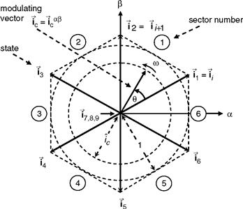
FIGURE 15.33 The space-vector representation in CSIs.
The SV technique approximates the line-modulating signal space vector ![]() by using the nine space vectors (
by using the nine space vectors (![]() , i = 1,2,…, 9) available in CSIs. If the modulating signal vector ic is between the arbitrary vectors
, i = 1,2,…, 9) available in CSIs. If the modulating signal vector ic is between the arbitrary vectors ![]() , and
, and ![]()
![]() , then
, then ![]() , and
, and ![]()
![]() combined with one zero SV (
combined with one zero SV (![]() =
= ![]() or
or ![]() or
or ![]() should be used to generate
should be used to generate ![]() . To ensure that the generated current in one sampling period Ts (made up of the currents provided by the vectors
. To ensure that the generated current in one sampling period Ts (made up of the currents provided by the vectors ![]() ,
, ![]() , and
, and ![]() used during times T, Ti,+ 1, and Tz) is on average equal to the vector
used during times T, Ti,+ 1, and Tz) is on average equal to the vector ![]() , the following expressions should hold:
, the following expressions should hold:
![]() (15.57)
(15.57)
![]() (15.58)
(15.58)
![]() (15.59)
(15.59)
where 0 ≤ ![]() ≤ 1. Although, the SVM technique selects the vectors to be used and their respective on-times, the sequence in which they are used, the selection of the zero space vector, and the normalized sampled frequency remain undetermined.
≤ 1. Although, the SVM technique selects the vectors to be used and their respective on-times, the sequence in which they are used, the selection of the zero space vector, and the normalized sampled frequency remain undetermined.
B. Space-vector Sequences and Zero Space-vector Selection
Although there is no systematic approach to generate a SV sequence, a graphical representation shows that the sequence ![]() ,
, ![]() (where the chosen
(where the chosen ![]() depends upon the sector) provides high performance in terms of minimizing unwanted harmonics and reducing the switching frequency. To obtain the zero SV that minimizes the switching frequency, it is assumed that Ic is in Sector $$. Then Fig. 15.34 shows all the possible transitions that could be found in Sector $$. It can be seen that the zero vector
depends upon the sector) provides high performance in terms of minimizing unwanted harmonics and reducing the switching frequency. To obtain the zero SV that minimizes the switching frequency, it is assumed that Ic is in Sector $$. Then Fig. 15.34 shows all the possible transitions that could be found in Sector $$. It can be seen that the zero vector ![]() should be chosen to minimize the switching frequency. Table 15.6 gives a summary of the zero space vector to be used in each sector in order to minimize the switching frequency. However, should be noted that Table 15.6 is valid only for the sequence
should be chosen to minimize the switching frequency. Table 15.6 gives a summary of the zero space vector to be used in each sector in order to minimize the switching frequency. However, should be noted that Table 15.6 is valid only for the sequence ![]() ,
, ![]() ,
, ![]() . Another sequence will require reformulating the zero space-vector selection algorithm.
. Another sequence will require reformulating the zero space-vector selection algorithm.
FIGURE 15.34 Possible state transitions in Sector $$ involving a zero SV: (a) transition: ![]() or
or ![]() (b) transition:
(b) transition: ![]() ; and (c) transition:
; and (c) transition: ![]() .
.
TABLE 15.6 Zero SV for minimum switching frequency in CSI and sequence ![]() ,
, ![]() ,
, ![]()
 |
C. The Normalized Sampling Frequency
As in VSIs modulated by a SV approach, the normalized sampling frequency fsn should be an integer multiple of 6 to minimize uncharacteristic harmonics. As an example, Fig. 15.35 shows the relevant waveforms of a CSI SVM for fsn = 18 and ![]() = 0.8. Figure 15.35 also shows that the first set of relevant harmonics load line current are at fsn.
= 0.8. Figure 15.35 also shows that the first set of relevant harmonics load line current are at fsn.
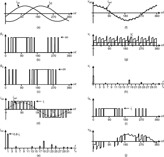
FIGURE 15.35 The three-phase CSI. Ideal waveforms for space-vector modulation ![]() : (a) modulating signals; (b) switch Si state; (c) switch S3 state; (d) ac output current; (e) ac output current spectrum; (f) ac output voltage; (g) de voltage; (h) de voltage spectrum; (i) switch S1 current; and (j) switch S1 voltage.
: (a) modulating signals; (b) switch Si state; (c) switch S3 state; (d) ac output current; (e) ac output current spectrum; (f) ac output voltage; (g) de voltage; (h) de voltage spectrum; (i) switch S1 current; and (j) switch S1 voltage.
15.4.5 DC Link Voltage in Three-phase CSIs
An instantaneous power balance indicates that
![]() (15.60)
(15.60)
where van(t), vbn(t), and vcn(t) are the phase filter voltages as shown in Fig. 15.36. If the filter is large enough and a relatively high switching frequency is used, the phase voltages become nearly sinusoidal balanced waveforms. On the other hand, if the ac output currents are considered sinusoidal and the dc link current is assumed constant ii(t) = Ii, Eq. (15.60) can be simplified to
 (15.61)
where Von is the rms ac output phase voltage, I01 is the rms fundamental line current, and ϕ is an arbitrary filter-load angle. Hence, the dc link voltage expression can be further simplified to the following:
![]() (15.62)
(15.62)
where V0 = ![]() is the rms load line voltage. The resulting dc link voltage expression indicates that the first line-current harmonic I01 generates a clean dc current. However, as the load line currents contain harmonics around the normalized sampling frequency fsn, the dc link current will contain harmonics but around fsn as shown in Fig. 15.35h. Similarly, in carrier-based PWM techniques, the dc link current will contain harmonics around the carrier frequency mf (Fig. 15.27).
is the rms load line voltage. The resulting dc link voltage expression indicates that the first line-current harmonic I01 generates a clean dc current. However, as the load line currents contain harmonics around the normalized sampling frequency fsn, the dc link current will contain harmonics but around fsn as shown in Fig. 15.35h. Similarly, in carrier-based PWM techniques, the dc link current will contain harmonics around the carrier frequency mf (Fig. 15.27).
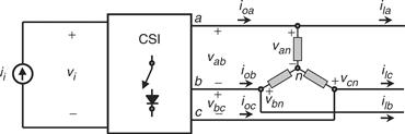
FIGURE 15.36 Phase-voltage definition in a wye-connected filter.
In practical implementations, a CSI requires a dc current source that should behave as a constant (as required by PWM CSIs) or variable (as square-wave CSIs) current source. Such current sources should be implemented as separate units and they are described earlier in this book.
15.5 Closed-loop Operation of Inverters
Inverters generate variable ac waveforms from a dc power supply to feed, for instance, ASDs. As the load conditions usually change, the ac waveforms should be adjusted to these new conditions. Also, as the dc power supplies are not ideal and the dc quantities are not fixed, the inverter should compensate for such variations. Such adjustments can be done automatically by means of a closed-loop approach. Inverters also provide an alternative to changing the load operating conditions (i.e. speed in an ASD).
There are two alternatives for closed-loop operation the feedback and the feedforward approaches. It is known that the feedback approach can compensate for both the perturbations (dc power variations) and the load variations (load torque changes). However, the feedforward strategy is more effective in mitigating perturbations as it prevents its negative effects at the load side. These cause-effect issues are analyzed in three-phase inverters in the following, although similar results are obtained for single-phase VSIs.
15.5.1 Feedforward Techniques in Voltage Source Inverters
The dc link bus voltage in VSIs is usually considered a constant voltage source vi. Unfortunately, and due to the fact that most practical applications generate the dc bus voltage by means of a diode rectifier (Fig. 15.37), the dc bus voltage contains low-order harmonics such as the sixth, twelfth,… (due to six-pulse diode rectifiers), and the second if the ac voltage supply features an unbalance, which is usually the case. Additionally, if the three-phase load is unbalanced, as in UPS applications, the dc input current in the inverter ii also contains the second harmonic, which in turn contributes to the generation of a second voltage harmonic in the dc bus.
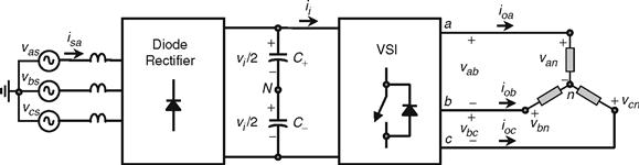
FIGURE 15.37 Three-phase VSI topology with a diode-based front-end rectifier.
The basic principle of feedforward approaches is to sense the perturbation and then modify the input in order to compensate for its effect. In this case, the dc link voltage should be sensed and the modulating technique should accordingly be modified. The fundamental ah line voltage in a VSI SPWM can be written as
![]() (15.63)
(15.63)
where ![]() is the carrier signal peak,
is the carrier signal peak, ![]() and
and ![]() are the modulating signal peaks, and vca(t) and vca(t) are the modulating signals. If the dc bus voltage v, varies around a nominal Vi value, then the fundamental line voltage varies proportionally; however, if the carrier signal peak
are the modulating signal peaks, and vca(t) and vca(t) are the modulating signals. If the dc bus voltage v, varies around a nominal Vi value, then the fundamental line voltage varies proportionally; however, if the carrier signal peak ![]() is redefined as
is redefined as
![]() (15.64)
(15.64)
where ![]() is the carrier signal peak (Fig. 15.38), then the resulting fundamental ab line voltage in a VSI SPWM is
is the carrier signal peak (Fig. 15.38), then the resulting fundamental ab line voltage in a VSI SPWM is
![]() (15.65)
(15.65)
where, clearly, the result does not depend upon the variations of the dc bus voltage.
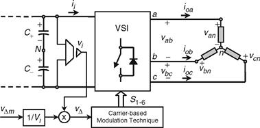
FIGURE 15.38 The three-phase VSI. Feedforward control technique to reject dc bus voltage variations.
Figure 15.39 shows the waveforms generated by the SPWM under a severe dc bus voltage variation (a second harmonic has been added manually to a constant Vi). As a consequence, the ac line voltage generated by the VSI is distorted as it contains low-order harmonics (Fig. 15.39e). These operating conditions may not be acceptable in standard applications such as ASDs because the load will draw distorted three-phase currents as well. The feedforward loop performance is illustrated in Fig. 15.40. As expected, the carrier signal is modified so as to compensate for the dc bus voltage variation (Fig. 15.40b). This is probed by the spectrum of the ac line voltage that does not contain low-order harmonics (Fig. 15.40e). It should be noted that ![]() >
> ![]() ,
, ![]() ; therefore, the compensation capabilities are limited by the required ac line voltage.
; therefore, the compensation capabilities are limited by the required ac line voltage.
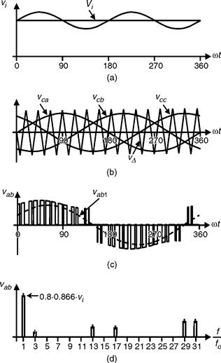
FIGURE 15.39 The three-phase VSI. Waveforms for regular SPWM (ma = 0.8, mf = 9): (a) dc bus voltage; (b) carrier and modulating signals; (c) ac output voltage; and (d) ac output voltage spectrum.
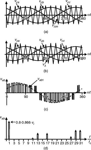
FIGURE 15.40 The three-phase VSI. Waveforms for SPWM including a feedforward loop (ma = 0.8, mf = 9): (a) carrier and modulating signals; (b) modified carrier and modulating signals; (c) ac output voltage; and (d) ac output voltage spectrum.
The performance of the feedforward approach depends upon the frequency of the harmonics present in the dc bus voltage and the carrier signal frequency. Fortunately, the relevant unwanted harmonics to be found in the dc bus voltage are the second, due to unbalanced supply voltages, and/or the sixth as the dc bus voltage is generated by means of a six-pulse diode rectifier. Therefore, a carrier signal featuring a 15-pu frequency is found to be sufficient to properly compensate for dc bus voltage variations.
Unbalanced loads generate a dc input current ii that contains a second harmonic, which contributes to the dc bus voltage variation. The previous feedforward approach can compensate for such perturbation and maintain balanced ac load voltages.
Digital techniques can also be modified in order to compensate for dc bus voltage variations by means of a feedforward approach. For instance, the SVM techniques indicate that the on-times of the vectors ![]() ,
, ![]() , and
, and ![]() are
are
![]() (15.66)
(15.66)
![]() (15.67)
(15.67)
![]() (15.68)
(15.68)
respectively, where ![]() is the amplitude of the desired ac line voltage, as shown in Fig. 15.18. By redefining this quantity to
is the amplitude of the desired ac line voltage, as shown in Fig. 15.18. By redefining this quantity to
![]() (15.69)
(15.69)
where Vi is the nominal dc bus voltage and vi(t) is the actual dc bus voltage. Thus, the on-times become
![]() (15.70)
(15.70)
![]() (15.71)
(15.71)
![]() (15.72)
(15.72)
where ![]() is the desired maximum ac line voltage. The previous expressions account for dc bus voltage variations and behave as a feedforward loop as it needs to sense the perturbation in order to be implemented. The previous expressions are valid for the linear region, thus
is the desired maximum ac line voltage. The previous expressions account for dc bus voltage variations and behave as a feedforward loop as it needs to sense the perturbation in order to be implemented. The previous expressions are valid for the linear region, thus ![]() is restricted to 0 <
is restricted to 0 < ![]() 1, which indicates that the compensation is indeed limited.
1, which indicates that the compensation is indeed limited.
15.5.2 Feedforward Techniques in Current Source Inverters
The duality principle between the voltage and the current source inverters indicates that, as described previously, the feedforward approach can be used for CSIs as well as for VSIs. Therefore, low-order harmonics present in the dc bus current can be compensated for before they appear at the load side. This can be done for both analog-based (e.g. carrier-based) and digital-based (e.g. space-vector) modulating techniques.
15.5.3 Feedback Techniques in Voltage Source Inverters
Unlike the feedforward approach, the feedback techniques correct the input to the system (gating signals) depending upon the deviation of the output to the system (e.g. ac load line currents in VSIs). Another important difference is that feedback techniques need to sense the controlled variables. In general, the controlled variables (output to the system) are chosen according to the control objectives. For instance, in ASDs, it is usually necessary to keep the motor line currents equal to a given set of sinusoidal references. Therefore, the controlled variables become the ac line currents. There are several alternatives to implement feedback techniques in VSIs, and three of them are discussed in the following.
A. Hysteresis Current Control
The main purpose here is to force the ac line current to follow a given reference. The status of the power valves S1 and S4 are changed whenever the actual ioa current goes beyond a given reference ioa,ref ± Δi/2. Figure 15.41 shows the hysteresis current controller for phase a. Identical controllers are used in phase b and c. The implementation of this controller is simple as it requires an operational amplifier (op-amp) operating in the hysteresis mode, thus the controller and modulator are combined in one unit.
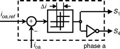
FIGURE 15.41 The three-phase VSI. Hysteresis current control (phase a).
Unfortunately, there are several drawbacks associated with the technique itself. First, the switching frequency cannot be predicted as in carrier-based modulators and therefore the harmonic content of the ac line voltages and currents becomes random (Fig. 15.42d). This could be a disadvantage when designing the filtering components. Second, as three-phase loads do not have the neutral connected as in ASDs, the load currents add up to zero. This means that only two ac line currents can be controlled independently at any given instant. Therefore, one of the hysteresis controllers is redundant at a given time. This explains why the load current goes beyond the limits and introduces limit cycles (Fig. 15.42a). Finally, although the ac load currents add up to zero, the controllers cannot ensure that all load line currents feature a zero dc component in one load cycle.
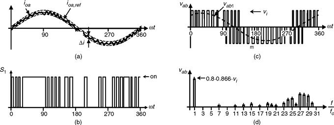
FIGURE 15.42 The three-phase VSI. Ideal waveforms for hysteresis current control: (a) actual ac load current and reference; (b) switch S1 state; (c) ac output voltage; and (d) ac output voltage spectrum.
B. Linear Control of VSIs
Proportional and proportional-integrative controllers can also be used in VSIs. The main purpose is to generate the modulating signals vca, vcb, and vcc in a closed-loop fashion as depicted in Fig. 15.43. The modulating signals can be used by a carrier-based technique such as the SPWM (as depicted in Fig. 15.43) or by space vector modulation. Because the load line currents add up to zero, the load line current references must add up to zero. Thus, the abc/αβγ transformation can be used to reduce to two controllers the overall implementation scheme as the γ component is always zero. This avoids limit cycles in the ac load currents.
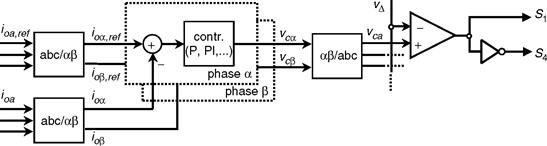
FIGURE 15.43 The three-phase VSI. Feedback control based on linear controllers.
The transformation of a set of variables in the stationary abc frame Xabc into a set of variables in the stationary αβ frame Xαβ is given by
![]() (15.73)
(15.73)
The selection of the controller (P, PI,…) is done according to the control procedures such as steady-state error, settling time, overshoot, and so forth. Figure 15.44 shows the relevant waveforms of a VSI SPWM controlled by means of a PI controller as shown in Fig. 15.43.
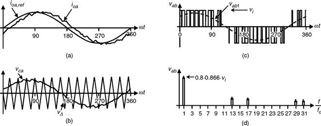
FIGURE 15.44 The three-phase VSI. Ideal waveforms for a PI controller in a feedback loop (ma, = 0.8, mf = 15): (a) actual ac load current and reference; (b) carrier and modulating signals; (c) ac output voltage; and (d) ac output voltage spectrum.
Although it is difficult to prove that no limit cycles are generated, the ac line current appears very much sinusoidal. Moreover, the ac line voltage generated by the VSI preserves the characteristics of such waveforms generated by SPWM modulators. This is confirmed by the harmonic spectrum shown in Fig. 15.44d, where the first set of characteristic harmonics are around the normalized carrier frequency mf = 15.
However, an error between the actual ioa and the ac line current reference ioa, ref can be observed (Fig. 15.44a). This error is inherent to linear controllers and cannot be totally eliminated, but it can be minimized by increasing the gain of the controller. However, the noise in the circuit is also increased, which could deteriorate the overall performance of the control scheme. The inherent presence of the error in this type of controllers is due to the fact that the controller needs a sinusoidal error to generate sinusoidal modulating signals vca, vcb, and vcc, as required by the modulator. Therefore, an error must exist between the actual and the ac line current references.
Nevertheless, as current-controlled VSIs are actually the inner loops in many control strategies, their inherent errors are compensated by the outer loop. This is the case of ASDs, where the outer speed loop compensates the inner current loops. In general, if the outer loop is implemented with dc quantities (such as speed), it can compensate the ac inner loops (such as ac line currents). If it is mandatory that a zero steady-state error be achieved with the ac quantities, then a stationary (abc frame) to rotating (dq frame) transformation is a valid alternative to use.
C. Linear Control of VSIs in a Rotating Frame
The rotating dq transformation allows ac three-phase circuits to be operated as if they were dc circuits. This is based upon a mathematical operation, that is the transformation of a set of variables in the stationary abc frame xabc into a set of variables in the rotating dq0 frame xdq0. The transformation is given by
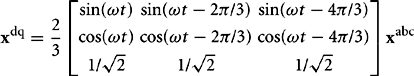 (15.74)
where ω is the angular frequency of the ac quantities. For instance, the current vector given by
 (15.75)
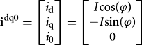 (15.76)
where I and ϕ are the amplitude and phase of the line currents, respectively. It can be observed that: (a) the zero component o is always zero as the three-phase quantities add up to zero; and (b) the d and q components id, iq are dc quantities. Thus, linear controllers should help to achieve zero steady-state error. The control strategy shown in Fig. 15.45 is an alternative where the zero-component controller has been eliminated due to fact that the line currents at the load side add up to zero.
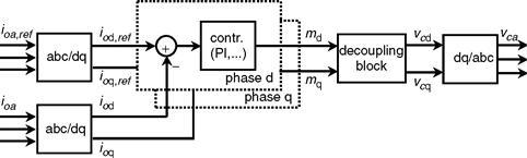
FIGURE 15.45 The three-phase VSI. Feedback control based on dqo transformation.
The controllers in Fig. 15.45 include an integrator that generates the appropriate dc outputs md and mq even if the actual and the line current references are identical. This ensures that the zero steady-state error is achieved. The decoupling block in Fig. 15.45 is used to eliminate the cross-coupling effect generated by the dq0 transformation and to allow an easier design of the parameters of the controllers.
The dq0 transformation requires the intensive use of multiplications and trigonometric functions. These operations can readily be done by means of digital microprocessors. Also, analog implementations would indeed be involved.
15.5.4 Feedback Techniques in Current Source Inverters
Duality indicates that CSIs should be controlled as equally as VSIs except that the voltages become currents and the currents become voltages. Thus, hystersis, linear and dq linear-based control strategies are also applicable to CSIs; however, the controlled variables are the load voltages instead of the load line currents.
For instance, the linear control of a CSI based on a dq transformation is depicted in Fig. 15.46. In this case, a passive balanced load is considered. In order to show that zero steady-state error is achieved, the per phase equations of the converter are written as
![]() (15.77)
(15.77)
![]() (15.78)
(15.78)
the ac line currents are in fact imposed by the modulator and they satisfy
![]() (15.79)
(15.79)
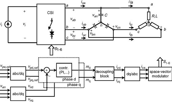
FIGURE 15.46 The three-phase CSI. Feedback control based on dq0 transformation.
Replacing Eq. (15.79) into the model of the converter Eqs. (15.77) and (15.78), using the dq0 transformation and assuming null zero component, the model of the converter becomes
![]() (15.80)
(15.80)
![]() (15.81)
(15.81)
where W is given by
![]() (15.82)
(15.82)
A first approximation is to assume that the decoupling block is not there; in other words, icdq = mdq. On the other hand, the model of the controllers can be written as
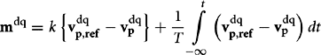 (15.83)
where k and T are the proportional and integrative gains of the PI controller that are chosen to achieve a desired dynamic response. Combining the model of the controllers and the model of the converter in dq coordinates and using the Laplace transform, the following relationship between the reference and actual load-phase voltages is found:
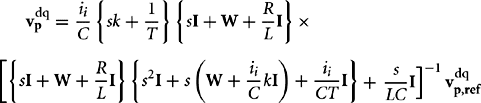 (15.84)
Finally, in order to prove that the zero steady-state error is achieved for step inputs in either the d or q component of the load-phase voltage reference, the previous expression is evaluated in 5 = 0. This results in the following:
![]() (15.85)
(15.85)
As expected, the actual and reference values are identical. Finally, the relationship in Eq. (15.84) is a matrix that is not diagonal. This means that both the actual and the reference load-phase voltages are coupled. In order to obtain a decoupled control, the decoupling block in Fig. 15.46 should be properly chosen.
15.6 Regeneration in Inverters
Industrial applications are usually characterized by a power flow that goes from the ac distribution system to the load. This is, for example, the case of an ASD operating in the motoring mode. In this instance, the active power flows from the dc side to the ac side of the inverter. However, there are an important number of applications in which the load may supply power to the system. Moreover, this could be an occasional condition as well as a normal operating condition. This is known as the regenerative operating mode. For example, when an ASD reduces the speed of an electrical machine this can be considered a transient condition. Downhill belt conveyors in mining applications can be considered as a normal operating condition. In order to simplify the notation, it could be said that an inverter operates in the motoring mode when the power flows from the dc to the ac side, and in the regenerative mode when the power flows from the ac to the dc side.
15.6.1 Motoring Operating Mode in Three-phase VSIs
This is the case where the power flows from the dc side to the ac side of the inverter. Figure 15.47 shows a simplified scheme of an ASD where the motor has been modeled by three RLe branches, where the sources eabc are the back-emf. Because the ac line voltages applied by the inverter are imposed by the pulsewidth modulation technique being used, they can be adjusted according to specific requirements. In particular, Fig. 15.48 shows the relevant waveforms in steady state for the motoring operating mode of the ASD. To simplify the analysis, a constant dc bus voltage vi = Vi has been considered.
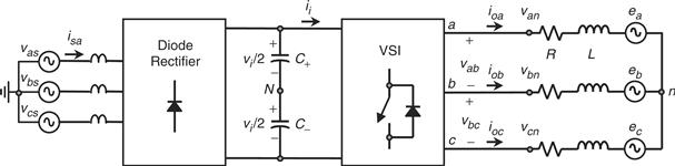
FIGURE 15.47 Three-phase VSI topology with a diode-based front-end rectifier.
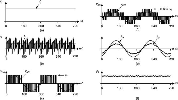
FIGURE 15.48 The ASD based on a VSI. Motoring mode: (a) dc bus voltage; (b) dc bus current; (c) ac line-load voltage; (d) ac phase-load voltage; (e) motor line current and back-emf; and (f) shaft power.
It can be observed that: (i) the dc bus current ii features a dc value Ii that is positive; and (ii) the motor line current is in phase with the back-emf. Both features confirm that the active power flows from the dc source to the motor. This is also confirmed by the shaft power plot (Fig. 15.48f), which is obtained as:
![]() (15.86)
(15.86)
15.6.2 Regenerative Operating Mode in Three-phase VSIs
The back-emf sources eabc are functions of the machine speed and as such they ideally change just as the speed changes.
The regeneration operating mode can be achieved by properly modifying the ac line voltages applied to the machine. This is done by the speed outer loop that could be based on a scalar (e.g. V/f) or vectorial (e.g. field-oriented) control strategy. As indicated earlier, there are two cases of regenerative operating modes.
A. Occasional Regenerative Operating Mode
This mode is required during transient conditions such as in occasional braking of electrical machines (ASDs). Specifically, the speed needs to be reduced and the kinetic energy is taken into the dc bus. Because the motor line voltage is imposed by the VSI, the speed reduction should be done in such a way that the motor line currents do not exceed the maximum values. This boundary condition will limit the ramp-down speed to a minimum, but shorter braking times will require a mechanical braking system.
Figure 15.49 shows a transition from the motoring to regenerative operating mode for an ASD as shown in Fig. 15.47. Here, a stiff dc bus voltage has been used. Zone I in Fig. 15.49 is the motoring mode, Zone II is a transition condition, and Zone III is the regeneration mode. The line voltage is adjusted dynamically to obtain nominal motor line currents during regeneration (Fig. 15.49d). Zone III clearly shows that the shaft power gets reversed.
FIGURE 15.49 The ASD based on a VSI. Motoring to regenerative operating mode transition: (a) dc bus current; (b) ac line motor voltage; (c) ac phase motor voltage; (d) motor line current and back-emf; and (e) shaft power.
Occasional regeneration means that the drive rarely goes into this operating mode. Therefore, such energy can be: (a) left uncontrolled or (b) burned in resistors that are paralleled to the dc bus. The first option is used in low- to medium-power applications that use diode-based front-end rectifiers. Therefore, the dc bus current flows into the dc bus capacitor and the dc bus voltage rises accordingly to
![]() (15.87)
(15.87)
where Δvi, is the dc bus voltage variation, C is the dc bus voltage capacitor, Ii is the average dc bus current during regeneration, and Δt is the duration of the regeneration operating mode. Usually, the drives have the capacitor C designed to allow a 10% overvoltage in the dc bus.
The second option uses burning resistors RR that are paralleled in the dc bus as shown in Fig. 15.50 by means of the switch SR. A closed-loop strategy based on the actual dc bus voltage modifies the duty cycle of the turn-on/turn-off of the switch SR in order to keep such voltage under a given reference. This alternative is used when the energy recovered by the VSI would result in an acceptable dc bus voltage variation if an uncontrolled alternative is used.
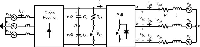
FIGURE 15.50 The ASD based on a VSI. Burning resistor strategy.
There are some special cases where the regeneration operating mode is frequently used. For instance, electrical shovels in mining companies have repetitive working cycles and ≈ 15% of the energy is sent back into the dc bus. In this case, a valid alternative is to send back the energy into the ac distribution system.
The schematic shown in Fig. 15.51 is capable of taking the kinetic energy and sending it into the ac grid. As reviewed earlier, the regeneration operating mode reverses the polarity of the dc current i, and because the diode-based front-end converter cannot take negative currents, a thyristor-based front-end converter is added. Similarly to the burning-resistor approach, a closed-loop strategy based on the actual dc bus voltage vi modifies the commutation angle α of the thyristor rectifier in order to keep such voltage under a given reference.
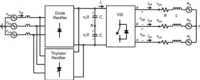
FIGURE 15.51 The ASD based on a VSI. Diode-thyristor-based front-end rectifier with regeneration capabilities.
B. Regenerative Operating Mode as Normal operating Mode
Fewer industrial applications are capable of returning energy into the ac distribution system on a continuous basis. For instance, mining companies usually transport their product downhill for a few kilometers before processing it. In such cases, the drive maintains the transportation belt conveyor at constant speed and takes the kinetic energy. Due to the large amount of energy and the continuous operating mode, the drive should be capable of taking the kinetic energy, transforming it into electrical energy, and sending it into the ac distribution system. This would make the drive a generator that would compensate for the active power required by other loads connected to the electrical grid.
The schematic shown in Fig. 15.52 is a modern alternative for adding regeneration capabilities to the VSI-based drive on a continuous basis. In contrast to the previous alternatives, this scheme uses a VSI topology as an active front-end converter, which is generally called voltage-source rectifier (VSR). The VSR operates in two quadrants, that is, positive dc voltages and positive/negative dc currents as reviewed earlier. This feature makes it a perfect match for ASDs based on a VSI. Some of the advantages of using a VSR topology are: (i) the ac supply current can be as sinusoidal as required (by increasing the switching frequency of the VSR or the ac line inductance); (ii) the operation can be done at a unity displacement power factor in both motoring and regenerative operating modes; and (iii) the control of the VSR is done in both motoring and regenerative operating modes by a single dc bus voltage loop.

FIGURE 15.52 The ASD based on a VSI. Active front-end rectifier with regeneration capabilities.
15.6.3 Regenerative Operating Mode in Three-phase CSIs
There are drives where the motor side converter is a CSI. This is usually the case where near sinusoidal motor voltages are needed instead of the PWM type of waveform generated by VSIs. This is normally the case for medium-voltage applications. Such inverters require a dc current source that is constructed by means of a controlled rectifier.
Figure 15.53 shows a CSI-based ASD where the dc current source is generated by means of a thyristor-based rectifier in combination with a dc link inductor Ldc. In order to maintain a constant dc link current ii = Ii, the thyristor-based rectifier adjusts the commutation angle α by means of a closed-loop control strategy. Assuming a constant dc link current, the regenerating operating mode is achieved when the dc link voltage vi reverses its polarity. This can be done by modifying the PWM pattern applied to the CSI as in the VSI-based drive. To maintain the dc link current constant, the thyristor-based rectifier also reverses its dc link voltage vr. Fortunately, the thyristor rectifier operates in two quadrant, that is, positive dc link currents and positive/negative dc link voltages.
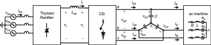
FIGURE 15.53 The ASD based on a CSI. Thyristor-based rectifier.
Thus, no additional equipment is required to include regeneration capabilities in CSI-based drives.
Similarly, an active front-end rectifier could be used to improve the overall performance of the thyristor-based rectifier. A PWM current-source rectifier (CSR) could replace the thyristor-based rectifier with the following added advantages: (i) the ac supply current can be as sinusoidal as required (e.g. by increasing the switching frequency of the CSR); (ii) the operation can be done at a unity displacement power factor in both motoring and regenerative operating modes; and (iii) the control of the CSR is done in both motoring and regenerative operating modes by a single dc bus current loop.
15.7 Multistage Inverters
The most popular three-phase voltage source inverter (VSI) consists of a six-switch topology (Fig. 15.54a). The topology can generate a three-phase set of ac line voltages such that each line voltage vab (Fig. 15.54b) features a fundamental ac line voltage vab1 and unwanted harmonics Fig. 15.54c. The fundamental ac line voltage is usually required as a sinusoidal waveform at variable amplitude and frequency, and the unwanted harmonics are located at high frequencies. These requirements are met by means of a modulating technique as shown earlier. Among the applications in low-voltage ranges of six-switch VSIs are the adjustable speed drives (ASDs). The range is in low voltages due to: (a) the high dv/dt present in the PWM ac line voltages (Fig. 15.54b), which will be unacceptable in the medium- to high-voltage ranges and (b) the load power would be shared only among six switches. This may require paralleling and series-connected power valves, an option usually avoided as symmetrical sharing of the power is not natural in these arrangements.
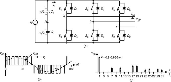
FIGURE 15.54 Six-switch voltage source inverter (mf = 9, ma = 0.8): (a) power topology; (b) ac output voltage; and (c) ac output voltage spectrum.
Two solutions are available to generate near-sinusoidal voltage waveforms while using six-switch topologies. The first is a topology based on a CSI in combination with a capacitive filter. The second solution is a topology based on a VSI including an inductive or inductive/capacitive filter at the load terminals. Although both alternatives generate near-sinusoidal voltage waveforms, both continue sharing the load power only among six power valves.
Solutions based on multistage voltage source topologies have been proposed. They provide medium voltages at the ac terminals while keeping low dv/dts and a large number of power valves that symmetrically share the total load power. The multistage VSIs can be classified in multicell and multilevel topologies.
15.7.1 Multicell Topologies
The goal is to develop a new structure with improved performance based on standard structures that are known as cells. For instance, Fig. 15.55a shows a cell featuring a three-phase input and a single-phase output. The front-end converter is a six-diode-based rectifier, and a single-phase VSI generates a single-phase ac voltage v0. Figure 15.55b and c shows characteristic waveforms where a sinusoidal unipolar PWM (mf = 6, ma = 0.8) has been used to modulate the inverter.
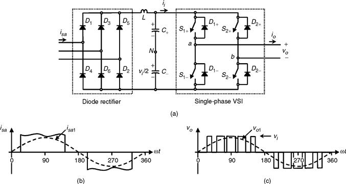
FIGURE 15.55 Three-phase-input single-phase output cell: (a) power topology; (b) ac input current, phase a; and (c) ac output voltage (mf = 6, ma = 0.8).
Standard cells are meant to be used at low voltages, thus they can use standard components that are less expensive and widely available. The new structure should generate near-sinusoidal ac load voltages, draw near-sinusoidal ac line currents, and more importantly the load voltages should feature moderate dv/dts.
Figure 15.56 shows a multicell converter that generates a three-phase output voltage out of a three-phase ac distribution system. The structure uses three standard cells (as shown in Fig. 15.55) connected in series to form one phase; thus the phase-load voltages are the sum of the single-phase voltages generated by each cell. For instance, the phase voltage a is given by
![]() (15.88)
(15.88)
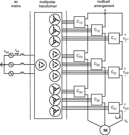
FIGURE 15.56 Multistage converter based on a multicell arrangement.
In order to maximize the load-phase voltages, the ac voltages generated by the cells should feature identical fundamental components. On the other hand, each cell generates a PWM voltage waveform at the ac side, which contains unwanted voltage harmonics. If a carrier-based modulating technique is used, the harmonics generated by each cell are at well-defined frequencies (Fig. 15.55c). Some of these harmonics are not present in the phase-load voltage if the carrier signals of each cell are properly phase shifted.
In fact, Fig. 15.57 shows the voltages generated by cells c11, C21, and C31, which are v011, v021, and v031, respectively, and form the load-phase voltage a. They are generated using the unipolar SPWM approach, that is, one modulating signal vca and three carrier signals VΔ 1, vΔ 2, and vΔ 3 that are used by cells c11, c21, and c31, respectively (Fig. 15.57a). The carrier signals have a normalized frequency mf, which ensures an mf switching frequency in each power valve and the lowest unwanted set of harmonics ≈ 2(mf (mf even) in the ac cell voltages v011, v021, and v031. More importantly, the carrier signals are ψ = 60° out-of-phase, which ensures the lowest unwanted set of voltage harmonics ≈ 6. mf in the load-phase voltage van, that is, the lowest set of harmonics in Fig. 15.57f is 6 mf = 6 6 = 36.
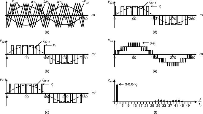
FIGURE 15.57 Multicell topology. Cell voltages in phase o using a unipolar SPWM (mf = 6, ma = 0.8): (a) modulating and carrier signals; (b) cell C11 ac output voltage; (c) cell C21 ac output voltage; (d) cell C31 ac output voltage; (e) phase o load voltage; and (f) phase o load-voltage spectrum.
This can be explained as follows. The voltage harmonics present in the PWM voltage of each cell are at l mf ± k, l = 2,4,… (where k = 1,3, 5,…); for instance, for mf = 6, the first set of harmonics is at 12 ± 1, 12 ± 3, … in all cells. Because the cells in one phase use carrier signals that are 60° out-of-phase, all the voltage harmonics ≈ 1 mf in all cells are l ( 60° out-of-phase. Therefore, for l = 2, the cell c11 generates the harmonics l mf ± k = 2 mf ± k at a given phase f, the cell C21 generates the harmonics 2 mf ± k at a phase f + l ( 60° = f + 2 (60° = f + 120° = f - 240°, and the cell C21 generates the harmonics 2 mf ± k at a phase f - l.60° = f - 2 60° = f - 120° = f + 240°; thus, if the voltages have identical amplitudes, the harmonics ≈ 2 (mf add up to zero. Similarly, for l = 4, the cell c11 generates the harmonics l (mf ± k = 4 mf ± k at a given phase f, the cell C21 generates the harmonics 4 (mf ± k at a phase f + l (60° = f + 4 60° = f + 240° = f - 120°, and the cell C21 generates the harmonics 4. mf ± k at a phase f + 1. 60° = f - 4 60° = f – 240° = f + 120°; thus, if the voltages have identical amplitudes, the harmonics ≈ 2.mf add up to zero. However, for l = 6, the cell en generates the harmonics l mf ± k = 6 (mf ± k at a given phase f, the cell C21 generates the harmonics 6 (mf ± k at a phase f + l (60° = f + 6 60° = f + 360° = f, and the cell c21 generates the harmonics 6 (mf ± k at a phase f − 1 60° = f − 6 60° = f − 360° = f; thus, if the voltages have identical amplitudes, the harmonics ≈ 6.mf become triplicated rather than cancelled out.
In general, due to the fact that nc = 3, cells are connected in series in each phase, nc carriers are required, which should be ψ = 180°/nc out-of-phase. The number of cells per phase nc depends on the required phase voltage. For instance, a 600 V dc cell generates an ac voltage of ≈ 600/(2 = 424V. Then three cells connected in series generate a phase voltage of 3 424 = 1.27 kV, which in turn generates a 1.27 (3 = 2.2 kV line-to-line voltage.
Phases b and c are generated similarly to phase a. However, the modulating signals vcb and vcc should be 120° out-of-phase. In order to use identical carrier signals in phases b and c, the carrier-normalized frequency mf should be a multiple of 3. Thus, three modulating signals and nc carrier signals are required to generate three phase voltages by means of a multicell approach, where nc depends upon the required load line voltage and the dc bus voltage of each cell.
The ac supply current of each cell is a six-pulse type of current as shown in Fig. 15.58, which feature harmonics at 6 k± 1 (k = 1,2,…). Similarly to the load side, the ac supply currents of each cell are combined so as to achieve high-performance overall supply currents. Because the front-end converter of each cell is a six-pulse diode rectifier, a multipulse approach is used. This is based on the natural harmonic cancellation when, for instance, a wye to delta/wye transformer is used to form an N = 12-pulse configuration from two six-pulse diode rectifiers. In this case, the fifth and seventh harmonics are cancelled out because the supply voltages applied to each six-pulse rectifier become 30° out-of-phase. In general, to form an N = 6 ns pulse configuration, ns set of supply voltages that should be 60°/ns out-of-phase is required. This would ensure the first set of unwanted current harmonics at 6 ns ± 1.
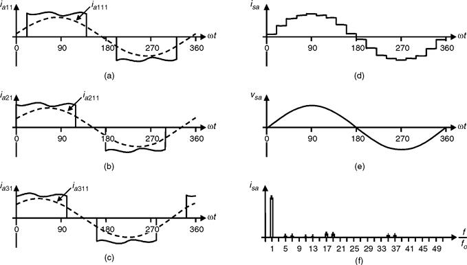
FIGURE 15.58 Multicell topology. Ac input current, phase o: (a) cell en; (b) cell C21; (c) cell C31; (d) overall supply current; (e) supply phase voltage; and (f) overall supply current spectrum.
The configuration depicted in Fig. 15.56 contains nc = 9 cells, and a transformer capable of providing ns = 9 sets of three-phase voltages that should be 60°/ns − 60°/9 out-of-phase to form an N = 6 ·ns = 6 · 9 = 54-pulse configuration is required. Although this alternative would provide a near-sinusoidal overall supply current, a fewer number of pulses are also acceptable that would reduce the transformer complexity. An N = 18-pulse configuration usually satisfies all the requirements. In the example, this configuration can be achieved by means of a transformer with nc = 9 isolated secondaries; however, only ns = 3 set of three-phase voltages that are 607ns = 6073 = 20° out-of-phase are generated (Fig. 15.56). The configuration of the transformer restricts the connection of the cells in groups of three as shown in Fig. 15.56. In this case, the fifth, seventh, eleventh, and thirteenth harmonics are cancelled out and thus the first set of harmonics in the supply currents are the seventeenth and the nineteenth. Figure 15.58d shows the resulting supply current that is near-sinusoidal and Fig. 15.58f shows the corresponding spectrum. The fifth, seventh, eleventh, and thirteenth harmonics are still there, which is due to the fact that the ac input currents in each cell are not exactly the six-pulse type of waveforms as seen in Fig. 15.58a, b, and c. This is mainly because: (i) the dc link in the cells contains a small inductor L, which does not smooth out sufficiently the debus current (Fig. 15.55a) and (ii) the transformer leakage inductance (or added line inductance) smoothes out the edges of the current, which also contributes to the reactive power required by the cells. This last effect is not shown in Fig. 15.58a, b, and c.
15.7.2 Voltage Source-based Multilevel Topologies
The six-switch VSI is usually called a two-level VSI due to the fact that the inverter phase voltages vaN, VbN, and vCN (Fig. 15.54a) are instantaneously either vi/2 or − vi/2. In other words, the phase voltages can take one of the two voltage levels. Multilevel topologies provide an alternative to these voltages to take one value out of N levels. For instance, Fig. 15.59 shows an N = 3-level topology, where the values of the inverter phase voltage are either vi/2, 0, or — vi,/2 (Fig. 15.60d). An interesting problem is how to obtain the gating pattern for the 12 switches required in an N = 3-level topology. There are several modulating techniques to overcome this problem, which can be classified as analog (e.g. carrier-based) and digital (SV-based). Both approaches have to deal with the valid switch states of the inverter.
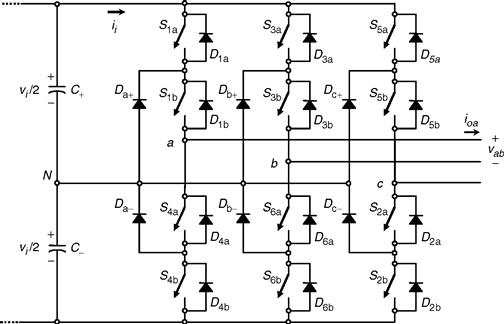
FIGURE 15.59 Three-phase three-level VSI topology.
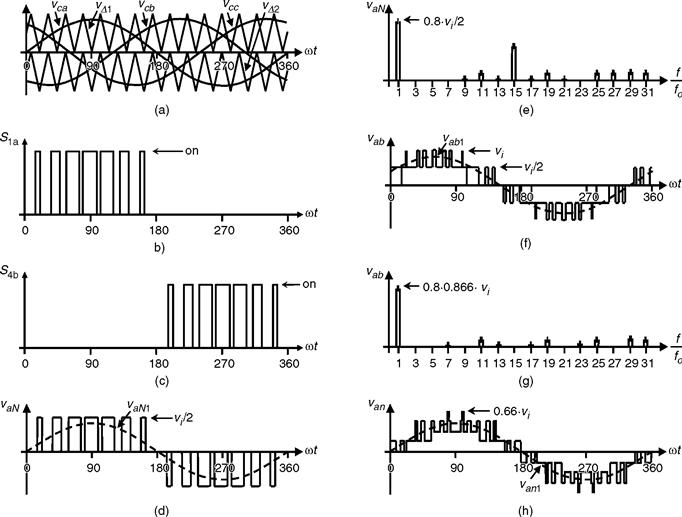
FIGURE 15.60 Three-level VSI topology. Relevant waveforms using a SPWM (mf = 15, ma = 0.8): (a) modulating and carrier signals; (b) switch S1a status; (c) switch S4b, status; (d) inverter phase o voltage; (e) inverter phase o voltage spectrum; (f) load line voltage; (g) load line voltage spectrum; and (h) load phase o voltage.
A. Valid Switch States in a Three-level VSI
The easiest way of obtaining the valid switch states is to analyze each phase separately. Phase a contains the switches S1a, S1b, S4a, and S4b,, which cannot be on simultaneously because a short circuit across the dc bus would be produced, and cannot be off simultaneously because an undefined phase voltage vaN would be produced. A summary of the valid switch combinations is given in Table 15.7. It is important to note that all valid switch combinations satisfy the condition that switch S1a state is always the opposite to switch S4a, state, and that switch S1b, state is always the opposite to switch S4b, state. Any other switch-state combination would result in an undefined inverter phase a voltage because it will depend upon the load-phase current ioa polarity. The switch states for phases b and c are identical to that of phase a; moreover, because they are paralleled, they can operate in an independent manner.
TABLE 15.7 Valid switch states for a three-level VSI, phase a
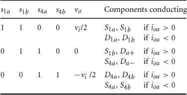
B. The SPWM Technique in Three-level VSIs
The main objective is to generate the appropriate 12 gating signals so as to obtain fundamental inverter phase voltages equal to a given set of modulating signals. Specifically, the SPWM in three-level inverters uses a sinusoidal set of modulating signals (vca, vcb, and vcc for phases a, b, and c, respectively) and N − 1 = 2 triangular type of carrier signals (vΔ 1 and VΔ 2) as illustrated in Fig. 15.60a. The best results are obtained if the carrier signals are in-phase and feature an odd normalized frequency (e.g. mf = 15). According to Fig. 15.60a, switch Si” is either turned on if vca > vΔ 1 or off if vca < vΔ 1, and switch S1b is either turned on if vca > vΔ 2 or off if vca < vΔ 2. Additionally, the switch S4a status is obtained as the opposite to switch S1a, and the switch S4b status is obtained as the opposite to switch S1b( In order to use the same set of carrier signals to generate the gating signals for phases b and c, the normalized frequency of the carrier signal mf should be a multiple of 3.
Thus, the possible values are mf = 3,9,15,21,….
Figure 15.60 shows the relevant waveforms for a three-level inverter modulated by means of a SPWM technique (mf = 15, ma = 0.8). Specifically, Fig. 15.60d shows the inverter phase voltage, which is clearly a three-level type of voltage, and Fig. 15.60f shows the load line voltage, which shows that the step voltages are at most vi/2. More importantly, the inverter phase voltage (Fig. 15.60e) contains harmonics at l (mf ± k with l = 1,3,… and k = 0,2,4,… and at l (mf ± k with l = 2,4,… and k = 1,3,… For instance, the first set of harmonics (l = 1, mf = 15) are at 15, 15 ± 2, 15 ± 4,… The inverter line voltage (Fig. 15.60g) contains harmonics at l (mf ± k with l = 1,3,… and k = 2,4,… and at l. mf ± k with l = 2,4,… and k = 1,3,… For instance, the first set of harmonics in the line voltages (l = 1, mf = 15) are at 15 ± 2, 15 ± 4,….
All the other features of carrier-based PWM techniques also apply in multilevel inverters. For instance, (I) the fundamental component of the inverter phase voltages satisfies
![]() (15.89)
(15.89)
and thus the line voltages satisfy
![]() (15.90)
(15.90)
where 0 < ma ≤ 1 the linear operating region. To further increase the amplitude of the load voltages, the overmodulation operating region can be used by further increasing the modulating signal amplitudes (ma > 1), where the line voltages range in
![]() (15.91)
(15.91)
Also, (II) the modulating signals could be improved by adding a third harmonic (zero sequence), which will increase the linear region up to ma = 1.15. This results in a maximum fundamental line-voltage component equal to vi; (III) a non-sinusoidal set of modulating signals could also be used by the modulating technique. This is the case where nonsinusoidal line voltages are required as in active filter applications; and (IV) because of the two quadrants operation of VSIs, the multilevel inverter could equally be used in applications where the active power flow goes from the dc to the ac side or from the ac to the dc side.
In general, for an N-level inverter modulated by means of a carrier-based technique, the following conclusions can be drawn:
(a) three modulating signals 120° out of phase and N − 1 carrier signals are required;
(b) the phase voltages in the inverters have a peak value of vi/(N - l);
(c) the phase voltages in the inverters are discrete waveforms constructed from the values
![]() (15.92)
(15.92)
(d) the maximum voltage step in the line voltages is
![]() (15.93)
(15.93)
for instance, an N = 5-level inverter requires four carrier signals, the discrete values of the phase voltages are: vi/2, vi/4, 0, −vi/4, and −vi/2, and the maximum step voltage at the load side is vi/4. Key waveforms are shown in Fig. 15.61.
FIGURE 15.61 Five-level VSI topology. Relevant waveforms using a SPWM (mf = 15, ma = 0.8): (a) inverter phase a voltage; (b) inverter phase a voltage spectrum; (c) load line voltage; and (d) load line voltage spectrum.
One of the drawbacks of the multilevel inverter is that the dc link capacitors should be equal. Unfortunately, this is not a natural operating condition mainly due to the fact that the currents required by the inverter in the dc bus are not symmetrical and therefore the capacitors will not equally share the total dc supply voltage vi. To overcome this problem, two alternatives are developed later on.
C. The Space-vector Modulation in Three-level VSIs
Digital techniques are naturally extended to multilevel inverters. In fact, the SV modulating technique can be applied using the same principles used in two-level inverters. However, the higher number of voltage levels increases the complexity of the practical implementation of the technique. For instance, in N = 3-level inverters, each leg allows N = 3 different switch combinations as indicated in Table 15.7. Therefore, there are N3 = 27 total valid switch combinations, which generate N3 = 27 load line voltages that are represented by N3 = 27 space vectors (![]() ,
, ![]() ,…,
,…,![]() ) in Fig. 15.62. For instance,
) in Fig. 15.62. For instance, ![]() = 0.5+jO.866 is due to the line voltages vab = 0.5, vbc = 0.5, vca = − 1.0 in pu. Thus, although the principle of operation is the same, the SV digital algorithm will have to deal with a higher number of states N3. Moreover, because some space vectors (e.g.
= 0.5+jO.866 is due to the line voltages vab = 0.5, vbc = 0.5, vca = − 1.0 in pu. Thus, although the principle of operation is the same, the SV digital algorithm will have to deal with a higher number of states N3. Moreover, because some space vectors (e.g. ![]() and
and ![]() in Fig. 15.62) produce the same load-voltage terminals, the algorithm will have to decide between the two based on additional criteria and that of the basic SV-approach. Clearly, as the number of level increases, the algorithm becomes more and more elaborate. However, the benefits are not evident as the number of level increases. The maximum number of levels used in practical applications is five. This is based on a compromise between the complexity of the implementation and the benefits of the resulting waveforms.
in Fig. 15.62) produce the same load-voltage terminals, the algorithm will have to decide between the two based on additional criteria and that of the basic SV-approach. Clearly, as the number of level increases, the algorithm becomes more and more elaborate. However, the benefits are not evident as the number of level increases. The maximum number of levels used in practical applications is five. This is based on a compromise between the complexity of the implementation and the benefits of the resulting waveforms.

FIGURE 15.62 The space-vector representation in a three-level VSI.
D. DC Link Voltage Balancing Issues
Figure 15.59 shows a three-level inverter and the ideal waveforms are shown in Fig. 15.60, which assume an even distribution of the voltage across the dc link capacitors. This even distribution is not naturally achieved and could be overcome by supplying both capacitors from independent supplies or properly gating the power valves of the inverter in order to minimize the unbalance.
Figure 15.63 shows an ASD based on a three-level VSI, where the dc link capacitors are feed from two different sources. This approach is being commercially used as it ensures a robust balanced dc link voltage distribution and operates with a high-performance type of ac mains current. Indeed, for a N level inverter, N − 1 independent dc voltage supplies are required that could be provided by N − 1 six-pulse rectifiers feed from anN-1 -pulse transformer. Therefore, the ac main currents is a N − 1 level type of waveform.
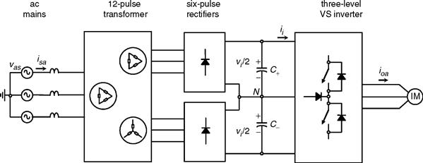
FIGURE 15.63 ASD based on a three-phase three-level VSI topology.
This approach cannot be used when the inverter does not feature dc link voltage supplies. This is the case of static power reactive power compensators and static power active filters. In this case, the proper gating of the power valves becomes the only choice to keep and balance the dc link voltages. Figure 15.64a shows this case where the current added by the inverter ioabc provides the reactive power and current harmonics such that the ac mains current isabc features a given power factor.
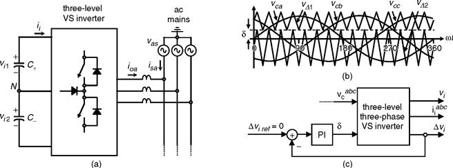
FIGURE 15.64 Reactive power and current harmonics compensator based on a three-phase three-level VSI topology: (a) power topology; (b) carrier and modulating signals; and (c) δ closed loop scheme.
The SPWM modulating technique could be used as in Fig. 15.60; however, the zero level of the carriers δ is left as a manipulable variable Fig. 15.64b. In fact, it is used to control the difference of the upper and lower capacitor voltages Δvi = vi1 — vi2. A closed loop alternative is depicted in Fig. 15.64c to manipulate δ. The modulating signals vcabc are left to control the reactive power and current harmonics injected into the ac mains by regulating the currents ioabc and keep the total dc link voltage vi = vi1 + vi2 equal to a reference. Both loops are not included in Fig. 15.64c.
15.7.3 Current Source-based Multilevel Topologies
Duality is found in many aspects related to voltage and current source inverters. Perhaps, the most evident is the duality in terms of modulating techniques. Thus, current source based multilevel topologies are available as well. As expected, all the benefits and all the drawbacks found in voltage source topologies should be found in current source topologies.
Figure 15.65 shows a three-level N = 3 current source topology, which is formed by paralleling two standard six-switches topologies. The main goal is to share evenly the ac current ioabc among the two topologies (ioabc/2 = ioabc1 = ioabc2) This should be ensured by having equal dc link currents (ii1 = ii2) Similarly to voltages source based mutlilevel topologies, this could be achieved by using either two independent dc link currents or by properly gating the power valves. Both alternatives are reviewed later on.
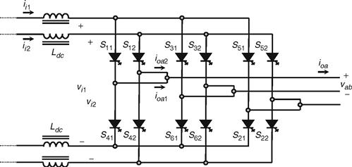
FIGURE 15.65 Three-phase three-level CSI topology.
A. The SPWM Technique in Three-level CSIs
As in three-level VSIs, the main objective is to generate the appropriate 12 gating signals so as to obtain fundamental inverter line currents equal to a given set of modulating signals. Specifically, the SPWM in three-level inverters uses a sinusoidal set of modulating signals (ica, icb, and icc for phases a, b, and c, respectively) and N − 1 = 2 triangular type of carrier signals (iΔ 1 and iΔ 2) as illustrated in Fig. 15.66a and 15.66e. The best results are obtained if the carrier signals are 180° out of phase and feature an odd normalized frequency (e.g. mf = 15). In order to use the same set of carrier signals to generate the gating signals for phases b and c, the normalized frequency of the carrier signal mf should be a multiple of 3. Thus, the possible values are mf = 3,9,15,21,. …
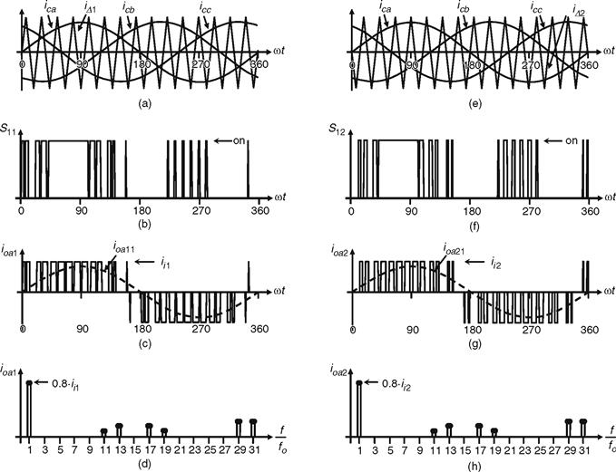
FIGURE 15.66 Three-level CSI topology. Relevant waveforms using a SPWM (mf = 15, ma = 0.8): (a) modulating signals and carrier signal 1; (b) switch Si i status; (c) inverter 1 linea current; (d) inverter 1 linea current spectrum; (e) modulating signals and carrier signal 2; (f) switch S12 status; (g) inverter 2 linea current; and (h) inverter 2 linea current spectrum.
Figure 15.66 shows the relevant waveforms for a three-level inverter modulated by means of a SPWM technique (mf = 15, ma = 0.8). Specifically, Fig. 15.66b and 15.66f show the gating signals obtained as described earlier in this chapter. The inverter line currents shown in 15.66c and 15.66g feature spectra shown in 15.66d and 15.66h, respectively. As expected, the inverter line currents contain harmonics at l · mf ± k with l = 1,3,… and k = 2,4,… and at l (mf ± k with l = 2,4,. and k = 1,3,. … For instance, the first set of harmonics in the line currents (l = 1, mf = 15) are at 15 ± 2, 15 ± 4,. …
The total inverter line current is shown in Fig. 15.67a, and features the first set of unwanted harmonics around 2 mf Fig. 15.67b. This becomes the first advantage of using a multilevel topology as the filtering component requirements become more relaxed. All the other features of carrier-based PWM techniques also apply in current source multilevel inverters. For instance: (I) the fundamental component of the line currents satisfy
![]() (15.94)
(15.94)
where 0 < ma ≤ 1 is the linear operating region. Also: (II) to further increase the amplitude of the load currents, a zero sequence signal could be injected to the modulating signals, in this case
![]() (15.95)
(15.95)
the overmodulation operating region can be used by further increasing the modulating signal amplitudes ![]() , where the line currents range in
, where the line currents range in
![]() (15.96)
(15.96)
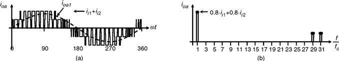
FIGURE 15.67 Three-level CSI topology. Relevant waveforms using a SPWM (mf = 15, ma = 0.8): (a) total inverter line current and (b) total inverter line current spectrum.
Also: (III) a nonsinusoidal set of modulating signals could also be used by the modulating technique. This is the case where nonsinusoidal line currents are required as in active filter applications; and (IV) because of the two quadrants operation of CSIs, the multilevel inverter could equally be used in applications where the active power flow goes from the dc to the ac side or from the ac to the dc side. In general, for an N-level inverter modulated by means of a carrier-based technique, three modulating signals 120° out-of-phase and N − 1 carrier signals are required and the line currents in the inverters have a peak value of ii/(N − 1).
One of the drawbacks of the multilevel inverter is that the dc link capacitors cannot be supplied by a single dc voltage source. This is due to the fact that the currents required by the inverter in the dc bus are not symmetrical and therefore the capacitors will not equally share the dc supply voltage vi. To overcome this problem, two alternatives are developed later on.
B. DC Link Voltage Balancing Issues
Figure 15.65 shows a three-level inverter and the ideal waveforms are shown in Fig. 15.66 and Fig. 15.67, which assume equal dc link currents, ii1 = ii2 This even distribution is not naturally achieved and could be overcome by supplying the dc link inductors from independent supplies or properly gating the power valves of the inverter in order to minimize the unbalance.
Figure 15.68 shows an ASD based on a three-level current source inverter, where the dc link inductors are feed from two different sources. Unlike the VS topology, the scheme needs a closed loop control strategy to keep constant the dc link currents and equal to a given reference. This is achieved in commercial units by using either phase-controlled rectifiers or PWM rectifiers. Nevertheless, the multipulse transformer required to provide isolated dc link currents improves the ac mains current as in the VS multilevel topology.
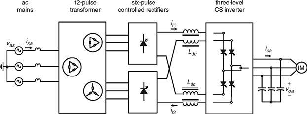
FIGURE 15.68 ASD based on a three-phase three-level CSI topology.
This approach cannot be used when the inverter is not feed from an external power supply. This is the case of static series voltage compensators. In this case, the proper gating of the power valves becomes the only choice to keep and balance the dc link currents. Figure 15.64a shows this case where the voltage added by the inverter n voabc compensates the sags and/or swells present in the ac mains in order to provide a constant voltage to the load.
The SPWM modulating technique could be used as in Fig. 15.66 and Fig. 15.67; however, the peak amplitude of one triangular is amplified in the factor 1 + δ and the peak amplitude of other triangular is amplified in the factor 1 − δ, where δ is left as a manipulable variable Fig. 15.69b. In fact, δ is used to control the difference of the dc link currents Δii = ii1 –ii2.
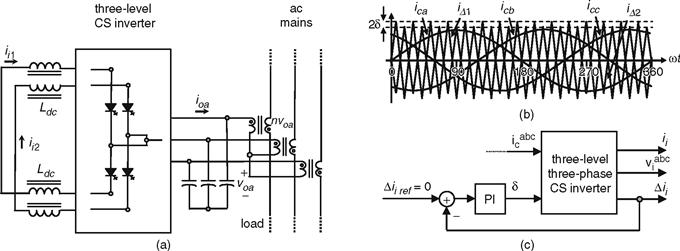
FIGURE 15.69 Reactive power and current harmonics compensator based on a three-phase three-level VSI topology: (a) power topology; (b) carrier and modulating signals; and (c) δ closed loop scheme.
A closed loop alternative is depicted in Fig. 15.69c to manipulate δ. The modulating signals icabc are left to control the series injected voltage into the ac mains by regulating the voltages voabc and keep the total dc link current ii = ii1 + ii2 equal to a reference. Both loops are not included in Fig. 15.69c.
Acknowledgment
The author is grateful for the financial support from the Chilean Fund for Scientific and Technological Development (FONDECYT) through project 105 0958.
Further Reading
Inverters Applications
1. Huang Chih-Yi, Wei Chao-Peng, Yu Jung-Tai, Hu Yeu-Jent. Torque and current control of induction motor drives for inverter switching frequency reduction. IEEE Trans. Industrial Electronics. 2005; 52(5):1364–1371.
2. Rodriguez J, Moran L, Pontt J, Espinoza J, Diaz R, Silva E. Operating experience of shovel drives for mining applications. IEEE Trans. Industry Applications. 2004; 40(2):664–671.
3. Espinoza J, Morán L, Guzmán J. Multi-level three-phase current source inverter based AC drive for high performance applications. Conf. Rec. PESC’ 05. June 2005.
4. Joós G, Espinoza J. Three phase series var compensation based on a voltage controlled current source inverter with supplemental modulation index control. IEEE Trans. Power Electronics. 1999; 15(3):587–598.
5. Jain P, Espinoza J, Jin H. Performance of a single-stage UPS system for single-phase trapezoidal-shaped ac voltage supplies. IEEE Trans. Power Electronics. 1998; 13(5):912–923.
6. Akagi H. The state-of-the-art of power electronics in Japan. IEEE Trans. Power Electronics. 1998; 13(2):345–356.
7. Wu T, Yu T. Off-line applications with single-stage converters. IEEE Trans. Industry Applications. 1997; 44(5):638–647.
8. Akagi H. New trends in active filters for power conditioning. IEEE Trans. Industry Applications. 1996; 32(6):1312–1322.
9. Espinoza J, Joós G. A current source inverter induction motor drive system with reduced losses. IEEE Trans. Industry Applications. 1998; 34(4):796–805.
10. Ryan M, Brumsickle W, Lorenz R. Control topology options for single-phase UPS inverters. IEEE Trans. Industry Applications. 1997; 33(2):493–501.
11. Jungreis A, Kelly A. Adjustable speed drive for residential applications. IEEE Trans. Industry Applications. 1995; 31(6):1315–1322.
12. Rajashekara K. History of electrical vehicles in General Motors. IEEE Trans. Industry Applications. 1994; 30(4):897–904.
13. Bose B. Power electronics and motion control –Technology status and recent trends. IEEE Trans. Industry Applications. 1993; 29(5):902–909.
14. Bhowmik S, Spée R. A guide to the application-oriented selection of ac/ac converter topologies. IEEE Trans. Power Electronics. 1993; 8(2):156–163.
Current Source Inverters
15. Espinoza J, Morán L, Zargari N. Multi-level three-phase current source inverter based series voltage compensator. Conf. Rec. PESC’ 05. 2005.
16. Pande M, Jin H, Joós G. Modulated integral control technique for compensating switch delays and nonideal dc buses in voltage-source inverters. IEEE Trans. Industrial Electronics. 1997; 44(2):182–190.
17. Espinoza J, Joós G. Current-source converter on-line pattern generator switching frequency minimization. IEEE Trans. Industry Applications. 1997; 44(2):198–206.
18. Joós G, Moschopoulos G, Ziogas P. A high performance current source inverter. IEEE Trans. Power Electronics. 1993; 8(4):571–579.
19. Chiang Loh Poh, Holmes DG. Analysis of multiloop control strategies for LC/CL/LCL-filtered voltage-source and current-source inverters. IEEE Trans. Industry Applications. 2005; 41(2):644–654.
20. Salo M, Tuusa H. Vector-controlled PWM current-source-inverter-fed induction motor drive with a new stator current control method. IEEE Trans. Industrial Electronics. 2005; 52(2):523–531.
21. Shen Dong, Lehn PW. Modeling, analysis, and control of a current source inverter-based STATCOM. IEEE Trans. on Power Delivery. 2002; 17(1):248–253.
22. Bendre A, Wallace I, Nord J, Venkataramanan G. A current source PWM inverter with actively commutated SCRs. IEEE Trans. Power Electronics. 2002; 17(4):461–468.
23. Han BM, Moon SI. Static reactive-power compensator using soft-switching current-source inverter. IEEE Trans. Industrial Electronics. 2001; 48(6):1158–1165.
24. Zmood DN, Holmes DG. Improved voltage regulation for current-source inverters. IEEE Trans. Industry Applications. 2001; 37(4):1028–1036.
Modulating Techniques and Control Strategies25. Espinoza J, Joós G. DSP implementation of output voltage reconstruction in CSI based converters. IEEE Trans. Industrial Electronics. 1998; 45(6):895–904.
26. Kazmierkowski M, Malesani L. Current control techniques for three-phase voltage-source PWM converters: A survey. IEEE Trans. Industrial Electronics. 1998; 45(5):691–703.
27. Tilli A, Tonielli A. Sequential design of hysteresis current controller for three-phase inverter. IEEE Trans. Industrial Electronics. 1998; 45(5):771–781.
28. Chung D, Kim J, Sul S. Unified voltage modulation technique for real-time three-phase power conversion. IEEE Trans. Industry Applications. 1998; 34(2):374–380.
29. Malesani L, Mattavelli P, Tomasin P. Improved constant-frequency hysteresis current control of VSI inverters with simple feed-forward bandwidth prediction. IEEE Trans. Industry Applications. 1997; 33(5):1194–1202.
30. Rahman M, Radwin T, Osheiba A, Lashine A. Analysis of current controllers for voltage-source inverter. IEEE Trans. Industrial Electronics. 1997; 44(4):477–485.
31. Trzynadlowski A, Kirlin R, Legowski S. Space vector PWM technique with minimum switching losses and a variable pulse rate. IEEE Trans. Industrial Electronics. 1997; 44(2):173–181.
32. Tadakuma S, Tanaka S, Naitoh H, Shimane K. Improvement of robustness of vector-controlled induction motors using feedforward and feedback control. IEEE Trans. Power Electronics. 1997; 12(2):221–227.
33. Holtz J, Beyer B. Fast current trajectory tracking control based on synchronous optimal pulse width modulation. IEEE Trans. Industry Applications. 1995; 31(5):1110–1120.
34. Espinoza J, Joós G, Ziogas P. Voltage controlled current source inverters. Conf. Rec. IECON’ 92. 1992; 512–517 [November].
35. Wang Fei. Sine-triangle versus space-vector modulation for three-level PWM voltage-source inverters. IEEE Trans. Industry Applications. 2002; 38(2):500–506.
36. Tse KK, Shu-Hung Chung Henry, Ron Hui SY, So HC. A comparative study of carrier-frequency modulation techniques for conducted EMI suppression in PWM converters. IEEE Trans. Industrial Electronics. 2002; 49(3):618–627.
37. Shi KL, Li H. Optimized PWM strategy based on genetic algorithms. IEEE Trans. Industrial Electronics. 2005; 52(5):1558–1561.
Overmodulation
38. Hava A, Sul S, Kerkman R, Lipo T. Dynamic overmodulation characteristics of triangle intersection PWM methods. IEEE Trans. Industry Applications. 1999; 35(4):896–907.
39. Hava A, Kerkman R, Lipo T. Carrier-based PWM-VSI overmodulation strategies: Analysis, comparison, and design. IEEE Trans. Power Electronics. 1998; 13(4):674–689.
40. Bae Bon-Ho, Sul Seung-Ki. A novel dynamic overmodulation strategy for fast torque control of high-saliency-ratio AC motor. IEEE Trans. Industry Applications. 2005; 41(4):1013–1019.
41. Park Hee-Jhung, Youn Myung-Joong. A new time-domain discontinuous space-vector PWM technique in overmodulation region. IEEE Trans. Industrial Electronics. 2003; 50(2):349–355.
42. Mondal SK, Bose BK, Oleschuk V, Pinto JOP. Space vector pulse width modulation of three-level inverter extending operation into overmodulation region. IEEE Trans. Power Electronics. 2003; 18(2):604–611.
43. Khambadkone AM, Holtz J. Compensated synchronous PI current controller in overmodulation range and six-step operation of space-vector-modulation-based vector-controlled drives. IEEE Trans. Industrial Electronics. 2002; 49(3):574–580.
44. Narayanan G, Ranganathan VT. Extension of operation of space vector PWM strategies with low switching frequencies using different overmodulation algorithms. IEEE Trans. Power Electronics. 2002; 17(5):788–798.
45. Bakhshai AR, Joos G, Jain PK, Jin Hua. Incorporating the overmodulation range in space vector pattern generators using a classification algorithm. IEEE Trans. Power Electronics. 2000; 15(1):83–91.
Selective Harmonic Elimination
46. Bowe S, Grewal S. Novel space-vector-based harmonic elimination inverter control. IEEE Trans. Industry Applications. 2000; 36(2):549–557.
47. Li L, Czarkowski D, Liu Y, Pillay P. Multilevel selective harmonic elimination PWM technique in series-connected voltage inverters. IEEE Trans. Industry Applications. 2000; 36(1):160–170.
48. Karshenas H, Kojori H, Dewan S. Generalized techniques of selective harmonic elimination and current control in current source inverters/converters. IEEE Trans. Power Electronics. 1995; 10(5):566–573.
49. Patel H, Hoft R. Generalized techniques of harmonic elimination and voltage control in thyristor inverters, Part I-Harmonic elimination. IEEE Trans. Industry Applications. 1973;IA-9(3):310–317.
50. Wells JR, Nee BM, Chapman PL, Krein PT. Selective harmonic control: a general problem formulation and selected solutions. IEEE Trans. Power Electronics. 2005; 20(6):1337–1345.
51. Newman MJ, Holmes DG, Nielsen JG, Blaabjerg F. A dynamic voltage restorer (DVR) with selective harmonic compensation at medium voltage level. IEEE Trans. Industry Applications. 2005; 41(6):1744–1753.
52. Espinoza JR, Joos G, Guzman JI, Moran LA, Burgos RP. Selective harmonic elimination and current/voltage control in current/voltage-source topologies: a unified approach. IEEE Trans. Industrial Electronics. 2001; 48(1):71–81.
Effects of PWM-type of Voltage Waveforms
53. Aoki N, Satoh K, Nabae A. Damping circuit to suppress motor terminal overvoltage and ringing in PWM inverter-fed ac motor drive systems with long motor leads. IEEE Trans. Industry Applications. 1999; 35(5):1015–1020.
54. Rendusara D, Enjeti P. An improved inverter output filter configuration reduces common and differential modes dv/dt at the motor terminals in PWM drive systems. IEEE Trans. Power Electronics. 1998; 13(6):1135–1153.
55. Chen S, Lipo T. Bearing currents and shaft voltages of an induction motor under hard- and soft-switching inverter excitation. IEEE Trans. Industry Applications. 1998; 34(5):1042–1048.
56. von Jouanne A, Zhang H, Wallace A. An evaluation of mitigation techniques for bearing currents, EMI and overvoltages in ASD applications. IEEE Trans. Industry Applications. 1998; 34(5):1113–1122.
57. Akagi H, Doumoto T. A passive EMI filter for preventing high-frequency leakage current from flowing through the grounded inverter heat sink of an adjustable-speed motor drive system. IEEE Trans. Industry Applications. 2005; 41(5):1215–1223.
Multilevel Structures
58. Tolbert L, Habetler T. Novel multilevel inverter carrier-based PWM method. IEEE Trans. Industry Applications. 1999; 35(5):1098–1107.
59. Walker G, Ledwich G. Bandwidth considerations for multilevel converters. IEEE Trans. Power Electronics. 1999; 15(1):74–81.
60. Liang Y, Nwankpa C. A new type of STATCOM based on cascading voltage-source inverters with phase-shifted unipolar SPWM. IEEE Trans. Industry Applications. 1999; 35(5):1118–1123.
61. Schibli N, Nguyen T, Rufer A. A three-phase multilevel converter for high-power induction motors. IEEE Trans. Power Electronics. 1998; 13(5):978–986.
62. Lai J, Peng F. Multilevel converters –A new breed of power converters. IEEE Trans. Industry Applications. 1997; 32(3):509–517.
63. Tallam RM, Naik R, Nondahl TA. A carrier-based PWM scheme for neutral-point voltage balancing in three-level inverters. IEEE Trans. Industry Applications. 2005; 41(6):1734–1743.
64. Perez MA, Espinoza JR, Rodriguez JR, Lezana P. Regenerative medium-voltage AC drive based on a multicell arrangement with reduced energy storage requirements. IEEE Trans. Industrial Electronics. 2005; 52(1):171–180.
Regeneration
65. Verdelho P, Marques G. DC voltage control and stability analysis of PWM-voltage-type reversible rectifiers. IEEE Trans. Industrial Electronics. 1998; 45(2):263–273.
66. Espinoza J, Joós G, Bakhshai A. Non-linear control and stabilization of PWM current source rectifiers in the regeneration mode. Conf. Rec. APEC’ 97. 1997; 902–908 [February].
67. Hinkkanen M, Luomi J. Stabilization of regenerating-mode operation in sensorless induction motor drives by full-order flux observer design. IEEE Transaction on Industrial Electronics. 2004; 51(6):1318–1328.
68. Tanaka T, Fujikawa S, Funabiki S. A new method of damping harmonic resonance at the DC link in large-capacity rectifier-inverter systems using a novel regenerating scheme. IEEE Trans. Industry Applications. 2002; 38(4):1131–1138.
69. Rodriguez J, Pontt J, Silva E, Espinoza J, Perez M. Topologies for regenerative cascaded multilevel inverters. Conf. Rec. PESC’ 03. 2003; 519–524 [June].