
20
Gate Drive Circuitry for Power Converters
Tech Eng, MSc University of Cape Town, Department of Electrical Engineering, Cape Town, South Africa
20.1 Introduction to Gate Drive Circuitry
20.2 Semiconductor Drive Requirements
20.2.1 Current-driven Devices
20.2.2 Voltage-controlled Devices
20.3 Gate Drivers for Power Converters
20.3.1 Floating Supply
20.3.2 Level Shifting
20.4 Gate Driver Circuit Implementation
20.4.1 Isolated Gate Drivers
20.4.2 Electronic Gate Drivers
20.5 Current Technologies
20.5.1 Transformer Coupled Isolated Drivers
20.5.2 Non-isolated Electronic Level Shifted Drivers
20.5.3 High-speed Gate Drivers
20.5.4 Resonant Gate Drivers
20.6 Current and Future Trends
20.7 Summary
20.1 Introduction to Gate Drive Circuitry
Global trends towards energy efficiency over the last three decades has facilitated the need for technological advancements in the design and control of power electronic converters for energy processing. These power electronic converters find widespread applications in industry such as:
Consumer electronics
Automobile industries
Commercial sectors
• Variable speed motor drives for conveyor belt systems
• Induction heating installations for metals processing
Domestic electronics
• Fluorescent, compact fluorescent, and incandescent lighting, washing machines, cooking appliances, and dish washers
Utility applications
All of the above applications utilize similar power converter topologies. This allows for controlled and efficient power conversion from one form of energy to another, utilizing semiconductor technologies such as BJT transistors, SCRs (thyristors), IGBTs, and power MOSFETs.
It is true that “Power is nothing without control” (Pirelli Tyres). The gate drive circuitry of a power converter forms an important interface between the high power electronics and the intelligent control processing stages.
It is therefore of utmost importance that this interface between the control and power electronics is well designed, since it can have a substantial impact on the performance and reliability of a power electronic system. (See Fig. 20.1.)
![]()
FIGURE 20.1 Generalized layout of a power electronic system showing the situation of the gate driver circuits.
20.2 Semiconductor Drive Requirements
Power semiconductor devices have three operating states commonly known as the cut-off mode, the active mode, and the saturation mode. In power electronic converters which utilize switch-mode operation, the aim is to operate these semiconductors in either the cut-off region or the saturation region, whilst making the transition through the active or linear region as short as possible in order to facilitate maximum power conversion efficiency. In order to achieve these fast transition times, a suitable gate driver circuit is required. This gate driver has to be able to supply the necessary charge to the power semiconductor device gate junction in order to achieve turn-on and turn-off.
Power semiconductors can be classified into two categories with respect to drive requirements, namely: current-driven devices and voltage-driven devices.
20.2.1 Current-driven Devices
A current-driven device is a device that requires a constant current drive for a period of time in order to initiate and/or remain in conduction. Two popular types of current controlled devices are the bipolar power transistor and the thyristor (SCRs). The SCR is mainly used in AC–DC converters such as controlled rectifiers where the input AC voltage helps to commutate (turn-off) the devices by polarity reversal. In DC–AC inverters, the gate turn-off thyristors (GTOs) are generally used due to their ability to be both turned on and off by a gate control signal. This eliminates the need for forced commutation circuitry, needed to turn-off the thyristor in these applications due to the absence of a reversing polarity AC input voltage. Thyristors and GTOs still dominate the high voltage and high current applications, like DC transmission, requiring converters up to the megawatt range. The evolution of the IGBT power semiconductor device has resulted in thyristors and GTOs being used less in conventional power converters these days. IGBTs are readily available with on-state currents of several hundred amperes and blocking voltages in excess of 1.7 kV. The IBGTs offer much faster switching speeds than thyristors and have much lower gate drive power requirements than SCRs or power bipolar junction transistors (BJT). The IGBTs have already replaced power BJTs in most applications due to their superior performance. The next generation of silicon carbide technology could realize IGBT devices with blocking voltages in excess of 4 kV and may one day even replace SCR and GTO devices completely.
20.2.2 Voltage-controlled Devices
These devices are semiconductors which require a constant voltage drive on the gate control terminal in order to remain in conduction. The input drive requirements of these devices are substantially lower than their current-driven counterparts and are the preferred choice in modern power electronics. Two such devices are the power MOSFET and the IGBT which are forced commutated switching devices being fully controlled at the gate terminal under normal operating conditions. These devices do not latch into conduction, and therefore do not require special commutation circuits. The gate input junction of a MOSFET and IGBT is purely capacitive, so, no gate drive current is needed in the steady state, unlike transistors. A minimum gate drive voltage however must be maintained (above the gate threshold voltage) at the device gate in order for it to remain in conduction. A high current low impedance drive circuit is needed to inject, or remove current, from the gate at high slew rates in order to switch the device rapidly. The gate drain capacitance, although small, can also require significant charge as at high drain voltage slew rates (the Miller effect) [1].
The process of supplying the necessary power for the efficient driving of voltage-controlled devices is an ongoing area of research. This chapter will however only focus on the gate driver circuitry required to drive power MOSFETs and IGBTs in the bridge circuit configuration. The basic symbolic representation of the power MOSFET and IGBT is shown below. Figure 20.2 represents the static model of these devices. Unlike the power MOSFET, the IGBT can be manufactured without the integral body diode. Often power MOSFETs are represented as shown below, omitting the integral body diode which is always present in the MOSFET device. Care should be taken when reading circuits, not to forget this extra unseen component.
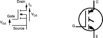
FIGURE 20.2 Static model representation of the power MOSFET and IGBT power semiconductor devices.
The dynamic model for a power MOSFET is shown in Fig. 20.3 [1, 2]. It can be noted that the integral body diode situated in the power MOSFET structure is actually a parasitic bipolar transistor. This parasitic element is the result of a fabrication process used when manufacturing power MOSFETs. The base of the BJT is usually floating, and a pull down resistor Rbe is included in the chip structure in order to keep the BJT base shorted to the MOSFET source terminal at all times. This is very necessary, since a floating BJT base will result in uncontrolled turn-on of the BJT device. By shorting the BJT base to the MOSFET's source terminal, a diode structure is now created, yielding the dynamic model with the integral body diode formed by the BJT base collector junction as shown in Fig. 20.3 [1, 2]. The turn-on of the BJT element during transients substantially degrades the performance of the power MOSFET. When the MOSFET is exposed to a fast changing transient voltage (dv/dt) across its drain to source terminals, enough current flows in Rbe, thereby biasing the parasitic bipolar into conduction. This transient can occur during the turn-on or turn-off of the device. To avoid transient susceptibility, the device dv/dt rating must be adhered to at all times. The input capacitance of the power MOSFET comprises the gate to source capacitance (Cgs) and the gate to drain capacitance (Cgd) also known as the Miller capacitance. The input gate structure for the IGBT is essentially the same as for the power MOSFET. A gate driver must be capable of supplying sufficient charge to both Cgs and Cgd when switching power MOSFETs and IGBTs in power converters.
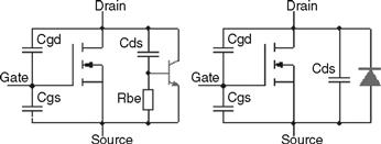
FIGURE 20.3 A dynamic model of the power MOSFET shows the presence of the parasitic BJT element found in the MOSFET structure [1, 2].
A dynamic model of the IGBT is shown in Fig. 20.4. The IGBTs are essentially bipolar devices like BJTs with a MOSFET structured high impedance input. A parasitic transistor is also found in the IGBT chip structure as part of the manufacturing process. Combined with existing bipolar power transistor, it forms a parasitic thyristor, which once latched into conduction device, turn-off is not possible via the gate terminal. To avoid this uncontrolled behavior, the maximum allowable peak current and dv/dt ratings of the device must be adhered to at all times [1].
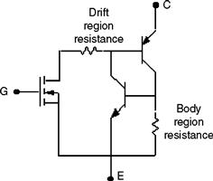
FIGURE 20.4 Dynamic model of an IGBT showing the location of the parasitic thyristor responsible for uncontrolled device latch up [1].
Both MOSFETs and IGBTs require sufficient charge deposited into their gate junctions, whilst maintaining a minimum gate threshold voltage in order to remain in conduction. When designing a gate driver, it is always important to understand both the static and dynamic behavior of the semiconductor device used as it aids the effectiveness of the design for a given gate driver system.
20.3 Gate Drivers for Power Converters
Power electronic converters are found in various configurations. Each has a complex switching function with the goal of achieving efficient power conversion. These converters make use of various floating potentials in order to achieve an AC or quasi-DC output characteristics. Gate drivers function as current buffers and signal converters. They convey both the switching state information and gate drive power required during the power semiconductor switching process.
20.3.1 Floating Supply
Power converters employing bridge configurations function by virtue of a high-side switch as shown in Fig. 20.5 below.
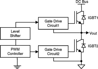
FIGURE 20.5 Simple structure of a bridge topology and driving circuit illustrating the concept of a high-side switch.
In order to drive a device like an IGBT or power MOS–FET into conduction, the gate terminal must be made positive with respect to its source or emitter. A common misconception made by many newcomers to the field of power electronics is that, because the emitter or source terminal is usually at some ground potential, it must be made positive with respect to ground. It can be noted that the emitter terminal of IGBT1, in the circuit above, can be floating anywhere from ground up to the DC bus potential, depending on the operating states of IGBT1 and IGBT2, and is therefore not referenced to the system ground potential. A supply is therefore needed in order to provide power to any circuitry associated with this floating midpoint potential. This type of supply is commonly referred to as a floating supply. Three of the most common methods of generating a floating supply are described next.
• Isolated SupplyThe simplest way of generating a floating supply is to use a transformer isolated supply. Compared to other methods, this type of supply is able to supply a continuous, large amount of current. A mains frequency transformer supply is cheap, but is usually very bulky. By employing a high frequency isolated DC–DC converter, fed from an existing DC supply, an isolated floating supply can be generated employing a much smaller isolation transformer.
• Charge-pump SupplyThe charge-pump technique superimposes the voltage of one supply onto another. It is normally used for generating a boost voltage on top of the main high-voltage supply. The charge-pump supply is not suitable for generating a boost voltage for powering floating high-side circuitry. A benefit of employing the charge-pump technique is that a continuous supply to the circuit is maintained. Due to complexity and cost, this circuit is not commonly used for power converters [3, 4].
• Bootstrap SupplyA very common technique employed to generate a floating supply, the bootstrap supply is a simple circuit using only one diode and a supply storage capacitor. This technique is commonly used for low cost solutions in converters up to several kilowatts. Typical applications include electronic ballasts and variable speed motor drives.
A simplified schematic of a bootstrap circuit is shown in Fig. 20.6. When the low-side switch M2 is on, the bootstrap diode, D, conducts and charges the storage capacitor. If we assume the saturation voltage drop of the low-side power device M2 and the forward volt drop of diode D to be negligible, the capacitor will charge to approximately the low voltage supply potential. When the high-side switch M1 is on low side switch M2 is off, D is reverse-biased and the high-side circuitry is powered from C. In this condition, the voltage on C droops as it discharges when supplying the high-side circuitry.
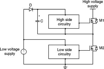
FIGURE 20.6 Bootstrap technique employed for creating a floating supply.
The amount of voltage droop is a function of the current drawn, the size of the capacitor, and the operating frequency of the converter [3]. Detailed design and application literature on bootstrap supplies can be found in [4].
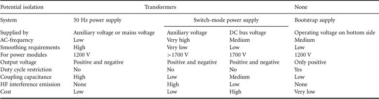
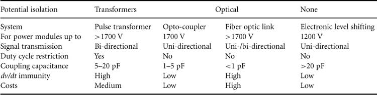
A summary and comparison of the various methods of generating a floating supply is given in Table 20.1 [5].
TABLE 20.1 Comparison of the various techniques of creating a gate driver floating supply [5]
20.3.2 Level Shifting
The second requirement for driving a high-side switch, is that the control signal fed from the PWM electronics needs to be conveyed to the floating driver circuitry. A level-shifting circuit is required in order to achieve this.
The GD1 and GD2 are the respective high- and low-side gate drive circuits. In order to signal the high-side gate driver circuitry to commence turn-on of the high-side IGBT switch, the control signal V1 which is referenced to the control circuit ground potential needs to be referenced to the floating potential Vout at the IGBT1 emitter. This implies that the control signal V1 will be level shifted to Vg1 as shown in Fig. 20.7. A level shifter can be thought of as an isolating black-box that transfers a signal across a potential barrier [6]. The maximum level attained by Vg1 will be Vout + V1. In power converters, operating off mains voltage, these levels can be in excess of 500 V. Level shifting is achieved in one of the following ways:
• Transformer Level ShiftingTransformers are an obvious choice for providing a level shifted signal. They have excellent noise immunity when compared to opto-couplers. Level shifting transformers also have the benefit of providing both the control and gate drive power signal to the power semiconductor switch (Fig. 20.8), thereby eliminating. This eliminates the need for a floating power supply. When operating at high switching frequencies, above several hundred kilohertz, careful transformer design has to be applied in order to avoid the adverse effects of transformer leakage inductance. Another limitation in the transformer gate driver, is when large currents are required at high speed for gate driving. The influence of the transformer parasitic components becomes significant. In the effort to deliver high peak currents at fast rise and fall times, the transformer turns are usually minimized, which leads to other transformer design limitations.To avoid degradation of the gate drive waveform in the case of high speed and high current delivery, it is sometimes better to convey only the low power control signal via a transformer and also to employ a dedicated low-impedance output MOS-gate driver with a floating power supply [3].A drawback of the gate drive transformer is that it cannot convey DC information (since the average volt–time product across any winding must be zero) and therefore has a limitation to its operation as shown in Fig. 20.9. When a high duty cycle is commanded, the gate drive capacitor will remove the DC offset in the signal, and could result in operation below the device threshold voltage Vge(th) as shown in Fig. 20.9c [3]. This condition will result in the device not turning on, or even operating in the linear region. This results in excessive semiconductor power dissipation.
• Optical Level Shifting –Opto-couplersOptical isolation is another technique used for achieving level shifting. The trade-off however, is that a separate floating supply is now required on the receiver end of the gate driver interface. Opto-couplers offer a cost effective, and easy solution, but are susceptible to noise and fast voltage transitions. This is common in gate drive circuits. This requirement places more demand on the power supply filtering and PCB layout around the opto-coupler in order to achieve reliable operation. Other benefits of opto-coupler technology is the small footprint (6-8 pin dual in line or surface mount package), output enable pin, and compatibility with any logic level input since its input is current-driven (an input diode). Commercially available opto-couplers cover a wide range of operating speeds of up to 15 MBd, with rise and fall times of 10–20 ns and noise immunity levels (dv/dt rating) of 10–15 V/ns. Typical opto-coupler isolation voltages are in the region of 5 kV which is sufficient, since most semiconductors have breakdown voltages lower than this.
• Optical Level Shifting –Fiber Optic LinkElectrical conductors are susceptible to electromagnetic fields, and hence will radiate and pick up electromagnetic noise. Fiber optic links neither emit, nor receive electromagnetic noise, and pass through noisy environments unaffected. In addition, when dealing with very rapidly changing currents, ground noise can become a problem. A fiber optic link practically eliminates any ground loop or common-mode noise problems. A basic fiber optic communication system is given in Fig. 20.10. The LED is driven by the PWM drive signal. The light emitted from the LED is sent down a length of fiber optic cable to the receiver. The receiver consists of a PIN photodiode and a trans-impedance amplifier. The output voltage of the amplifier is level detected by a comparator, and converted into a logic signal.The galvanic isolation and dv/dt rating of this communication link can be increased to almost any desired value by simply lengthening the fiber optic cable. For a modest length of 10 cm of fiber optic cable, the isolation voltage is approximately 100 kV. The dv/dt rating is difficult to calculate, but as the coupling capacitance is practically zero, even the highest realizable dv/dt rating will have little effect. The bandwidth available in fiber optics systems makes operation at over 1 GHz possible [7].
• Electronic Level ShiftingElectronic level shifters work on the principle of having a current source referenced to a fixed potential. This reference potential is usually that of the low-side switches source, hence they are also called common source level shifters. The drive signal causes a certain current to be drawn through a current source regardless of the voltage across it. The current is sensed by the receiving side and turned into on/off information. Electronic level shifters do not provide isolation, however being an all electronic solution, allows it to be integrated onto a single chip. A simple common source non-inverting level shifter is shown in Fig. 20.11. The output capacitance and the power dissipation by the current source, limit the frequency and voltage it can feasibly work at. A better solution, that decreases the amount of power dissipated, is to use a pulsed current source, which is then latched on the receiving side. Topologies such as the single-ended and dual current pulsed latch are discussed in detail in reference [3].
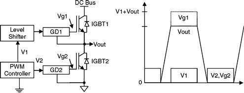
FIGURE 20.7 The concept of level shifting and the placement of the switching control signal on top of the inverter output voltage.
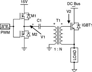
FIGURE 20.8 Combined transformer level shifter and gate driver. Capacitor C1 removes any DC offset in V1 thereby maintaining a zero average volt–time product across the transformer windings.
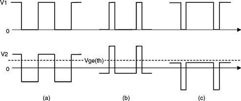
FIGURE 20.9 Operating waveforms for the pulse transformer circuit in Fig. 20.8 under different duty cycles.
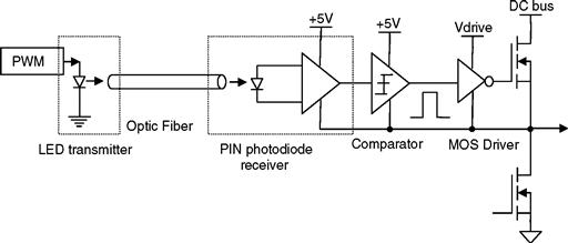
FIGURE 20.10 Fiber optic level shifting circuit used for high speed, extremely high noise immunity, and very high isolation voltage capability.
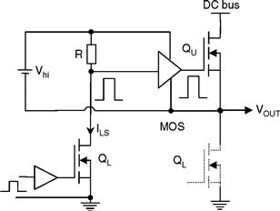
FIGURE 20.11 Electronic level shifting employed to convey the switching signal to the high-side gate drive circuitry. This technique does not offer any isolation but has widespread applications as an HV interface IC for power electronics applications.
A summary and comparison of the various methods of level shifting is given in Table 20.2 [5].
TABLE 20.2 Comparison of the various techniques of level shifting for gate drivers
20.4 Gate Driver Circuit Implementation
20.4.1 Isolated Gate Drivers
Gate driver circuits incorporating electrical isolation, provide the benefit of good noise interference immunity between power and control circuits. This is as a result of the separated ground return paths. Several types of isolated driver circuits exist namely:
• Isolated Power Supply with Opto-coupled Control Signal InputsA standard technique employed widely employed, is to generate floating supplies through the use of mains frequency transformer isolation (Fig. 20.12). Although not a very space-efficient solution (due to the mains frequency transformer size) compared to other methods, this technique is still well suited to almost any power electronic converter application. The power supply circuits can comprise standard low-voltage bridge rectifier modules. A regulated supply is easily realized using three-terminal voltage regulators, which can easily deliver continuous power to gate drive circuits in excess of 10 W. With each winding and its associated power supply, referenced to the IGBT or power MOSFET source, this system is a reliable and medium cost solution for almost any power converter up to switching frequencies well below 1 MHz. For higher operating frequencies, the inter-winding capacitance of the mains frequency transformer, leads to noise feed-through coupling. This causes spurious effects, like unscheduled turn-on of the power devices due to noise present in the driver circuit ground return path. The solution to this problem would then be to introduce a high frequency DC–DC converter, which incorporates a small HF isolation transformer with substantially reduced inter-winding capacitance.Level shifting of the switching control signal is achieved by means of optical isolation, (U3 and U4) with the input diodes (primary side of opto-coupler) referenced to the logic ground of the signal processing circuitry. The low impedance gate driver output is achieved by employing a high speed, high current buffer integrated circuit or a discrete bipolar or MOS complementary totem pole stage. Power to the opto-coupler and buffer U5 and U6 is derived from the respective floating power supply. The circuit above does not have any operating duty cycle limitations due to the floating power supply.The passive network comprising D1, R5, and R6 control the IGBT switching speed, and impacts on the performance and efficiency of the power converter. The R6 controls the turn-on switching speed of IGBT1. This controls the device switching loss as well as the turn-off dv/dt characteristics of the lower devices (IGBT2) free-wheeling diode for inductive loads. Diode D1 disconnects R5 from the circuit during the IGBT turn-on. The turn-off speed of IGBT1 is controlled by R5, provided that R5 is much smaller than R6. This is a desirable feature in voltage-fed inverters, since it ensures a minimum dead-time between device transitions as shown in Fig. 20.13.The U5out and U6out in Fig. 20.13 represent the driver output signal at exactly 50% duty cycle. The passive gate network on each IGBT, alters the drive signals due to the RC time constant formed between the gate drive resistors and the IGBT gate capacitance. This is shown as VgIGBT which is measured directly on the IGBT gate terminal. This slewing action on the IGBT gate results in the IGBT having a delayed turn-on. Turn-on occurs when the IGBT gate voltage reaches its threshold level (Vgth) and collector current starts to flow. The result is a dead-time created between switching transitions. This is required in any bridge circuit to avoid shoot through or cross-conduction of the upper and lower switches. This is depicted by the collector current trace (IC) for a purely resistive load in Fig. 20.13.
• Transformer Coupled Driver Supplying both Power and Control SignalsA transformer coupled gate driver is shown in Fig. 20.14. This system provides both the floating supply, as well as the level shifting of the switching signal. The push–pull driver on the primary side of the transformer T1, is used to supply a bi-directional current in the primary, without the use of a split power supply. The transformer T1 is rated for the PWM operating frequency, and can be realized by employing either a ferrite or iron powder core. The system operation is limited to a maximum PWM duty cycle of 50%. One of the benefits of this driver circuit, is its ability to generate a negative gate bias voltage when the device is off, due to transformer action. This feature is favorable since it reduces the IGBT dv/dt susceptibility by holding the gate terminal at a negative potential during turn-off transients, thereby avoiding uncontrolled turn-on or latch up in the IGBT. Back-to-back zener diodes placed across the gate-source terminal clamp the device gate voltage, thereby avoiding over voltages generated by the uncoupled transformer (T1) leakage inductance. The parallel resistor R5, acts as a gate pull down resistor holding the device in the off state during the initial power up of the gate driver circuit. The resistor –diode network in the gate drive circuit, (consisting of D1, R1, and R2) serves the same purpose as described in Fig. 20.12. The second function of this passive resistor network, is to dampen ringing effects. This is caused by the interaction between the IGBT or power MOSFET gate capacitance, and the gate drive transformer leakage inductance.
• Transformer Coupled Gate Driver with Large Duty Cycle CapabilityTransformers offer excellent noise immunity and provide simple and cost-effective gate drive solutions, whilst maintaining electrical isolation between the control and gate drive electronics. A drawback however is the limitation the transformer places on the maximum operating duty cycle. Figure 20.15 offers a simple but effective solution to the conventional limitations by the introduction of a DC restorer circuit which is formed by C2, Dz1, and Dz2. This system allows for removal of any DC information via C1, and restores the input waveform applied with the addition of a negative voltage bias needed for the IGBT gate drive. A small ferrite transformer core can be used for a MOSFET gate driver operational to several hundred kilohertz. This circuit can be redesigned for bridge topologies, but is also well suited for high voltage DC–DC converters requiring a high-side switch. The effective duty cycle range of this driver is from 5 to 95%. Operating waveforms are shown in Fig. 20.16.It should be noted that the gate drive voltage is clamped at fixed levels regardless of the duty cycle used, unlike the case in Fig. 20.9. This technique also supplies both the level shifted signal as well as the gate drive power, eliminating the need for an additional floating supply. The transformer turns ratio (T1) can also be adjusted to allow the circuit in Fig. 20.15 to operate from a 5V supply, whilst generating an output voltage swing from + 15 to –5V at the IGBT gate.
• Transformer Coupled Signal Modulated Gate DriverThe circuit in Fig. 20.17 employs a high-frequency carrier signal that is modulated by a lower frequency control signal (PWM). This is used to generate on/off switching instants of power IGBT1. By employing a high-frequency carrier, the transformer size is reduced, and by modulating the time in which the carrier operates, it controls the energy delivered to the gate of the IGBT. A carrier frequency for VSQ1 should be chosen to be much higher than the frequency of the PWM control signal. When the PWM control signal is enabled, the carrier signal is transformed to the secondary of transformer T1, which is rectified and filtered to produce a DC signal Vout.When the PWM control signal goes from the on- to the off-state, the charge stored in the filter capacitor C1 discharges by a time constant determined by R1. This is sometimes problematic when fast switching times are required, especially in inverter bridge configurations. A solution to this problem is to employ an active driver (U1) on the secondary side of the transformer. This will detect the carrier, and switch the IGBT gate accordingly. Operating waveforms for this circuit is shown in Fig. 20.18 [1].
• High Frequency Floating Power SupplyOften gate driver systems require extra electronics which has to be referenced to the floating switch being driven. Extra functional electronics often leads to higher power consumption, resulting in the need for a small low cost floating power supply as shown Fig. 20.19. The input section consisting of U1B, forms an oscillator used to drive a MOSFET at high frequency. This MOSFET drives a high-frequency transformer, which forms the isolation medium between the common auxiliary power supply and the floating secondary circuit. Transformer T1 produces a secondary output voltage which is rectified to form a floating DC supply for the associated gate drive circuitry. These floating power supplies are also available as monolithic DC–DC converter ICs with isolated outputs.
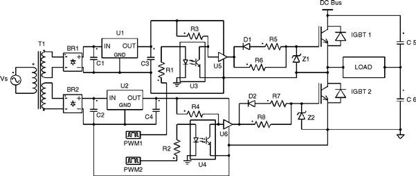
FIGURE 20.12 Mains frequency transformer employed to generate a floating supply. Simple and reliable, but larger than other solutions due to its mains frequency transformer. Works well for a half-bridge but would require more isolated power supplies if a full-bridge topology was employed. A 3-phase inverter would require either six separate floating supplies or three separate and one shared supply for the low-side devices.
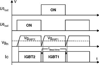
FIGURE 20.13 Switching waveforms for the circuit in Fig. 20.12.
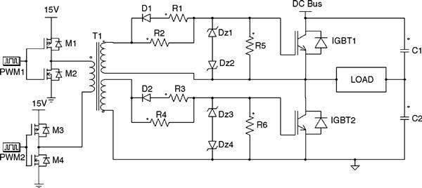
FIGURE 20.14 Transformer coupled gate driver used to supply both the control signal and the gate drive power to the device.
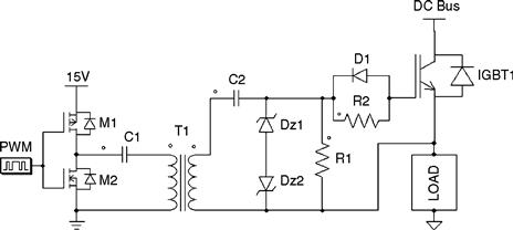
FIGURE 20.15 Transformer coupled gate driver with a large duty cycle operating range.
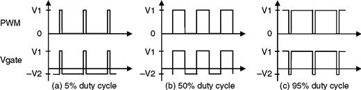
FIGURE 20.16 Operating waveforms of the transformer coupled gate driver in Fig. 20.15.
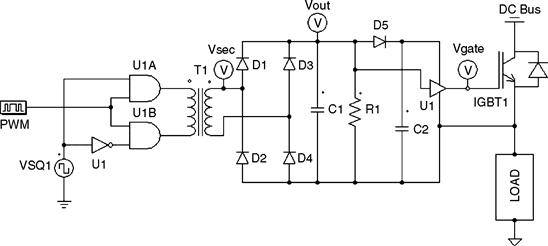
FIGURE 20.17 Signal modulated carrier used for level shifting and generation of a floating supply.
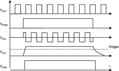
FIGURE 20.18 Signal modulated carrier used for level shifting and generation of a floating supply.
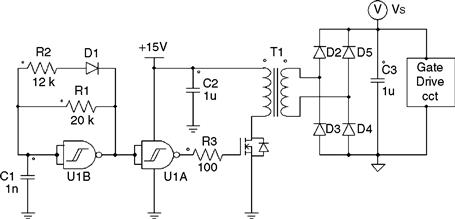
FIGURE 20.19 Low cost high frequency switch-mode floating supply.
20.4.2 Electronic Gate Drivers
These drivers utilize electronics in order to store energy in capacitors. This is used to produce floating referenced potentials. All circuits are referenced to a common ground potential. This technique provides a very cost-effective gate driver solution over the isolated versions, and are becoming increasingly popular in industries.
• Gate Driver with Bootstrapped Floating SupplyThe addition of a bootstrapped capacitor voltage allows for the generation of a floating supply in Fig. 20.20. Charging of C1 is achieved in the direction indicated during the period when MOSFET M2 is turned on. The turn-off of M2, results in the entrapment of charge in C1 which now acts as the power supply to OPTO1, U1, and the MOSFET M1's gate. As current is drawn from C1, the capacitor voltage tends to drop and needs to be replenished cyclically. The selection of the bootstrap capacitor value is critical for reliable operation of this circuit under extended duty cycle conditions. Diode D1 sees the full DC bus voltage when M2 is off, and therefore has to have a sufficiently high breakdown voltage. Applications with fast switching speed, require that D1 be a fast recovery diode in order to withstand the high dv/dt present across M2. Level shifting of the switching control signal is achieved by means of the opto-couplers in the circuit, providing the necessary control circuit isolation required.
• Gate Driver with Floating Supply Derived from DC BusWhen the generation of a floating supply is required without the need for isolation, the gate drive power can be derived from the DC bus voltage. The circuit is charged during the period when IGBT1 is off, with the gate drive energy stored in C2. The circuit connected to the enable pin of the opto-coupler, forms an under-voltage lockout which inhibits the IGBT drive signal at low DC supply voltages, typically during the initial start-up of the inverter circuit. The control signals are level shifted through an opto-coupler which drives a totem pole complimentary buffer stage as shown in Fig. 20.21 [8].

FIGURE 20.20 Optically isolated level shifter with an un-isolated bootstrapped floating supply derived from the low-side power supply.
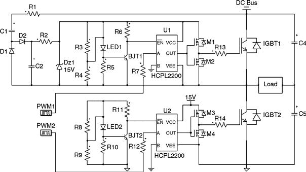
FIGURE 20.21 Level shifted gate driver with floating supply derived from the DC bus.
20.5 Current Technologies
The evolution of power semiconductor technology has led to the development of smart driver IC modules. These modules offer an essentially single chip/package solution to the gate driver designer, with the inclusion of minimal external components. These smart driver ICs utilize sophisticated electronics, yielding an intelligent gate driver in a small module. Some of these functions include the electronics for generating the floating supply from the auxiliary power supplied to the IC, level shifting with or without isolation. Advanced on-board integrated functions include under-voltage lockout, thermal trip, overload and de-saturation detection, soft start, and shutdown. These features enhance the effective utilization of the power converter and also increase its reliability.
20.5.1 Transformer Coupled Isolated Drivers
Semikron Corporation has developed a gate driver module that employs integrated floating supplies (Fig. 20.22) [9]. The level shifting is accomplished through transformer coupling, which is used as a bi-directional communications link for the transmission of the gate drive and fault signals.
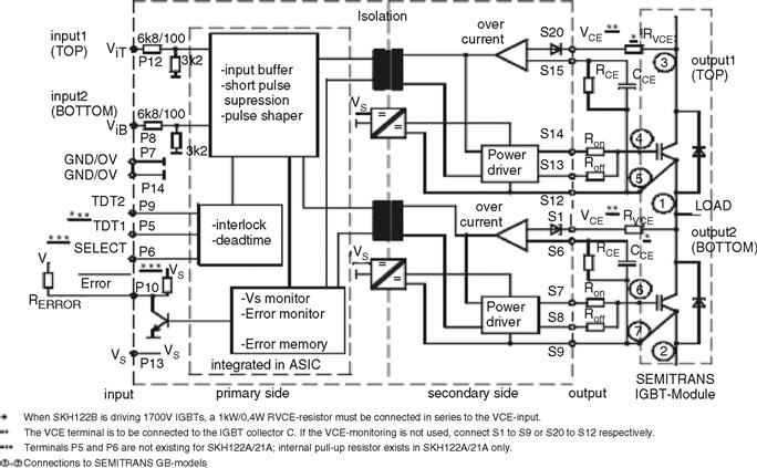
FIGURE 20.22 SKHI22 integrated half-bridge IGBT module capable of operation at 1200 V. A product of the Semikron Corporation.
Each module is configured for a half-bridge inverter configuration and one additional driver module can be added for each inverter leg needed. The modules come in a variety of output current capabilities, depending on the IGBT drive requirements, with usable operating frequencies ranging from the low kHz range up to 30 kHz.
Another manufacturer of isolated gate driver modules is Eupec semiconductor [10]. These modules employ a mono-lithically integrated coreless planar transformer design in a gate driver IC. This allows it to be substantially smaller and cheaper [6]. These modules are operational to 60 kHz with output current capabilities in excess of 2 A peak. The EUPEC EICE-Driver (2ED020I12-F) is shown in Fig. 20.23.
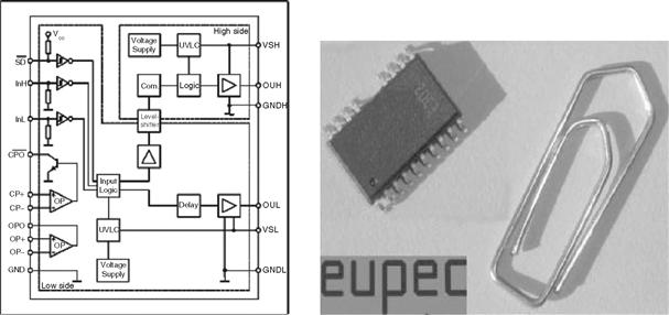
FIGURE 20.23 EUPEC EICE-Driver incorporating monolithic coreless transformer technology allowing for a substantial reduction in the device size.
20.5.2 Non-isolated Electronic Level Shifted Drivers
The International Rectifier Corporation has developed a family of low cost gate driver ICs for the power electronics industry [11]. International Rectifiers, gate driver ICs (Fig. 20.24) utilize electronic level shifting for conveying the switching signal to the high-side switch and a bootstrap technique for the generation of a floating supply. These ICs are relatively inexpensive and are being used mainly in the low cost consumer electronics industry. Application include Electronic Ballasts and low to medium power inverter applications such as variable speed drives and DC to single-phase AC backup inverter systems. Available in a single-channel, half-bridge, or three-phase inverter driver IC, these devices require a minimum amount of external components. Intelligent features like under voltage lockout, shut down, and current sensing inputs are included in the driver IC.
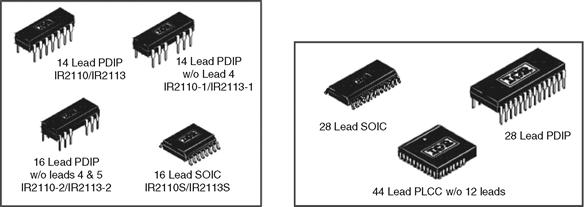
FIGURE 20.24 International Rectifiers IR2113 (Left) and the IR2233 (Right) high voltage gate driver ICs.
Functional diagrams of the IR2113 half-bridge driver and the IR2233 (Three-phase full-bridge) driver are shown in Fig. 20.25. The driver section of the IR2233 comprises a similar structure as the IR2113's bootstrap and level shifting circuitry. Even though the IR range of driver ICs do not provide isolation between the control and driver electronics, this device is a low cost and very compact solution for low to medium power applications where electrical noise and interference can be managed by PCB circuit layout techniques. The IR2113 half-bridge driver is capable of sourcing and sinking 2 A peak current to a capacitive load without external buffer circuitry. This feature coupled with low propagation delay times makes this device capable of operating at frequencies in excess of 100 kHz.
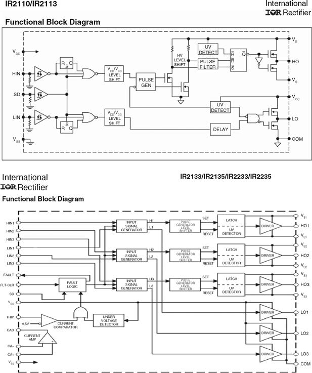
FIGURE 20.25 Functional diagrams of the IR2113 half-bridge driver and the IR2233 three-phase full-bridge driver.
The IR2113 and IR2233 are capable of driving floating loads (high-side switches) at 600 and 1200 V DC bus voltages, respectively, making them suitable for most direct off-line single-phase and three-phase inverter applications.
Other driver ICs available include POWEREX's M57959L and INTERSIL'S HIP2500 bridge driver.
20.5.3 High-speed Gate Drivers
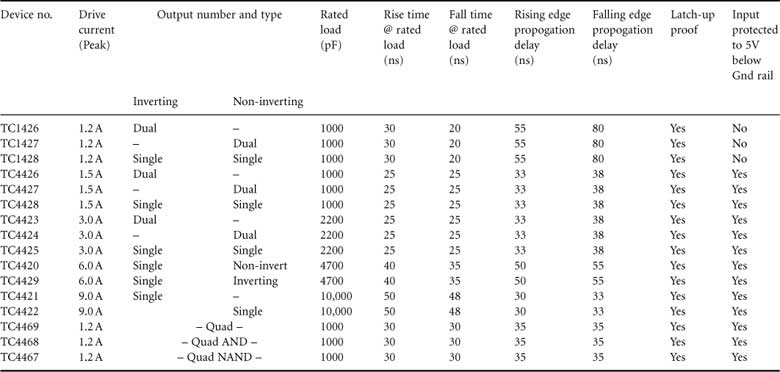
In the quest for high conversion efficiency and high power densities, the trend in power electronics is the move towards high converter switching frequencies at increasingly higher power levels. The main reason for this is to reduce the size of the energy transfer and storage components such as transformers, capacitors, and inductors. This results in a substantial reduction in component size and to a certain extent also cost. Achieving the objectives of high speed and high power switching requires fast switching power semiconductors. These devices are readily available, but as the device die-size increases with voltage and current requirements, so does its gate drive power requirements. This is due to an increase in device input capacitance as the die-size is increased. Low impedance gate driver electronics capable of delivering gate peak drive currents to large die-size IGBTs and power MOS-FETs in excess of 8 A are often required. In order to meet these requirements, driver ICs must be able to deliver these large pulse currents efficiently at high switching frequencies. This is mainly due to a limitation in the maximum allowable device power dissipation. Device package power dissipation is typically limited to around 1.5 W for a DIP-14 IC without heat sinking. Many manufacturers have high speed driver solutions which realize drivers with low output impedances such as the TC4427 and the TC4422. These devices are available as single or dual channel drivers capable of delivering up to 9 A peak to a 1–10 nF capacitive load with a typical rise time of 30–50 ns. A table of available high-speed drivers from TelCom Semiconductor Inc. is shown in Table 20.3 [12].
TABLE 20.3 High current high-speed driver ICs available from TelCom semiconductor
20.5.4 Resonant Gate Drivers
High speed gate driving requires the driver and power semiconductor device impedance to be as low as possible. It is also adversely affected by parasitic inductance and capacitance caused by incorrect layout of the gate driver circuit. Sometimes these unavoidable parasitic elements tend to increase the gate drive loop impedance, (between the driver and the power semiconductor device) resulting in a limitation of the peak current drawn by the device gate. This limits the maximum achievable switching speed of the device. It also results in uncontrolled voltage excursions on the device gate, making high-speed driver circuit design quite challenging.
Resonant gate drivers utilize these parasitic elements in the gate drive loop by virtue of a controlled series resonant mode of operation. The resonant circuit comprises the driver resistance (which is small), the device input capacitance, and its internal gate electrode resistance. By the addition of a defined amount of extra inductance to the gate drive loop, the voltage swing and switching speed of the gate driver can be controlled. A typical resonant gate driver for large die-power semiconductors has been developed by Turboswitchers Inc. A resonant gate driver called the TD-000, employs a patented low loss capacitance driver circuit topology, that reduces the driver power losses to less than half that of conventional high-speed drivers, at all switching frequencies. Operational from a 5 V supply, the driver is capable of high-switching speeds and generates a gate drive voltage swing of up to + 24 to –19 V, depending on the inductance values used. Performance tests show that the TD-000 driver is capable of switching a 500 V/32 A power MOSFET supplied from a 400 V DC bus, in less than 3 ns. This switching speed allows for power electronic converters operating well into the MHz range. Detailed device application information can be found in [13].
20.6 Current and Future Trends
Integrated power electronic solutions have become the current trend for applications with the development of Smart Power modules. These modules contain the entire inverter semiconductor stack as well as fully integrated gate drive circuitry. This technology eliminates the challenges of inverter and gate drive design and allows for fast turnaround times in new product development through rapid prototyping. These devices are available for low to medium power applications and have an operating frequency limit of about 20 kHz.
Power semiconductor device manufacturers are constantly developing better die-structures for their power MOSFETs and IGBTs. This is to reduce device input capacitance, resulting in lower gate drive power requirements at high switching speeds.
20.7 Summary
The aim of this chapter was to expose the reader to the basic concepts, circuits, and technologies for gate drives in power converters. The main focus has been on voltage-controlled devices like power MOSFETs and IGBTs. Once the reader gains a basic understanding of the concepts and available solutions, detailed design information on gate drivers can be found on the device manufacturer's website. This is usually found under technical application notes or technical white papers. Other useful websites for power electronic design forums and application-specific information can be found in [2, 14]. The circuits presented can be adapted for the driving of other devices such as SCRs and power BJTs.
REFERENCES
1. Mohan N, Undeland T, Robbins W. Power Electronics: Converters, Applications and Design. Brisbane: Wiley; 1989.
3. D.R.H. Carter, “Aspects of High Frequency Half-Bridge Circuits”, PhD Thesis, Cambridge University, September 1996.
4. S. Clement, A. Dubhashi, “HV Floating MOS-Gate Driver IC”, Integrated circuit designers manual.
5. Application Note, “Hints and Applications” Design manual, Chapter 3, Semikron Corporation.
6. Munzer M, Ademmer W, Strazalkowski B, Kaschani KT. Coreless Transformer a New Technology for Half Bridge Driver IC’s”. 2005 [application note www.eupec.com].
7. I. de Vries, “High Power and High Frequency Class-DE Inverters”, PhD Thesis, Department of Electrical Engineering, University of Cape Town, August 1999.
8. Application Note AN-937, “Gate Drive Characteristics and Requirements for HEXFET Power MOSFETs”, www.irf.com.
9. Data sheet, SKHI22, www.semikron.com.
10. www.eupec.com.
11. www.irf.com.
12. Application Note 30, “Matching MOSFET drivers to MOSFETs”, TelCom Semiconductor Inc.
13. I. de Vries, “Using Turbodriver-000”, application note, February 2002, www.turboswitchers.com.
14. www.smpstech.com.