
1
Introduction
Department of Electrical and Computer Engineering, University of Illinois, Urbana, Illinois, USA
1.4.1 Single-Switch Circuits
1.5 Tools for Analysis and Design
1.5.1 The Switch Matrix
1.5.2 Implications of Kirchhoff's Voltage and Current Laws
1.5.3 Resolving the Hardware Problem –Semiconductor Devices
1.5.4 Resolving the Software Problem –Switching Functions
1.5.5 Resolving the Interface Problem –Lossless Filter Design
1.7 Summary
1.1 Power Electronics Defined1
It has been said that people do not use electricity, but rather they use communication, light, mechanical work, entertainment, and all the tangible benefits of energy and electronics. In this sense, electrical engineering as a discipline is much involved in energy conversion and information. In the general world of electronics engineering, the circuits engineers design and use are intended to convert information. This is true of both analog and digital circuit design. In radio-frequency applications, energy and information are on more equal footing, but the main function of any circuit is information transfer.
What about the conversion and control of electrical energy itself? Energy is a critical need in every human endeavor. The capabilities and flexibility of modern electronics must be brought to bear to meet the challenges of reliable, efficient energy. It is essential to consider how electronic circuits and systems can be applied to the challenges of energy conversion and management. This is the framework of power electronics, a discipline defined in terms of electrical energy conversion, applications, and electronic devices. More specifically,
DEFINITION Power electronics involves the study of electronic circuits intended to control the flow of electrical energy. These circuits handle power flow at levels much higher than the individual device ratings.
Rectifiers are probably the most familiar examples of circuits that meet this definition. Inverters (a general term for dc–ac converters) and dc–dc converters for power supplies are also common applications. As shown in Fig. 1.1, power electronics represents a median point at which the topics of energy systems, electronics, and control converge and combine [1]. Any useful circuit design for an energy application must address issues of both devices and control, as well as of the energy itself. Among the unique aspects of power electronics are its emphasis on large semiconductor devices, the application of magnetic devices for energy storage, special control methods that must be applied to nonlinear systems, and its fundamental place as a central component of today's energy systems and alternative resources. In any study of electrical engineering, power electronics must be placed on a level with digital, analog, and radio-frequency electronics to reflect the distinctive design methods and unique challenges.
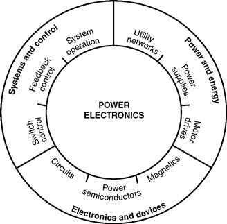
FIGURE 1.1 Control, energy, and power electronics are interrelated.
Applications of power electronics are expanding exponentially. It is not possible to build practical computers, cell phones, personal data devices, cars, airplanes, industrial processes, and a host of other everyday products without power electronics. Alternative energy systems such as wind generators, solar power, fuel cells, and others require power electronics to function. Technology advances such as electric and hybrid vehicles, laptop computers, microwave ovens, flat-panel displays, LED lighting, and hundreds of other innovations were not possible until advances in power electronics enabled their implementation. Although no one can predict the future, it is certain that power electronics will be at the heart of fundamental energy innovations.
The history of power electronics [2–5] has been closely allied with advances in electronic devices that provide the capability to handle high power levels. Since about 1990, devices have become so capable that a transition from a “device-driven” field to an “applications-driven” field continues. This transition has been based on two factors: (1) advanced semiconductors with suitable power ratings exist for almost every application of wide interest, and (2) the general push toward miniaturization is bringing advanced power electronics into a growing variety of products. Although the devices continue to improve, their development now tends to follow innovative applications.
1.2 Key Characteristics
All power electronic circuits manage the flow of electrical energy between an electrical source and a load. The parts in a circuit must direct electrical flows, not impede them. A general power conversion system is shown in Fig. 1.2. The function of the power converter in the middle is to control the energy flow between a source and a load. For our purposes, the power converter will be implemented with a power electronic circuit. Because a power converter appears between a source and a load, any energy used within the converter is lost to the overall system. A crucial point emerges: to build a power converter, we should consider only lossless components. A realistic converter design must approach 100% efficiency.
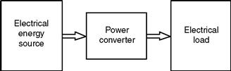
FIGURE 1.2 General system for electric power conversion. (From [2], © 1998, Oxford University Press, Inc.; used by permission.)
A power converter connected between a source and a load also affects system reliability. If the energy source is perfectly reliable (it is available all the time), then a failure in the converter affects the user (the load) just as if the energy source had failed. An unreliable power converter creates an unreliable system. To put this in perspective, consider that a typical American household loses electric power only a few minutes a year. Energy is available 99.999% of the time. A converter must be better than this to prevent system degradation. An ideal converter implementation will not suffer any failures over its application lifetime. Extreme high reliability can be a more difficult objective than high efficiency.
1.2.1 The Efficiency Objective –The Switch
A circuit element as simple as a light switch reminds us that the extreme requirements in power electronics are not especially novel. Ideally, when a switch is on, it has zero voltage drop and will carry any current imposed on it. When a switch is off, it blocks the flow of current regardless of the voltage across it. The device power, the product of the switch voltage and current, is identically zero at all times. A switch therefore controls energy flow with no loss. In addition, reliability is also high. Household light switches perform over decades of use and perhaps 100,000 operations. Unfortunately, a mechanical light switch does not meet all practical needs. A switch in a power supply may function 100,000 times each second. Even the best mechanical switch will not last beyond a few million cycles. Semiconductor switches (without this limitation) are the devices of choice in power converters.
A circuit built from ideal switches will be lossless. As a result, switches are the main components of power converters, and many people equate power electronics with the study of switching power converters. Magnetic transformers and lossless storage elements such as capacitors and inductors are also valid components for use in power converters. The complete concept, shown in Fig. 1.3, illustrates a power electronic system. Such a system consists of an electrical energy source, an electrical load, a power electronic circuit, and a control function.
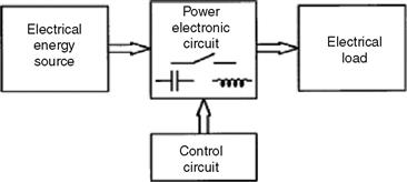
FIGURE 1.3 A basic power electronic system. (From [2], © 1998, Oxford University Press, Inc.; used by permission.)
The power electronic circuit contains switches, lossless energy storage elements, and magnetic transformers. The controls take information from the source, the load, and the designer, and then determine how the switches operate to achieve the desired conversion. The controls are built up with low-power analog and digital electronics.
Switching devices are selected based on their power handling rating –the product of their voltage and current ratings –rather than on power dissipation ratings. This is in contrast to other applications of electronics, in which power dissipation ratings dominate. For instance, a typical stereo receiver performs a conversion from ac line input to audio output. Most audio amplifiers do not use the techniques of power electronics, and the semiconductor devices do not act as switches. A commercial 100-W amplifier is usually designed with transistors big enough to dissipate the full 100W. The semiconductor devices are used primarily to reconstruct the audio information rather than to manipulate the energy flows. The sacrifice in energy is large –a home theater amplifier often functions at less than 10% energy efficiency. In contrast, emerging switching amplifiers do use the techniques of power electronics. They provide dramatic efficiency improvements. A home theater system implemented with switching amplifiers can exceed 90% energy efficiency in a smaller, cooler package. The amplifiers can even be packed inside the loudspeakers.
Switches can reach extreme power levels, far beyond what might be expected for a given size. Consider the following examples.
EXAMPLE 1.1 The NTP30N20 is a metal oxide semiconductor field effect transistor (MOSFET) with a drain current rating of 30 A, a maximum drain source breakdown voltage of 200V, and a rated power dissipation of up to 200 W under ideal conditions. Without a heat sink, however, the device can handle less than 2.5 W of dissipation. For power electronics purposes, the power handling rating is 30 A × 200 V = 6kW. Several manufacturers have developed controllers for domestic refrigerators, air conditioners, and high-end machine tools based on this and similar devices. The second part of the definition of power electronics in Section 1.1 points out that the circuits handle power at levels much higher than that of the ratings of individual devices. Here a device is used to handle 6000 W –compared with its individual rating of no more than 200 W. The ratio 30:1 is high, but not unusual in power electronics contexts. In contrast, the same ratio in a conventional audio amplifier is close to unity.
EXAMPLE 1.2 The IRGPS60B120KD is an insulated gate bipolar transistor (IGBT) –a relative of the bipolar transistor that has been developed specifically for power electronics –rated for 1200 V and 120 A. Its power handling rating is 144kW which is sufficient to control an electric or hybrid car.
1.2.2 The Reliability Objective –Simplicity and Integration
High-power applications lead to interesting issues. In an inverter, the semiconductors often manipulate 30 times their power dissipation capability or more, which implies that only about 3% of the power being controlled is lost. A small design error, unexpected thermal problem, or minor change in layout could alter this somewhat. For instance, if the loss turns out to be 4% rather than 3%, the device stresses are 33% higher, and quick failure is likely to occur. The first issue for reliability in power electronic circuits is that of managing device voltage, current, and power dissipation levels to keep them well within rating limits. This is challenging when power-handling levels are high.
The second issue for reliability is simplicity. It is well established in electronics design that the more parts there are in a system, the more likely it is to fail. Power electronic circuits tend to have few parts, especially in the main energy flow paths. Necessary operations must be carried out through shrewd use of these parts. Often, this means that sophisticated control strategies are applied to seemingly simple conversion circuits.
The third issue for reliability is integration. One way to avoid the reliability-complexity tradeoff is to integrate multiple components and functions on a single substrate. A microprocessor, for example, might contain millions of gates. All interconnections and signals flow within a single chip, and the reliability is near that of a single part. An important parallel trend in power electronic devices involves the integrated module [6]. Manufacturers seek ways to package multiple switching devices, with their interconnections and protection components, together as a unit. Control circuits for converters are also integrated as much as possible to keep the reliability high. The package itself is a factor in reliability, and one that is a subject of active research. Many semiconductor packages include small bonding wires that can be susceptible to thermal or vibration damage. The small geometries also tend to enhance electromagnetic interference among the internal circuit components.
1.3 Trends in Power Supplies
Two distinct trends drive electronic power supplies, one of the major classes of power electronic circuits. At the high end, microprocessors, memory chips, and other advanced digital circuits require increasing power levels and increasing performance at very low voltage. It is a challenge to deliver 100 A or more efficiently at voltages that can be less than 1V. These types of power supplies are expected to deliver precise voltages, even though the load can change by an order of magnitude in nanoseconds.
At the other end is the explosive growth of portable devices with rechargeable batteries. The power supplies for these devices and for other consumer products must be cheap and efficient. Losses in low-cost power supplies are a problem today; often, low-end power supplies and battery chargers draw energy even when their load is off. It is increasingly important to use the best possible power electronics design techniques for these supplies to save energy while minimizing costs. Efficiency standards such as the EnergyStar program place increasingly stringent requirements on a wide range of low-end power supplies.
In the past, bulky “linear” power supplies were designed with transformers and rectifiers from the ac line frequency to provide dc voltages for electronic circuits. In the late 1960s, use of dc sources in aerospace applications led to the development of power electronic dc–dc conversion circuits for power supplies. In a well-designed power electronics arrangement today, called a switch-mode power supply, an ac source from a wall outlet is rectified without direct transformation. The resulting high dc voltage is converted through a dc–dc converter to the 1, 3, 5, and 12 V, or other levels required. A personal computer commonly requires multiple 3.3- and 5-V supplies, 12-V supplies, additional levels, and a separate converter for 1-V delivery to the microprocessor. This does not include supplies for the video display or peripheral devices. Only a switch-mode supply can support such complex requirements with acceptable costs.
Switch-mode supplies often take advantage of MOSFET semiconductor technology. Trends toward high reliability, low cost, and miniaturization have reached the point where a 5-V power supply sold today might last more than 1,000,000 h (more than a century), provide 100 W of output in a package with volume less than 15 cm3, and sell for a price less than US$ 0.10/W. This type of supply brings an interesting dilemma: the ac line cord to plug it in takes up more space than the power supply itself. Innovative concepts such as integrating a power supply within a connection cable will be used in the future.
Device technology for power supplies is also being driven by expanding needs in the automotive and telecommunications industries as well as in markets for portable equipment. The automotive industry is making a transition to higher voltages to handle increasing electric power needs. Power conversion for this industry must be cost effective, yet rugged enough to survive the high vibration and wide temperature range to which a passenger car is exposed. Global communication is possible only when sophisticated equipment can be used almost anywhere. This brings with it a special challenge, because electrical supplies are neither reliable nor consistent throughout much of the world. Although voltage swings in the domestic ac supply in North America are often ± 5% around a nominal value, in many developing nations the swing can be ± 25% −when power is available. Power converters for communications equipment must tolerate these swings and must also be able to make use of a wide range of possible backup sources. Given the enormous size of worldwide markets for mobile devices and consumer electronics, there is a clear need for flexible-source equipment. Designers are challenged to obtain maximum performance from small batteries and to create equipment with minimal energy requirements.
1.4 Conversion Examples
1.4.1 Single-Switch Circuits
Electrical energy sources take the form of dc voltage sources at various values, sinusoidal ac sources, polyphase sources, among others. A power electronic circuit might be asked to transfer energy between two different dc voltage levels, between an ac source and a dc load, or between sources at different frequencies. It might be used to adjust an output voltage or power level, drive a nonlinear load, or control a load current. In this section, a few basic converter arrangements are introduced, and energy conservation provides a tool for analysis.
EXAMPLE 1.3 Consider the circuit shown in Fig. 1.4. It contains an ac source, a switch, and a resistive load. It is a simple but complete power electronic system.
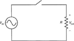
FIGURE 1.4 A simple power electronic system.(From [2], © 1998, Oxford University Press, Inc.; used by permission.)
Let us assign a (somewhat arbitrary) control scheme to the switch. What if the switch is turned on whenever Vac > 0, and turned off otherwise? The input and output voltage waveforms are shown in Fig. 1.5. The input has a time average of 0, and root-mean-square (RMS) value equal to Vpeak √2, where Vpeak is the maximum value of Vac. The output has a nonzero average value given by
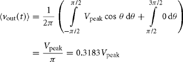 (1.1)
(1.1)
and an RMS value equal to Vpeak/2. Since the output has nonzero dc voltage content, the circuit can be used as an ac–dc converter. To make it more useful, a low-pass filter would be added between the output and the load to smooth out the ac portion. This filter needs to be lossless, and will be constructed from only inductors and capacitors.
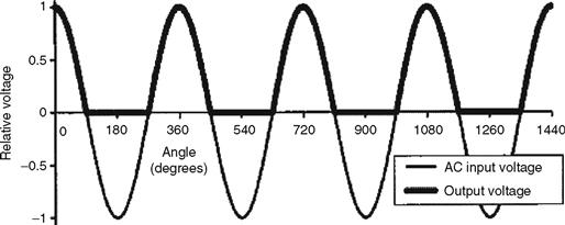
FIGURE 1.5 Input and output waveforms for Example 1.4.
The circuit in Example 1.3 acts as a half-wave rectifier with a resistive load. With the hypothesized switch action, a diode can substitute for the ideal switch. The example confirms that a simple switching circuit can perform power conversion functions. But note that a diode is not, in general, the same as an ideal switch. A diode places restrictions on the current direction, whereas a true switch would not. An ideal switch allows control over whether it is on or off, whereas a diode's operation is constrained by circuit variables.
Consider a second half-wave circuit, now with a series L–R load, shown in Fig. 1.6.
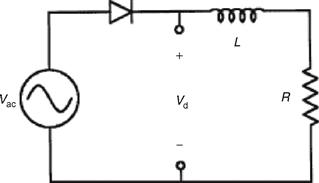
FIGURE 1.6 Half-wave rectifier with L–R load for Example 1.5.
EXAMPLE 1.4 A series diode L–R circuit has ac voltage source input. This circuit operates much differently than the half-wave rectifier with resistive load. A diode will be on if forward-biased, and off if reverse-biased. In this circuit, when the diode is off, the current will be zero.
Whenever the diode is on, the circuit is the ac source with L–R load. Let the ac voltage be V0 cos(ωt). From Kirchhoff's Voltage Law (KVL),
![]()
Let us assume that the diode is initially off (this assumption is arbitrary, and we will check it as the example is solved). If the diode is off, the diode current is i=0, and the voltage across the diode will be vac. The diode will become forward-biased when vac becomes positive. The diode will turn on when the input voltage makes a zero-crossing in the positive direction. This allows us to establish initial conditions for the circuit: i(t0) = 0, t0 = −ϕ/(2ω). The differential equation can be solved in a conventional way to give
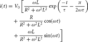 (1.2)
(1.2)
where τ is the time constant L/R. What about when the diode is turned off? The first guess might be that the diode turns off when the voltage becomes negative, which is not correct. From the solution, we can note that the current is not zero when the voltage first becomes negative. If the switch attempts to turn off, it must instantly drop the inductor current to zero. The derivative of current in the inductor, di/dt, would become negative infinite. The inductor voltage L(di/dt) similarly becomes negative infinite, and the devices are destroyed. What really happens is that the falling current allows the inductor to maintain forward bias on the diode. The diode will turn off only when the current reaches zero. A diode has definite properties that determine the circuit action, and both the voltage and current are relevant. Figure 1.7 shows the input and output waveforms for a time constant τ equal to about one-third of the ac waveform period.
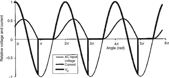
FIGURE 1.7 Input and output waveforms for Example 1.5.
1.4.2 The Method of Energy Balance
Any circuit must satisfy conservation of energy. In a lossless power electronic circuit, energy is delivered from source to load, possibly through an intermediate storage step. The energy flow must balance over time such that the energy drawn from the source matches that delivered to the load. The converter in Fig. 1.8 serves as an example of how the method of energy balance can be used to analyze circuit operation.
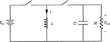
FIGURE 1.8 Energy transfer switching circuit for Example 1.5.(From [2], (c) 1998, Oxford University Press, Inc.; used by permission.)
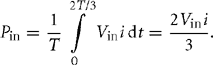
EXAMPLE 1.5 The switches in the circuit of Fig. 1.8 are controlled cyclically to operate in alternation: when the left switch is on, the right switch is off, and so on. What does the circuit do if each switch operates half the time? The inductor and capacitor have large values.
When the left switch is on, the source voltage Vin appears across the inductor. When the right switch is on, the output voltage Vout appears across the inductor. If this circuit is to be viewed as a useful converter, the inductor should receive energy from the source and then deliver it to the load without loss. Over time, this means that energy does not build up in the inductor, but instead flows through on average. The power into the inductor, therefore, must equal the power out, at least over a cycle. Therefore, the average power in must equal the average power out of the inductor. Let us denote the inductor current as i. The input is a constant voltage source. Because L is large, this constant voltage source will not be able to change the inductor current quickly, and we can assume that the inductor current is also constant. The average power into L over the cycle period T is
 (1.3)
(1.3)
For the average power out of L, we must be careful about current directions. The current out of the inductor will have a value −i. The average output power is
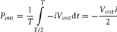 (1.4)
(1.4)
For this circuit to be viewed useful as a converter, the net energy should flow from the source to the load over time. The power conservation relationship Pin = Pout requires that Vout = –Vin.
The method of energy balance shows that, when operated as described in the example, the circuit shown in Fig. 1.8 serves as a polarity reverser. The output voltage magnitude is the same as that of the input, but the output polarity is negative with respect to the reference node. The circuit is often used to generate a negative supply for analog circuits from a single positive input level. Other output voltage magnitudes can be achieved at the output if the switches alternate at unequal times.
If the inductor in the polarity reversal circuit is moved instead to the input, a step-up function is obtained. Consider the circuit shown in Fig. 1.9 in the following example.
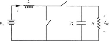
FIGURE 1.9 Switching converter Example 1.6.(From [2], © 1998, Oxford University Press, Inc.; used by permission.)
EXAMPLE 1.6 The switches shown in Fig. 1.9 are controlled cyclically in alternation. The left switch is on for two-thirds of each cycle, and the right switch for the remaining one-third of each cycle. Determine the relationship between Vin and Vout. The inductor's energy should not build up when the circuit is operating normally as a converter. A power balance calculation can be used to relate the input and output voltages. Again, let i be the inductor current. When the left switch is on, power is injected into the inductor. Its average value is
 (1.5)
(1.5)
Power leaves the inductor when the right switch is on. Care must be taken with respect to polarities, and the current should be set negative to represent output power.
The result is
(1.6)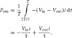
When the input and output power are equated,
![]() (1.7)
(1.7)
and the output voltage is found to be triple the input. Many seasoned engineers find the dc–dc step-up function shown in Fig. 1.9 to be surprising. Yet, it is just one example of such action. Others (including flyback circuits related to Fig. 1.8) are used in systems ranging from controlled power supplies to spark ignitions for automobiles.
The circuits in the preceding examples have few components, provide useful conversion functions, and are efficient. If the switching devices are ideal, each circuit is lossless. Over the history of power electronics, development has tended to flow around the discovery of such circuits: a circuit with a particular conversion function is discovered, analyzed, and applied. As the circuit moves from laboratory testing to a complete commercial product, control and protection functions are added. The power portion of the circuit remains close to the original idea. The natural question arises as to whether a systematic approach to conversion is possible: can we start with a desired function and design an appropriate converter, rather than starting from the converter and working backwards toward the application? What underlying principles can be applied to design and analysis? In this chapter, a few of the key concepts are introduced. Note that, although many of the circuits look deceptively simple, all circuits are nonlinear systems with unusual behavior.
1.5 Tools for Analysis and Design
1.5.1 The Switch Matrix
The most readily apparent difference between a power electronic circuit and other types of electronic circuits is the switch action. In contrast to a digital circuit, the switches do not indicate a logic level. Control is effected by determining the times at which switches should operate. Whether there is just one switch or a large group, there is a complexity limit: if a converter has m inputs and n outputs, even the densest possible collection of switches would have a single switch between each input and output lines. The m × n switches in the circuit can be arranged according to their connections. The pattern suggests a matrix, as shown in Fig. 1.10.
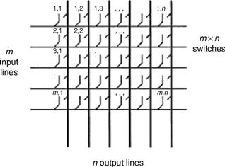
FIGURE 1.10 The general switch matrix.
Power electronic circuits fall into two broad classes:
1. Direct switch matrix circuits. In these circuits, energy storage elements are connected to the matrix only at the input and output terminals. The storage elements effectively become part of the source or the load. A rectifier with an external low-pass filter is an example of a direct switch matrix circuit. In the literature, ac–ac versions of these circuits are sometimes called matrix converters.
2. Indirect switch matrix circuits, also termed embedded converters. These circuits, like the polarity-reverser example, have energy storage elements connected within the matrix structure. Indirect switch matrix circuits are most commonly analyzed as a cascade connection of direct switch matrix circuits with storage in between.
The switch matrices in realistic applications are small. A 2 × 2 switch matrix, for example, covers all possible cases with a single-port input source and a two-terminal load. The matrix is commonly drawn as the H-bridge shown in Fig. 1.11. A more complicated example is the three-phase bridge rectifier shown in Fig. 1.12. There are three possible inputs, and the two terminals of the dc circuit provide outputs, which gives a 3 × 2 switch matrix. In a computer power supply with five separate dc loads, the switch matrix could be 2 × 10. Very few practical converters have more than 24 switches, and most designs use fewer than 12.
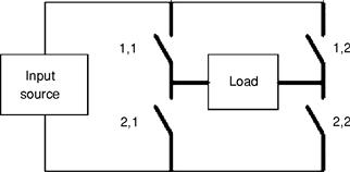
FIGURE 1.11 H-bridge configuration of a 2× 2 switch matrix.
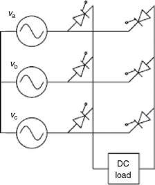
FIGURE 1.12 Three-phase bridge rectifier circuit, a 3 × 2 switch matrix.
A switch matrix provides a way to organize devices for a given application. It also helps us focus on three major task areas, which must be addressed individually and effectively in order to produce a useful power electronic system.
• The “Hardware” Task –Build a switch matrix. This involves the selection of appropriate semiconductor switches and the auxiliary elements that drive and protect them.
• The “Software” Task –Operate the matrix to achieve the desired conversion. All operational decisions are implemented by adjusting switch timing.
• The “Interface” Task –Add energy storage elements to provide the filters or intermediate storage necessary to meet the application requirements. Lossless filters with simple structures are required.
In a rectifier or other converter, we must choose the electronic parts, how to operate them, and how best to filter the output to satisfy the needs of the load.
1.5.2 Implications of Kirchhoff's Voltage and Current Laws
A major challenge of switch circuits is their capacity to “violate” circuit laws. First, consider the simple circuits shown in Fig. 1.13. We might try the circuit shown in Fig. 1.13a for ac-dc conversion, but there is a problem. According to Kirchhoff's Voltage Law (KVL), the “sum of voltage drops around a closed loop is zero.” However, with the switch closed, the sum of voltages around the loop is not zero. In reality, this is not a valid result. Instead, a very large current will flow and cause a large I · R drop in the wires. KVL will be satisfied by the wire voltage drop, but a fire or, better yet, fuse action, might result. There is, however, nothing that would prevent an operator from trying to close the switch. KVL, then, implies a crucial restriction: a switch matrix must not attempt to interconnect unequal voltage sources directly. Notice that a wire, or dead short, can be thought of as a voltage source with V = 0, so KVL is a generalization of avoiding shorts across an individual voltage source.
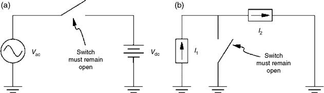
FIGURE 1.13 Hypothetical power converters: (a) possible ac-dc converter (b) possible dc–dc converter.(From [2], © 1998, Oxford University Press Inc.; used by permission.)
A similar constraint holds for Kirchhoff's Current Law (KCL) that states that “currents into a node must sum to zero.” When current sources are present in a converter, we must avoid any attempts to violate KCL. In Fig. 1.13b, if the current sources are different and if the switch is opened, the sum of the currents into the node will not be zero. In a real circuit, high voltages will build up and cause an arc to create another current path. This situation has real potential for damage, and a fuse will not help. As a result, KCL implies the restriction that a switch matrix must not attempt to interconnect unequal current sources directly. An open circuit can be thought of as a current source with I = 0, so KCL applies to the problem of opening an individual current source.
In contrast to conventional circuits, in which KVL and KCL are automatically satisfied, switches do not “know” KVL or KCL. If a designer forgets to check, and accidentally shorts two voltages or breaks a current source connection, some problem or damage will result. KVL and KCL place necessary constraints on the operation of a switch matrix. In the case of voltage sources, switches must not act to create short-circuit paths among unlike sources. In the case of KCL, switches must act to provide a path for currents. These constraints drastically reduce the number of valid switch-operating conditions in a switch matrix, thereby leading to manageable operating design problems.
When energy storage is included, there are interesting implications of the circuit law restrictions. Figure 1.14 shows two “circuit law problems.” In Fig. 1.14a, the voltage source will cause the inductor current to ramp up indefinitely, since V = L di/dt. We might consider this to be a “KVL problem” because the long-term effect is similar to shorting the source. In Fig. 1.14b, the current source will cause the capacitor voltage to ramp toward infinity. This causes a “KCL problem”; eventually, an arc will be formed to create an additional current path, just as if the current source had been opened. Of course, these connections are not problematic if they are only temporary. However, it should be evident that an inductor will not support dc voltage, and a capacitor will not support dc current. On average, over an extended time interval, the voltage across an inductor must be zero, and the current into a capacitor must be zero.
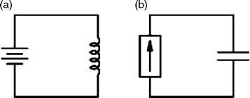
FIGURE 1.14 Short-term KVL and KCL problems in energy storage circuits: (a) an inductor cannot sustain dc voltage indefinitely; (b) a capacitor cannot sustain dc current indefinitely.
1.5.3 Resolving the Hardware Problem –Semiconductor Devices
A switch is either on or off. When on, an ideal switch will carry any current in any direction. When off, it will never carry current, no matter what voltage is applied. It is entirely lossless and changes from its on-state to its off-state instantaneously. A real switch can only approximate an ideal switch. The following are the aspects of real switches that differ from the ideal:
• limits on the amount and direction of on-state current;
• a nonzero on-state voltage drop (such as a diode forward voltage);
• some levels of leakage current when the device is supposed to be off;
• limitations on the voltage that can be applied when off;
• operating speed. The duration of transition between the on-states and off-states is important.
The degree to which the properties of an ideal switch must be met by a real switch depends on the application. For example, a diode can easily be used to conduct dc current; the fact that it conducts only in one direction is often an advantage, not a weakness.
Many different types of semiconductors have been applied in power electronics. In general, these fall into three groups:
1. Diodes, which are used in rectifiers, dc–dc converters, and in supporting roles.
2. Transistors, which in general are suitable for control of single-polarity circuits. Several types of transistors are applied to power converters. The IGBT type is unique to power electronics and has good characteristics for applications such as inverters.
3. Thyristors, which are multijunction semiconductor devices with latching behavior. In general, thyristors can be switched with short pulses and then maintain their state until current is removed. They act only as switches. The characteristics are especially well suited to high-power controllable rectifiers, they have been applied to all power-conversion applications.
Some of the features of the most common power semiconductors are listed in Table 1.1. The table shows a wide variety of speeds and rating levels. As a rule, faster speeds apply to lower ratings. For each device type, cost tends to increase both for faster devices and for devices with higher power-handling capacity.
TABLE 1.1 Examples of semiconductor devices used in power electronics
| Device type | Characteristics of power devices |
| Diode | Current ratings from under 1 A to more than 5000 A. Voltage ratings from 10 V to 10 kV or more. The fastest power devices switch in less than 10 ns, whereas the slowest require 100 μ s or more. The function of a diode applies in rectifiers and dc–dc circuits. |
| BJT | (Bipolar junction transistor) Conducts collector current (in one direction) when sufficient base current is applied. The function applies to dc–dc circuits. Power BJTs have mostly been supplanted by FETs and IGBTs. |
| FET | (Field effect transistor) Conducts drain current when sufficient gate voltage is applied. Power FETs (nearly always enhancement-mode MOSFETs) have a parallel connected reverse diode by virtue of their construction. Ratings from about 0.5 A to about 150 A and 20 V up to 1200 V. Switching times are fast, from 20 ns or less up to 200 ns. The function applies to dc–dc conversion, where the FET is in wide use, and to inverters. |
| IGBT | (Insulated gate bipolar transistor) A special type of transistor that has the function of a BJT with its base driven by an FET. Faster than a BJT of similar ratings, and easy to use. Ratings from 10 A to more than 600 A, with voltages of 600 to 2500 V. The IGBT is popular in inverters from about 1 to 200 kW or more. It is found almost exclusively in power electronics applications. |
| SCR | (Silicon-controlled rectifier) A thyristor that conducts like a diode after a gate pulse is applied. Turns off only when current becomes zero. Prevents current flow until a pulse appears. Ratings from 10 A up to more than 5000 A, and from 200 V up to 6 kV. Switching requires 1 to 200 μ s. Widely used for controlled rectifiers. The SCR is found almost exclusively in power electronics applications, and is the most common member of the thyristor family. |
| GTO | (Gate turn-off thyristor) An SCR that can be turned off by sending a negative pulse to its gate terminal. Can substitute for transistors in applications above 200 kW or more. The ratings approach those of SCRs, and the speeds are similar as well. |
| TRIAC | A semiconductor constructed to resemble two SCRs connected in reverse parallel. Ratings from 2 to 50 A and 200 to 800 V. Used in lamp dimmers, home appliances, and hand tools. Not as rugged as many other device types, but very convenient for many ac applications. |
| IGCT | (Integrated gate commutated thyristor) A combination device that includes a high-power thyristor and external electronics to control it. This device is a member of a larger family of combination devices, in which multiple semiconductor chips packaged together perform a single power function. The IGCT provides a high-performance GTO function for power levels above 1 MW or more. |
Conducting direction and blocking behavior are fundamentally tied to the device type, and these basic characteristics constrain the choice of device for a given conversion function. Consider again a diode. It carries current in only one direction and always blocks current in the other direction. Ideally, the diode exhibits no forward voltage drop or off-state leakage current. Although an ideal diode lacks the many features of an ideal switch, it is an important switching device. Other real devices operate with polarity limits on current and voltage and have corresponding ideal counterparts. It is convenient to define a special type of switch to represent this behavior: the restricted switch.
DEFINITION A restricted switch is an ideal switch with the addition of restrictions on the direction of current flow and voltage polarity. The ideal diode is one example of a restricted switch.
The diode always permits current flow in one direction, while blocking flow in the other direction. It therefore represents a forward-conducting reverse-blocking restricted switch and operates in one quadrant on a graph of device current versus. voltage. This function is automatic –the two diode terminals provide all the necessary information for switch action. Other restricted switches require a third gate terminal to determine their state. Consider the polarity possibilities given in Table 1.2. Additional functions such as bidirectional-conducting reverse-blocking can be obtained by reverse connection of one of the five types in the table.
TABLE 1.2 The types of restricted switches
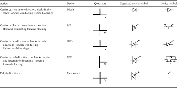
The quadrant operation shown in the table indicates polarities. For example, the current in a diode will be positive when on, and the voltage will be negative when off. This means diode operation is restricted to the single quadrant comprising the upper vertical (current) axis and the left horizontal (voltage) axis. Other combinations appear in the table. Symbols for restricted switches can be built up by interpreting the diode's triangle as the current-carrying direction and the bar as the blocking direction. Five types of symbols can be drawn as shown in Table 1.2. These symbols are used infrequently, but are useful for showing the polarity behavior of switching devices. A circuit drawn with restricted switches represents an idealized power converter.
Restricted switch concepts guide the selection of devices. For example, consider an inverter intended to deliver ac load current from a dc voltage source. A switch matrix built to perform this function must be able to manipulate ac current and dc voltage. Regardless of the physical arrangement of the matrix, we would expect bidirectional-conducting forward-blocking switches to be useful for this conversion. This is a correct result: modern inverters operating from dc voltage sources are built with FETs or with IGBTs packaged with reverse-parallel diodes. As new power devices are introduced to the market, it is straightforward to determine what types of converters will use them.
1.5.4 Resolving the Software Problem –Switching Functions
The physical m × n switch matrix can be associated with a mathematical m × n switch state matrix. Each element of this matrix, called a switching function, shows whether the corresponding physical device is on or off.
DEFINITION A switching function, q(t), has a value of 1 when the corresponding physical switch is on and 0 when it is off. Switching functions are discrete-valued functions of time, and control of switching devices can be represented with them.
Figure 1.15 shows a typical switching function. It is periodic, with period T, representing the most likely repetitive switch action in a power converter. For convenience, it is drawn on a relative time scale that begins at 0 and draws out the square wave period by period. The actual timing is arbitrary, so the center of the first pulse is defined as a specified time t0 in the figure. In many converters, the switching function is generated as an actual control voltage signal that might drive the gate of either a MOSFET or some other semiconductor switching device.
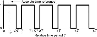
FIGURE 1.15 A generic switching function with period T, duty ratio D, and time reference t0.
The timing of switch action is the only alternative for control of a power converter. Because switch action can be represented with a discrete-valued switching function, timing can be represented within the switching function framework. On the basis of Fig. 1.15, a generic switching function can be characterized completely with three parameters:
1. The duty ratio, D, is the fraction of time during which the switch is on. For control purposes, the on-time interval or pulse width can be adjusted to achieve a desired result. We can term this adjustment process pulse-width modulation (PWM), perhaps the most important process for implementing control in power converters.
2. The frequency fswitch = 1/T (with radian frequency ω = 2πfswitch) is most often constant, although not in all applications. For control purposes, frequency can be adjusted. This strategy is sometimes used in low-power dc–dc converters to manage wide load ranges. In other converters, frequency control is unusual because the operating frequency is often dictated by the application.
3. The time delay t0 or phase ϕ0 =ωt0. Rectifiers often use phase control to provide a range of adjustment. Phase-shifted bridge circuits are common for high-power dc–dc conversion. A few specialized ac–ac converter applications use phase modulation.
With just three parameters to vary, there are relatively few possible ways to control any power electronic circuit. dc–dc converters and inverters usually rely on duty ratio adjustment (PWM) to alter their behavior. Phase control is common in controlled rectifier applications.
Switching functions are powerful tools for the general representation of converter action [7]. The most widely used control approaches derive from averages of switching functions [2,8]. Their utility comes from their application in writing circuit equations. For example, in the boost converter shown in Fig. 1.9, the loop and node equations change depending on which switch is acting at a given moment. The two possible circuit configurations each have distinct equations. Switching functions allow them to be combined. By assigning switching functions q1(t) and q2(t) to the left- and right-switching devices, respectively, we obtain
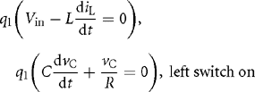 (1.8)
(1.8)
 (1.9)
(1.9)
Because the switches alternate, and the switching functions must be 0 or 1, these sets of equations can be combined to give
![]() (1.10)
(1.10)
The combined expressions are simpler and easier to analyze than the original equations.
For control purposes, the average of equations such as (1.10) often proceeds with the replacement of switching functions q with duty ratios d. The discrete time action of a switching function thus will be represented by an average duty ratio parameter. Switching functions, the advantages gained by averaging, and control approaches such as PWM are discussed at length in several chapters in this handbook.
1.5.5 Resolving the Interface Problem –Lossless Filter Design
Lossless filters for power electronic applications are sometimes called smoothing filters [9]. In applications in which dc outputs are of interest, such filters are commonly implemented as simple low-pass LC structures. The analysis is facilitated because in most cases the residual output waveform, termed ripple, has a predictable shape. Filter design for rectifiers or dc–dc converters is a question of choosing storage elements large enough to keep ripple low, but not so large that the whole circuit becomes unwieldy or expensive.
Filter design is more challenging when ac outputs are desired. In some cases, this is again an issue of low-pass filter design. However, in many applications, low-pass filters are not adequate to meet low noise requirements. In these situations, active filters can be used. In power electronics, the term active filter refers to lossless switching converters that actively inject or remove energy moment-by-moment to compensate for distortion. The circuits (discussed in Chapter 41 –Active Filters in this handbook) are not related to the linear active filter op-amp circuits used in analog signal processing. In ac applications, there is a continuing opportunity for innovation in filter design.
1.6 Sample Applications
Although power electronics is becoming universal for electronic systems, a few emerging applications have generated wide interest. Some are discussed briefly here to introduce the breadth of activity in the field.
A hybrid electric vehicle typically has two major power electronic systems and dozens or even hundreds of smaller systems [10]. The two large units are the inverter system, which controls the electric drive motor, and a rectifier system, which manages battery charging. Smaller systems include motor controllers in electric power steering units, lighting electronics for high-intensity headlamps, controllers for the wide range of small motors that actuate everything from windshield wipers to DVD players, and power supplies for the host of microcontrollers embedded in a modern car. As plug-in hybrid and electric cars continue to develop, the efficiency and sophistication of battery chargers and drive motor controllers will increase.
In a hybrid car, a typical inverter rating is about 50 kW. Fully electric automobiles have inverter ratings to about 200 kW. Hybrid and electric drive power levels increase from there to include multimegawatt inverters that power high-speed trains.
At the other power extreme, designers have been working on small power electronic systems that extract energy from various ambient sources for local purposes [11]. These energy harvesting applications will be an emerging growth area. An example application is a corrosion sensor, built into a highway bridge, that gathers energy from vibration. The vibration energy is converted and stored, then used for intermittent communication with a central monitoring computer. Typical power levels can be less than 0.001 W.
Solar, wind, and other alternative energy resources are tightly linked to power electronics. A typical solar panel produces about 30-V dc, with tolerances from 20 to 40 V or more. This randomly changing dc source must be converted to clean, tightly regulated ac voltage that synchronizes to the electricity grid and delivers energy. Solar inverter efficiency, reliability, and cost are major factors in successful energy innovation. A dual application, meaning that energy flows in the opposite direction but that many other characteristics are shared, is that of solid-state lighting [12]. In that case, flexible control of a dc current must be provided from an ac grid source.
For wind energy, a typical large-scale wind turbine can produce 2 MW of high-frequency ac power. The frequency and voltage vary rapidly according to wind speed. This power must be converted to fixed frequency and voltage for grid interconnection.
1.7 Summary
Power electronics is the study of electronic circuits for the control and conversion of electrical energy. The technology is a critical part of our energy infrastructure and is central for a wide range of uses of electricity. For power electronics design, we consider only those circuits and devices that, in principle, introduce no loss and achieve near-perfect reliability. The two key characteristics of high efficiency and high reliability are implemented with switching circuits, supplemented with energy storage. Switching circuits can be organized as switch matrices. This facilitates their analysis and design.
In a power electronic system, the three primary challenges are the hardware problem of implementing a switch matrix, the software problem of deciding how to operate that matrix, and the interface problem of removing unwanted distortion and providing the user with the desired clean power source. The hardware is implemented with a few special types of power semiconductors. These include several types of transistors, especially MOSFETs and IGBTs, and several types of thyristors, especially SCRs and GTOs. The software problem can be represented in terms of switching functions. The frequency, duty ratio, and phase of switching functions are available for operational purposes. The interface problem is addressed by means of lossless filter circuits. Most often, these are lossless LC passive filters to smooth out ripple or reduce harmonics. Active filter circuits also have been applied to make dynamic corrections in power conversion waveforms.
Improvements in devices and advances in control concepts have led to steady improvements in power electronic circuits and systems. This is driving tremendous expansion of applications. Personal computers, for example, would be unwieldy and inefficient without power electronic dc supplies. Mobile devices and laptop computers would be impractical. High-efficiency lighting, motor controls, and a wide range of industrial controls depend on power electronics. Strong growth is occurring in automotive applications, in lighting, in dc power supplies for portable devices, in high-end converters for advanced microprocessors, and in alternative and renewable energy. During the next generation, we will reach a time when almost all electrical energy is processed through power electronics somewhere in the path from generation to end use.
References
1. Motto J, ed. Introduction to Solid State Power Electronics. Youngwood, PA: Westinghouse; 1977.
2. Krein PT. Elements of Power Electronics. New York: Oxford University Press; 1998.
3. Jahns TM, Owen EL. Ac adjustable-speed drives at the millennium: How did we get here?. In: Proc. IEEE Applied Power Electronics Conf.. 2000. [pp. 18–26].
4. Herskind CC, McMurray W. History of the static power converter committee. IEEE Trans. Industry Applications. July 1984; vol. IA-20(no. 4):1069–1072.
5. Owen EL. Origins of the inverter. IEEE Industry Applications Mag.. January 1996; vol. 2:64.
6. Van Wyk JD, Lee FC. Power electronics technology at the dawn of the new millennium –status and future. In: Rec., IEEE Power Electronics Specialists Conf.. 1999. [pp. 3–12].
7. Wood P. Switching Power Converters. New York: Van Nostrand Reinhold; 1981.
8. Erickson R. Fundamentals of Power Electronics. New York: Chapman and Hall; 1997.
9. Krein PT, Hamill DC. Smoothing circuits. In: Webster J, ed. Wiley Encyclopedia of Electrical and Electronics Engineering. New York: John Wiley; 1999.
10. Emadi A, Rajashekara K, Williamson SS, Lukic SM. Topological overview of hybrid electric and fuel cell vehicular power system architectures and configurations. IEEE Trans. Vehicular Tech.. 2005; vol. 54 [pp. 763–770].
11. Sazonov E, Haodong L, Curry D, Pillay P. Self-powered sensors for monitoring of highway bridges. IEEE Sensors Journal. 2009; vol. 9 [pp. 1422–1429].
12. Loo KH, Lun W-K, Tan S-C, Lai YM, Tse CK. On driving techniques for LEDs: toward a generalized methodology. IEEE Trans. Power Electronics. December 2009; vol. 24 [pp. 2967–2976].
1 Portions of this chapter are taken from P. T. Krein, Elements of Power Electronics. New York: Oxford University Press, 1998. © 1998, Oxford University Press. Used by permission.