
2
The Power Diode
School of EEE Nanyang Technological University, Nanyang Avenue, Singapore
2.4.1 Voltage Ratings
2.4.2 Current Ratings
2.5 Snubber Circuits for Diode
2.6 Series and Parallel Connection of Power Diodes
2.7 Typical Applications of Diodes
2.1 Diode as a Switch
Among all the static switching devices used in power electronics (PE), the power diode is perhaps the simplest. Its circuit symbol is shown in Fig. 2.1. It is a two terminal device, and terminal A is known as the anode whereas terminal K is known as the cathode. If terminal A experiences a higher potential compared to terminal K, the device is said to be forward biased and a current called forward current (IF) will flow through the device in the direction as shown. This causes a small voltage drop across the device (< 1V), which in ideal condition is usually ignored. On the contrary, when a diode is reverse biased, it does not conduct and a practical diode do experience a small current flowing in the reverse direction called the leakage current. Both the forward voltage drop and the leakage current are ignored in an ideal diode. Usually in PE applications a diode is considered to be an ideal static switch.
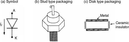
FIGURE 2.1 Power diode: (a) symbol; (b) and (c) types of packaging.
The characteristics of a practical diode show a departure from the ideals of zero forward and infinite reverse impedance, as shown in Fig. 2.2a. In the forward direction, a potential barrier associated with the distribution of charges in the vicinity of the junction, together with other effects, leads to a voltage drop. This, in the case of silicon, is in the range of 1V for currents in the normal range. In reverse, within the normal operating range of voltage, a very small current flows which is largely independent of the voltage. For practical purposes, the static characteristics is often represented by Fig. 2.2b.

FIGURE 2.2a Typical static characteristic of a power diode (forward and reverse have different scale).
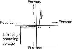
FIGURE 2.2b Practical representation of the static characteristic of a power diode.
In the figure, the forward characteristic is expressed as a threshold voltage Vo and a linear incremental or slope resistance, r. The reverse characteristic remains the same over the range of possible leakage currents irrespective of voltage within the normal working range.
2.2 Properties of PN Junction
From the forward and reverse biased condition characteristics, one can notice that when the diode is forward biased, current rises rapidly as the voltage is increased. Current in the reverse biased region is significantly small until the breakdown voltage of the diode is reached. Once the applied voltage is over this limit, the current will increase rapidly to a very high value limited only by an external resistance.
DC diode parameters. The most important parameters are the followings:
• Forward voltage, VF is the voltage drop of a diode across A and K at a defined current level when it is forward biased.
• Breakdown voltage, VB is the voltage drop across the diode at a defined current level when it is beyond reverse biased level. This is popularly known as avalanche.
• Reverse current IR is the current at a particular voltage, which is below the breakdown voltage.
AC diode parameters. The commonly used parameters are the followings:
• Forward recovery time, tFR is the time required for the diode voltage to drop to a particular value after the forward current starts to flow.
• Reverse recovery time trr is the time interval between the application of reverse voltage and the reverse current dropped to a particular value as shown in Fig. 2.3. Parameter ta is the interval between the zero crossing of the diode current to when it becomes IRR. On the other hand, tb is the time interval from the maximum reverse recovery current to approximately 0.25 of IRR. The ratio of the two parameters ta and tb is known as the softness factor (SF). Diodes with abrupt recovery characteristics are used for high frequency switching.

FIGURE 2.3 Diode reverse recovery with various softness factors.
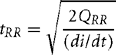
In practice, a design engineer frequently needs to calculate the reverse recovery time. This is in order to evaluate the possibility of high frequency switching. As a thumb rule, the lower tRR the faster the diode can be switched.
![]() (2.1)
(2.1)
If tb is negligible compared to ta which is a very common case, then the following expression is valid:
from which the reverse recovery current
![]()
where QRR is the storage charge and can be calculated from the area enclosed by the path of the recovery current.
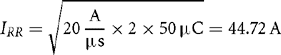
EXAMPLE 2.1 The manufacturer of a selected diode gives the rate of fall of the diode current di/dt= 20A/μs, and its reverse recovery time trr = 5μs. What value of peak reverse current do you expect?
SOLUTION. The peak reverse current is given as:
![]()
The storage charge QRR is calculated as:
![]()
Hence,
• Diode capacitance, CD is the net diode capacitance including the junction (CJ) plus package capacitance (Cp).
In high-frequency pulse switching, a parameter known as transient thermal resistance is of vital importance since it indicates the instantaneous junction temperature as a function of time under constant input power.
2.3 Common Diode Types
Depending on their applications, diodes can be segregated into the following major divisions:
Small signal diode: They are perhaps the most widely used semiconductor devices used in wide variety of applications. In general purpose applications, they are used as a switch in rectifiers, limiters, capacitors, and in wave-shaping. Some common diode parameters a designer needs to know are the forward voltage, reverse breakdown voltage, reverse leakage current, and the recovery time.
Silicon rectifier diode: These are the diodes, which have high forward current carrying capability, typically up to several hundred amperes. They usually have a forward resistance of only a fraction of an ohm while their reverse resistance is in the mega-ohm range. Their primary application is in power conversion, like in power supplies, UPS, rectifiers/inverters, etc.
In case of current exceeding the rated value, their case temperature will rise. For stud-mounted diodes, their thermal resistance is between 0.1 and 1°C/W.
Zener diode: Its primary applications are in the voltage reference or regulation. However, its ability to maintain a certain voltage depends on its temperature coefficient and the impedance. The voltage reference or regulation applications of zener diodes are based on their avalanche properties. In the reverse biased mode, at a certain voltage the resistance of these devices may suddenly drop. This occurs at the zener voltage VX, a parameter the designer knows beforehand.
Figure 2.4 shows a circuit using a zener diode to control a reference voltage of a linear power supply. Under normal operating condition, the transistor will transmit power to the load (output) circuit. The output power level will depend on the transistor base current. A very high base current will impose a large voltage across the zener and it may attain zener voltage VX, when it will crush and limit the power supply to the load.

FIGURE 2.4 Voltage regulator with a zener diode for reference.
Photo diode: When a semiconductor junction is exposed to light, photons generate hole-electron pairs. When these charges diffuse across the junction, they produce photocurrent. Hence this device acts as a source of current, which increases with the intensity of light.
Light emitting diode (LED): Power diodes used in PE circuits are high power versions of the commonly used devices employed in analog and digital circuits. They are manufactured in wide varieties and ranges. The current rating can be from a few amperes to several hundreds while the voltage rating varies from tens of volts to several thousand volts.
2.4 Typical Diode Ratings
2.4.1 Voltage Ratings
For power diodes, a given datasheet has two voltage ratings. One is the repetitive peak inverse voltage (VRRM) the other is the non-repetitive peak inverse voltage. The non-repetitive voltage (VRM) is the diodes capability to block a reverse voltage that may occur occasionally due to a overvoltage surge. Repetitive voltage on the other hand is applied on the diode in a sustained manner. To understand this, let us look at the circuit in Fig. 2.5.

FIGURE 2.5a The circuit.
EXAMPLE 2.2 Two equal source voltages of 220 V peak and phase shifted from each other by 180° are supplying a common load as shown, (a) Show the load voltage; (b) describe when diode D1 will experience VRRM; and (c) determine the VRRM magnitude considering a safety factor of 1.5.
SOLUTION. (a) The input voltage, load voltage, and the voltage across D1 when it is not conducting (VRRM) are shown in Fig. 2.5b.
(b) Diode D1 will experience VRRM when it is not conducting. This happens when the applied voltage V1 across it is in the negative region (from 70 to 80 ms as shown in the figure) and consequently the diode is reverse biased. The actual ideal voltage across it is the peak value of the two input voltages i.e. 220 × 2 = 440 V. This is because when D1 is not conducting, D2 conducts. Hence in addition Van, Vbn is also applied across it since D2 is practically shorted.
(c) The VRRM = 440V is the value in ideal situation. In practice, higher voltages may occur due to stray circuit inductances and/or transients due to the reverserecovery of the diode. They are hard to estimate. Hence, a design engineer would always use a safety factor to cater to these overvoltages. Hence, one should use a diode with a 220 × 2 × 1.5 = 660 V rating.
2.4.2 Current Ratings
Power diodes are usually mounted on a heat sink. This effectively dissipates the heat arising due to continuous conduction. Hence, current ratings are estimated based on temperature rise considerations. The datasheet of a diode normally specifies three different current ratings. They are (1) the average current, (2) the rms current, and (3) the peak current. A design engineer must ensure that each of these values is not exceeded. To do that, the actual current (average, rms, and peak) in the circuit must be evaluated either by calculation, simulation, or measurement. These values must be checked against the ones given in the datasheet for that selected diode. The calculated values must be less than or equal to the datasheet values. The following example shows this technique.
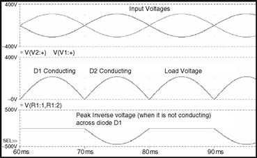
FIGURE 2.5b The waveforms.
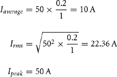
EXAMPLE 2.3 The current waveform passing through a diode switch in a switch mode power supply application is shown in Fig. 2.6. Find the average, rms, and the peak current.
SOLUTION. The current pulse duration is shown to be 0.2 ms within a period of 1 ms and with a peak amplitude of 50 A. Hence the required currents are:
Sometimes, a surge current rating and its permissible duration is also given in a datasheet. For protection of diodes and other semiconductor devices, a fast acting fuse is required. These fuses are selected based on their I2 t rating which is normally specified in a datasheet for a selected diode.
FIGURE 2.6 The current waveform.
2.5 Snubber Circuits for Diode
Snubber circuits are essential for diodes used in switching circuits. It can save a diode from overvoltage spikes, which may arise during the reverse recovery process. A very common snubber circuit for a power diode consists of a capacitor and a resistor connected in parallel with the diode as shown in Fig. 2.7.
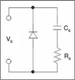
FIGURE 2.7 A typical snubber circuit.
When the reverse recovery current decreases, the capacitor by virtue of its property will try to hold the voltage across it, which, approximately, is the voltage across the diode. The resistor on the other hand will help to dissipate some of the energy stored in the inductor, which forms the IRR loop. The dv/dt across a diode can be calculated as:
![]() (2.2)
(2.2)
where VS is the voltage applied across the diode.
Usually the dv/dt rating of a diode is given in the manufacturers datasheet. Knowing dv/dt and the RS, one can choose the value of the snubber capacitor Cs. The Rs can be calculated from the diode reverse recovery current:
![]() (2.3)
(2.3)
The designed dv/dt value must always be equal or lower than the dv/dt value found from the datasheet.
2.6 Series and Parallel Connection of Power Diodes
For specific applications, when the voltage or current rating of a chosen diode is not enough to meet the designed rating, diodes can be connected in series or parallel. Connecting them in series will give the structure a high voltage rating that may be necessary for high-voltage applications. However, one must ensure that the diodes are properly matched especially in terms of their reverse recovery properties. Otherwise, during reverse recovery there may be a large voltage imbalances between the series connected diodes. Additionally, due to the differences in the reverse recovery times, some diodes may recover from the phenomenon earlier than the other causing them to bear the full reverse voltage. All these problems can effectively be overcome by connecting a bank of a capacitor and a resistor in parallel with each diode as shown in Fig. 2.8.
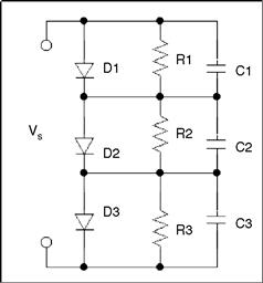
FIGURE 2.8 Series connected diodes with necessary protection.
If a selected diode cannot match the required current rating, one may connect several diodes in parallel. In order to ensure equal current sharing, the designer must choose diodes with the same forward voltage drop properties. It is also important to ensure that the diodes are mounted on similar heat sinks and are cooled (if necessary) equally. This will affect the temperatures of the individual diodes, which in turn may change the forward characteristics of diode.
Tutorial 2.1 Reverse Recovery and Overvoltages
Figure 2.9 shows a simple switch mode power supply. The switch (1-2) is closed at t=0s. When the switch is open, a freewheeling current IF = 20A flows through the load (RL), freewheeling diode (DF), and the large load circuit inductance (LL). The diode reverse recovery current is 20 A and it then decays to zero at the rate of 10A/μs. The load is rated at 10Ω and the forward on-state voltage drop is neglected.
(a) Draw the current waveform during the reverse recovery (IRR) and find its time (trr).
(b) Calculate the maximum voltage across the diode during this process (IRR).
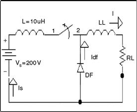
FIGURE 2.9 A simple switch mode power supply with freewheeling diode.
SOLUTION. (a) A typical current waveform during reverse recovery process is shown in Fig. 2.10 for an ideal diode.
When the switch is closed, the steady-state current is, ISS = 200V/10Ω = 20A, since under steady-state condition, the inductor is shorted. When the switch is open, the reverse recovery current flows in the right-hand side loop consisting of the LL, RL, and DE The load inductance, LL is assumed to be shorted. Hence, when the switch is closed, the loop equation is:
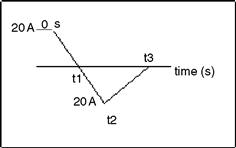
FIGURE 2.10 Current through the freewheeling diode during reverse recovery.
![]()
from which
![]()
At the moment the switch is open, the same current keeps flowing in the right-hand side loop. Hence,
![]()
from time zero to time t1 the current will decay at a rate of 20 A/μs and will be zero at t1 = 20/20 = 1μs. The reverse recovery current starts at this point and, according to the given condition, becomes 20 A at t2. From this point on, the rate of change remains unchanged at 20Aμs. Period t2–t1 is found as:
![]()
From t2 to t3, the current decays to zero at the rate of 20A μs. The required time:
![]()
Hence the actual reverse recovery time: trr = t3 –t1 = (1 + 1 + 2)–1 = 3μs.
(b) The diode experiences the maximum voltage just when the switch is open. This is because both the source voltage 200 V and the newly formed voltage due to the change in current through the inductor L. The voltage across the diode:
![]()
Tutorial 2.2 Ideal Diode Operation, Mathematical Analysis, and PSPICE Simulation
This tutorial illustrates the operation of a diode circuit. Most of the PE applications operate at a relative high voltage, and in such cases, the voltage drop across the power diode usually is small. It is quite often justifiable to use the ideal diode model. An ideal diode has a zero conduction drop when it is forward biased and has zero current when it is reverse biased. The explanation and the analysis presented below is based on the ideal diode model.
Circuit Operation
A circuit with a single diode and an RL load is shown in Fig. 2.11. The source VS is an alternating sinusoidal source. If VS = Esin(ωt), then VS is positive when 0 < ωt < π, and VS is negative when p < ωt < 2π. When VS starts becoming positive, the diode starts conducting and the positive source keeps the diode in conduction till ωt reaches p radians. At that instant, defined by ωt = p radians, the current through the circuit is not zero and there is some energy stored in the inductor. The voltage across an inductor is positive when the current through it is increasing and becomes negative when the current through it tends to fall. When the voltage across the inductor is negative, it is in such a direction as to forward bias the diode. The polarity of voltage across the inductor is as shown in Fig. 2.12 or 2.13.
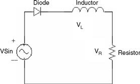
FIGURE 2.11 Circuit diagram.
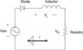
FIGURE 2.12 Current increasing, 0 < ωt < p/2.

FIGURE 2.13 Current decreasing, π/2 < ωt < π.
When VS changes from a positive to a negative value, there is current through the load at the instant ωt = p radians and the diode continues to conduct till the energy stored in the inductor becomes zero. After that the current tends to flow in the reverse direction and the diode blocks conduction. The entire applied voltage now appears across the diode.
Mathematical Analysis
An expression for the current through the diode can be obtained as shown in the equations. It is assumed that the current flows for 0 < ωt < β, where β> π, when the diode conducts, the driving function for the differential equation is the sinusoidal function defining the source voltage. During the period defined by β< ωt < 2π, the diode blocks current and acts as an open switch. For this period, there is no equation defining the behavior of the circuit. For 0 < ωt <β, Eq. (2.4) applies.
![]() (2.4)
(2.4)
Given a linear differential equation, the solution is found out in two parts. The homogeneous equation is defined by Eq. (2.5). It is preferable to express the equation in terms of the angle θ instead “t” Since θ = ωt, we get that dθ = ω.dt. Then Eq. (2.5) gets converted to Eq. (2.6). Equation (2.7) is the solution to this homogeneous equation and is called the complementary integral.
The value of constant A in the complimentary solution is to be evaluated later. The particular solution is the steady-state response and Eq. (2.8) expresses the particular solution. The steady-state response is the current that would flow in steady state in a circuit that contains only the source, resistor, and inductor shown in the circuit, the only element missing being the diode. This response can be obtained using the differential equation or the Laplace transform or the ac sinusoidal circuit analysis. The total solution is the sum of both the complimentary and the particular solution and it is shown in Eq. (2.9). The value of A is obtained using the initial condition. Since the diode starts conducting at ωt = 0 and the current starts building up from zero, i(0) = 0. The value of A is expressed by Eq. (2.10).
Once the value of A is known, the expression for current is known. After evaluating A, current can be evaluated at different values of ωt, starting from ωt = π. As ωt increases, the current would keep decreasing. For some values of ωt, say β, the current would be zero. If ωt >β the current would evaluate to a negative value. Since the diode blocks current in the reverse direction, the diode stops conducting when ωt reaches. Then an expression for the average output voltage can be obtained. Since the average voltage across the inductor has to be zero, the average voltage across the resistor and average voltage at the cathode of the diode are the same. This average value can be obtained as shown in Eq. (2.11).
![]() (2.8)
(2.8)
where
![]()
![]() (2.9)
(2.9)
![]() (2.10)
(2.10)
Hence, the average output voltage:
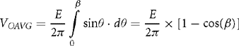 (2.11)
PSPICE Simulation
For simulation using PSPICE, the circuit used is shown in Fig. 2.14. Here the nodes are numbered. The ac source is connected between the nodes 1 and 0. The diode is connected between the nodes 1 and 2 and the inductor links the nodes 2 and 3. The resistor is connected from the node 3 to the reference node, that is, node 0. The circuit diagram is shown in Fig. 2.14.
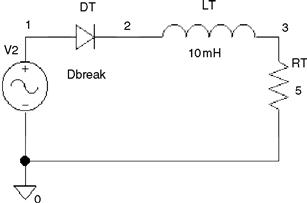
FIGURE 2.14 PSPICE model to study an R-L diode circuit.
The PSPICE program in textform is presented below.
* Half-wave Rectifier with RL Load
* An exercise to find the diode current
.MODEL Dbreak D(IS=10N N=1 BV=1200
.TRAN 10 uS 100 mS 60 mS 100 uS
The diode is described using the MODEL statement. The TRAN statement simulates the transient operation for a period of 100 ms at an interval of 10 ms. The OPTIONS statement sets limits for tolerances. The output can be viewed on the screen because of the PROBE statement. A snapshot of various voltages/currents is shown in Fig. 2.15.
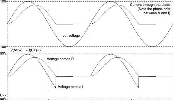
FIGURE 2.15 Voltage/current waveforms at various points in the circuit.
From Fig. 2.15, it is evident that the current lags the source voltage. This is a typical phenomenon in any inductive circuit and is associated with the energy storage property of the inductor. This property of the inductor causes the current to change slowly, governed by the time constant τ = tan− 1 (ωl/R). Analytically, this is calculated by the expression in Eq. (2.8).
2.7 Typical Applications of Diodes
A. In rectification
Four diodes can be used to fully rectify an ac signal as shown in Fig. 2.16. Apart from other rectifier circuits, this topology does not require an input transformer. However, they are used for isolation and protection. The direction of the current is decided by two diodes conducting at any given time. The direction of the current through the load is always the same. This rectifier topology is known as the full bridge rectifier.
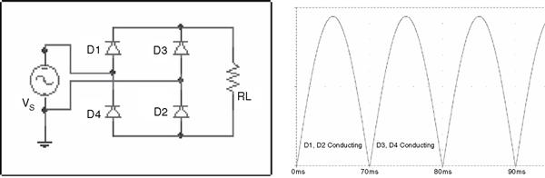
FIGURE 2.16 Full bridge rectifier and its output dc voltage.
The average rectifier output voltage:
![]()
The rms rectifier output voltage:
![]()
This rectifier is twice as efficient as compared to a single phase one.
B. For voltage clamping
Figure 2.17 shows a voltage clamper. The negative pulse of the sinusoidal input voltage charges the capacitor to its maximum value in the direction shown. After charging, the capacitor cannot discharge, since it is open circuited by the diode. Hence the output voltage:
![]()
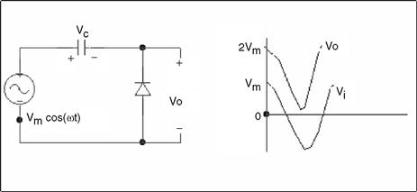
FIGURE 2.17 Voltage clamping with diode.
The output voltage is clamped between zero and 2Vm.
C. As voltage multiplier
Connecting diode in a predetermined manner, an ac signal can be doubled, tripled, and even quadrupled. This is shown in Fig. 2.18. As evident, the circuit will yield a dc voltage equal to 2Vm. The capacitors are alternately charged to the maximum value of the input voltage.
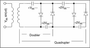
FIGURE 2.18 Voltage doubler and quadrupler circuit.
2.8 Standard Datasheet for Diode Selection
In order for a designer to select a diode switch for specific applications, the following tables and standard test results can be used. A power diode is primarily chosen based on forward current (IF) and the peak inverse (VRRM) voltage. For example, the designer chooses the diode type V30 from the table in Fig. 2.19 because it closely matches their calculated values of IF and VRRM without going over. However, if for some reason only the VRRM matches but the calculated value of IF comes higher, one should go for diode H14, and so on. Similar concept is used for VRRM.
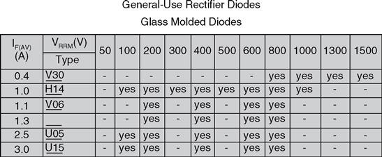
FIGURE 2.19 Table of diode selection based on average forward current, IF(AV) and peak inverse voltage, VRRM (courtesy of Hitachi semiconductors).
In addition to the above mentioned diode parameters, one should also calculate parameters like the peak forward voltage, reverse recovery time, case and junction temperatures, etc. and check them against the datasheet values. Some of these datasheet values are provided in Fig. 2.20 for the selected diode V30. Figures 2.21–2.23 give the standard experimental relationships between voltages, currents, power, and case temperatures for our selected V30 diode. These characteristics help a designer to understand the safe operating area for the diode, and to make a decision whether or not to use a snubber or a heat sink. If one is particularly interested in the actual reverse recovery time measurement, the circuit given in Fig. 2.24 can be constructed and experimented upon.

FIGURE 2.20 Details of diode characteristics for diode V30 selected from Fig. 2.19.
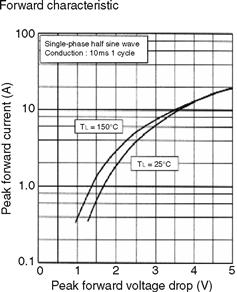
FIGURE 2.21 Variation of peak forward voltage drop with peak forward current.
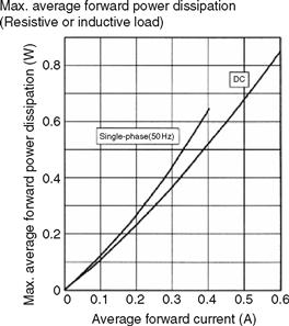
FIGURE 2.22 Variation of maximum forward power dissipation with average forward current.
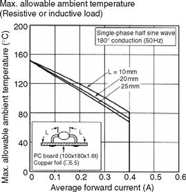
FIGURE 2.23 Maximum allowable case temperature with variation of average forward current.
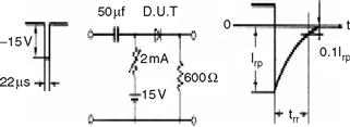
FIGURE 2.24 Reverse recovery time (trr) measurement.
REFERENCES
1. Lurch N. Fundamentals of Electronics. 3rd ed. New York: John Wiley & Sons Ltd.; 1981.
2. Tartar R. Solid-State Power Conversion Handbook. New York: John Wiley & Sons Ltd.; 1993.
3. Marston RM. Power Control Circuits Manual. Newnes circuits manual series. New York: Butterworth Heinemann Ltd.; 1995.
4. Hitachi Semiconductor Devices. http://semiconductor.hitachi.com.. [Internet information on].
5. International rectifier. Power Semiconductors Product Digest. 1992/93.
6. Electronic Devices & SMPS Books. http://www.smpstech.com/books/booklist.htm.. [Internet information on].