
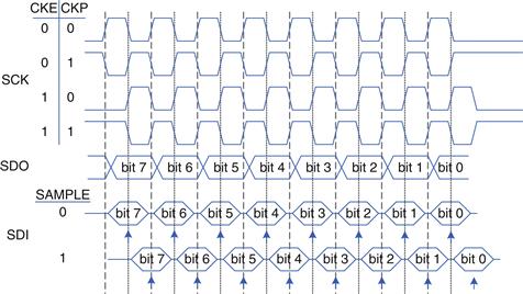
Figure 8.39 Clock and data timing controlled by CKE, CKP, and SAMPLE
Universal Asynchronous Receiver Transmitter (UART)
A UART (pronounced “you-art”) is a serial I/O peripheral that communicates between two systems without sending a clock. Instead, the systems must agree in advance about what data rate to use and must each locally generate its own clock. Although these system clocks may have a small frequency error and an unknown phase relationship, the UART manages reliable asynchronous communication. UARTs are used in protocols such as RS-232 and RS-485. For example, computer serial ports use the RS-232C standard, introduced in 1969 by the Electronic Industries Association. The standard originally envisioned connecting Data Terminal Equipment (DTE) such as a mainframe computer to Data Communication Equipment (DCE) such as a modem. Although a UART is relatively slow compared to SPI, the standards have been around for so long that they remain important today.
Figure 8.40(a) shows an asynchronous serial link. The DTE sends data to the DCE over the TX line and receives data back over the RX line. Figure 8.40(b) shows one of these lines sending a character at a data rate of 9600 baud. The line idles at a logic ‘1’ when not in use. Each character is sent as a start bit (0), 7-8 data bits, an optional parity bit, and one or more stop bits (1’s). The UART detects the falling transition from idle to start to lock on to the transmission at the appropriate time. Although seven data bits is sufficient to send an ASCII character, eight bits are normally used because they can convey an arbitrary byte of data.
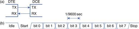
Figure 8.40 Asynchronous serial link
An additional bit, the parity bit, can also be sent, allowing the system to detect if a bit was corrupted during transmission. It can be configured as even or odd; even parity means that the parity bit is chosen such that the total collection of data and parity has an even number of 1’s; in other words, the parity bit is the XOR of the data bits. The receiver can then check if an even number of 1’s was received and signal an error if not. Odd parity is the reverse and is hence the XNOR of the data bits.
A common choice is 8 data bits, no parity, and 1 stop bit, making a total of 10 symbols to convey an 8-bit character of information. Hence, signaling rates are referred to in units of baud rather than bits/sec. For example, 9600 baud indicates 9600 symbols/sec, or 960 characters/sec, giving a data rate of 960 × 8 = 7680 data bits/sec. Both systems must be configured for the appropriate baud rate and number of data, parity, and stop bits or the data will be garbled. This is a hassle, especially for nontechnical users, which is one of the reasons that the Universal Serial Bus (USB) has replace UARTs in personal computer systems.
Typical baud rates include 300, 1200, 2400, 9600, 14400, 19200, 38400, 57600, and 115200. The lower rates were used in the 1970’s and 1980’s for modems that sent data over the phone lines as a series of tones. In contemporary systems, 9600 and 115200 are two of the most common baud rates; 9600 is encountered where speed doesn’t matter, and 115200 is the fastest standard rate, though still slow compared to other modern serial I/O standards.
In the 1950s through 1970s, early hackers calling themselves phone phreaks learned to control the phone company switches by whistling appropriate tones. A 2600 Hz tone produced by a toy whistle from a Cap’n Crunch cereal box (Figure 8.41) could be exploited to place free long-distance and international calls.
Figure 8.41 Cap’n Crunch Bosun Whistle.
Photograph by Evrim Sen, reprinted with permission.
The RS-232 standard defines several additional signals. The Request to Send (RTS) and Clear to Send (CTS) signals can be used for hardware handshaking. They can be operated in either of two modes. In flow control mode, the DTE clears RTS to 0 when it is ready to accept data from the DCE. Likewise, the DCE clears CTS to 0 when it is ready to receive data from the DTE. Some datasheets use an overbar to indicate that they are active-low. In the older simplex mode, the DTE clears RTS to 0 when it is ready to transmit. The DCE replies by clearing CTS when it is ready to receive the transmission.
Some systems, especially those connected over a telephone line, also use Data Terminal Ready (DTR), Data Carrier Detect (DCD), Data Set Ready (DSR), and Ring Indicator (RI) to indicate when equipment is connected to the line.
The original standard recommended a massive 25-pin DB-25 connector, but PCs streamlined to a male 9-pin DE-9 connector with the pinout shown in Figure 8.42(a). The cable wires normally connect straight across as shown in Figure 8.42(b). However, when directly connecting two DTEs, a null modem cable shown in Figure 8.42(c) may be needed to swap RX and TX and complete the handshaking. As a final insult, some connectors are male and some are female. In summary, it can take a large box of cables and a certain amount of guess-work to connect two systems over RS-232, again explaining the shift to USB. Fortunately, embedded systems typically use a simplified 3- or 5-wire setup consisting of GND, TX, RX, and possibly RTS and CTS.
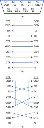
Figure 8.42 DE-9 male cable (a) pinout, (b) standard wiring, and (c) null modem wiring
Handshaking refers to the negotiation between two systems; typically, one system signals that it is ready to send or receive data, and the other system acknowledges that request.
RS-232 represents a 0 electrically with 3 to 15 V and a 1 with −3 to −15 V; this is called bipolar signaling. A transceiver converts the digital logic levels of the UART to the positive and negative levels expected by RS-232, and also provides electrostatic discharge protection to protect the serial port from damage when the user plugs in a cable. The MAX3232E is a transceiver compatible with both 3.3 and 5 V digital logic. It contains a charge pump that, in conjunction with external capacitors, generates ± 5 V outputs from a single low-voltage power supply.
The PIC32 has six UARTs named U1-U6. As with SPI, the PIC® program must first configure the port. Unlike SPI, reading and writing can occur independently because either system may transmit without receiving and vice versa. Each UART is associated with five 32-bit registers: UxMODE, UxSTA (status), UxBRG, UxTXREG, and UxRXREG. For example, U1MODE is the mode register for UART1. The mode register is used to configure the UART and the STA register is used to check when data is available. The BRG register is used to set the baud rate. Data is transmitted or received by writing the TXREG or reading the RXREG.
The MODE register defaults to 8 data bits, 1 stop bit, no parity, and no RTS/CTS flow control, so for most applications the programmer is only interested in bit 15, the ON bit, which enables the UART.
The STA register contains bits to enable the transmit and receive pins and to check if the transmit and receive buffers are full. After setting the ON bit of the UART, the programmer must also set the UTXEN and URXEN bits (bits 10 and 12) of the STA register to enable these two pins. UTXBF (bit 9) indicates that the transmit buffer is full. URXDA (bit 0) indicates that the receive buffer has data available. The STA register also contains bits to indicate parity and framing errors; a framing error occurs if the start or stop bits aren’t found at the expected time.
The 16-bit BRG register is used to set the baud rate to a fraction of the peripheral bus clock.
![]() (8.4)
(8.4)
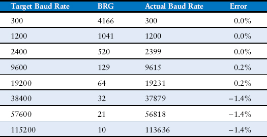
Table 8.7 lists settings of BRG for common target baud rates assuming a 20 MHz peripheral clock. It is sometimes impossible to reach exactly the target baud rate. However, as long as the frequency error is much less than 5%, the phase error between the transmitter and receiver will remain small over the duration of a 10-bit frame so data is received properly. The system will then resynchronize at the next start bit.
Table 8.7 BRG settings for a 20 MHz peripheral clock
To transmit data, wait until STA.UTXBF is clear indicating that the transmit buffer has space available, and then write the byte to TXREG. To receive data, check STA.URXDA to see if data has arrived, and then read the byte from the RXREG.
Example 8.20 Serial Communication with a PC
Develop a circuit and a C program for a PIC32 to communicate with a PC over a serial port at 115200 baud with 8 data bits, 1 stop bit, and no parity. The PC should be running a console program such as PuTTY3 to read and write over the serial port. The program should ask the user to type a string. It should then tell the user what she typed.
Solution
Figure 8.43 shows a schematic of the serial link. Because few PCs still have physical serial ports, we use a Plugable USB to RS-232 DB9 Serial Adapter from plugable.com shown in Figure 8.44 to provide a serial connection to the PC. The adapter connects to a female DE-9 connector soldered to wires that feed a transceiver, which converts the voltages from the bipolar RS-232 levels to the PIC32 microcontroller’s 3.3 V level. For this example, we chose UART2 on the PIC32. The microcontroller and PC are both Data Terminal Equipment, so the TX and RX pins must be cross-connected in the circuit. The RTS/CTS handshaking from the PIC32 is not used, and the RTS and CTS on the DE9 connector are tied together so that the PC will shake its own hand.

Figure 8.43 PIC32 to PC serial link

Figure 8.44 Plugable USB to RS-232 DB9 Serial Adapter
© 2012 Plugable Technologies; reprinted with permission
To configure PuTTY to work with the serial link, set Connection type to Serial and Speed to 115200. Set Serial line to the COM port assigned by the operating system to the Serial to USB Adapter. In Windows, this can be found in the Device Manager; for example, it might be COM3. Under the Connection → Serial tab, set flow control to NONE or RTS/CTS. Under the Terminal tab, set Local Echo to Force On to have characters appear in the terminal as you type them.
The code is listed below. The Enter key in the terminal program corresponds to a carriage return character called ’ ’ in C with an ASCII code of 0x0D. To advance to the beginning of the next line when printing, send both the ’ ’ and ’ ’ (new line and carriage return) characters.4
The functions to initialize, read, and write the serial port make up a simple device driver. The device driver offers a level of abstraction and modularity between the programmer and the hardware, so that a programmer using the device driver doesn’t have to understand the UART’s register set. It also simplifies moving the code to a different microcontroller; the device driver must be rewritten but the code that calls it can remain the same.
The main function demonstrates printing to the console and reading from the console using the putstrserial and getstrserial functions. It also demonstrates using printf, from stdio.h, which automatically prints through UART2. Unfortunately, the PIC32 libraries do not presently support scanf over the UART in a graceful way, but getstrserial is sufficient.
#include <P32xxxx.h>
#include <stdio.h>
void inituart(void) {
U2STAbits.UTXEN = 1; // enable transmit pin
U2STAbits.URXEN = 1; // enable receive pin
U2BRG = 10; // set baud rate to 115.2k
U2MODEbits.ON = 1; // enable UART
}
char getcharserial(void) {
while (!U2STAbits.URXDA); // wait until data available
return U2RXREG; // return character received from
// serial port
}
void getstrserial(char *str) {
int i = 0;
do { // read an entire string until detecting
str[i] = getcharserial(); // carriage return
} while (str[i++] != ’ ’); // look for carriage return
str[i−1] = 0; // null-terminate the string
}
void putcharserial(char c) {
while (U2STAbits.UTXBF); // wait until transmit buffer empty
U2TXREG = c; // transmit character over serial port
}
void putstrserial(char *str) {
int i = 0;
while (str[i] != 0) { // iterate over string
putcharserial(str[i++]); // send each character
}
}
int main(void) {
char str[80];
inituart();
while(1) {
putstrserial("Please type something: ");
getstrserial(str);
printf(" You typed: %s ", str);
}
}
Communicating with the serial port from a C program on a PC is a bit of a hassle because serial port driver libraries are not standardized across operating systems. Other programming environments such as Python, Matlab, or LabVIEW make serial communication painless.
8.6.4 Timers
Embedded systems commonly need to measure time. For example, a microwave oven needs a timer to keep track of the time of day and another to measure how long to cook. It might use yet another to generate pulses to the motor spinning the platter, and a fourth to control the power setting by only activating the microwave’s energy for a fraction of every second.
The PIC32 has five 16-bit timers on board. Timer1 is called a Type A timer that can accept an asynchronous external clock source, such as a 32 KHz watch crystal. Timers 2/3 and 4/5 are Type B timers. They run synchronously off the peripheral clock and can be paired (e.g., 2 with 3) to form 32-bit timers for measuring long periods of time.
Each timer is associated with three 16-bit registers: TxCON, TMRx, and PRx. For example, T1CON is the control register for Timer 1. CON is the control register. TMR contains the current time count. PR is the period register. When a timer reaches the specified period, it rolls back to 0 and sets the TxIF bit in the IFS0 interrupt flag register. A program can poll this bit to detect overflow. Alternatively, it can generate an interrupt.
By default, each timer acts as a 16-bit counter accumulating ticks of the internal peripheral clock (20 MHz in our example). Bit 15 of the CON register, called the ON bit, starts the timer counting. The TCKPS bits of the CON register specify the prescalar, as given in Tables 8.8 and 8.9 for Type A and Type B counters. Prescaling by k:1 causes the timer to only count once every k ticks; this can be useful to generate longer time intervals, especially when the peripheral clock is running fast. The other CON register bits are slightly different for Type A and Type B counters; see the datasheet for details.
Table 8.8 Prescalars for Type A timers
| TCKPS[1:0] | Prescale |
| 00 | 1:1 |
| 01 | 8:1 |
| 10 | 64:1 |
| 11 | 256:1 |
Table 8.9 Prescalars for Type B timers
| TCKPS[2:0] | Prescale |
| 000 | 1:1 |
| 001 | 2:1 |
| 010 | 4:1 |
| 011 | 8:1 |
| 100 | 16:1 |
| 101 | 32:1 |
| 110 | 64:1 |
| 111 | 256:1 |
Example 8.21 Delay Generation
Write two functions that create delays of a specified number of microseconds and milliseconds using Timer1. Assume that the peripheral clock is running at 20 MHz.
Solution
Each microsecond is 20 peripheral clock cycles. We empirically observe with an oscilloscope that the delaymicros function has an overhead of approximately 6 μs for the function call and timer initialization. Therefore, we set PR to 20 × (micros – 6). Thus, the function will be inaccurate for durations less than 6 μs. The check at the start prevents overflow of the 16-bit PR.
The delaymillis function repeatedly invokes delaymicros(1000) to create an appropriate number of 1 ms delays.
#include <P32xxxx.h>
void delaymicros(int micros) {
if (micros > 1000) { // avoid timer overflow
delaymicros(1000);
delaymicros(micros-1000);
}
else if (micros > 6){
TMR1 = 0; // reset timer to 0
T1CONbits.ON = 1; // turn timer on
PR1 = (micros-6)*20; // 20 clocks per microsecond.
// Function has overhead of ~6 us
IFS0bits.T1IF = 0; // clear overflow flag
while (!IFS0bits.T1IF); // wait until overflow flag is set
}
}
void delaymillis(int millis) {
while (millis--) delaymicros(1000); // repeatedly delay 1 ms until done
}
Another handy timer feature is gated time accumulation, in which the timer only counts while an external pin is high. This allows the timer to measure the duration of an external pulse. It is enabled using the CON register.
8.6.5 Interrupts
Timers are often used in conjunction with interrupts so that a program may go about its usual business and then periodically handle a task when the timer generates an interrupt. Section 6.7.2 described MIPS interrupts from the architectural point of view. This section explores how to use them in a PIC32.
Interrupt requests occur when a hardware event occurs, such as a timer overflowing, a character being received over a UART, or certain GPIO pins toggling. Each type of interrupt request sets a specific bit in the Interrupt Flag Status (IFS) registers. The processor then checks the corresponding bit in the Interrupt Enable Control (IEC) registers. If the bit is set, the microcontroller should respond to the interrupt request by invoking an interrupt service routine (ISR). The ISR is a function with void arguments that handles the interrupt and clears the bit of the IFS before returning. The PIC32 interrupt system supports single and multi-vector modes. In single-vector mode, all interrupts invoke the same ISR, which must examine the CAUSE register to determine the reason for the interrupt (if multiple types of interrupts may occur) and handle it accordingly. In multi-vector mode, each type of interrupt calls a different ISR. The MVEC bit in the INTCON register determines the mode. In any case, the MIPS interrupt system must be enabled with the ei instruction before it will accept any interrupts.
The PIC32 also allows each interrupt source to have a configurable priority and subpriority. The priority is in the range of 0–7, with 7 being highest. A higher priority interrupt will preempt an interrupt presently being handled. For example, suppose a UART interrupt is set to priority 5 and a timer interrupt is set to priority 7. If the program is executing its normal flow and a character appears on the UART, an interrupt will occur and the microcontroller can read the data from the UART and handle it. If a timer overflows while the UART ISR is active, the ISR will itself be interrupted so that the microcontroller can immediately handle the timer overflow. When it is done, it will return to finish the UART interrupt before returning to the main program. On the other hand, if the timer interrupt had priority 2, the UART ISR would complete first, then the timer ISR would be invoked, and finally the microcontroller would return to the main program.
The subpriority is in the range of 0–3. If two events with the same priority are simultaneously pending, the one with the higher subpriority will be handled first. However, the subpriority will not cause a new interrupt to preempt an interrupt of the same priority presently being serviced. The priority and subpriority of each event is configured with the IPC registers.
Each interrupt source has a vector number in the range of 0–63. For example, the Timer1 overflow interrupt is vector 4, the UART2 RX interrupt is vector 32, and the INT0 external interrupt triggered by a change on pin RD0 is vector 3. The fields of the IFS, IEC, and IPC registers corresponding to that vector number are specified in the PIC32 datasheet.
The ISR function declaration is tagged by two special _ _attribute_ _ directives indicating the priority level and vector number. The compiler uses these attributes to associate the ISR with the appropriate interrupt request. The Microchip MPLAB® C Compiler For PIC32 MCUs User’s Guide has more information about writing interrupt service routines.
Example 8.22 Periodic Interrupts
Write a program that blinks an LED at 1 Hz using interrupts.
Solution
We will set Timer1 to overflow every 0.5 seconds and toggle the LED between ON and OFF in the interrupt handler.
The code below demonstrates the multi-vector mode of operation, even though only the Timer1 interrupt is actually enabled. The blinkISR function has attributes indicating that it has priority level 7 (IPL7) and is for vector 4 (the Timer 1 overflow vector). The ISR toggles the LED and clears the Timer1 Interrupt Flag (T1IF) bit of IFS0 before returning.
The initTimer1Interrupt function sets up the timer to a period of ½ second using a 256:1 prescalar and a count of 39063 ticks. It enables multi-vector mode. The priority and subpriority are specified in bits 4:2 and 1:0 of the IPC1 register, respectively. The Timer 1 interrupt flag (T1IF, bit 4 of IFS0) is cleared and the Timer1 interrupt enable (T1IE, bit 4 of IEC0) is set to accept interrupts from Timer 1. Finally, the asm directive is used to generate the ei instruction to enable the interrupt system.
The main function just waits in a while loop after initializing the timer interrupt. However, it could do something more interesting such as play a game with the user, and yet the interrupt will still ensure that the LED blinks at the correct rate.
#include <p32xxxx.h>
// The Timer 1 interrupt is Vector 4, using enable bit IEC0<4>
// and flag bit IFS0<4>, priority IPC1<4:2>, subpriority IPC1<1:0>
void _ _attribute_ _((interrupt(IPL7))) _ _attribute_ _((vector(4))) blinkISR(void) {
PORTDbits.RD0 = !PORTDbits.RD0; // toggle the LED
IFS0bits.T1IF = 0; // clear the interrupt flag
return;
}
void initTimer1Interrupt(void) {
T1CONbits.ON = 0; // turn timer off
TMR1 = 0; // reset timer to 0
T1CONbits.TCKPS = 3; // 1:256 prescale: 20 MHz / 256 = 78.125 KHz
PR1 = 39063; // toggle every half-second (one second period)
INTCONbits.MVEC = 1; // enable multi-vector mode - we’re using vector 4
IPC1 = 0x7 << 2 | 0x3; // priority 7, subpriority 3
IFS0bits.T1IF = 0; // clear the Timer 1 interrupt flag
IEC0bits.T1IE = 1; // enable the Timer 1 interrupt
asm volatile("ei"); // enable interrupts on the micro-controller
T1CONbits.ON = 1; // turn timer on
}
int main(void) {
TRISD = 0; // set up PORTD to drive LEDs
PORTD = 0;
initTimer1Interrupt();
while(1); // just wait, or do something useful here
}
8.6.6 Analog I/O
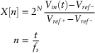
The real world is an analog place. Many embedded systems need analog inputs and outputs to interface with the world. They use analog-to-digital-converters (ADCs) to quantize analog signals into digital values, and digital-to-analog-converters (DACs) to do the reverse. Figure 8.45 shows symbols for these components. Such converters are characterized by their resolution, dynamic range, sampling rate, and accuracy. For example, an ADC might have N = 12-bit resolution over a range Vref− to Vref+ of 0–5 V with a sampling rate of fs = 44 KHz and an accuracy of ± 3 least significant bits (lsbs). Sampling rates are also listed in samples per second (sps), where 1 sps = 1 Hz. The relationship between the analog input voltage Vin(t) and the digital sample X[n] is
 (8.5)
(8.5)
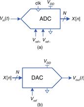
Figure 8.45 ADC and DAC symbols
For example, an input voltage of 2.5 V (half of full scale) would correspond to an output of 1000000000002 = 80016, with an uncertainty of up to 3 lsbs.
Similarly, a DAC might have N = 16-bit resolution over a full-scale output range of Vref = 2.56 V. It produces an output of
![]() (8.6)
(8.6)
Many microcontrollers have built-in ADCs of moderate performance. For higher performance (e.g., 16-bit resolution or sampling rates in excess of 1 MHz), it is often necessary to use a separate ADC connected to the microcontroller. Fewer microcontrollers have built-in DACs, so separate chips may also be used. However, microcontrollers often simulate analog outputs using a technique called pulse-width modulation (PWM). This section describes such analog I/O in the context of the PIC32 microcontroller.
A/D Conversion
The PIC32 has a 10-bit ADC with a maximum speed of 1 million samples/sec (Msps). The ADC can connect to any of 16 analog input pins via an analog multiplexer. The analog inputs are called AN0-15 and share their pins with digital I/O port RB. By default, Vref+ is the analog VDD pin and Vref− is the analog GND pin; in our system, these are 3.3 and 0 V, respectively. The programmer must initialize the ADC, specify which pin to sample, wait long enough to sample the voltage, start the conversion, wait until it finishes, and read the result.
The ADC is highly configurable, with the ability to automatically scan through multiple analog inputs at programmable intervals and to generate interrupts upon completion. This section simply describes how to read a single analog input pin; see the PIC32 Family Reference Manual for details on the other features.
The ADC is controlled by a host of registers: AD1CON1-3, AD1CHS, AD1PCFG, AD1CSSL, and ADC1BUF0-F. AD1CON1 is the primary control register. It has an ON bit to enable the ADC, a SAMP bit to control when sampling and conversion takes place, and a DONE bit to indicate conversion complete. AD1CON3 has ADCS[7:0] bits that control the speed of the A/D conversion. AD1CHS is the channel selection register specifying the analog input to sample. AD1PCFG is the pin configuration register. When a bit is 0, the corresponding pin acts as an analog input. When it is a 1, the pin acts as a digital input. ADC1BUF0 holds the 10-bit conversion result. The other registers are not required in our simple example.
Note that the ADC has a confusing use of the terms sampling rate and sampling time. The sampling time, also called the acquisition time, is the amount of time necessary for the input to settle before conversion takes place. The sampling rate is the number of samples taken per second. It is at most 1/(sampling time + 12 TAD).
The ADC uses a successive approximation register that produces one bit of the result on each ADC clock cycle. Two additional cycles are required, for a total of 12 ADC clocks/conversion. The ADC clock period TAD must be at least 65 ns for correct operation. It is set as a multiple of the peripheral clock period TPB using the ADCS bits according to the relation:
![]() (8.7)
(8.7)
Hence, for peripheral clocks up to 30 MHz, the ADCS bits can be left at their default value of 0.
The sampling time is the amount of time necessary for a new input to stabilize before its conversion can start. As long as the resistance of the source being sampled is less than 5 KΩ, the sampling time can be as small as 132 ns, which is only a small number of clock cycles.
Example 8.23 Analog Input
Write a program to read the analog value on the AN11 pin.
Solution
The initadc function initializes the ADC and selects the specified channel. It leaves the ADC in sampling mode. The readadc function ends sampling and starts the conversion. It waits until the conversion is done, then resumes sampling and returns the conversion result.
#include <P32xxxx.h>
void initadc(int channel) {
AD1CHSbits.CH0SA = channel; // select which channel to sample
AD1PCFGCLR = 1 << channel; // configure pin for this channel to
// analog input
AD1CON1bits.ON = 1; // turn ADC on
AD1CON1bits.SAMP = 1; // begin sampling
AD1CON1bits.DONE = 0; // clear DONE flag
}
int readadc(void) {
AD1CON1bits.SAMP = 0; // end sampling, start conversion
while (!AD1CON1bits.DONE); // wait until done converting
AD1CON1bits.SAMP = 1; // resume sampling to prepare for next
// conversion
AD1CON1bits.DONE = 0; // clear DONE flag
return ADC1BUF0; // return conversion result
}
int main(void) {
int sample;
initadc(11);
sample = readadc();
}
D/A Conversion
The PIC32 has no built-in DAC, so this section describes D/A conversion using external DACs. It also illustrates interfacing the PIC32 to other chips over the parallel and serial ports. The same approach could be used to interface the PIC32 to a higher resolution or faster external ADC.
Some DACs accept the N-bit digital input on a parallel interface with N wires, while others accept it over a serial interface such as SPI. Some DACs require both positive and negative power supply voltages, while others operate off of a single supply. Some support a flexible range of supply voltages, while others demand a specific voltage. The input logic levels should be compatible with the digital source. Some DACs produce a voltage output proportional to the digital input, while others produce a current output; an operational amplifier may be needed to convert this current to a voltage in the desired range.
In this section, we use the Analog Devices AD558 8-bit parallel DAC and the Linear Technology LTC1257 12-bit serial DAC. Both produce voltage outputs, run off a single 5-15 V power supply, use VIH = 2.4 V such that they are compatible with 3.3 V outputs from the PIC32, come in DIP packages that make them easy to breadboard, and are easy to use. The AD558 produces an output on a scale of 0-2.56 V, consumes 75 mW, comes in a 16-pin package, and has a 1 μs settling time permitting an output rate of 1 Msample/sec. The datasheet is at analog.com. The LTC1257 produces an output on a scale of 0-2.048V, consumes less than 2 mW, comes in an 8-pin package, and has a 6 μs settling time. Its SPI operates at a maximum of 1.4 MHz. The datasheet is at linear.com. Texas Instruments is another leading ADC and DAC manufacturer.
Example 8.24 Analog Output with External DACs
Sketch a circuit and write the software for a simple signal generator producing sine and triangle waves using a PIC32, an AD558, and an LTC1257.
Solution
The circuit is shown in Figure 8.46. The AD558 connects to the PIC32 via the RD 8-bit parallel port. It connects Vout Sense and Vout Select to Vout to set the 2.56 V full-scale output range. The LTC1257 connects to the PIC32 via SPI2. Both ADCs use a 5 V power supply and have a 0.1 μF decoupling capacitor to reduce power supply noise. The active-low chip enable and load signals on the DACs indicate when to convert the next digital input. They should be held high while a new input is being loaded.

Figure 8.46 DAC parallel and serial interfaces to a PIC32
The program is shown below. initio initializes the parallel and serial ports and sets up a timer with a period to produce the desired output frequency. The SPI is set to 16-bit mode at 1 MHz, but the LTC1257 only cares about the last 12 bits sent. initwavetables precomputes an array of sample values for the sine and triangle waves. The sine wave is set to a 12-bit scale and the triangle to an 8-bit scale. There are 64 points per period of each wave; changing this value trades precision for frequency. genwaves cycles through the samples. For each sample, it disables the CE and LOAD signals to the DACs, sends the new sample over the parallel and serial ports, reenables the DACs, and then waits until the timer indicates that it is time for the next sample. The minimum sine and triangle wave frequency of 5 Hz is set by the 16-bit Timer1 period register, and the maximum frequency of 605 Hz (38.7 Ksamples/sec) is set by the time to send each point in the genwaves function, of which the SPI transmission is a major component.
#include <P32xxxx.h>
#include <math.h> // required to use the sine function
#define NUMPTS 64
int sine[NUMPTS], triangle[NUMPTS];
void initio(int freq) { // freq can be 5-605 Hz
TRISD = 0xFF00; // make the bottom 8 bits of PORT D outputs
SPI2CONbits.ON = 0; // disable SPI to reset any previous state
SPI2BRG = 9; // 1 MHz SPI clock
SPI2CONbits.MSTEN = 1; // enable master mode
SPI2CONbits.CKE = 1; // set clock-to-data timing
SPI2CONbits.MODE16 = 1; // activate 16-bit mode
SPI2CONbits.ON = 1; // turn SPI on
TRISF = 0xFFFE; // make RF0 an output to control load and ce
PORTFbits.RF0 = 1; // set RF0 = 1
PR1 = (20e6/NUMPTS)/freq - 1; // set period register for desired wave
// frequency
T1CONbits.ON = 1; // turn Timer1 on
}
void initwavetables(void) {
int i;
for (i=0; i<NUMPTS; i++) {
sine[i] = 2047*(sin(2*3.14159*i/NUMPTS) + 1); // 12-bit scale
if (i<NUMPTS/2) triangle[i] = i*511/NUMPTS; // 8-bit scale
else triangle[i] = 510-i*511/NUMPTS;
}
}
void genwaves(void) {
int i;
while (1) {
for (i=0; i<NUMPTS; i++) {
IFS0bits.T1IF = 0; // clear timer overflow flag
PORTFbits.RF0 = 1; // disable load while inputs are changing
SPI2BUF = sine[i]; // send current points to the DACs
PORTD = triangle[i];
while (SPI2STATbits.SPIBUSY); // wait until transfer completes
PORTFbits.RF0 = 0; // load new points into DACs
while (!IFS0bits.T1IF); // wait until time to send next point
}
}
}
int main(void) {
initio(500);
initwavetables();
genwaves();
}
Pulse-Width Modulation
Another way for a digital system to generate an analog output is with pulse-width modulation (PWM), in which a periodic output is pulsed high for part of the period and low for the remainder. The duty cycle is the fraction of the period for which the pulse is high, as shown in Figure 8.47. The average value of the output is proportional to the duty cycle. For example, if the output swings between 0 and 3.3 V and has a duty cycle of 25%, the average value will be 0.25 × 3.3 = 0.825 V. Low-pass filtering a PWM signal eliminates the oscillation and leaves a signal with the desired average value.

Figure 8.47 Pulse-width modulated (PWM) signal
The PIC32 contains five output compare modules, OC1-OC5, that each, in conjunction with Timer 2 or 3, can produce PWM outputs.5 Each output compare module is associated with three 32-bit registers: OCxCON, OCxR, and OCxRS. CON is the control register. The OCM bits of the CON register should be set to 1102 to activate PWM mode, and the ON bit should be enabled. By default, the output compare uses Timer2 in 16-bit mode, but the OCTSEL and OC32 bits can be used to select Timer3 and/or 32-bit mode. In PWM mode, RS sets the duty cycle, the timer’s period register PR sets the period, and OCxR can be ignored.
Example 8.25 Analog Output with PWM
Write a function to generate an analog output voltage using PWM and an external RC filter. The function should accept an input between 0 (for 0 V output) and 256 (for full 3.3 V output).
Solution
Use the OC1 module to produce a 78.125 KHz signal on the OC1 pin. The low-pass filter in Figure 8.48 has a corner frequency of
![]()
to eliminate the high-speed oscillations and pass the average value.
Figure 8.48 Analog output using PWM and low-pass filter
The timer should run at 20 MHz with a period of 256 ticks because 20 MHz / 256 gives the desired 78.125 KHz PWM frequency. The duty cycle input is the number of ticks for which the output should be high. If the duty cycle is 0, the output will stay low. If it is 256 or greater, the output will stay high.
The PWM code uses OC1 and Timer2. The period register is set to 255 for a period of 256 ticks. OC1RS is set to the desired duty cycle. OC1 is then configured in PWM mode and the timer and output compare module are turned ON. The program may move on to other tasks while the output compare module continues running. The OC1 pin will continuously generate the PWM signal until it is explicitly turned off.
#include <P32xxxx.h>
void genpwm(int dutycycle) {
PR2 = 255; // set period to 255+1 ticks = 78.125 KHz
OC1RS = dutycycle; // set duty cycle
OC1CONbits.OCM = 0b110; // set output compare 1 module to PWM mode
T2CONbits.ON = 1; // turn on timer 2 in default mode (20 MHz,
// 16-bit)
OC1CONits.ON = 1; // turn on output compare 1 module
}
8.6.7 Other Microcontroller Peripherals
Microcontrollers frequently interface with other external peripherals. This section describes a variety of common examples, including character-mode liquid crystal displays (LCDs), VGA monitors, Bluetooth wireless links, and motor control. Standard communication interfaces including USB and Ethernet are described in Sections 8.7.1 and 8.7.4.
Character LCDs
A character LCD is a small liquid crystal display capable of showing one or a few lines of text. They are commonly used in the front panels of appliances such as cash registers, laser printers, and fax machines that need to display a limited amount of information. They are easy to interface with a microcontroller over parallel, RS-232, or SPI interfaces. Crystalfontz America sells a wide variety of character LCDs ranging from 8 columns × 1 row to 40 columns × 4 rows with choices of color, backlight, 3.3 / 5 V operation, and daylight visibility. Their LCDs can cost $20 or more in small quantities, but prices come down to under $5 in high volume.
This section gives an example of interfacing a PIC32 microcontroller to a character LCD over an 8-bit parallel interface. The interface is compatible with the industry-standard HD44780 LCD controller originally developed by Hitachi. Figure 8.49 shows a Crystalfontz CFAH2002A-TMI-JT 20 × 2 parallel LCD.
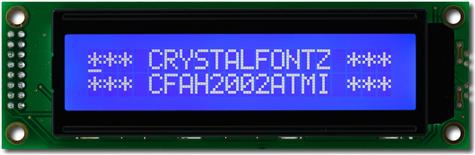
Figure 8.49 Crystalfontz CFAH2002A-TMI 20 × 2 character LCD
© 2012 Crystalfontz America; reprinted with permission.
Figure 8.50 shows the LCD connected to a PIC32 over an 8-bit parallel interface. The logic operates at 5 V but is compatible with 3.3 V inputs from the PIC32. The LCD contrast is set by a second voltage produced with a potentiometer; it is usually most readable at a setting of 4.2–4.8 V. The LCD receives three control signals: RS (1 for characters, 0 for instructions), ![]() (1 to read from the display, 0 to write), and E (pulsed high for at least 250 ns to enable the LCD when the next byte is ready). When the instruction is read, bit 7 returns the busy flag, indicating 1 when busy and 0 when the LCD is ready to accept another instruction. However, certain initialization steps and the clear instruction require a specified delay instead of checking the busy flag.
(1 to read from the display, 0 to write), and E (pulsed high for at least 250 ns to enable the LCD when the next byte is ready). When the instruction is read, bit 7 returns the busy flag, indicating 1 when busy and 0 when the LCD is ready to accept another instruction. However, certain initialization steps and the clear instruction require a specified delay instead of checking the busy flag.
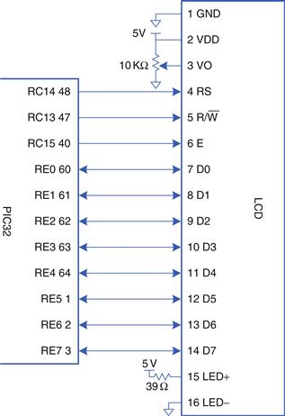
Figure 8.50 Parallel LCD interface
To initialize the LCD, the PIC32 must write a sequence of instructions to the LCD as shown below:
![]() Wait > 15000 μs after VDD is applied
Wait > 15000 μs after VDD is applied
![]() Write 0x30 to set 8-bit mode again
Write 0x30 to set 8-bit mode again
![]() Write 0x30 to set 8-bit mode yet again
Write 0x30 to set 8-bit mode yet again
![]() Write 0x3C to set 2 lines and 5 × 8 dot font
Write 0x3C to set 2 lines and 5 × 8 dot font
![]() Write 0x08 to turn display OFF
Write 0x08 to turn display OFF
![]() Write 0x01 to clear the display
Write 0x01 to clear the display
![]() Write 0x06 to set entry mode to increment cursor after each character
Write 0x06 to set entry mode to increment cursor after each character
Then, to write text to the LCD, the microcontroller can send a sequence of ASCII characters. It may also send the instructions 0x01 to clear the display or 0x02 to return to the home position in the upper left.
Example 8.26 LCD Control
Write a program to write “I love LCDs” to a character display.
Solution
The following program writes “I love LCDs” to the display. It requires the delaymicros function from Example 8.21.
#include <P32xxxx.h>
typedef enum {INSTR, DATA} mode;
char lcdread(mode md) {
char c;
TRISE = 0xFFFF; // make PORTE[7:0] input
PORTCbits.RC14 = (md == DATA); // set instruction or data mode
PORTCbits.RC13 = 1; // read mode
PORTCbits.RC15 = 1; // pulse enable
delaymicros(10); // wait for LCD to respond
c = PORTE & 0x00FF; // read a byte from port E
PORTCbits.RC15 = 0; // turn off enable
delaymicros(10); // wait for LCD to respond
}
void lcdbusywait(void)
{
char state;
do {
state = lcdread(INSTR); // read instruction
} while (state & 0x80); // repeat until busy flag is clear
}
char lcdwrite(char val, mode md) {
TRISE = 0xFF00; // make PORTE[7:0] output
PORTCbits.RC14 = (md == DATA); // set instruction or data mode
PORTCbits.RC13 = 0; // write mode
PORTE = val; // value to write
PORTCbits.RC15 = 1; // pulse enable
delaymicros(10); // wait for LCD to respond
PORTCbits.RC15 = 0; // turn off enable
delaymicros(10); // wait for LCD to respond
}
char lcdprintstring(char *str)
{
while(*str != 0) { // loop until null terminator
lcdwrite(*str, DATA); // print this character
lcdbusywait();
str++; // advance pointer to next character in string
}
}
void lcdclear(void)
{
lcdwrite(0x01, INSTR); // clear display
delaymicros(1530); // wait for execution
}
void initlcd(void) {
// set LCD control pins
TRISC = 0x1FFF; // PORTC[15:13] are outputs, others are inputs
PORTC = 0x0000; // turn off all controls
// send instructions to initialize the display
delaymicros(15000);
lcdwrite(0x30, INSTR); // 8-bit mode
delaymicros(4100);
lcdwrite(0x30, INSTR); // 8-bit mode
delaymicros(100);
lcdwrite(0x30, INSTR); // 8-bit mode yet again!
lcdbusywait();
lcdwrite(0x3C, INSTR); // set 2 lines, 5x8 font
lcdbusywait();
lcdwrite(0x08, INSTR); // turn display off
lcdbusywait();
lcdclear();
lcdwrite(0x06, INSTR); // set entry mode to increment cursor
lcdbusywait();
lcdwrite(0x0C, INSTR); // turn display on with no cursor
lcdbusywait();
}
int main(void) {
initlcd();
lcdprintstring("I love LCDs");
}
VGA Monitor
A more flexible display option is to drive a computer monitor. The Video Graphics Array (VGA) monitor standard was introduced in 1987 for the IBM PS/2 computers, with a 640 × 480 pixel resolution on a cathode ray tube (CRT) and a 15-pin connector conveying color information with analog voltages. Modern LCD monitors have higher resolution but remain backward compatible with the VGA standard.
In a cathode ray tube, an electron gun scans across the screen from left to right exciting fluorescent material to display an image. Color CRTs use three different phosphors for red, green, and blue, and three electron beams. The strength of each beam determines the intensity of each color in the pixel. At the end of each scanline, the gun must turn off for a horizontal blanking interval to return to the beginning of the next line. After all of the scanlines are complete, the gun must turn off again for a vertical blanking interval to return to the upper left corner. The process repeats about 60–75 times per second to give the visual illusion of a steady image.
In a 640 × 480 pixel VGA monitor refreshed at 59.94 Hz, the pixel clock operates at 25.175 MHz, so each pixel is 39.72 ns wide. The full screen can be viewed as 525 horizontal scanlines of 800 pixels each, but only 480 of the scanlines and 640 pixels per scan line actually convey the image, while the remainder are black. A scanline begins with a back porch, the blank section on the left edge of the screen. It then contains 640 pixels, followed by a blank front porch at the right edge of the screen and a horizontal sync (hsync) pulse to rapidly move the gun back to the left edge. Figure 8.51(a) shows the timing of each of these portions of the scanline, beginning with the active pixels. The entire scan line is 31.778 μs long. In the vertical direction, the screen starts with a back porch at the top, followed by 480 active scan lines, followed by a front porch at the bottom and a vertical sync (vsync) pulse to return to the top to start the next frame. A new frame is drawn 60 times per second. Figure 8.51(b) shows the vertical timing; note that the time units are now scan lines rather than pixel clocks. Higher resolutions use a faster pixel clock, up to 388 MHz at 2048 × 1536 @ 85 Hz. For example, 1024 × 768 @ 60 Hz can be achieved with a 65 MHz pixel clock. The horizontal timing involves a front porch of 24 clocks, hsync pulse of 136 clocks, and back porch of 160 clocks. The vertical timing involves a front porch of 3 scan lines, vsync pulse of 6 lines, and back porch of 29 lines.
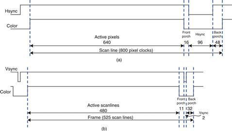
Figure 8.51 VGA timing: (a) horizontal, (b) vertical
Figure 8.52 shows the pinout for a female connector coming from a video source. Pixel information is conveyed with three analog voltages for red, green, and blue. Each voltage ranges from 0–0.7 V, with more positive indicating brighter. The voltages should be 0 during the front and back porches. The cable can also provide an I2C serial link to configure the monitor.
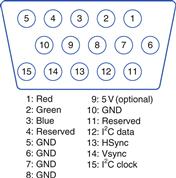
Figure 8.52 VGA connector pinout
The video signal must be generated in real time at high speed, which is difficult on a microcontroller but easy on an FPGA. A simple black and white display could be produced by driving all three color pins with either 0 or 0.7 V using a voltage divider connected to a digital output pin. A color monitor, on the other hand, uses a video DAC with three separate D/A converters to independently drive the three color pins. Figure 8.53 shows an FPGA driving a VGA monitor through an ADV7125 triple 8-bit video DAC. The DAC receives 8 bits of R, G, and B from the FPGA. It also receives a SYNC_b signal that is driven active low whenever HSYNC or VSYNC are asserted. The video DAC produces three output currents to drive the red, green, and blue analog lines, which are normally 75 Ω transmission lines parallel terminated at both the video DAC and the monitor. The RSET resistor sets the scale of the output current to achieve the full range of color. The clock rate depends on the resolution and refresh rate; it may be as high as 330 MHz with a fast-grade ADV7125JSTZ330 model DAC.
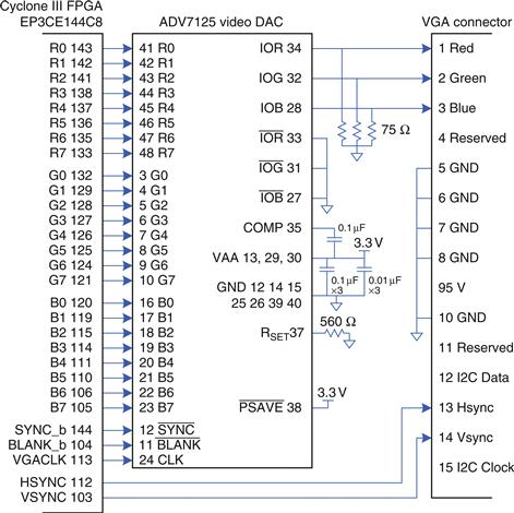
Figure 8.53 FPGA driving VGA cable through video DAC
Example 8.27 VGA Monitor Display
Write HDL code to display text and a green box on a VGA monitor using the circuitry from Figure 8.53.
Solution
The code assumes a system clock frequency of 40 MHz and uses a phase-locked loop (PLL) on the FPGA to generate the 25.175 MHz VGA clock. PLL configuration varies among FPGAs; for the Cyclone III, the frequencies are specified with Altera’s megafunction wizard. Alternatively, the VGA clock could be provided directly from a signal generator.
The VGA controller counts through the columns and rows of the screen, generating the hsync and vsync signals at the appropriate times. It also produces a blank_b signal that is asserted low to draw black when the coordinates are outside the 640 × 480 active region.
The video generator produces red, green, and blue color values based on the current (x, y) pixel location. (0, 0) represents the upper left corner. The generator draws a set of characters on the screen, along with a green rectangle. The character generator draws an 8 × 8-pixel character, giving a screen size of 80 × 60 characters. It looks up the character from a ROM, where it is encoded in binary as 6 columns by 8 rows. The other two columns are blank. The bit order is reversed by the SystemVerilog code because the leftmost column in the ROM file is the most significant bit, while it should be drawn in the least significant x-position.
Figure 8.54 shows a photograph of the VGA monitor while running this program. The rows of letters alternate red and blue. A green box overlays part of the image.

Figure 8.54 VGA output
vga.sv
module vga(input logic clk,
output logic vgaclk, // 25.175 MHz VGA clock
output logic hsync, vsync,
output logic sync_b, blank_b, // to monitor & DAC
output logic [7:0] r, g, b); // to video DAC
logic [9:0] x, y;
// Use a PLL to create the 25.175 MHz VGA pixel clock
// 25.175 MHz clk period = 39.772 ns
// Screen is 800 clocks wide by 525 tall, but only 640 x 480 used for display
// HSync = 1/(39.772 ns * 800) = 31.470 KHz
// Vsync = 31.474 KHz / 525 = 59.94 Hz (~60 Hz refresh rate)
pll vgapll(.inclk0(clk), .c0(vgaclk));
// generate monitor timing signals
vgaController vgaCont(vgaclk, hsync, vsync, sync_b, blank_b, x, y);
// user-defined module to determine pixel color
videoGen videoGen(x, y, r, g, b);
endmodule
module vgaController #(parameter HACTIVE = 10’d640,
HFP = 10’d16,
HSYN = 10’d96,
HBP = 10’d48,
HMAX = HACTIVE + HFP + HSYN + HBP,
VBP = 10’d32,
VACTIVE = 10’d480,
VFP = 10’d11,
VSYN = 10’d2,
VMAX = VACTIVE + VFP + VSYN + VBP)
(input logic vgaclk,
output logic hsync, vsync, sync_b, blank_b,
output logic [9:0] x, y);
// counters for horizontal and vertical positions
always @(posedge vgaclk) begin
x++;
if (x == HMAX) begin
x = 0;
y++;
if (y == VMAX) y = 0;
end
end
// compute sync signals (active low)
assign hsync = ~(hcnt >= HACTIVE + HFP & hcnt < HACTIVE + HFP + HSYN);
assign vsync = ~(vcnt >= VACTIVE + VFP & vcnt < VACTIVE + VFP + VSYN);
assign sync_b = hsync & vsync;
// force outputs to black when outside the legal display area
assign blank_b = (hcnt < HACTIVE) & (vcnt < VACTIVE);
endmodule
module videoGen(input logic [9:0] x, y, output logic [7:0] r, g, b);
logic pixel, inrect;
// given y position, choose a character to display
// then look up the pixel value from the character ROM
// and display it in red or blue. Also draw a green rectangle.
chargenrom chargenromb(y[8:3]+8’d65, x[2:0], y[2:0], pixel);
rectgen rectgen(x, y, 10’d120, 10’d150, 10’d200, 10’d230, inrect);
assign {r, b} = (y[3]==0) ? {{8{pixel}},8’h00} : {8’h00,{8{pixel}}};
assign g = inrect ? 8’hFF : 8’h00;
endmodule
module chargenrom(input logic [7:0] ch,
input logic [2:0] xoff, yoff,
output logic pixel);
logic [5:0] charrom[2047:0]; // character generator ROM
logic [7:0] line; // a line read from the ROM
// initialize ROM with characters from text file
initial
$readmemb("charrom.txt", charrom);
// index into ROM to find line of character
assign line = charrom[yoff+{ch-65, 3’b000}]; // subtract 65 because A
// is entry 0
// reverse order of bits
assign pixel = line[3’d7-xoff];
endmodule
module rectgen(input logic [9:0] x, y, left, top, right, bot,
output logic inrect);
assign inrect = (x >= left & x < right & y >= top & y < bot);
endmodule
charrom.txt
// A ASCII 65
011100
100010
100010
111110
100010
100010
100010
000000
//B ASCII 66
111100
100010
100010
111100
100010
100010
111100
000000
//C ASCII 67
011100
100010
100000
100000
100000
100010
011100
000000
...
Bluetooth Wireless Communication
There are many standards now available for wireless communication, including Wi-Fi, ZigBee, and Bluetooth. The standards are elaborate and require sophisticated integrated circuits, but a growing assortment of modules abstract away the complexity and give the user a simple interface for wireless communication. One of these modules is the BlueSMiRF, which is an easy-to-use Bluetooth wireless interface that can be used instead of a serial cable.
Bluetooth is a wireless standard developed by Ericsson in 1994 for low-power, moderate speed, communication over distances of 5–100 meters, depending on the transmitter power level. It is commonly used to connect an earpiece to a cellphone or a keyboard to a computer. Unlike infrared communication links, it does not require a direct line of sight between devices.
Bluetooth is named for King Harald Bluetooth of Denmark, a 10th century monarch who unified the warring Danish tribes. This wireless standard was only partially successful at unifying a host of competing wireless protocols!
Bluetooth operates in the 2.4 GHz unlicensed industrial-scientific-medical (ISM) band. It defines 79 radio channels spaced at 1 MHz intervals starting at 2402 MHz. It hops between these channels in a pseudo-random pattern to avoid consistent interference with other devices like wireless phones operating in the same band. As given in Table 8.10, Bluetooth transmitters are classified at one of three power levels, which dictate the range and power consumption. In the basic rate mode, it operates at 1 Mbit/sec using Gaussian frequency shift keying (FSK). In ordinary FSK, each bit is conveyed by transmitting a frequency of fc ± fd, where fc is the center frequency of the channel and fd is an offset of at least 115 kHz. The abrupt transition in frequencies between bits consumes extra bandwidth. In Gaussian FSK, the change in frequency is smoothed to make better use of the spectrum. Figure 8.55 shows the frequencies being transmitted for a sequence of 0’s and 1’s on a 2402 MHz channel using FSK and GFSK.
Table 8.10 Bluetooth classes
| Class | Transmitter Power (mW) | Range (m) |
| 1 | 100 | 100 |
| 2 | 2.5 | 10 |
| 3 | 1 | 5 |

Figure 8.55 FSK and GFSK waveforms
A BlueSMiRF Silver module, shown in Figure 8.56, contains a Class 2 Bluetooth radio, modem, and interface circuitry on a small card with a serial interface. It communicates with another Bluetooth device such as a Bluetooth USB dongle connected to a PC. Thus, it can provide a wireless serial link between a PIC32 and a PC similar to the link from Figure 8.43 but without the cable. Figure 8.57 shows a schematic for such a link. The TX pin of the BlueSMiRF connects to the RX pin of the PIC32, and vice versa. The RTS and CTS pins are connected so that the BlueSMiRF shakes its own hand.

Figure 8.56 BlueSMiRF module and USB dongle
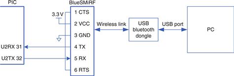
Figure 8.57 Bluetooth PIC32 to PC link
The BlueSMiRF defaults to 115.2k baud with 8 data bits, 1 stop bit, and no parity or flow control. It operates at 3.3 V digital logic levels, so no RS-232 transceiver is necessary to connect with another 3.3 V device.
To use the interface, plug a USB Bluetooth dongle into a PC. Power up the PIC32 and BlueSMiRF. The red STAT light will flash on the BlueSMiRF indicating that it is waiting to make a connection. Open the Bluetooth icon in the PC system tray and use the Add Bluetooth Device Wizard to pair the dongle with the BlueSMiRF. The default passkey for the BlueSMiRF is 1234. Take note of which COM port is assigned to the dongle. Then communication can proceed just as it would over a serial cable. Note that the dongle typically operates at 9600 baud and that PuTTY must be configured accordingly.
Motor Control
Another major application of microcontrollers is to drive actuators such as motors. This section describes three types of motors: DC motors, servo motors, and stepper motors. DC motors require a high drive current, so a powerful driver such as an H-bridge must be connected between the microcontroller and the motor. They also require a separate shaft encoder if the user wants to know the current position of the motor. Servo motors accept a pulse-width modulated signal to specify their position over a limited range of angles. They are very easy to interface, but are not as powerful and are not suited to continuous rotation. Stepper motors accept a sequence of pulses, each of which rotates the motor by a fixed angle called a step. They are more expensive and still need an H-bridge to drive the high current, but the position can be precisely controlled.
Motors can draw a substantial amount of current and may introduce glitches on the power supply that disturb digital logic. One way to reduce this problem is to use a different power supply or battery for the motor than for the digital logic.
DC Motors
Figure 8.58 shows the operation of a brushed DC motor. The motor is a two terminal device. It contains permanent stationary magnets called the stator and a rotating electromagnet called the rotor or armature connected to the shaft. The front end of the rotor connects to a split metal ring called a commutator. Metal brushes attached to the power lugs (input terminals) rub against the commutator, providing current to the rotor’s electromagnet. This induces a magnetic field in the rotor that causes the rotor to spin to become aligned with the stator field. Once the rotor has spun part way around and approaches alignment with the stator, the brushes touch the opposite sides of the commutator, reversing the current flow and magnetic field and causing it to continue spinning indefinitely.
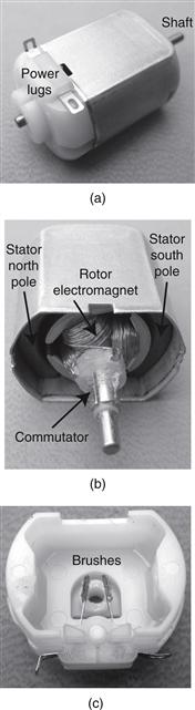
Figure 8.58 DC motor
DC motors tend to spin at thousands of rotations per minute (RPM) at very low torque. Most systems add a gear train to reduce the speed to a more reasonable level and increase the torque. Look for a gear train designed to mate with your motor. Pittman manufactures a wide range of high quality DC motors and accessories, while inexpensive toy motors are popular among hobbyists.
A DC motor requires substantial current and voltage to deliver significant power to a load. The current should be reversible if the motor can spin in both directions. Most microcontrollers cannot produce enough current to drive a DC motor directly. Instead, they use an H-bridge, which conceptually contains four electrically controlled switches, as shown in Figure 8.59(a). If switches A and D are closed, current flows from left to right through the motor and it spins in one direction. If B and C are closed, current flows from right to left through the motor and it spins in the other direction. If A and C or B and D are closed, the voltage across the motor is forced to 0, causing the motor to actively brake. If none of the switches are closed, the motor will coast to a stop. The switches in an H-bridge are power transistors. The H-bridge also contains some digital logic to conveniently control the switches. When the motor current changes abruptly, the inductance of the motor’s electromagnet will induce a large voltage that could exceed the power supply and damage the power transistors. Therefore, many H-bridges also have protection diodes in parallel with the switches, as shown in Figure 8.59(b). If the inductive kick drives either terminal of the motor above Vmotor or below ground, the diodes will turn ON and clamp the voltage at a safe level. H-bridges can dissipate large amounts of power, and a heat sink may be necessary to keep them cool.
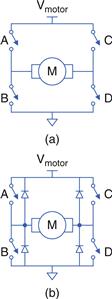
Figure 8.59 H-bridge
Example 8.28 Autonomous Vehicle
Design a system in which a PIC32 controls two drive motors for a robot car. Write a library of functions to initialize the motor driver and to make the car drive forward and back, turn left or right, and stop. Use PWM to control the speed of the motors.
Solution
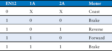
Figure 8.60 shows a pair of DC motors controlled by a PIC32 using a Texas Instruments SN754410 dual H-bridge. The H-bridge requires a 5 V logic supply VCC1 and a 4.5-36 V motor supply VCC2; it has VIH = 2 V and is hence compatible with the 3.3 V I/O from the PIC32. It can deliver up to 1 A of current to each of two motors. Table 8.11 describes how the inputs to each H-bridge control a motor. The microcontroller drives the enable signals with a PWM signal to control the speed of the motors. It drives the four other pins to control the direction of each motor.
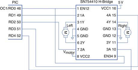
Figure 8.60 Motor control with dual H-bridge
Table 8.11 H-Bridge control
The PWM is configured to work at about 781 Hz with a duty cycle ranging from 0 to 100%.
#include <P32xxxx.h>
void setspeed(int dutycycle) {
OC1RS = dutycycle; // set duty cycle between 0 and 100
}
void setmotorleft(int dir) { // dir of 1 = forward, 0 = backward
PORTDbits.RD1 = dir; PORTDbits.RD2 = !dir;
}
void setmotorright(int dir) { // dir of 1 = forward, 0 = backward
PORTDbits.RD3 = dir; PORTDbits.RD4 = !dir;
}
void forward(void) {
setmotorleft(1); setmotorright(1); // both motors drive forward
}
void backward(void) {
setmotorleft(0); setmotorright(0); // both motors drive backward
}
void left(void) {
setmotorleft(0); setmotorright(1); // left back, right forward
}
void right(void) {
setmotorleft(1); setmotorright(0); // right back, left forward
}
void halt(void) {
PORTDCLR = 0x001E; // turn both motors off by
// clearing RD[4:1] to 0
}
void initmotors(void) {
TRISD = 0xFFE0; // RD[4:0] are outputs
halt(); // ensure motors aren’t spinning
// configure PWM on OC1 (RD0)
T2CONbits.TCKPS = 0b111; // prescale by 256 to 78.125 KHz
PR2 = 99; // set period to 99+1 ticks = 781.25 Hz
OC1RS = 0; // start with low H-bridge enable signal
OC1CONbits.OCM = 0b110; // set output compare 1 module to PWM mode
T2CONbits.ON = 1; // turn on timer 2
OC1CONbits.ON = 1; // turn on PWM
}
In the previous example, there is no way to measure the position of each motor. Two motors are unlikely to be exactly matched, so one is likely to turn slightly faster than the other, causing the robot to veer off course. To solve this problem, some systems add shaft encoders. Figure 8.61(a) shows a simple shaft encoder consisting of a disk with slots attached to the motor shaft. An LED is placed on one side and a light sensor is placed on the other side. The shaft encoder produces a pulse every time the gap rotates past the LED. A microcontroller can count these pulses to measure the total angle that the shaft has turned. By using two LED/sensor pairs spaced half a slot width apart, an improved shaft encoder can produce quadrature outputs shown in Figure 8.61(b) that indicate the direction the shaft is turning as well as the angle by which it has turned. Sometimes shaft encoders add another hole to indicate when the shaft is at an index position.
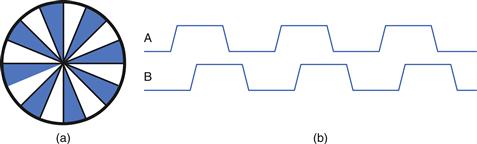
Figure 8.61 Shaft encoder (a) disk, (b) quadrature outputs
Servo Motor
A servo motor is a DC motor integrated with a gear train, a shaft encoder, and some control logic so that it is easier to use. They have a limited rotation, typically 180°. Figure 8.62 shows a servo with the lid removed to reveal the gears. A servo motor has a 3-pin interface with power (typically 5 V), ground, and a control input. The control input is typically a 50 Hz pulse-width modulated signal. The servo’s control logic drives the shaft to a position determined by the duty cycle of the control input. The servo’s shaft encoder is typically a rotary potentiometer that produces a voltage dependent on the shaft position.

Figure 8.62 SG90 servo motor
In a typical servo motor with 180 degrees of rotation, a pulse width of 0.5 ms drives the shaft to 0°, 1.5 ms to 90°, and 2.5 ms to 180°. For example, Figure 8.63 shows a control signal with a 1.5 ms pulse width. Driving the servo outside its range may cause it to hit mechanical stops and be damaged. The servo’s power comes from the power pin rather than the control pin, so the control can connect directly to a microcontroller without an H-bridge. Servo motors are commonly used in remote-control model airplanes and small robots because they are small, light, and convenient. Finding a motor with an adequate datasheet can be difficult. The center pin with a red wire is normally power, and the black or brown wire is normally ground.
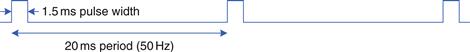
Figure 8.63 Servo control waveform
Example 8.29 Servo Motor
Design a system in which a PIC32 microcontroller drives a servo motor to a desired angle.
Solution
Figure 8.64 shows a diagram of the connection to an SG90 servo motor. The servo operates off of a 4.0–7.2 V power supply. Only a single wire is necessary to carry the PWM signal, which can be provided at 5 or 3.3 V logic levels. The code configures the PWM generation using the Output Compare 1 module and sets the appropriate duty cycle for the desired angle.
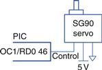
Figure 8.64 Servo motor control
#include <P32xxxx.h>
void initservo(void) { // configure PWM on OC1 (RD0)
T2CONbits.TCKPS = 0b111; // prescale by 256 to 78.125 KHz
PR2 = 1561; // set period to 1562 ticks = 50.016 Hz (20 ms)
OC1RS = 117; // set pulse width to 1.5 ms to center servo
OC1CONbits.OCM = 0b110; // set output compare 1 module to PWM mode
T2CONbits.ON = 1; // turn on timer 2
OC1CONbits.ON = 1; // turn on PWM
}
void setservo(int angle) {
if (angle < 0) angle = 0; // angle must be in the range of
// 0-180 degrees
else if (angle > 180) angle = 180;
OC1RS = 39+angle*156.1/180; // set pulsewidth of 39-195 ticks //
(0.5-2.5 ms) based on angle
}
It is also possible to convert an ordinary servo into a continuous rotation servo by carefully disassembling it, removing the mechanical stop, and replacing the potentiometer with a fixed voltage divider. Many websites show detailed directions for particular servos. The PWM will then control the velocity rather than position, with 1.5 ms indicating stop, 2.5 ms indicating full speed forward, and 0.5 ms indicating full speed backward. A continuous rotation servo may be more convenient and less expensive than a simple DC motor combined with an H-bridge and gear train.
Stepper Motor
A stepper motor advances in discrete steps as pulses are applied to alternate inputs. The step size is usually a few degrees, allowing precise positioning and continuous rotation. Small stepper motors generally come with two sets of coils called phases wired in bipolar or unipolar fashion. Bipolar motors are more powerful and less expensive for a given size but require an H-bridge driver, while unipolar motors can be driven with transistors acting as switches. This section focuses on the more efficient bipolar stepper motor.
Figure 8.65(a) shows a simplified two-phase bipolar motor with a 90° step size. The rotor is a permanent magnet with one north and one south pole. The stator is an electromagnet with two pairs of coils comprising the two phases. Two-phase bipolar motors thus have four terminals. Figure 8.65(b) shows a symbol for the stepper motor modeling the two coils as inductors.
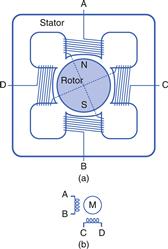
Figure 8.65 (a) Simplified bipolar stepper motor; (b) stepper motor symbol
Figure 8.66 shows three common drive sequences for a two phase bipolar motor. Figure 8.66(a) illustrates wave drive, in which the coils are energized in the sequence AB – CD – BA – DC. Note that BA means that the winding AB is energized with current flowing in the opposite direction; this is the origin of the name bipolar. The rotor turns by 90 degrees at each step. Figure 8.66(b) illustrates two-phase-on drive, following the pattern (AB, CD) – (BA, CD) – (BA, DC) – (AB, DC). (AB, CD) indicates that both coils AB and CD are energized simultaneously. The rotor again turns by 90 degrees at each step, but aligns itself halfway between the two pole positions. This gives the highest torque operation because both coils are delivering power at once. Figure 8.66(c) illustrates half-step drive, following the pattern (AB, CD) – CD – (BA, CD) – BA – (BA, DC) – DC – (AB, DC) – AB. The rotor turns by 45 degrees at each half-step. The rate at which the pattern advances determines the speed of the motor. To reverse the motor direction, the same drive sequences are applied in the opposite order.
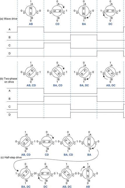
Figure 8.66 Bipolar motor drive
In a real motor, the rotor has many poles to make the angle between steps much smaller. For example, Figure 8.67 shows an AIRPAX LB82773-M1 bipolar stepper motor with a 7.5 degree step size. The motor operates off 5 V and draws 0.8 A through each coil.

Figure 8.67 AIRPAX LB82773-M1 bipolar stepper motor
The torque in the motor is proportional to the coil current. This current is determined by the voltage applied and by the inductance L and resistance R of the coil. The simplest mode of operation is called direct voltage drive or L/R drive, in which the voltage V is directly applied to the coil. The current ramps up to I = V/R with a time constant set by L/R, as shown in Figure 8.68(a). This works well for slow speed operation. However, at higher speed, the current doesn’t have enough time to ramp up to the full level, as shown in Figure 8.68(b), and the torque drops off.
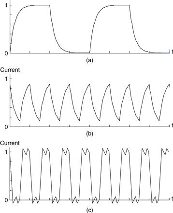
Figure 8.68 Bipolar stepper motor direct drive current: (a) slow rotation, (b) fast rotation, (c) fast rotation with chopper drive
A more efficient way to drive a stepper motor is by pulse-width modulating a higher voltage. The high voltage causes the current to ramp up to full current more rapidly, then it is turned off (PWM) to avoid overloading the motor. The voltage is then modulated or chopped to maintain the current near the desired level. This is called chopper constant current drive and is shown in Figure 8.68(c). The controller uses a small resistor in series with the motor to sense the current being applied by measuring the voltage drop, and applies an enable signal to the H-bridge to turn off the drive when the current reaches the desired level. In principle, a microcontroller could generate the right waveforms, but it is easier to use a stepper motor controller. The L297 controller from ST Microelectronics is a convenient choice, especially when coupled with the L298 dual H-bridge with current sensing pins and a 2 A peak power capability. Unfortunately, the L298 is not available in a DIP package so it is harder to breadboard. ST’s application notes AN460 and AN470 are valuable references for stepper motor designers.
Example 8.30 Bipolar Stepper Motor Direct Wave Drive
Design a system in which a PIC32 microcontroller drives an AIRPAX bipolar stepper motor at a specified speed and direction using direct drive.
Solution
Figure 8.69 shows a bipolar stepper motor being driven directly by an H-bridge controlled by a PIC32.

Figure 8.69 Bipolar stepper motor direct drive with H-bridge
The spinstepper function initializes the sequence array with the patterns to apply to RD[4:0] to follow the direct drive sequence. It applies the next pattern in the sequence, then waits a sufficient time to rotate at the desired revolutions per minute (RPM). Using a 20 MHz clock and a 7.5° step size with a 16-bit timer and 256:1 prescalar, the feasible range of speeds is 2–230 rpm, with the bottom end limited by the timer resolution and the top end limited by the power of the LB82773-M1 motor.
#include <P32xxxx.h>
#define STEPSIZE 7.5 // size of step, in degrees
int curstepstate; // keep track of current state of stepper motor in sequence
void initstepper(void) {
TRISD = 0xFFE0; // RD[4:0] are outputs
curstepstate = 0;
T1CONbits.ON = 0; // turn Timer1 off
T1CONbits.TCKPS = 3; // prescale by 256 to run slower
}
void spinstepper(int dir, int steps, float rpm) { // dir = 0 for forward, 1 = reverse
{
int sequence[4] = {0b00011, 0b01001, 0b00101, 0b10001}; // wave drive sequence
int step;
PR1 = (int)(20.0e6/(256*(360.0/STEPSIZE)*(rpm/60.0))); // time/step w/ 20 MHz peripheral clock
TMR1 = 0;
T1CONbits.ON = 1; // turn Timer1 on
for (step = 0; step < steps; step++) { // take specified number of steps
PORTD = sequence[curstepstate]; // apply current step control
if (dir == 0) curstepstate = (curstepstate + 1) % 4; // determine next state forward
else curstepstate = (curstepstate + 3) % 4; // determine next state backward
while (!IFS0bits.T1IF); // wait for timer to overflow
IFS0bits.T1IF = 0; // clear overflow flag
}
T1CONbits.ON = 0; // Timer1 off to save power when done
}
8.7 PC I/O Systems
Personal computers (PCs) use a wide variety of I/O protocols for purposes including memory, disks, networking, internal expansion cards, and external devices. These I/O standards have evolved to offer very high performance and to make it easy for users to add devices. These attributes come at the expense of complexity in the I/O protocols. This section explores the major I/O standards used in PCs and examines some options for connecting a PC to custom digital logic or other external hardware.
Figure 8.70 shows a PC motherboard for a Core i5 or i7 processor. The processor is packaged in a land grid array with 1156 gold-plated pads to supply power and ground to the processor and connect the processor to memory and I/O devices. The motherboard contains the DRAM memory module slots, a wide variety of I/O device connectors, and the power supply connector, voltage regulators, and capacitors. A pair of DRAM modules are connected over a DDR3 interface. External peripherals such as keyboards or webcams are attached over USB. High-performance expansion cards such as graphics cards connect over the PCI Express x16 slot, while lower-performance cards can use PCI Express x1 or the older PCI slots. The PC connects to the network using the Ethernet jack. The hard disk connects to a SATA port. The remainder of this section gives an overview of the operation of each of these I/O standards.
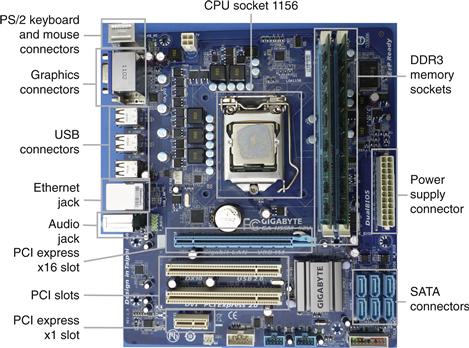
Figure 8.70 Gigabyte GA-H55M-S2V Motherboard
One of the major advances in PC I/O standards has been the development of high-speed serial links. Until recently, most I/O was built around parallel links consisting of a wide data bus and a clock signal. As data rates increased, the difference in delay among the wires in the bus set a limit to how fast the bus could run. Moreover, busses connected to multiple devices suffer from transmission line problems such as reflections and different flight times to different loads. Noise can also corrupt the data. Point-to-point serial links eliminate many of these problems. The data is usually transmitted on a differential pair of wires. External noise that affects both wires in the pair equally is unimportant. The transmission lines are easy to properly terminate, so reflections are small (see Section A.8 on transmission lines). No explicit clock is sent; instead, the clock is recovered at the receiver by watching the timing of the data transitions. High-speed serial link design is a specialized subject, but good interfaces can run faster than 10 Gb/s over copper wires and even faster along optical fibers.
8.7.1 USB
Until the mid-1990’s, adding a peripheral to a PC took some technical savvy. Adding expansion cards required opening the case, setting jumpers to the correct position, and manually installing a device driver. Adding an RS-232 device required choosing the right cable and properly configuring the baud rate, and data, parity, and stop bits. The Universal Serial Bus (USB), developed by Intel, IBM, Microsoft, and others, greatly simplified adding peripherals by standardizing the cables and software configuration process. Billions of USB peripherals are now sold each year.
USB 1.0 was released in 1996. It uses a simple cable with four wires: 5 V, GND, and a differential pair of wires to carry data. The cable is impossible to plug in backward or upside down. It operates at up to 12 Mb/s. A device can pull up to 500 mA from the USB port, so keyboards, mice, and other peripherals can get their power from the port rather than from batteries or a separate power cable.
USB 2.0, released in 2000, upgraded the speed to 480 Mb/s by running the differential wires much faster. With the faster link, USB became practical for attaching webcams and external hard disks. Flash memory sticks with a USB interface also replaced floppy disks as a means of transferring files between computers.
USB 3.0, released in 2008, further boosted the speed to 5 Gb/s. It uses the same shape connector, but the cable has more wires that operate at very high speed. It is better suited to connecting high-performance hard disks. At about the same time, USB added a Battery Charging Specification that boosts the power supplied over the port to speed up charging mobile devices.
The simplicity for the user comes at the expense of a much more complex hardware and software implementation. Building a USB interface from the ground up is a major undertaking. Even writing a simple device driver is moderately complex. The PIC32 comes with a built-in USB controller. However, Microchip’s device driver to connect a mouse to the PIC32 (available at microchip.com) is more than 500 lines of code and is beyond the scope of this chapter.
8.7.2 PCI and PCI Express
The Peripheral Component Interconnect (PCI) bus is an expansion bus standard developed by Intel that became widespread around 1994. It was used to add expansion cards such as extra serial or USB ports, network interfaces, sound cards, modems, disk controllers, or video cards. The 32-bit parallel bus operates at 33 MHz, giving a bandwidth of 133 MB/s.
The demand for PCI expansion cards has steadily declined. More standard ports such as Ethernet and SATA are now integrated into the motherboard. Many devices that once required an expansion card can now be connected over a fast USB 2.0 or 3.0 link. And video cards now require far more bandwidth than PCI can supply.
Contemporary motherboards often still have a small number of PCI slots, but fast devices like video cards are now connected via PCI Express (PCIe). PCI Express slots provide one or more lanes of high-speed serial links. In PCIe 3.0, each lane operates at up to 8 Gb/s. Most motherboards provide an x16 slot with 16 lanes giving a total of 16 GB/s of bandwidth to data-hungry devices such as video cards.
8.7.3 DDR3 Memory
DRAM connects to the microprocessor over a parallel bus. In 2012, the present standard is DDR3, a third generation of double-data rate memory bus operating at 1.5 V. Typical motherboards now come with two DDR3 channels so they can access two banks of memory modules simultaneously.
Figure 8.71 shows a 4 GB DDR3 dual inline memory module (DIMM). The module has 120 contacts on each side, for a total of 240 connections, including a 64-bit data bus, a 16-bit time-multiplexed address bus, control signals, and numerous power and ground pins. In 2012, DIMMs typically carry 1–16 GB of DRAM. Memory capacity has been doubling approximately every 2–3 years.
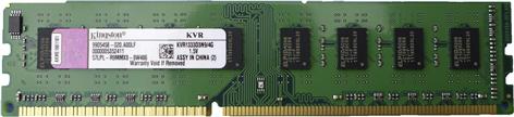
Figure 8.71 DDR3 memory module
DRAM presently operates at a clock rate of 100–266 MHz. DDR3 operates the memory bus at four times the DRAM clock rate. Moreover, it transfers data on both the rising and falling edges of the clock. Hence, it sends 8 words of data for each memory clock. At 64 bits/word, this corresponds to 6.4–17 GB/s of bandwidth. For example, DDR3-1600 uses a 200 MHz memory clock and an 800 MHz I/O clock to send 1600 million words/sec, or 12800 MB/s. Hence, the modules are also called PC3-12800. Unfortunately, DRAM latency remains high, with a roughly 50 ns lag from a read request until the arrival of the first word of data.
8.7.4 Networking
Computers connect to the Internet over a network interface running the Transmission Control Protocol and Internet Protocol (TCP/IP). The physical connection may be an Ethernet cable or a wireless Wi-Fi link.
Ethernet is defined by the IEEE 802.3 standard. It was developed at Xerox Palo Alto Research Center (PARC) in 1974. It originally operated at 10 Mb/s (called 10 Mbit Ethernet), but now is commonly found at 100 Mbit (Mb/s) and 1 Gbit (Gb/s) running on Category 5 cables containing four twisted pairs of wires. 10 Gbit Ethernet running on fiber optic cables is increasingly popular for servers and other high-performance computing, and 100 Gbit Ethernet is emerging.
Wi-Fi is the popular name for the IEEE 802.11 wireless network standard. It operates in the 2.4 and 5 GHz unlicensed wireless bands, meaning that the user doesn’t need a radio operator’s license to transmit in these bands at low power. Table 8.12 summarizes the capabilities of three generations of Wi-Fi; the emerging 802.11ac standard promises to push wireless data rates beyond 1 Gb/s. The increasing performance comes from advancing modulation and signal processing, multiple antennas, and wider signal bandwidths.
Table 8.12 802.11 Wi-Fi Protocols
8.7.5 SATA
Internal hard disks require a fast interface to a PC. In 1986, Western Digital introduced the Integrated Drive Electronics (IDE) interface, which evolved into the AT Attachment (ATA) standard. The standard uses a bulky 40 or 80-wire ribbon cable with a maximum length of 18” to send data at 16–133 MB/s.
ATA has been supplanted by Serial ATA (SATA), which uses high-speed serial links to run at 1.5, 3, or 6 Gb/s over a more convenient 7-conductor cable shown in Figure 8.72. The fastest solid-state drives in 2012 approach 500 MB/s of bandwidth, taking full advantage of SATA.
Figure 8.72 SATA cable
A related standard is Serial Attached SCSI (SAS), an evolution of the parallel SCSI (Small Computer System Interface) interface. SAS offers performance comparable to SATA and supports longer cables; it is common in server computers.
8.7.6 Interfacing to a PC
All of the PC I/O standards described so far are optimized for high performance and ease of attachment but are difficult to implement in hardware. Engineers and scientists often need a way to connect a PC to external circuitry, such as sensors, actuators, microcontrollers, or FPGAs. The serial connection described in Section 8.6.3.2 is sufficient for a low-speed connection to a microcontroller with a UART. This section describes two more means: data acquisition systems, and USB links.
Data Acquisition Systems
Data Acquisition Systems (DAQs) connect a computer to the real world using multiple channels of analog and/or digital I/O. DAQs are now commonly available as USB devices, making them easy to install. National Instruments (NI) is a leading DAQ manufacturer.
High-performance DAQ prices tend to run into the thousands of dollars, mostly because the market is small and has limited competition. Fortunately, as of 2012, NI now sells their handy myDAQ system at a student discount price of $200 including their LabVIEW software. Figure 8.73 shows a myDAQ. It has two analog channels capable of input and output at 200 ksamples/sec with a 16 bit resolution and ±10V dynamic range. These channels can be configured to operate as an oscilloscope and signal generator. It also has eight digital input and output lines compatible with 3.3 and 5 V systems. Moreover, it generates +5, +15, and −15 V power supply outputs and includes a digital multimeter capable of measuring voltage, current, and resistance. Thus, the myDAQ can replace an entire bench of test and measurement equipment while simultaneously offering automated data logging.
Figure 8.73 NI myDAQ
Most NI DAQs are controlled with LabVIEW, NI’s graphical language for designing measurement and control systems. Some DAQs can also be controlled from C programs using the LabWindows environment, from Microsoft .NET applications using the Measurement Studio environment, or from Matlab using the Data Acquisition Toolbox.
USB Links
An increasing variety of products now provide simple, inexpensive digital links between PCs and external hardware over USB. These products contain predeveloped drivers and libraries, allowing the user to easily write a program on the PC that blasts data to and from an FPGA or microcontroller.
FTDI is a leading vendor for such systems. For example, the FTDI C232HM-DDHSL USB to Multi-Protocol Synchronous Serial Engine (MPSSE) cable shown in Figure 8.74 provides a USB jack at one end and, at the other end, an SPI interface operating at up to 30 Mb/s, along with 3.3 V power and four general purpose I/O pins. Figure 8.75 shows an example of connecting a PC to an FPGA using the cable. The cable can optionally supply 3.3 V power to the FPGA. The three SPI pins connect to an FPGA slave device like the one from Example 8.19. The figure also shows one of the GPIO pins used to drive an LED.
Figure 8.74 FTDI USB to MPSSE cable
© 2012 by FTDI; reprinted with permission.
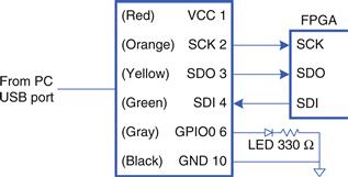
Figure 8.75 C232HM-DDHSL USB to MPSESE interface from PC to FPGA
The PC requires the D2XX dynamically linked library driver to be installed. You can then write a C program using the library to send data over the cable.
If an even faster connection is required, the FTDI UM232H module shown in Figure 8.76 links a PC’s USB port to an 8-bit synchronous parallel interface operating up to 40 MB/s.
Figure 8.76 FTDI UM232H module
© 2012 by FTDI; reprinted with permission.
8.8 Real-World Perspective: x86 Memory and I/O Systems*
As processors get faster, they need ever more elaborate memory hierarchies to keep a steady supply of data and instructions flowing. This section describes the memory systems of x86 processors to illustrate the progression. Section 7.9 contained photographs of the processors, highlighting the on-chip caches. x86 also has an unusual programmed I/O system that differs from the more common memory-mapped I/O.
8.8.1 x86 Cache Systems
The 80386, initially produced in 1985, operated at 16 MHz. It lacked a cache, so it directly accessed main memory for all instructions and data. Depending on the speed of the memory, the processor might get an immediate response, or it might have to pause for one or more cycles for the memory to react. These cycles are called wait states, and they increase the CPI of the processor. Microprocessor clock frequencies have increased by at least 25% per year since then, whereas memory latency has scarcely diminished. The delay from when the processor sends an address to main memory until the memory returns the data can now exceed 100 processor clock cycles. Therefore, caches with a low miss rate are essential to good performance. Table 8.13 summarizes the evolution of cache systems on Intel x86 processors.
Table 8.13 Evolution of Intel x86 microprocessor memory systems
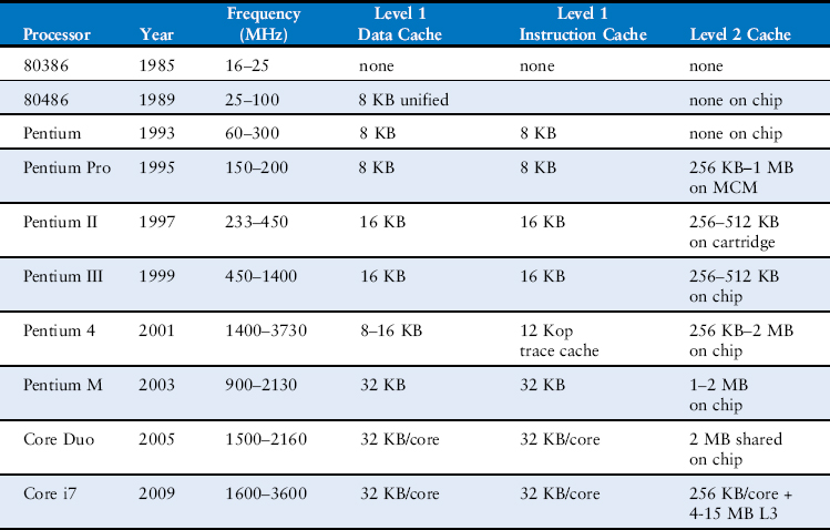
The 80486 introduced a unified write-through cache to hold both instructions and data. Most high-performance computer systems also provided a larger second-level cache on the motherboard using commercially available SRAM chips that were substantially faster than main memory.
The Pentium processor introduced separate instruction and data caches to avoid contention during simultaneous requests for data and instructions. The caches used a write-back policy, reducing the communication with main memory. Again, a larger second-level cache (typically 256–512 KB) was usually offered on the motherboard.
The P6 series of processors (Pentium Pro, Pentium II, and Pentium III) were designed for much higher clock frequencies. The second-level cache on the motherboard could not keep up, so it was moved closer to the processor to improve its latency and throughput. The Pentium Pro was packaged in a multichip module (MCM) containing both the processor chip and a second-level cache chip, as shown in Figure 8.77. Like the Pentium, the processor had separate 8-KB level 1 instruction and data caches. However, these caches were nonblocking, so that the out-of-order processor could continue executing subsequent cache accesses even if the cache missed a particular access and had to fetch data from main memory. The second-level cache was 256 KB, 512 KB, or 1 MB in size and could operate at the same speed as the processor. Unfortunately, the MCM packaging proved too expensive for high-volume manufacturing. Therefore, the Pentium II was sold in a lower-cost cartridge containing the processor and the second-level cache. The level 1 caches were doubled in size to compensate for the fact that the second-level cache operated at half the processor’s speed. The Pentium III integrated a full-speed second-level cache directly onto the same chip as the processor. A cache on the same chip can operate at better latency and throughput, so it is substantially more effective than an off-chip cache of the same size.
Figure 8.77 Pentium Pro multichip module with processor (left) and 256-KB cache (right) in a pin grid array (PGA) package
Courtesy Intel.
The Pentium 4 offered a nonblocking level 1 data cache. It switched to a trace cache to store instructions after they had been decoded into micro-ops, avoiding the delay of redecoding each time instructions were fetched from the cache.
The Pentium M design was adapted from the Pentium III. It further increased the level 1 caches to 32 KB each and featured a 1- to 2-MB level 2 cache. The Core Duo contains two modified Pentium M processors and a shared 2-MB cache on one chip. The shared cache is used for communication between the processors: one can write data to the cache, and the other can read it.
The Nehalem (Core i3-i7) design adds a third level of cache shared between all of the cores on the die to facilitate sharing information between cores. Each core has its own 64 KB L1 cache and 256 KB L2 cache, while the shared L3 cache contains 4-8+ MB.
8.8.2 x86 Virtual Memory
x86 processors operate in either real mode or protected mode. Real mode is backward compatible with the original 8086. It only uses 20 bits of address, limiting memory to 1 MB, and it does not allow virtual memory.
Protected mode was introduced with the 80286 and extended to 32-bit addresses with the 80386. It supports virtual memory with 4-KB pages. It also provides memory protection so that one program cannot access the pages belonging to other programs. Hence, a buggy or malicious program cannot crash or corrupt other programs. All modern operating systems now use protected mode.
Although memory protection became available in the hardware in the early 1980s, Microsoft Windows took almost 15 years to take advantage of the feature and prevent bad programs from crashing the entire computer. Until the release of Windows 2000, consumer versions of Windows were notoriously unstable. The lag between hardware features and software support can be extremely long.
A 32-bit address permits up to 4 GB of memory. Processors since the Pentium Pro have bumped the memory capacity to 64 GB using a technique called physical address extension. Each process uses 32-bit addresses. The virtual memory system maps these addresses onto a larger 36-bit virtual memory space. It uses different page tables for each process, so that each process can have its own address space of up to 4 GB.
To get around the memory bottleneck more gracefully, x86 has been upgraded to x86-64, which offers 64-bit virtual addresses and general-purpose registers. Presently, only 48 bits of the virtual address are used, providing a 256 terabyte (TB) virtual address space. The limit may be extended to the full 64 bits as memories expand, offering a 16 exabyte (EB) capacity.
8.8.3 x86 Programmed I/O
Most architectures use memory-mapped I/O, described in Section 8.5, in which programs access I/O devices by reading and writing memory locations. x86 uses programmed I/O, in which special IN and OUT instructions are used to read and write I/O devices. x86 defines 216 I/O ports. The IN instruction reads one, two, or four bytes from the port specified by DX into AL, AX, or EAX. OUT is similar, but writes the port.
Connecting a peripheral device to a programmed I/O system is similar to connecting it to a memory-mapped system. When accessing an I/O port, the processor sends the port number rather than the memory address on the 16 least significant bits of the address bus. The device reads or writes data from the data bus. The major difference is that the processor also produces an ![]() signal. When
signal. When ![]() = 1, the processor is accessing memory. When it is 0, the process is accessing one of the I/O devices. The address decoder must also look at
= 1, the processor is accessing memory. When it is 0, the process is accessing one of the I/O devices. The address decoder must also look at ![]() to generate the appropriate enables for main memory and for the I/O devices. I/O devices can also send interrupts to the processor to indicate that they are ready to communicate.
to generate the appropriate enables for main memory and for the I/O devices. I/O devices can also send interrupts to the processor to indicate that they are ready to communicate.
8.9 Summary
Memory system organization is a major factor in determining computer performance. Different memory technologies, such as DRAM, SRAM, and hard drives, offer trade-offs in capacity, speed, and cost. This chapter introduced cache and virtual memory organizations that use a hierarchy of memories to approximate an ideal large, fast, inexpensive memory. Main memory is typically built from DRAM, which is significantly slower than the processor. A cache reduces access time by keeping commonly used data in fast SRAM. Virtual memory increases the memory capacity by using a hard drive to store data that does not fit in the main memory. Caches and virtual memory add complexity and hardware to a computer system, but the benefits usually outweigh the costs. All modern personal computers use caches and virtual memory. Most processors also use the memory interface to communicate with I/O devices. This is called memory-mapped I/O. Programs use load and store operations to access the I/O devices.
Epilogue
This chapter brings us to the end of our journey together into the realm of digital systems. We hope this book has conveyed the beauty and thrill of the art as well as the engineering knowledge. You have learned to design combinational and sequential logic using schematics and hardware description languages. You are familiar with larger building blocks such as multiplexers, ALUs, and memories. Computers are one of the most fascinating applications of digital systems. You have learned how to program a MIPS processor in its native assembly language and how to build the processor and memory system using digital building blocks. Throughout, you have seen the application of abstraction, discipline, hierarchy, modularity, and regularity. With these techniques, we have pieced together the puzzle of a microprocessor’s inner workings. From cell phones to digital television to Mars rovers to medical imaging systems, our world is an increasingly digital place.
Imagine what Faustian bargain Charles Babbage would have made to take a similar journey a century and a half ago. He merely aspired to calculate mathematical tables with mechanical precision. Today’s digital systems are yesterday’s science fiction. Might Dick Tracy have listened to iTunes on his cell phone? Would Jules Verne have launched a constellation of global positioning satellites into space? Could Hippocrates have cured illness using high-resolution digital images of the brain? But at the same time, George Orwell’s nightmare of ubiquitous government surveillance becomes closer to reality each day. Hackers and governments wage undeclared cyberwarfare, attacking industrial infrastructure and financial networks. And rogue states develop nuclear weapons using laptop computers more powerful than the room-sized supercomputers that simulated Cold War bombs. The microprocessor revolution continues to accelerate. The changes in the coming decades will surpass those of the past. You now have the tools to design and build these new systems that will shape our future. With your newfound power comes profound responsibility. We hope that you will use it, not just for fun and riches, but also for the benefit of humanity.
Exercises
Exercise 8.1 In less than one page, describe four everyday activities that exhibit temporal or spatial locality. List two activities for each type of locality, and be specific.
Exercise 8.2 In one paragraph, describe two short computer applications that exhibit temporal and/or spatial locality. Describe how. Be specific.
Exercise 8.3 Come up with a sequence of addresses for which a direct mapped cache with a size (capacity) of 16 words and block size of 4 words outperforms a fully associative cache with least recently used (LRU) replacement that has the same capacity and block size.
Exercise 8.4 Repeat Exercise 8.3 for the case when the fully associative cache outperforms the direct mapped cache.
Exercise 8.5 Describe the trade-offs of increasing each of the following cache parameters while keeping the others the same:
Exercise 8.6 Is the miss rate of a two-way set associative cache always, usually, occasionally, or never better than that of a direct mapped cache of the same capacity and block size? Explain.
Exercise 8.7 Each of the following statements pertains to the miss rate of caches. Mark each statement as true or false. Briefly explain your reasoning; present a counterexample if the statement is false.
(a) A two-way set associative cache always has a lower miss rate than a direct mapped cache with the same block size and total capacity.
(b) A 16-KB direct mapped cache always has a lower miss rate than an 8-KB direct mapped cache with the same block size.
(c) An instruction cache with a 32-byte block size usually has a lower miss rate than an instruction cache with an 8-byte block size, given the same degree of associativity and total capacity.
Exercise 8.8 A cache has the following parameters: b, block size given in numbers of words; S, number of sets; N, number of ways; and A, number of address bits.
(a) In terms of the parameters described, what is the cache capacity, C?
(b) In terms of the parameters described, what is the total number of bits required to store the tags?
(c) What are S and N for a fully associative cache of capacity C words with block size b?
(d) What is S for a direct mapped cache of size C words and block size b?
Exercise 8.9 A 16-word cache has the parameters given in Exercise 8.8. Consider the following repeating sequence of lw addresses (given in hexadecimal):
![]()
Assuming least recently used (LRU) replacement for associative caches, determine the effective miss rate if the sequence is input to the following caches, ignoring startup effects (i.e., compulsory misses).
(a) direct mapped cache, b = 1 word
(b) fully associative cache, b = 1 word
Exercise 8.10 Repeat Exercise 8.9 for the following repeating sequence of lw addresses (given in hexadecimal) and cache configurations. The cache capacity is still 16 words.
![]()
(a) direct mapped cache, b = 1 word
(b) fully associative cache, b = 2 words
Exercise 8.11 Suppose you are running a program with the following data access pattern. The pattern is executed only once.
![]()
(a) If you use a direct mapped cache with a cache size of 1 KB and a block size of 8 bytes (2 words), how many sets are in the cache?
(b) With the same cache and block size as in part (a), what is the miss rate of the direct mapped cache for the given memory access pattern?
(c) For the given memory access pattern, which of the following would decrease the miss rate the most? (Cache capacity is kept constant.) Circle one.
(i) Increasing the degree of associativity to 2.
Exercise 8.12 You are building an instruction cache for a MIPS processor. It has a total capacity of 4C = 2c+2 bytes. It is N = 2n-way set associative (N ≥ 8), with a block size of b = 2b′ bytes (b ≥ 8). Give your answers to the following questions in terms of these parameters.
(a) Which bits of the address are used to select a word within a block?
(b) Which bits of the address are used to select the set within the cache?
Exercise 8.13 Consider a cache with the following parameters:
N (associativity) = 2, b (block size) = 2 words, W (word size) = 32 bits, C (cache size) = 32 K words, A (address size) = 32 bits. You need consider only word addresses.
(a) Show the tag, set, block offset, and byte offset bits of the address. State how many bits are needed for each field.
(b) What is the size of all the cache tags in bits?
(c) Suppose each cache block also has a valid bit (V) and a dirty bit (D). What is the size of each cache set, including data, tag, and status bits?
(d) Design the cache using the building blocks in Figure 8.78 and a small number of two-input logic gates. The cache design must include tag storage, data storage, address comparison, data output selection, and any other parts you feel are relevant. Note that the multiplexer and comparator blocks may be any size (n or p bits wide, respectively), but the SRAM blocks must be 16K × 4 bits. Be sure to include a neatly labeled block diagram. You need only design the cache for reads.
Figure 8.78 Building blocks
Exercise 8.14 You’ve joined a hot new Internet startup to build wrist watches with a built-in pager and Web browser. It uses an embedded processor with a multilevel cache scheme depicted in Figure 8.79. The processor includes a small on-chip cache in addition to a large off-chip second-level cache. (Yes, the watch weighs 3 pounds, but you should see it surf!)
Figure 8.79 Computer system
Assume that the processor uses 32-bit physical addresses but accesses data only on word boundaries. The caches have the characteristics given in Table 8.14. The DRAM has an access time of tm and a size of 512 MB.
Table 8.14 Memory characteristics
| Characteristic | On-chip Cache | Off-chip Cache |
| Organization | Four-way set associative | Direct mapped |
| Hit rate | A | B |
| Access time | ta | tb |
| Block size | 16 bytes | 16 bytes |
| Number of blocks | 512 | 256K |
(a) For a given word in memory, what is the total number of locations in which it might be found in the on-chip cache and in the second-level cache?
(b) What is the size, in bits, of each tag for the on-chip cache and the second-level cache?
(c) Give an expression for the average memory read access time. The caches are accessed in sequence.
(d) Measurements show that, for a particular problem of interest, the on-chip cache hit rate is 85% and the second-level cache hit rate is 90%. However, when the on-chip cache is disabled, the second-level cache hit rate shoots up to 98.5%. Give a brief explanation of this behavior.
Exercise 8.15 This chapter described the least recently used (LRU) replacement policy for multiway associative caches. Other, less common, replacement policies include first-in-first-out (FIFO) and random policies. FIFO replacement evicts the block that has been there the longest, regardless of how recently it was accessed. Random replacement randomly picks a block to evict.
(a) Discuss the advantages and disadvantages of each of these replacement policies.
(b) Describe a data access pattern for which FIFO would perform better than LRU.
Exercise 8.16 You are building a computer with a hierarchical memory system that consists of separate instruction and data caches followed by main memory. You are using the MIPS multicycle processor from Figure 7.41 running at 1 GHz.
(a) Suppose the instruction cache is perfect (i.e., always hits) but the data cache has a 5% miss rate. On a cache miss, the processor stalls for 60 ns to access main memory, then resumes normal operation. Taking cache misses into account, what is the average memory access time?
(b) How many clock cycles per instruction (CPI) on average are required for load and store word instructions considering the non-ideal memory system?
(c) Consider the benchmark application of Example 7.7 that has 25% loads, 10% stores, 11% branches, 2% jumps, and 52% R-type instructions.6 Taking the non-ideal memory system into account, what is the average CPI for this benchmark?
(d) Now suppose that the instruction cache is also non-ideal and has a 7% miss rate. What is the average CPI for the benchmark in part (c)? Take into account both instruction and data cache misses.
Exercise 8.17 Repeat Exercise 8.16 with the following parameters.
(a) The instruction cache is perfect (i.e., always hits) but the data cache has a 15% miss rate. On a cache miss, the processor stalls for 200 ns to access main memory, then resumes normal operation. Taking cache misses into account, what is the average memory access time?
(b) How many clock cycles per instruction (CPI) on average are required for load and store word instructions considering the non-ideal memory system?
(c) Consider the benchmark application of Example 7.7 that has 25% loads, 10% stores, 11% branches, 2% jumps, and 52% R-type instructions. Taking the non-ideal memory system into account, what is the average CPI for this benchmark?
(d) Now suppose that the instruction cache is also non-ideal and has a 10% miss rate. What is the average CPI for the benchmark in part (c)? Take into account both instruction and data cache misses.
Exercise 8.18 If a computer uses 64-bit virtual addresses, how much virtual memory can it access? Note that 240 bytes = 1 terabyte, 250 bytes = 1 petabyte, and 260 bytes = 1 exabyte.
Exercise 8.19 A supercomputer designer chooses to spend $1 million on DRAM and the same amount on hard disks for virtual memory. Using the prices from Figure 8.4, how much physical and virtual memory will the computer have? How many bits of physical and virtual addresses are necessary to access this memory?
Exercise 8.20 Consider a virtual memory system that can address a total of 232 bytes. You have unlimited hard drive space, but are limited to only 8 MB of semiconductor (physical) memory. Assume that virtual and physical pages are each 4 KB in size.
(a) How many bits is the physical address?
(b) What is the maximum number of virtual pages in the system?
(c) How many physical pages are in the system?
(d) How many bits are the virtual and physical page numbers?
(e) Suppose that you come up with a direct mapped scheme that maps virtual pages to physical pages. The mapping uses the least significant bits of the virtual page number to determine the physical page number. How many virtual pages are mapped to each physical page? Why is this “direct mapping” a bad plan?
(f) Clearly, a more flexible and dynamic scheme for translating virtual addresses into physical addresses is required than the one described in part (e). Suppose you use a page table to store mappings (translations from virtual page number to physical page number). How many page table entries will the page table contain?
(g) Assume that, in addition to the physical page number, each page table entry also contains some status information in the form of a valid bit (V) and a dirty bit (D). How many bytes long is each page table entry? (Round up to an integer number of bytes.)
(h) Sketch the layout of the page table. What is the total size of the page table in bytes?
Exercise 8.21 Consider a virtual memory system that can address a total of 250 bytes. You have unlimited hard drive space, but are limited to 2 GB of semiconductor (physical) memory. Assume that virtual and physical pages are each 4 KB in size.
(a) How many bits is the physical address?
(b) What is the maximum number of virtual pages in the system?
(c) How many physical pages are in the system?
(d) How many bits are the virtual and physical page numbers?
(e) How many page table entries will the page table contain?
(f) Assume that, in addition to the physical page number, each page table entry also contains some status information in the form of a valid bit (V) and a dirty bit (D). How many bytes long is each page table entry? (Round up to an integer number of bytes.)
(g) Sketch the layout of the page table. What is the total size of the page table in bytes?
Exercise 8.22 You decide to speed up the virtual memory system of Exercise 8.20 by using a translation lookaside buffer (TLB). Suppose your memory system has the characteristics shown in Table 8.15. The TLB and cache miss rates indicate how often the requested entry is not found. The main memory miss rate indicates how often page faults occur.
Table 8.15 Memory characteristics
| Memory Unit | Access Time (Cycles) | Miss Rate |
| TLB | 1 | 0.05% |
| Cache | 1 | 2% |
| Main memory | 100 | 0.0003% |
| Hard drive | 1,000,000 | 0% |
(a) What is the average memory access time of the virtual memory system before and after adding the TLB? Assume that the page table is always resident in physical memory and is never held in the data cache.
(b) If the TLB has 64 entries, how big (in bits) is the TLB? Give numbers for data (physical page number), tag (virtual page number), and valid bits of each entry. Show your work clearly.
(c) Sketch the TLB. Clearly label all fields and dimensions.
(d) What size SRAM would you need to build the TLB described in part (c)? Give your answer in terms of depth × width.
Exercise 8.23 You decide to speed up the virtual memory system of Exercise 8.21 by using a translation lookaside buffer (TLB) with 128 entries.
(a) How big (in bits) is the TLB? Give numbers for data (physical page number), tag (virtual page number), and valid bits of each entry. Show your work clearly.
(b) Sketch the TLB. Clearly label all fields and dimensions.
(c) What size SRAM would you need to build the TLB described in part (b)? Give your answer in terms of depth × width.
Exercise 8.24 Suppose the MIPS multicycle processor described in Section 7.4 uses a virtual memory system.
(a) Sketch the location of the TLB in the multicycle processor schematic.
(b) Describe how adding a TLB affects processor performance.
Exercise 8.25 The virtual memory system you are designing uses a single-level page table built from dedicated hardware (SRAM and associated logic). It supports 25-bit virtual addresses, 22-bit physical addresses, and 216-byte (64 KB) pages. Each page table entry contains a physical page number, a valid bit (V), and a dirty bit (D).
(a) What is the total size of the page table, in bits?
(b) The operating system team proposes reducing the page size from 64 to 16 KB, but the hardware engineers on your team object on the grounds of added hardware cost. Explain their objection.
(c) The page table is to be integrated on the processor chip, along with the on-chip cache. The on-chip cache deals only with physical (not virtual) addresses. Is it possible to access the appropriate set of the on-chip cache concurrently with the page table access for a given memory access? Explain briefly the relationship that is necessary for concurrent access to the cache set and page table entry.
(d) Is it possible to perform the tag comparison in the on-chip cache concurrently with the page table access for a given memory access? Explain briefly.
Exercise 8.26 Describe a scenario in which the virtual memory system might affect how an application is written. Be sure to include a discussion of how the page size and physical memory size affect the performance of the application.
Exercise 8.27 Suppose you own a personal computer (PC) that uses 32-bit virtual addresses.
(a) What is the maximum amount of virtual memory space each program can use?
(b) How does the size of your PC’s hard drive affect performance?
(c) How does the size of your PC’s physical memory affect performance?
Exercise 8.28 Use MIPS memory-mapped I/O to interact with a user. Each time the user presses a button, a pattern of your choice displays on five light-emitting diodes (LEDs). Suppose the input button is mapped to address 0xFFFFFF10 and the LEDs are mapped to address 0xFFFFFF14. When the button is pushed, its output is 1; otherwise it is 0.
(a) Write MIPS code to implement this functionality.
(b) Draw a schematic for this memory-mapped I/O system.
(c) Write HDL code to implement the address decoder for your memory-mapped I/O system.
Exercise 8.29 Finite state machines (FSMs), like the ones you built in Chapter 3, can also be implemented in software.
(a) Implement the traffic light FSM from Figure 3.25 using MIPS assembly code. The inputs (TA and TB) are memory-mapped to bit 1 and bit 0, respectively, of address 0xFFFFF000. The two 3-bit outputs (LA and LB) are mapped to bits 0–2 and bits 3–5, respectively, of address 0xFFFFF004. Assume one-hot output encodings for each light, LA and LB; red is 100, yellow is 010, and green is 001.
(b) Draw a schematic for this memory-mapped I/O system.
(c) Write HDL code to implement the address decoder for your memory-mapped I/O system.
Exercise 8.30 Repeat Exercise 8.29 for the FSM in Figure 3.30(a). The input A and output Y are memory-mapped to bits 0 and 1, respectively, of address 0xFFFFF040.
Interview Questions
The following exercises present questions that have been asked on interviews.
Question 8.1 Explain the difference between direct mapped, set associative, and fully associative caches. For each cache type, describe an application for which that cache type will perform better than the other two.
Question 8.2 Explain how virtual memory systems work.
Question 8.3 Explain the advantages and disadvantages of using a virtual memory system.
Question 8.4 Explain how cache performance might be affected by the virtual page size of a memory system.
Question 8.5 Can addresses used for memory-mapped I/O be cached? Explain why or why not.
1 We realize that library usage is plummeting among college students because of the Internet. But we also believe that libraries contain vast troves of hard-won human knowledge that are not electronically available. We hope that Web searching does not completely displace the art of library research.
2 Although recent single processor performance has remained approximately constant, as shown in Figure 8.2 for the years 2005–2010, the increase in multi-core systems (not depicted on the graph) only worsens the gap between processor and memory performance.
3 PuTTY is available for free download at www.putty.org.
4 PuTTY prints correctly even if the is omitted.
5 The output compare modules can also be configured to generate a single pulse based on a timer.
6 Data from Patterson and Hennessy, Computer Organization and Design, 4th Edition, Morgan Kaufmann, 2011. Used with permission.