Chapter 2. Basic Concepts in RF Design
RF design draws upon many concepts from a variety of fields, including signals and systems, electromagnetics and microwave theory, and communications. Nonetheless, RF design has developed its own analytical methods and its own language. For example, while the nonlinear behavior of analog circuits may be characterized by “harmonic distortion,” that of RF circuits is quantified by very different measures.
This chapter deals with general concepts that prove essential to the analysis and design of RF circuits, closing the gaps with respect to other fields such as analog design, microwave theory, and communication systems. The outline is shown below.
2.1 General Considerations
2.1.1 Units in RF Design
RF design has traditionally employed certain units to express gains and signal levels. It is helpful to review these units at the outset so that we can comfortably use them in our subsequent studies.
The voltage gain, Vout/Vin, and power gain, Pout/Pin, are expressed in decibels (dB):
![]()
![]()
These two quantities are equal (in dB) only if the input and output voltages appear across equal impedances. For example, an amplifier having an input resistance of R0 (e.g., 50 Ω) and driving a load resistance of R0 satisfies the following equation:

where Vout and Vin are rms values. In many RF systems, however, this relationship does not hold because the input and output impedances are not equal.
The absolute signal levels are often expressed in dBm rather than in watts or volts. Used for power quantities, the unit dBm refers to “dB’s above 1 mW.” To express the signal power, Psig, in dBm, we write
![]()
Solution:
Since 0 dBm is equivalent to 1 mW, for a sinusoidal having a peak-to-peak amplitude of Vpp and hence an rms value of ![]() ), we write
), we write
![]()
![]()
The reader may wonder why the output voltage of the amplifier is of interest in the above example. This may occur if the circuit following the amplifier does not present a 50-Ω input impedance, and hence the power gain and voltage gain are not equal in dB. In fact, the next stage may exhibit a purely capacitive input impedance, thereby requiring no signal “power.” This situation is more familiar in analog circuits wherein one stage drives the gate of the transistor in the next stage. As explained in Chapter 5, in most integrated RF systems, we prefer voltage quantities to power quantities so as to avoid confusion if the input and output impedances of cascade stages are unequal or contain negligible real parts.
The reader may also wonder why we were able to assume 0 dBm is equivalent to 632 mVpp in the above example even though the signal is not a pure sinusoid. After all, only for a sinusoid can we assume that the rms value is equal to the peak-to-peak value divided by ![]() . Fortunately, for a narrowband 0-dBm signal, it is still possible to approximate the (average) peak-to-peak swing as 632 mV.
. Fortunately, for a narrowband 0-dBm signal, it is still possible to approximate the (average) peak-to-peak swing as 632 mV.
Although dBm is a unit of power, we sometimes use it at interfaces that do not necessarily entail power transfer. For example, consider the case shown in Fig. 2.1(a), where the LNA drives a purely-capacitive load with a 632-mVpp swing, delivering no average power. We mentally attach an ideal voltage buffer to node X and drive a 50-Ω load [Fig. 2.1(b)]. We then say that the signal at node X has a level of 0 dBm, tacitly meaning that if this signal were applied to a 50-Ω load, then it would deliver 1 mW.
Figure 2.1 (a) LNA driving a capacitive impedance, (b) use of fictitious buffer to visualize the signal level in dBm.

2.1.2 Time Variance
A system is linear if its output can be expressed as a linear combination (superposition) of responses to individual inputs. More specifically, if the outputs in response to inputs x1(t) and x2(t) can be respectively expressed as
![]()
![]()
then,
![]()
for arbitrary values of a and b. Any system that does not satisfy this condition is nonlinear. Note that, according to this definition, nonzero initial conditions or dc offsets also make a system nonlinear, but we often relax the rule to accommodate these two effects.
Another attribute of systems that may be confused with nonlinearity is time variance. A system is time-invariant if a time shift in its input results in the same time shift in its output. That is, if y(t) = f [x(t)], then y(t − τ) = f [x(t − τ)] for arbitrary τ.
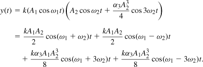
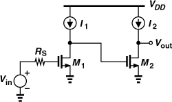
As an example of an RF circuit in which time variance plays a critical role and must not be confused with nonlinearity, let us consider the simple switching circuit shown in Fig. 2.2(a). The control terminal of the switch is driven by vin1(t) = A1 cosω1t and the input terminal by vin2(t) = A2 cos ω2t. We assume the switch is on if vin1 > 0 and off otherwise. Is this system nonlinear or time-variant? If, as depicted in Fig. 2.2(b), the input of interest is vin1 (while vin2 is part of the system and still equal to A2 cos ω2t), then the system is nonlinear because the control is only sensitive to the polarity of vin1 and independent of its amplitude. This system is also time-variant because the output depends on vin2. For example, if vin1 is constant and positive, then vout(t) = vin2(t), and if vin1 is constant and negative, then vout(t) = 0 (why?).
Figure 2.2 (a) Simple switching circuit, (b) system with Vin1 as the input, (c) system with Vin2 as the input.
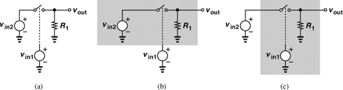
Now consider the case shown in Fig. 2.2(c), where the input of interest is vin2 (while vin1 remains part of the system and still equal to A1 cos ω1t). This system is linear with respect to vin2. For example, doubling the amplitude of vin2 directly doubles that of vout. The system is also time-variant due to the effect of vin1.

The circuit of Fig. 2.2(a) is an example of RF “mixers.” We will study such circuits in Chapter 6 extensively, but it is important to draw several conclusions from the above study. First, statements such as “switches are nonlinear” are ambiguous. Second, a linear system can generate frequency components that do not exist in the input signal—the system only need be time-variant. From Example 2.3,
![]()
where S(t) denotes a square wave toggling between 0 and 1 with a frequency of f1 = ω1/(2π). The output spectrum is therefore given by the convolution of the spectra of vin2(t) and S(t). Since the spectrum of a square wave is equal to a train of impulses whose amplitudes follow a sinc envelope, we have
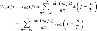
where T1 = 2π/ω1. This operation is illustrated in Fig. 2.4 for a Vin2 spectrum located around zero frequency.1
Figure 2.4 Multiplication in the time domain and corresponding convolution in the frequency domain.

2.1.3 Nonlinearity
A system is called “memoryless” or “static” if its output does not depend on the past values of its input (or the past values of the output itself). For a memoryless linear system, the input/output characteristic is given by
![]()
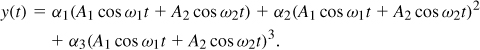
where α is a function of time if the system is time-variant [e.g., Fig. 2.2(c)]. For a memoryless nonlinear system, the input/output characteristic can be approximated with a polynomial,
![]()
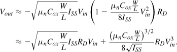
where αj may be functions of time if the system is time-variant. Figure 2.5 shows a common-source stage as an example of a memoryless nonlinear circuit (at low frequencies). If M1 operates in the saturation region and can be approximated as a square-law device, then
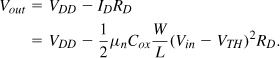
In this idealized case, the circuit displays only second-order nonlinearity.
Figure 2.5 Common-source stage.
The system described by Eq. (2.16) has “odd symmetry” if y(t) is an odd function of x(t), i.e., if the response to − x(t) is the negative of that to + x(t). This occurs if αj = 0 for even j. Such a system is sometimes called “balanced,” as exemplified by the differential pair shown in Fig. 2.6(a). Recall from basic analog design that by virtue of symmetry, the circuit exhibits the characteristic depicted in Fig. 2.6(b) if the differential input varies from very negative values to very positive values.
Figure 2.6 (a) Differential pair and (b) its input/output characteristic.


A system is called “dynamic” if its output depends on the past values of its input(s) or output(s). For a linear, time-invariant, dynamic system,
![]()
where h(t) denotes the impulse response. If a dynamic system is linear but time-variant, its impulse response depends on the time origin; if δ(t) yields h(t), then δ(t − τ) produces h(t, τ). Thus,
![]()
Finally, if a system is both nonlinear and dynamic, then its impulse response can be approximated by a Volterra series. This is described in Section 2.8.
2.2 Effects of Nonlinearity
While analog and RF circuits can be approximated by a linear model for small-signal operation, nonlinearities often lead to interesting and important phenomena that are not predicted by small-signal models. In this section, we study these phenomena for memoryless systems whose input/output characteristic can be approximated by2
![]()
The reader is cautioned, however, that the effect of storage elements (dynamic nonlinearity) and higher-order nonlinear terms must be carefully examined to ensure (2.25) is a plausible representation. Section 2.7 deals with the case of dynamic nonlinearity. We may consider α1 as the small-signal gain of the system because the other two terms are negligible for small input swings. For example, ![]() in Eq. (2.22).
in Eq. (2.22).
The nonlinearity effects described in this section primarily arise from the third-order term in Eq. (2.25). The second-order term too manifests itself in certain types of receivers and is studied in Chapter 4.
2.2.1 Harmonic Distortion
If a sinusoid is applied to a nonlinear system, the output generally exhibits frequency components that are integer multiples (“harmonics”) of the input frequency. In Eq. (2.25), if x(t) = A cos ωt, then
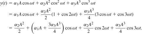
In Eq. (2.28), the first term on the right-hand side is a dc quantity arising from second-order nonlinearity, the second is called the “fundamental,” the third is the second harmonic, and the fourth is the third harmonic. We sometimes say that even-order nonlinearity introduces dc offsets.
From the above expansion, we make two observations. First, even-order harmonics result from αj with even j, and vanish if the system has odd symmetry, i.e., if it is fully differential. In reality, however, random mismatches corrupt the symmetry, yielding finite even-order harmonics. Second, in (2.28) the amplitudes of the second and third harmonics are proportional to A2 and A3, respectively, i.e., we say the nth harmonic grows in proportion to An.
In many RF circuits, harmonic distortion is unimportant or an irrelevant indicator of the effect of nonlinearity. For example, an amplifier operating at 2.4 GHz produces a second harmonic at 4.8 GHz, which is greatly suppressed if the circuit has a narrow bandwidth. Nonetheless, harmonics must always be considered carefully before they are dismissed. The following examples illustrate this point.


2.2.2 Gain Compression
The small-signal gain of circuits is usually obtained with the assumption that harmonics are negligible. However, our formulation of harmonics, as expressed by Eq. (2.28), indicates that the gain experienced by A cos ωt is equal to α1 + 3α3A2/4 and hence varies appreciably as A becomes larger.4 We must then ask, do α1 and α3 have the same sign or opposite signs? Returning to the third-order polynomial in Eq. (2.25), we note that if α1α3 > 0, then α1x + α3x3 overwhelms α2x2 for large x regardless of the sign of α2, yielding an “expansive” characteristic [Fig. 2.9(a)]. For example, an ideal bipolar transistor operating in the forward active region produces a collector current in proportion to exp(VBE/VT), exhibiting expansive behavior. On the other hand, if α1α3 < 0, the term α3x3 “bends” the characteristic for sufficiently large x [Fig. 2.9(b)], leading to “compressive” behavior, i.e., a decreasing gain as the input amplitude increases. For example, the differential pair of Fig. 2.6(a) suffers from compression as the second term in (2.22) becomes comparable with the first. Since most RF circuits of interest are compressive, we hereafter focus on this type.
Figure 2.9 (a) Expansive and (b) compressive characteristics.

With α1α3 < 0, the gain experienced by A cos ωt in Eq. (2.28) falls as A rises. We quantify this effect by the “1-dB compression point,” defined as the input signal level that causes the gain to drop by 1 dB. If plotted on a log-log scale as a function of the input level, the output level, Aout, falls below its ideal value by 1 dB at the 1-dB compression point, Ain,1dB (Fig. 2.10). Note that (a) Ain and Aout are voltage quantities here, but compression can also be expressed in terms of power quantities; (b) 1-dB compression may also be specified in terms of the output level at which it occurs, Aout,1dB. The input and output compression points typically prove relevant in the receive path and the transmit path, respectively.
Figure 2.10 Definition of 1-dB compression point.
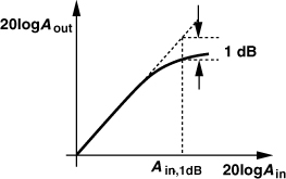
To calculate the input 1-dB compression point, we equate the compressed gain, ![]() , to 1 dB less than the ideal gain, α1:
, to 1 dB less than the ideal gain, α1:
![]()
It follows that

Note that Eq. (2.34) gives the peak value (rather than the peak-to-peak value) of the input. Also denoted by P1dB, the 1-dB compression point is typically in the range of −20 to −25 dBm (63.2 to 35.6 mVpp in 50-Ω system) at the input of RF receivers. We use the notations A1dB and P1dB interchangeably in this book. Whether they refer to the input or the output will be clear from the context or specified explicitly. While gain compression by 1 dB seems arbitrary, the 1-dB compression point represents a 10% reduction in the gain and is widely used to characterize RF circuits and systems.
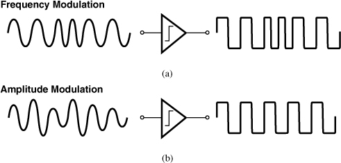
Why does compression matter? After all, it appears that if a signal is so large as to reduce the gain of a receiver, then it must lie well above the receiver noise and be easily detectable. In fact, for some modulation schemes, this statement holds and compression of the receiver would seem benign. For example, as illustrated in Fig. 2.11(a), a frequency-modulated signal carries no information in its amplitude and hence tolerates compression (i.e., amplitude limiting). On the other hand, modulation schemes that contain information in the amplitude are distorted by compression [Fig. 2.11(b)]. This issue manifests itself in both receivers and transmitters.
Figure 2.11 Effect of compressive nonlinearity on (a) FM and (b) AM waveforms.
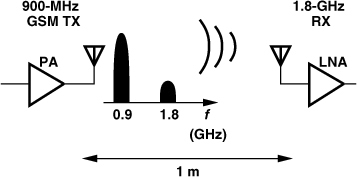
Another adverse effect arising from compression occurs if a large interferer accompanies the received signal [Fig. 2.12(a)]. In the time domain, the small desired signal is superimposed on the large interferer. Consequently, the receiver gain is reduced by the large excursions produced by the interferer even though the desired signal itself is small [Fig. 2.12(b)]. Called “desensitization,” this phenomenon lowers the signal-to-noise ratio (SNR) at the receiver output and proves critical even if the signal contains no amplitude information.
Figure 2.12 (a) Interferer accompanying signal, (b) effect in time domain.

To quantify desensitization, let us assume x(t) = A1 cos ω1t + A2 cos ω2t, where the first and second terms represent the desired component and the interferer, respectively. With the third-order characteristic of Eq. (2.25), the output appears as
![]()
Note that α2 is absent in compression. For A1 ![]() A2, this reduces to
A2, this reduces to
![]()
Thus, the gain experienced by the desired signal is equal to ![]() , a decreasing function of A2 if α1α3 < 0. In fact, for sufficiently large A2, the gain drops to zero, and we say the signal is “blocked.” In RF design, the term “blocking signal” or “blocker” refers to interferers that desensitize a circuit even if they do not reduce the gain to zero. Some RF receivers must be able to withstand blockers that are 60 to 70 dB greater than the desired signal.
, a decreasing function of A2 if α1α3 < 0. In fact, for sufficiently large A2, the gain drops to zero, and we say the signal is “blocked.” In RF design, the term “blocking signal” or “blocker” refers to interferers that desensitize a circuit even if they do not reduce the gain to zero. Some RF receivers must be able to withstand blockers that are 60 to 70 dB greater than the desired signal.
2.2.3 Cross Modulation
Another phenomenon that occurs when a weak signal and a strong interferer pass through a nonlinear system is the transfer of modulation from the interferer to the signal. Called “cross modulation,” this effect is exemplified by Eq. (2.36), where variations in A2 affect the amplitude of the signal at ω1. For example, suppose that the interferer is an amplitude-modulated signal, A2(1 + m cos ωmt) cos ω2t, where m is a constant and ωm denotes the modulating frequency. Equation (2.36) thus assumes the following form:
![]()
In other words, the desired signal at the output suffers from amplitude modulation at ωm and 2ωm. Figure 2.14 illustrates this effect.

Solution:
![]()
We now note that (1) the second-order term yields components at ω1 ± ω2 but not at ω1; (2) the third-order term expansion gives ![]() , which, according to cos2 x = (1 + cos 2x)/2, results in a component at ω1. Thus,
, which, according to cos2 x = (1 + cos 2x)/2, results in a component at ω1. Thus,
![]()
Cross modulation commonly arises in amplifiers that must simultaneously process many independent signal channels. Examples include cable television transmitters and systems employing “orthogonal frequency division multiplexing” (OFDM). We examine OFDM in Chapter 3.
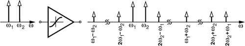
2.2.4 Intermodulation
Our study of nonlinearity has thus far considered the case of a single signal (for harmonic distortion) or a signal accompanied by one large interferer (for desensitization). Another scenario of interest in RF design occurs if two interferers accompany the desired signal. Such a scenario represents realistic situations and reveals nonlinear effects that may not manifest themselves in a harmonic distortion or desensitization test.
If two interferers at ω1 and ω2 are applied to a nonlinear system, the output generally exhibits components that are not harmonics of these frequencies. Called “intermodulation” (IM), this phenomenon arises from “mixing” (multiplication) of the two components as their sum is raised to a power greater than unity. To understand how Eq. (2.25) leads to intermodulation, assume x(t) = A1 cos ω1t + A2 cos ω2t. Thus,
Expanding the right-hand side and discarding the dc terms, harmonics, and components at ω1 ± ω2, we obtain the following “intermodulation products”:
![]()
![]()
and these fundamental components:

Figure 2.15 illustrates the results. Among these, the third-order IM products at 2ω1 − ω2 and 2ω2 − ω1 are of particular interest. This is because, if ω1 and ω2 are close to each other, then 2ω1 − ω2 and 2ω2 − ω1 appear in the vicinity of ω1 and ω2. We now explain the significance of this statement.
Figure 2.15 Generation of various intermodulation components in a two-tone test.
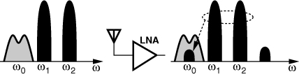
Suppose an antenna receives a small desired signal at ω0 along with two large interferers at ω1 and ω2, providing this combination to a low-noise amplifier (Fig. 2.16). Let us assume that the interferer frequencies happen to satisfy 2ω1 − ω2 = ω0. Consequently, the intermodulation product at 2ω1 − ω2 falls onto the desired channel, corrupting the signal.
Figure 2.16 Corruption due to third-order intermodulation.
The reader may raise several questions at this point: (1) In our analysis of intermodulation, we represented the interferers with pure (unmodulated) sinusoids (called “tones”) whereas in Figs. 2.16 and 2.17, the interferers are modulated. Are these consistent? (2) Can gain compression and desensitization (P1dB) also model intermodulation, or do we need other measures of nonlinearity? (3) Why can we not simply remove the interferers by filters so that the receiver does not experience intermodulation? We answer the first two here and address the third in Chapter 4.
For narrowband signals, it is sometimes helpful to “condense” their energy into an impulse, i.e., represent them with a tone of equal power [Fig. 2.18(a)]. This approximation must be made judiciously: if applied to study gain compression, it yields reasonably accurate results; on the other hand, if applied to the case of cross modulation, it fails. In intermodulation analyses, we proceed as follows: (a) approximate the interferers with tones, (b) calculate the level of intermodulation products at the output, and (c) mentally convert the intermodulation tones back to modulated components so as to see the corruption.5 This thought process is illustrated in Fig. 2.18(b).
Figure 2.18 (a) Approximation of modulated signals by impulses, (b) application to intermodulation.
We now deal with the second question: if the gain is not compressed, then can we say that intermodulation is negligible? The answer is no; the following example illustrates this point.
(a) Determine the value of α3 that yields a P1dB of −30 dBm.
(b) If each interferer is 10 dB below P1dB, determine the corruption experienced by the desired signal at the LNA output.
Solution:
(a) Noting that −30 dBm = 20 mVpp = 10 mVp, from Eq. (2.34), we have ![]() . Since α1 = 10, we obtain α3 = 14, 500 V−2.
. Since α1 = 10, we obtain α3 = 14, 500 V−2.
(b) Each interferer has a level of −40 dBm (= 6.32 mVpp). Setting A1 = A2 = 6.32 mVpp/2 in Eq. (2.41), we determine the amplitude of the IM product at 2.410 GHz as
![]()
The desired signal is amplified by a factor of α1 = 10 = 20 dB, emerging at the output at a level of −60 dBm. Unfortunately, the IM product is as large as the signal itself even though the LNA does not experience significant compression.
The two-tone test is versatile and powerful because it can be applied to systems with arbitrarily narrow bandwidths. A sufficiently small difference between the two tone frequencies ensures that the IM products also fall within the band, thereby providing a meaningful view of the nonlinear behavior of the system. Depicted in Fig. 2.19(a), this attribute stands in contrast to harmonic distortion tests, where higher harmonics lie so far away in frequency that they are heavily filtered, making the system appear quite linear [Fig. 2.19(b)].
Figure 2.19 (a) Two-tone and (b) harmonic tests in a narrowband system.

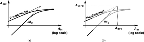
Third Intercept Point
Our thoughts thus far indicate the need for a measure of intermodulation. A common method of IM characterization is the “two-tone” test, whereby two pure sinusoids of equal amplitudes are applied to the input. The amplitude of the output IM products is then normalized to that of the fundamentals at the output. Denoting the peak amplitude of each tone by A, we can write the result as
![]()
where the unit dBc denotes decibels with respect to the “carrier” to emphasize the normalization. Note that, if the amplitude of each input tone increases by 6 dB (a factor of two), the amplitude of the IM products (∝ A3) rises by 18 dB and hence the relative IM by 12 dB.6
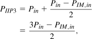
The principal difficulty in specifying the relative IM for a circuit is that it is meaningful only if the value of A is given. From a practical point of view, we prefer a single measure that captures the intermodulation behavior of the circuit with no need to know the input level at which the two-tone test is carried out. Fortunately, such a measure exists and is called the “third intercept point” (IP3).
The concept of IP3 originates from our earlier observation that, if the amplitude of each tone rises, that of the output IM products increases more sharply (∝ A3). Thus, if we continue to raise A, the amplitude of the IM products eventually becomes equal to that of the fundamental tones at the output. As illustrated in Fig. 2.20 on a log-log scale, the input level at which this occurs is called the “input third intercept point” (IIP3). Similarly, the corresponding output is represented by OIP3. In subsequent derivations, we denote the input amplitude as AIIP3.
Figure 2.20 Definition of IP3 (for voltage quantities).
To determine the IIP3, we simply equate the fundamental and IM amplitudes:
![]()
obtaining

Interestingly,
This ratio proves helpful as a sanity check in simulations and measurements.7 We sometimes write IP3 rather than IIP3 if it is clear from the context that the input is of interest.
Upon further consideration, the reader may question the consistency of the above derivations. If the IP3 is 9.6 dB higher than P1dB, is the gain not heavily compressed at Ain = AIIP3?! If the gain is compressed, why do we still express the amplitude of the fundamentals at the output as α1A? It appears that we must instead write this amplitude as [α1 + (9/4)α3A2]A to account for the compression.
In reality, the situation is even more complicated. The value of IP3 given by Eq. (2.47) may exceed the supply voltage, indicating that higher-order nonlinearities manifest themselves as Ain approaches AIIP3 [Fig. 2.21(a)]. In other words, the IP3 is not a directly measureable quantity.
Figure 2.21 (a) Actual behavior of nonlinear circuits, (b) definition of IP3 based on extrapolation.
In order to avoid these quandaries, we measure the IP3 as follows. We begin with a very low input level so that ![]() (and, of course, higher order nonlinearities are also negligible). We increase Ain, plot the amplitudes of the fundamentals and the IM products on a log-log scale, and extrapolate these plots according to their slopes (one and three, respectively) to obtain the IP3 [Fig. 2.21(b)]. To ensure that the signal levels remain well below compression and higher-order terms are negligible, we must observe a 3-dB rise in the IM products for every 1-dB increase in Ain. On the other hand, if Ain is excessively small, then the output IM components become comparable with the noise floor of the circuit (or the noise floor of the simulated spectrum), thus leading to inaccurate results.
(and, of course, higher order nonlinearities are also negligible). We increase Ain, plot the amplitudes of the fundamentals and the IM products on a log-log scale, and extrapolate these plots according to their slopes (one and three, respectively) to obtain the IP3 [Fig. 2.21(b)]. To ensure that the signal levels remain well below compression and higher-order terms are negligible, we must observe a 3-dB rise in the IM products for every 1-dB increase in Ain. On the other hand, if Ain is excessively small, then the output IM components become comparable with the noise floor of the circuit (or the noise floor of the simulated spectrum), thus leading to inaccurate results.
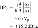
Since extrapolation proves quite tedious in simulations or measurements, we often employ a shortcut that provides a reasonable initial estimate. As illustrated in Fig. 2.22(a), suppose hypothetically that the input is equal to AIIP3, and hence the (extrapolated) output IM products are as large as the (extrapolated) fundamental tones. Now, the input is reduced to a level Ain1. That is, the change in the input is equal to 20 log AIIP3 − 20 log Ain1. On a log-log scale, the IM products fall with a slope of 3 and the fundamentals with a slope of unity. Thus, the difference between the two plots increases with a slope of 2. We denote 20 log Af − 20 log AIM by Δ P and write
![]()
obtaining
![]()
Figure 2.22 (a) Relationships among various power levels in a two-tone test, (b) illustration of shortcut technique.

In other words, for a given input level (well below P1dB), the IIP3 can be calculated by halving the difference between the output fundamental and IM levels and adding the result to the input level, where all values are expressed as logarithmic quantities. Figure 2.22(b) depicts an abbreviated notation for this rule. The key point here is that the IP3 is measured without extrapolation.
Why do we consider the above result an estimate? After all, the derivation assumes third-order nonlinearity. A difficulty arises if the circuit contains dynamic nonlinearities, in which case this result may deviate from that obtained by extrapolation. The latter is the standard and accepted method for measuring and reporting the IP3, but the shortcut method proves useful in understanding the behavior of the device under test.
We should remark that second-order nonlinearity also leads to a certain type of intermodulation and is characterized by a “second intercept point,” (IP2).8 We elaborate on this effect in Chapter 4.
2.2.5 Cascaded Nonlinear Stages
Since in RF systems, signals are processed by cascaded stages, it is important to know how the nonlinearity of each stage is referred to the input of the cascade. The calculation of P1dB for a cascade is outlined in Problem 2.1. Here, we determine the IP3 of a cascade. For the sake of brevity, we hereafter denote the input IP3 by AIP3 unless otherwise noted.
Consider two nonlinear stages in cascade (Fig. 2.23). If the input/output characteristics of the two stages are expressed, respectively, as
![]()
![]()
then
![]()
Figure 2.23 Cascaded nonlinear stages.
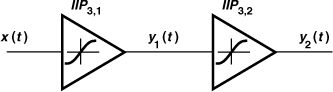
Considering only the first- and third-order terms, we have
![]()
Thus, from Eq. (2.47),

Solution:
With no asymmetries in the cascade, α2 = β2 = 0. Thus, we seek the condition ![]() , or equivalently,
, or equivalently,
![]()
Equation (2.61) leads to more intuitive results if its two sides are squared and inverted:
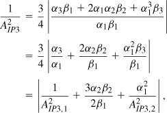
where AIP3,1 and AIP3,2 represent the input IP3’s of the first and second stages, respectively. Note that AIP3, AIP3,1, and AIP3,2 are voltage quantities.
The key observation in Eq. (2.65) is that to “refer” the IP3 of the second stage to the input of the cascade, we must divide it by α1. Thus, the higher the gain of the first stage, the more nonlinearity is contributed by the second stage.
IM Spectra in a Cascade
To gain more insight into the above results, let us assume x(t) = A cos ω1t + A cos ω2t and identify the IM products in a cascade. With the aid of Fig. 2.24, we make the following observations:9
1. The input tones are amplified by a factor of approximately α1 in the first stage and β1 in the second. Thus, the output fundamentals are given by α1β1A(cos ω1t + cos ω2t).
2. The IM products generated by the first stage, namely, (3α3/4)A3[cos(2ω1 − ω2)t + cos(2ω2 − ω1)t], are amplified by a factor of β1 when they appear at the output of the second stage.
3. Sensing α1A(cos ω1t + cos ω2t) at its input, the second stage produces its own IM components: (3β3/4)(α1A)3cos(2ω1 − ω2)t + (3β3/4)(α1A)3cos(2ω2 − ω1)t.
4. The second-order nonlinearity in y1(t) generates components at ω1 − ω2, 2ω1, and 2ω2. Upon experiencing a similar nonlinearity in the second stage, these components are mixed with those at ω1 and ω2 and translated to 2ω1 − ω2 and 2ω2 − ω1. Specifically, as shown in Fig. 2.24, y2(t) contains terms such as 2β2[α1A cos ω1t × α2A2cos(ω1 − ω2)t] and 2β2(α1A cos ω1t × 0.5α2A2cos 2ω2t). The resulting IM products can be expressed as (3α1α2β2A3/2)[cos(2ω1 − ω2)t + cos(2ω2 − ω1)t]. Interestingly, the cascade of two second-order nonlinearities can produce third-order IM products.
Figure 2.24 Spectra in a cascade of nonlinear stages.

Adding the amplitudes of the IM products, we have
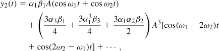
obtaining the same IP3 as above. This result assumes zero phase shift for all components.
Why did we add the amplitudes of the IM3 products in Eq. (2.66) without regard for their phases? Is it possible that phase shifts in the first and second stages allow partial cancellation of these terms and hence a higher IP3? Yes, it is possible but uncommon in practice. Since the frequencies ω1, ω2, 2ω1 − ω2, and 2ω2 − ω1 are close to one another, these components experience approximately equal phase shifts.
But how about the terms described in the fourth observation? Components such as ω1 − ω2 and 2ω1 may fall well out of the signal band and experience phase shifts different from those in the first three observations. For this reason, we may consider Eqs. (2.65) and (2.66) as the worst-case scenario. Since most RF systems incorporate narrowband circuits, the terms at ω1 ± ω2, 2ω1, and 2ω2 are heavily attenuated at the output of the first stage. Consequently, the second term on the right-hand side of (2.65) becomes negligible, and
![]()
Extending this result to three or more stages, we have
![]()
Thus, if each stage in a cascade has a gain greater than unity, the nonlinearity of the latter stages becomes increasingly more critical because the IP3 of each stage is equivalently scaled down by the total gain preceding that stage.
In the simulation of a cascade, it is possible to determine which stage limits the linearity more. As depicted in Fig. 2.25, we examine the relative IM magnitudes at the output of each stage (Δ1 and Δ2, expressed in dB.) If Δ2 ≈ Δ1, the second stage contributes negligible nonlinearity. On the other hand, if Δ2 is substantially less than Δ1, then the second stage limits the IP3.
Figure 2.25 Growth of IM components along the cascade.
2.2.6 AM/PM Conversion
In some RF circuits, e.g., power amplifiers, amplitude modulation (AM) may be converted to phase modulation (PM), thus producing undesirable effects. In this section, we study this phenomenon.
AM/PM conversion (APC) can be viewed as the dependence of the phase shift upon the signal amplitude. That is, for an input Vin(t) = V1 cos ω1t, the fundamental output component is given by
![]()
where φ(V1) denotes the amplitude-dependent phase shift. This, of course, does not occur in a linear time-invariant system. For example, the phase shift experienced by a sinusoid of frequency ω1 through a first-order low-pass RC section is given by − tan−1(RCω1) regardless of the amplitude. Moreover, APC does not appear in a memoryless nonlinear system because the phase shift is zero in this case.
We may therefore surmise that AM/PM conversion arises if a system is both dynamic and nonlinear. For example, if the capacitor in a first-order low-pass RC section is nonlinear, then its “average” value may depend on V1, resulting in a phase shift, − tan−1 (RCω1), that itself varies with V1. To explore this point, let us consider the arrangement shown in Fig. 2.26 and assume
![]()
![]()
Figure 2.26 RC section with nonlinear capacitor.
This capacitor is considered nonlinear because its value depends on its voltage. An exact calculation of the phase shift is difficult here as it requires that we write Vin = R1C1dVout/dt + Vout and hence solve
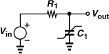
We therefore make an approximation. Since the value of C1 varies periodically with time, we can express the output as that of a first-order network but with a time-varying capacitance, C1(t):
If R1C1(t)ω1 ![]() 1 rad,
1 rad,
![]()
We also assume that (1 + αVout)C0 ≈ (1 + αV1 cos ω1t)C0, obtaining
![]()
Does the output fundamental contain an input-dependent phase shift here? No, it does not! The reader can show that the third term inside the parentheses produces only higher harmonics. Thus, the phase shift of the fundamental is equal to −R1C0ω1 and hence constant.
The above example entails no AM/PM conversion because of the first-order dependence of C1 upon Vout. As illustrated in Fig. 2.27, the average value of C1 is equal to C0 regardless of the output amplitude. In general, since C1 varies periodically, it can be expressed as a Fourier series with a “dc” term representing its average value:
![]()
Figure 2.27 Time variation of capacitor with first-order voltage dependence for small and large swings.

Thus, if Cavg is a function of the amplitude, then the phase shift of the fundamental component in the output voltage becomes input-dependent. The following example illustrates this point.
Suppose C1 in Fig. 2.26 is expressed as ![]() . Study the AM/PM conversion in this case if Vin(t) = V1 cos ω1t.
. Study the AM/PM conversion in this case if Vin(t) = V1 cos ω1t.
Solution:
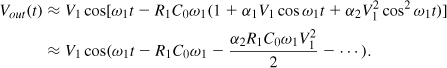
Figure 2.28 Time variation of capacitor with second-order voltage dependence for small and large swings.
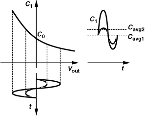
The phase shift of the fundamental now contains an input-dependent term, ![]() . Figure 2.28 also suggests that AM/PM conversion does not occur if the capacitor voltage dependence is odd-symmetric.
. Figure 2.28 also suggests that AM/PM conversion does not occur if the capacitor voltage dependence is odd-symmetric.
What is the effect of APC? In the presence of APC, amplitude modulation (or amplitude noise) corrupts the phase of the signal. For example, if Vin(t) = V1(1 + m cos ωmt) cos ω1t, then Eq. (2.79) yields a phase corruption equal to ![]() . We will encounter examples of APC in Chapters 8 and 12.
. We will encounter examples of APC in Chapters 8 and 12.
2.3 Noise
The performance of RF systems is limited by noise. Without noise, an RF receiver would be able to detect arbitrarily small inputs, allowing communication across arbitrarily long distances. In this section, we review basic properties of noise and methods of calculating noise in circuits. For a more complete study of noise in analog circuits, the reader is referred to [1].
2.3.1 Noise as a Random Process
The trouble with noise is that it is random. Engineers who are used to dealing with well-defined, deterministic, “hard” facts often find the concept of randomness difficult to grasp, especially if it must be incorporated mathematically. To overcome this fear of randomness, we approach the problem from an intuitive angle.
By “noise is random,” we mean the instantaneous value of noise cannot be predicted. For example, consider a resistor tied to a battery and carrying a current [Fig. 2.29(a)]. Due to the ambient temperature, each electron carrying the current experiences thermal agitation, thus following a somewhat random path while, on the average, moving toward the positive terminal of the battery. As a result, the average current remains equal to VB/R but the instantaneous current displays random values.10
Figure 2.29 (a) Noise generated in a resistor, (b) effect of higher temperature.

Since noise cannot be characterized in terms of instantaneous voltages or currents, we seek other attributes of noise that are predictable. For example, we know that a higher ambient temperature leads to greater thermal agitation of electrons and hence larger fluctuations in the current [Fig. 2.29(b)]. How do we express the concept of larger random swings for a current or voltage quantity? This property is revealed by the average power of the noise, defined, in analogy with periodic signals, as
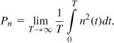
where n(t) represents the noise waveform. Illustrated in Fig. 2.30, this definition simply means that we compute the area under n2(t) for a long time, T, and normalize the result to T, thus obtaining the average power. For example, the two scenarios depicted in Fig. 2.29 yield different average powers.
Figure 2.30 Computation of noise power.
If n(t) is random, how do we know that Pn is not?! We are fortunate that noise components in circuits have a constant average power. For example, Pn is known and constant for a resistor at a constant ambient temperature.
How long should T in Eq. (2.80) be? Due to its randomness, noise consists of different frequencies. Thus, T must be long enough to accommodate several cycles of the lowest frequency. For example, the noise in a crowded restaurant arises from human voice and covers the range of 20 Hz to 20 kHz, requiring that T be on the order of 0.5 s to capture about 10 cycles of the 20-Hz components.11
2.3.2 Noise Spectrum
Our foregoing study suggests that the time-domain view of noise provides limited information, e.g., the average power. The frequency-domain view, on the other hand, yields much greater insight and proves more useful in RF design.
The reader may already have some intuitive understanding of the concept of “spectrum.” We say the spectrum of human voice spans the range of 20 Hz to 20 kHz. This means that if we somehow measure the frequency content of the voice, we observe all components from 20 Hz to 20 kHz. How, then, do we measure a signal’s frequency content, e.g., the strength of a component at 10 kHz? We would need to filter out the remainder of the spectrum and measure the average power of the 10-kHz component. Figure 2.31(a) conceptually illustrates such an experiment, where the microphone signal is applied to a band-pass filter having a 1-Hz bandwidth centered around 10 kHz. If a person speaks into the microphone at a steady volume, the power meter reads a constant value.
Figure 2.31 Measurement of (a) power in 1 Hz, and (b) the spectrum.

The scheme shown in Fig. 2.31(a) can be readily extended so as to measure the strength of all frequency components. As depicted in Fig. 2.31(b), a bank of 1-Hz band-pass filters centered at f1 ... fn measures the average power at each frequency.12 Called the spectrum or the “power spectral density” (PSD) of x(t) and denoted by Sx(f), the resulting plot displays the average power that the voice (or the noise) carries in a 1-Hz bandwidth at different frequencies.13
It is interesting to note that the total area under Sx(f) represents the average power carried by x(t):
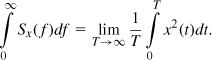
The spectrum shown in Fig. 2.31(b) is called “one-sided” because it is constructed for positive frequencies. In some cases, the analysis is simpler if a “two-sided” spectrum is utilized. The latter is an even-symmetric of the former scaled down vertically by a factor of two (Fig. 2.32), so that the two carry equal energies.
Figure 2.32 Two-sided and one-sided spectra.
![]()
(a) What is the total average power carried by the noise voltage?
(b) What is the dimension of Sv(f)?
(c) Calculate the noise voltage for a 50-Ω resistor in 1 Hz at room temperature.
Solution:
(a) The area under Sv(f) appears to be infinite, an implausible result because the resistor noise arises from the finite ambient heat. In reality, Sv(f) begins to fall at f > 1 THz, exhibiting a finite total energy, i.e., thermal noise is not quite white.
(b) The dimension of Sv(f) is voltage squared per unit bandwidth (V2/Hz) rather than power per unit bandwidth (W/Hz). In fact, we may write the PSD as
![]()
where ![]() denotes the average power of Vn in 1 Hz.14 While some texts express the right-hand side as 4kTRΔf to indicate the total noise in a bandwidth of Δf, we omit Δf with the understanding that our PSDs always represent power in 1 Hz. We shall use Sv(f) and
denotes the average power of Vn in 1 Hz.14 While some texts express the right-hand side as 4kTRΔf to indicate the total noise in a bandwidth of Δf, we omit Δf with the understanding that our PSDs always represent power in 1 Hz. We shall use Sv(f) and ![]() interchangeably.
interchangeably.
(c) For a 50-Ω resistor at T = 300 K,
![]()
This means that if the noise voltage of the resistor is applied to a 1-Hz band-pass filter centered at any frequency (< 1 THz), then the average measured output is given by the above value. To express the result as a root-mean-squared (rms) quantity and in more familiar units, we may take the square root of both sides:
![]()
The familiar unit is nV but the strange unit is ![]() . The latter bears no profound meaning; it simply says that the average power in 1 Hz is (0.91 nV)2.
. The latter bears no profound meaning; it simply says that the average power in 1 Hz is (0.91 nV)2.
2.3.3 Effect of Transfer Function on Noise
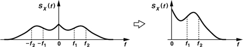
The principal reason for defining the PSD is that it allows many of the frequency-domain operations used with deterministic signals to be applied to random signals as well. For example, if white noise is applied to a low-pass filter, how do we determine the PSD at the output? As shown in Fig. 2.33, we intuitively expect that the output PSD assumes the shape of the filter’s frequency response. In fact, if x(t) is applied to a linear, time-invariant system with a transfer function H(s), then the output spectrum is
![]()
where H(f) = H(s = j2πf) [2]. We note that |H(f)| is squared because Sx(f) is a (voltage or current) squared quantity.
Figure 2.33 Effect of low-pass filter on white noise.
2.3.4 Device Noise
In order to analyze the noise performance of circuits, we wish to model the noise of their constituent elements by familiar components such as voltage and current sources. Such a representation allows the use of standard circuit analysis techniques.
Thermal Noise of Resistors
As mentioned previously, the ambient thermal energy leads to random agitation of charge carriers in resistors and hence noise. The noise can be modeled by a series voltage source with a PSD of ![]() [Thevenin equivalent, Fig. 2.34(a)] or a parallel current source with a PSD of
[Thevenin equivalent, Fig. 2.34(a)] or a parallel current source with a PSD of ![]() [Norton equivalent, Fig. 2.34(b)]. The choice of the model sometimes simplifies the analysis. The polarity of the sources is unimportant (but must be kept the same throughout the calculations of a given circuit).
[Norton equivalent, Fig. 2.34(b)]. The choice of the model sometimes simplifies the analysis. The polarity of the sources is unimportant (but must be kept the same throughout the calculations of a given circuit).
Figure 2.34 (a) Thevenin and (b) Norton models of resistor thermal noise.
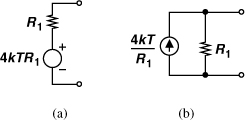
Figure 2.35 (a) RLC tank, (b) inclusion of resistor noise, (c) output noise spectrum due to R1.
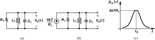
Solution:
Modeling the noise of R1 by a current source, ![]() , [Fig. 2.35(b)] and noting that the transfer function Vn/In1 is, in fact, equal to the impedance of the tank, ZT, we write from Eq. (2.86)
, [Fig. 2.35(b)] and noting that the transfer function Vn/In1 is, in fact, equal to the impedance of the tank, ZT, we write from Eq. (2.86)
![]()
At ![]() , L1 and C1 resonate, reducing the circuit to only R1. Thus, the output noise at f0 is simply equal to
, L1 and C1 resonate, reducing the circuit to only R1. Thus, the output noise at f0 is simply equal to ![]() . At lower or higher frequencies, the impedance of the tank falls and so does the output noise [Fig. 2.35(c)].
. At lower or higher frequencies, the impedance of the tank falls and so does the output noise [Fig. 2.35(c)].
If a resistor converts the ambient heat to a noise voltage or current, can we extract energy from the resistor? In particular, does the arrangement shown in Fig. 2.36 deliver energy to R2? Interestingly, if R1 and R2 reside at the same temperature, no net energy is transferred between them because R2 also produces a noise PSD of 4kTR2 (Problem 2.8). However, suppose R2 is held at T = 0 K. Then, R1 continues to draw thermal energy from its environment, converting it to noise and delivering the energy to R2. The average power transferred to R2 is equal to
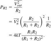
Figure 2.36 Transfer of noise from one resistor to another.
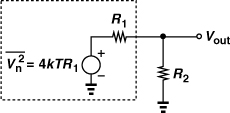
This quantity reaches a maximum if R2 = R1:
![]()
Called the “available noise power,” kT is independent of the resistor value and has the dimension of power per unit bandwidth. The reader can prove that kT = −173.8 dBm/Hz at T = 300 K.
For a circuit to exhibit a thermal noise density of ![]() , it need not contain an explicit resistor of value R1. After all, Eq. (2.86) suggests that the noise density of a resistor may be transformed to a higher or lower value by the surrounding circuit. We also note that if a passive circuit dissipates energy, then it must contain a physical resistance15 and must therefore produce thermal noise. We loosely say “lossy circuits are noisy.”
, it need not contain an explicit resistor of value R1. After all, Eq. (2.86) suggests that the noise density of a resistor may be transformed to a higher or lower value by the surrounding circuit. We also note that if a passive circuit dissipates energy, then it must contain a physical resistance15 and must therefore produce thermal noise. We loosely say “lossy circuits are noisy.”
A theorem that consolidates the above observations is as follows: If the real part of the impedance seen between two terminals of a passive (reciprocal) network is equal to Re{Zout}, then the PSD of the thermal noise seen between these terminals is given by ![]() (Fig. 2.37) [8]. This general theorem is not limited to lumped circuits. For example, consider a transmitting antenna that dissipates energy by radiation according to the equation
(Fig. 2.37) [8]. This general theorem is not limited to lumped circuits. For example, consider a transmitting antenna that dissipates energy by radiation according to the equation ![]() , where Rrad is the “radiation resistance” [Fig. 2.38(a)]. As a receiving element [Fig. 2.38(b)], the antenna generates a thermal noise PSD of16
, where Rrad is the “radiation resistance” [Fig. 2.38(a)]. As a receiving element [Fig. 2.38(b)], the antenna generates a thermal noise PSD of16
![]()
Figure 2.37 Output noise of a passive (reciprocal) circuit.
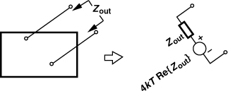
Figure 2.38 (a) Transmitting antenna, (b) receiving antenna producing thermal noise.

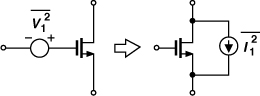
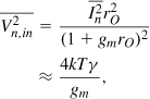
Noise in MOSFETs
The thermal noise of MOS transistors operating in the saturation region is approximated by a current source tied between the source and drain terminals [Fig. 2.39(a)]:
![]()
where γ is the “excess noise coefficient” and gm the transconductance.17 The value of γ is 2/3 for long-channel transistors and may rise to even 2 in short-channel devices [4]. The actual value of γ has other dependencies [5] and is usually obtained by measurements for each generation of CMOS technology. In Problem 2.10, we prove that the noise can alternatively be modeled by a voltage source ![]() in series with the gate [Fig. 2.39(b)].
in series with the gate [Fig. 2.39(b)].
Figure 2.39 Thermal channel noise of a MOSFET modeled as a (a) current source, (b) voltage source.

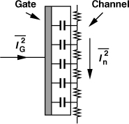
Another component of thermal noise arises from the gate resistance of MOSFETs, an effect that becomes increasingly more important as the gate length is scaled down. Illustrated in Fig. 2.40(a) for a device with a width of W and a length of L, this resistance amounts to
![]()
where ![]() denotes the sheet resistance (resistance of one square) of the polysilicon gate. For example, if W = 1 μm, L = 45 nm, and
denotes the sheet resistance (resistance of one square) of the polysilicon gate. For example, if W = 1 μm, L = 45 nm, and ![]() = 15 Ω, then RG = 333 Ω. Since RG is distributed over the width of the transistor [Fig. 2.40(b)], its noise must be calculated carefully. As proved in [6], the structure can be reduced to a lumped model having an equivalent gate resistance of RG/3 with a thermal noise PSD of 4kTRG/3 [Fig. 2.40(c)]. In a good design, this noise must be much less than that of the channel:
= 15 Ω, then RG = 333 Ω. Since RG is distributed over the width of the transistor [Fig. 2.40(b)], its noise must be calculated carefully. As proved in [6], the structure can be reduced to a lumped model having an equivalent gate resistance of RG/3 with a thermal noise PSD of 4kTRG/3 [Fig. 2.40(c)]. In a good design, this noise must be much less than that of the channel:
![]()
Figure 2.40 (a) Gate resistance of a MOSFET, (b) equivalent circuit for noise calculation, (c) equivalent noise and resistance in lumped model.

The gate and drain terminals also exhibit physical resistances, which are minimized through the use of multiple fingers.
At very high frequencies the thermal noise current flowing through the channel couples to the gate capacitively, thus generating a “gate-induced noise current” [3] (Fig. 2.41). This effect is not modeled in typical circuit simulators, but its significance has remained unclear. In this book, we neglect the gate-induced noise current.
Figure 2.41 Gate-induced noise, ![]() .
.
MOS devices also suffer from “flicker” or “1/f” noise. Modeled by a voltage source in series with the gate, this noise exhibits the following PSD:
![]()
where K is a process-dependent constant. In most CMOS technologies, K is lower for PMOS devices than for NMOS transistors because the former carry charge well below the silicon-oxide interface and hence suffer less from “surface states” (dangling bonds) [1]. The 1/f dependence means that noise components that vary slowly assume a large amplitude. The choice of the lowest frequency in the noise integration depends on the time scale of interest and/or the spectrum of the desired signal [1].
For a given device size and bias current, the 1/f noise PSD intercepts the thermal noise PSD at some frequency, called the “1/f noise corner frequency,” fc. Illustrated in Fig. 2.43, fc can be obtained by converting the flicker noise voltage to current (according to the above example) and equating the result to the thermal noise current:
![]()
It follows that
![]()
Figure 2.43 Flicker noise corner frequency.
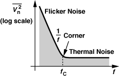
The corner frequency falls in the range of tens or even hundreds of megahertz in today’s MOS technologies.
While the effect of flicker noise may seem negligible at high frequencies, we must note that nonlinearity or time variance in circuits such as mixers and oscillators may translate the 1/f-shaped spectrum to the RF range. We study these phenomena in Chapters 6 and 8.
Noise in Bipolar Transistors
Bipolar transistors contain physical resistances in their base, emitter, and collector regions, all of which generate thermal noise. Moreover, they also suffer from “shot noise” associated with the transport of carriers across the base-emitter junction. As shown in Fig. 2.44, this noise is modeled by two current sources having the following PSDs:
![]()
![]()
where IB and IC are the base and collector bias currents, respectively. Since gm =IC/(kT/q) for bipolar transistors, the collector current shot noise is often expressed as
![]()
in analogy with the thermal noise of MOSFETs or resistors.
Figure 2.44 Noise sources in a bipolar transistor.
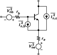
In low-noise circuits, the base resistance thermal noise and the collector current shot noise become dominant. For this reason, wide transistors biased at high current levels are employed.
2.3.5 Representation of Noise in Circuits
With the noise of devices formulated above, we now wish to develop measures of the noise performance of circuits, i.e., metrics that reveal how noisy a given circuit is.
Input-Referred Noise
How can the noise of a circuit be observed in the laboratory? We have access only to the output and hence can measure only the output noise. Unfortunately, the output noise does not permit a fair comparison between circuits: a circuit may exhibit high output noise because it has a high gain rather than high noise. For this reason, we “refer” the noise to the input.
In analog design, the input-referred noise is modeled by a series voltage source and a parallel current source (Fig. 2.45) [1]. The former is obtained by shorting the input port of models A and B and equating their output noises (or, equivalently, dividing the output noise by the voltage gain). Similarly, the latter is computed by leaving the input ports open and equating the output noises (or, equivalently, dividing the output noise by the transimpedance gain).
Figure 2.45 Input-referred noise.
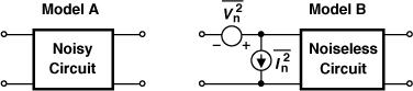
Figure 2.46 (a) CG stage, (b) computation of input-referred noise voltage, (c) computation of input-referred noise current.
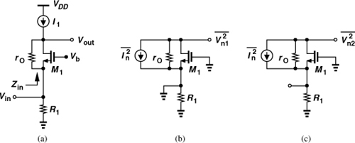
Solution:
![]()
where it is assumed gmrO![]() 1. Leaving the input open as shown in Fig. 2.46(c), the reader can show that (Problem 2.12)
1. Leaving the input open as shown in Fig. 2.46(c), the reader can show that (Problem 2.12)
![]()

From the above example, it may appear that the noise of M1 is “counted” twice. It can be shown that [1] the two input-referred noise sources are necessary and sufficient, but often correlated.
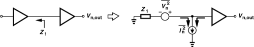
Solution:
Modeling the noise of the circuit by input-referred sources as shown in Fig. 2.47, we observe that some of ![]() flows through Z1, generating a noise voltage at the input that depends on |Z1|. Thus, the output noise, Vn,out, also depends on |Z1|.
flows through Z1, generating a noise voltage at the input that depends on |Z1|. Thus, the output noise, Vn,out, also depends on |Z1|.
Figure 2.47 Noise in a cascade.
The computation and use of input-referred noise sources prove difficult at high frequencies. For example, it is quite challenging to measure the transimpedance gain of an RF stage. For this reason, RF designers employ the concept of “noise figure” as another metric of noise performance that more easily lends itself to measurement.
Noise Figure
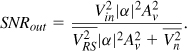
In circuit and system design, we are interested in the signal-to-noise ratio (SNR), defined as the signal power divided by the noise power. It is therefore helpful to ask, how does the SNR degrade as the signal travels through a given circuit? If the circuit contains no noise, then the output SNR is equal to the input SNR even if the circuit acts as an attenuator.18 To quantify how noisy the circuit is, we define its noise figure (NF) as
![]()
such that it is equal to 1 for a noiseless stage. Since each quantity in this ratio has a dimension of power (or voltage squared), we express NF in decibels as
![]()
Note that most texts call (2.109) the “noise factor” and (2.110) the noise figure. We do not make this distinction in this book.
Compared to input-referred noise, the definition of NF in (2.109) may appear rather complicated: it depends on not only the noise of the circuit under consideration but the SNR provided by the preceding stage. In fact, if the input signal contains no noise, then SNRin = ∞ and NF = ∞, even though the circuit may have finite internal noise. For such a case, NF is not a meaningful parameter and only the input-referred noise can be specified.
Calculation of the noise figure is generally simpler than Eq. (2.109) may suggest. For example, suppose a low-noise amplifier senses the signal received by an antenna [Fig. 2.48(a)]. As predicted by Eq. (2.92), the antenna “radiation resistance,” RS, produces thermal noise, leading to the model shown in Fig. 2.48(b). Here, ![]() represents the thermal noise of the antenna, and
represents the thermal noise of the antenna, and ![]() the output noise of the LNA. We must compute SNRin at the LNA input and SNRout at its output.
the output noise of the LNA. We must compute SNRin at the LNA input and SNRout at its output.
Figure 2.48 (a) Antenna followed by LNA, (b) equivalent circuit.
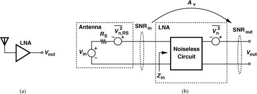
If the LNA exhibits an input impedance of Zin, then both Vin and VRS experience an attenuation factor of α = Zin/(Zin + RS) as they appear at the input of the LNA. That is,

where Vin denotes the rms value of the signal received by the antenna.
To determine SNRout, we assume a voltage gain of Av from the LNA input to the output and recognize that the output signal power is equal to ![]() . The output noise consists of two components: (a) the noise of the antenna amplified by the LNA,
. The output noise consists of two components: (a) the noise of the antenna amplified by the LNA, ![]() , and (b) the output noise of the LNA,
, and (b) the output noise of the LNA, ![]() . Since these two components are uncorrelated, we simply add the PSDs and write
. Since these two components are uncorrelated, we simply add the PSDs and write
It follows that

This result leads to another definition of the NF: the total noise at the output divided by the noise at the output due to the source impedance. The NF is usually specified for a 1-Hz bandwidth at a given frequency, and hence sometimes called the “spot noise figure” to emphasize the small bandwidth.
Equation (2.115) suggests that the NF depends on the source impedance, not only through ![]() but also through
but also through ![]() (Example 2.19). In fact, if we model the noise by input-referred sources, then the input noise current,
(Example 2.19). In fact, if we model the noise by input-referred sources, then the input noise current, ![]() , partially flows through RS, generating a source-dependent noise voltage of
, partially flows through RS, generating a source-dependent noise voltage of ![]() at the input and hence a proportional noise at the output. Thus, the NF must be specified with respect to a source impedance—typically 50 Ω.
at the input and hence a proportional noise at the output. Thus, the NF must be specified with respect to a source impedance—typically 50 Ω.
For hand analysis and simulations, it is possible to reduce the right-hand side of Eq. (2.114) to a simpler form by noting that the numerator is the total noise measured at the output:
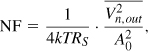
where ![]() includes both the source impedance noise and the LNA noise, and A0 = |α|Av is the voltage gain from Vin to Vout (rather than the gain from the LNA input to its output). We loosely say, “to calculate the NF, we simply divide the total output noise by the gain from Vin to Vout and normalize the result to the noise of RS.” Alternatively, we can say from (2.115) that “we calculate the output noise due to the amplifier (
includes both the source impedance noise and the LNA noise, and A0 = |α|Av is the voltage gain from Vin to Vout (rather than the gain from the LNA input to its output). We loosely say, “to calculate the NF, we simply divide the total output noise by the gain from Vin to Vout and normalize the result to the noise of RS.” Alternatively, we can say from (2.115) that “we calculate the output noise due to the amplifier (![]() ), divide it by the gain, normalize it to 4kTRS, and add 1 to the result.”
), divide it by the gain, normalize it to 4kTRS, and add 1 to the result.”
It is important to note that the above derivations are valid even if no actual power is transferred from the antenna to the LNA or from the LNA to a load. For example, if Zin in Fig. 2.48(b) goes to infinity, no power is delivered to the LNA, but all of the derivations remain valid because they are based on voltage (squared) quantities rather than power quantities. In other words, so long as the derivations incorporate noise and signal voltages, no inconsistency arises in the presence of impedance mismatches or even infinite input impedances. This is a critical difference in thinking between modern RF design and traditional microwave design.
Figure 2.49 (a) Circuit consisting of a single parallel resistor, (b) model for NF calculation.

Solution:
![]()
![]()

Figure 2.50 (a) CS stage, (b) inclusion of noise.
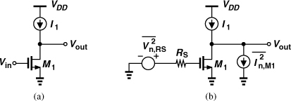
Solution:
From Fig. 2.50(b), the output noise consists of two components: (a) that due to M1, ![]() , and (b) the amplified noise of RS,
, and (b) the amplified noise of RS, ![]() . It follows that
. It follows that
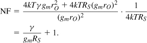
Noise Figure of Cascaded Stages
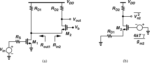
Since many stages appear in a receiver chain, it is desirable to determine the NF of the overall cascade in terms of that of each stage. Consider the cascade depicted in Fig. 2.51(a), where Av1 and Av2 denote the unloaded voltage gain of the two stages. The input and output impedances and the output noise voltages of the two stages are also shown.19
Figure 2.51 (a) Noise in a cascade of stages, (b) simplified diagram.
We first obtain the NF of the cascade using a direct method; according to (2.115), we simply calculate the total noise at the output due to the two stages, divide by (Vout/Vin)2, normalize to 4kTRS, and add one to the result. Taking the loadings into account, we write the overall voltage gain as
![]()
The output noise due to the two stages, denoted by ![]() , consists of two components: (a)
, consists of two components: (a) ![]() , and (b)
, and (b) ![]() amplified by the second stage. Since Vn1 sees an impedance of Rout1 to its left and Rin2 to its right, it is scaled by a factor of Rin2/(Rin2 + Rout1) as it appears at the input of the second stage. Thus,
amplified by the second stage. Since Vn1 sees an impedance of Rout1 to its left and Rin2 to its right, it is scaled by a factor of Rin2/(Rin2 + Rout1) as it appears at the input of the second stage. Thus,
![]()
The overall NF is therefore expressed as
The first two terms constitute the NF of the first stage, NF1, with respect to a source impedance of RS. The third term represents the noise of the second stage, but how can it be expressed in terms of the noise figure of this stage?
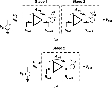
Let us now consider the second stage by itself and determine its noise figure with respect to a source impedance of Rout1 [Fig. 2.51(b)]. Using (2.115) again, we have
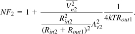
It follows from (2.126) and (2.127) that
What does the denominator represent? This quantity is in fact the “available power gain” of the first stage, defined as the “available power” at its output, Pout,av (the power that it would deliver to a matched load) divided by the available source power, PS,av (the power that the source would deliver to a matched load). This can be readily verified by finding the power that the first stage in Fig. 2.51(a) would deliver to a load equal to Rout1:
![]()
Similarly, the power that Vin would deliver to a load of RS is given by
![]()
The ratio of (2.129) and (2.130) is indeed equal to the denominator in (2.128).
With these observations, we write
![]()
where AP1 denotes the “available power gain” of the first stage. It is important to bear in mind that NF2 is computed with respect to the output impedance of the first stage. For m stages,
![]()
Called “Friis’ equation” [7], this result suggests that the noise contributed by each stage decreases as the total gain preceding that stage increases, implying that the first few stages in a cascade are the most critical. Conversely, if a stage suffers from attenuation (loss), then the NF of the following circuits is “amplified” when referred to the input of that stage.
Figure 2.52 Cascade of CS stages for noise figure calculation.
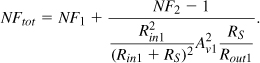
Solution:
![]()
where ![]() ,
, ![]() , Av1 = gm1rO1, and Av2 = gm2rO2. With all of these quantities readily available, we simply substitute for their values in (2.133), obtaining
, Av1 = gm1rO1, and Av2 = gm2rO2. With all of these quantities readily available, we simply substitute for their values in (2.133), obtaining
![]()
The foregoing example represents a typical situation in modern RF design: the interface between the two stages does not have a 50-Ω impedance and no attempt has been made to provide impedance matching between the two stages. In such cases, Friis’ equation becomes cumbersome, making direct calculation of the NF more attractive.
While the above example assumes an infinite input impedance for the second stage, the direct method can be extended to more realistic cases with the aid of Eq. (2.126). Even in the presence of complex input and output impedances, Eq. (2.126) indicates that (1) ![]() must be divided by the unloaded gain from Vin to the output of the first stage; (2) the output noise of the second stage,
must be divided by the unloaded gain from Vin to the output of the first stage; (2) the output noise of the second stage, ![]() , must be calculated with this stage driven by the output impedance of the first stage;20 and (3)
, must be calculated with this stage driven by the output impedance of the first stage;20 and (3) ![]() must be divided by the total voltage gain from Vin to Vout.
must be divided by the total voltage gain from Vin to Vout.
Figure 2.53 (a) Cascade of CS and CG stages, (b) simplified diagram.
Solution:
![]()
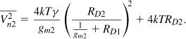
Note that the output impedance of the first stage is included in the calculation of ![]() but the noise of RD1 is not.
but the noise of RD1 is not.

Noise Figure of Lossy Circuits
Passive circuits such as filters appear at the front end of RF transceivers and their loss proves critical (Chapter 4). The loss arises from unwanted resistive components within the circuit that convert the input power to heat, thereby producing a smaller signal power at the output. Furthermore, recall from Fig. 2.37 that resistive components also generate thermal noise. That is, passive lossy circuits both attenuate the signal and introduce noise.
We wish to prove that the noise figure of a passive (reciprocal) circuit is equal to its “power loss,” defined as L = Pin/Pout, where Pin is the available source power and Pout the available power at the output. As mentioned in the derivation of Friis’ equation, the available power is the power that a given source or circuit would deliver to a conjugate-matched load. The proof is straightforward if the input and output are matched (Problem 2.20). We consider a more general case here.
Consider the arrangement shown in Fig. 2.54(a), where the lossy circuit is driven by a source impedance of RS while driving a load impedance of RL.21 From Eq. (2.130), the available source power is ![]() . To determine the available output power, we construct the Thevenin equivalent shown in Fig. 2.54(b), obtaining
. To determine the available output power, we construct the Thevenin equivalent shown in Fig. 2.54(b), obtaining ![]() . Thus, the loss is given by
. Thus, the loss is given by
![]()
Figure 2.54 (a) Lossy passive network, (b) Thevenin equivalent, (c) simplified diagram.
To calculate the noise figure, we utilize the theorem illustrated in Fig. 2.37 and the equivalent circuit shown in Fig. 2.54(c) to write
![]()
Note that RL is assumed noiseless so that only the noise figure of the lossy circuit can be determined. The voltage gain from Vin to Vout is found by noting that, in response to Vin, the circuit produces an output voltage of Vout = VThevRL/(RL + Rout) [Fig. 2.54(b)]. That is,
![]()
The NF is equal to (2.139) divided by the square of (2.140) and normalized to 4kTRS:


2.4 Sensitivity and Dynamic Range
The performance of RF receivers is characterized by many parameters. We study two, namely, sensitivity and dynamic range, here and defer the others to Chapter 3.
2.4.1 Sensitivity
The sensitivity is defined as the minimum signal level that a receiver can detect with “acceptable quality.” In the presence of excessive noise, the detected signal becomes unintelligible and carries little information. We define acceptable quality as sufficient signal-to-noise ratio, which itself depends on the type of modulation and the corruption (e.g., bit error rate) that the system can tolerate. Typical required SNR levels are in the range of 6 to 25 dB (Chapter 3).
In order to calculate the sensitivity, we write

where Psig denotes the input signal power and PRS the source resistance noise power, both per unit bandwidth. Do we express these quantities in V2/Hz or W/Hz? Since the input impedance of the receiver is typically matched to that of the antenna (Chapter 4), the antenna indeed delivers signal power and noise power to the receiver. For this reason, it is common to express both quantities in W/Hz (or dBm/Hz). It follows that
![]()
Since the overall signal power is distributed across a certain bandwidth, B, the two sides of (2.148) must be integrated over the bandwidth so as to obtain the total mean squared power. Assuming a flat spectrum for the signal and the noise, we have
![]()
Equation (2.149) expresses the sensitivity as the minimum input signal that yields a given value for the output SNR. Changing the notation slightly and expressing the quantities in dB or dBm, we have22
![]()
where Psen is the sensitivity and B is expressed in Hz. Note that (2.150) does not directly depend on the gain of the system. If the receiver is matched to the antenna, then from (2.91), PRS = kT = −174 dBm/Hz and
![]()
Note that the sum of the first three terms is the total integrated noise of the system (sometimes called the “noise floor”).
2.4.2 Dynamic Range
Dynamic range (DR) is loosely defined as the maximum input level that a receiver can “tolerate” divided by the minimum input level that it can detect (the sensitivity). This definition is quantified differently in different applications. For example, in analog circuits such as analog-to-digital converters, the DR is defined as the “full-scale” input level divided by the input level at which SNR = 1. The full scale is typically the input level beyond which a hard saturation occurs and can be easily determined by examining the circuit.
In RF design, on the other hand, the situation is more complicated. Consider a simple common-source stage. How do we define the input “full scale” for such a circuit? Is there a particular input level beyond which the circuit becomes excessively nonlinear? We may view the 1-dB compression point as such a level. But, what if the circuit senses two interferers and suffers from intermodulation?
In RF design, two definitions of DR have emerged. The first, simply called the dynamic range, refers to the maximum tolerable desired signal power divided by the minimum tolerable desired signal power (the sensitivity). Illustrated in Fig. 2.56(a), this DR is limited by compression at the upper end and noise at the lower end. For example, a cell phone coming close to a base station may receive a very large signal and must process it with acceptable distortion. In fact, the cell phone measures the signal strength and adjusts the receiver gain so as to avoid compression. Excluding interferers, this “compression-based” DR can exceed 100 dB because the upper end can be raised relatively easily.
Figure 2.56 Definitions of (a) DR and (b) SFDR.
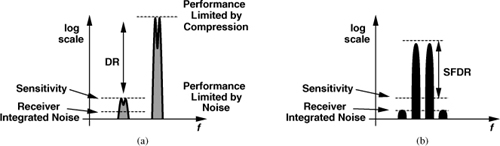
The second type, called the “spurious-free dynamic range” (SFDR), represents limitations arising from both noise and interference. The lower end is still equal to the sensitivity, but the upper end is defined as the maximum input level in a two-tone test for which the third-order IM products do not exceed the integrated noise of the receiver. As shown in Fig. 2.56(b), two (modulated or unmodulated) tones having equal amplitudes are applied and their level is raised until the IM products reach the integrated noise.23 The ratio of the power of each tone to the sensitivity yields the SFDR. The SFDR represents the maximum relative level of interferers that a receiver can tolerate while producing an acceptable signal quality from a small input level.
Where should the various levels depicted in Fig. 2.56(b) be measured, at the input of the circuit or at its output? Since the IM components appear only at the output, the output port serves as a more natural candidate for such a measurement. In this case, the sensitivity—usually an input-referred quantity—must be scaled by the gain of the circuit so that it is referred to the output. Alternatively, the output IM magnitudes can be divided by the gain so that they are referred to the input. We follow the latter approach in our SFDR calculations.
To determine the upper end of the SFDR, we rewrite Eq. (2.56) as
![]()
where, for the sake of brevity, we have denoted 20 log Ax as Px even though no actual power may be transferred at the input or output ports. Also, PIM,out represents the level of IM products at the output. If the circuit exhibits a gain of G (in dB), then we can refer the IM level to the input by writing PIM,in = PIM,out − G. Similarly, the input level of each tone is given by Pin = Pout − G. Thus, (2.152) reduces to
and hence
![]()
The upper end of the SFDR is that value of Pin which makes PIM,in equal to the integrated noise of the receiver:
![]()
The SFDR is the difference (in dB) between Pin,max and the sensitivity:
For example, a GSM receiver with NF = 7 dB, PIIP3 = − 15 dBm, and SNRmin = 12 dB achieves an SFDR of 54 dB, a substantially lower value than the dynamic range in the absence of interferers.
2.5 Passive Impedance Transformation
At radio frequencies, we often employ passive networks to transform impedances—from high to low and vice versa, or from complex to real and vice versa. Called “matching networks,” such circuits do not easily lend themselves to integration because their constituent devices, particularly inductors, suffer from loss if built on silicon chips. (We do use on-chip inductors in many RF building blocks.) Nonetheless, a basic understanding of impedance transformation is essential.
2.5.1 Quality Factor
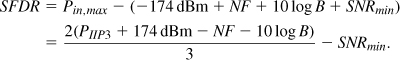
In its simplest form, the quality factor, Q, indicates how close to ideal an energy-storing device is. An ideal capacitor dissipates no energy, exhibiting an infinite Q, but a series resistance, RS [Fig. 2.57(a)], reduces its Q to

where the numerator denotes the “desired” component and the denominator, the “undesired” component. If the resistive loss in the capacitor is modeled by a parallel resistance [Fig. 2.57(b)], then we must define the Q as

because an ideal (infinite Q) results only if RP = ∞. As depicted in Figs. 2.57(c) and (d), similar concepts apply to inductors
![]()
![]()
Figure 2.57 (a) Series RC circuit, (b) equivalent parallel circuit, (c) series RL circuit, (d) equivalent parallel circuit.
While a parallel resistance appears to have no physical meaning, modeling the loss by RP proves useful in many circuits such as amplifiers and oscillators (Chapters 5 and 8). We will also introduce other definitions of Q in Chapter 8.
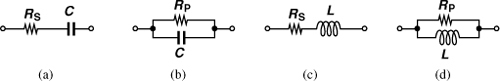
2.5.2 Series-to-Parallel Conversion
Before studying transformation techniques, let us consider the series and parallel RC sections shown in Fig. 2.58. What choice of values makes the two networks equivalent?
Figure 2.58 Series-to-parallel conversion.
Equating the impedances,
![]()
and substituting jω for s, we have
![]()
and hence
![]()
Equation (2.169) implies that QS = QP.
Of course, the two impedances cannot remain equal at all frequencies. For example, the series section approaches an open circuit at low frequencies while the parallel section does not. Nevertheless, an approximation allows equivalence for a narrow frequency range. We first substitute for RPCP in (2.169) from (2.170), obtaining
![]()
Utilizing the definition of QS in (2.163), we have
![]()
Substitution in (2.169) thus yields
![]()
So long as ![]() (which is true for a finite frequency range),
(which is true for a finite frequency range),
![]()
![]()
That is, the series-to-parallel conversion retains the value of the capacitor but raises the resistance by a factor of ![]() . These approximations for RP and CP are relatively accurate because the quality factors encountered in practice typically exceed 4. Conversely, parallel-to-series conversion reduces the resistance by a factor of
. These approximations for RP and CP are relatively accurate because the quality factors encountered in practice typically exceed 4. Conversely, parallel-to-series conversion reduces the resistance by a factor of ![]() . This statement applies to RL sections as well.
. This statement applies to RL sections as well.
2.5.3 Basic Matching Networks
A common situation in RF transmitter design is that a load resistance must be transformed to a lower value. The circuit shown in Fig. 2.59(a) accomplishes this task. As mentioned above, the capacitor in parallel with RL converts this resistance to a lower series component [Fig. 2.59(b)]. The inductance is inserted to cancel the equivalent series capacitance.
Figure 2.59 (a) Matching network, (b) equivalent circuit.

Writing Zin from Fig. 2.59(a) and replacing s with jω, we have
![]()
Thus,
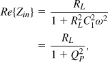
indicating that RL is transformed down by a factor of ![]() . Also, setting the imaginary part to zero gives
. Also, setting the imaginary part to zero gives
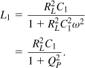
If ![]() , then
, then
The following example illustrates how the component values are chosen.
Solution:
Assuming ![]() , we have from Eqs. (2.181) and (2.182), C1 = 0.90 pF and L1 = 1.13 nH, respectively. Unfortunately, however, QP = 1.41, indicating that Eqs. (2.178) and (2.180) must be used instead. We thus obtain C1 = 0.637 pF and L1 = 0.796 nH.
, we have from Eqs. (2.181) and (2.182), C1 = 0.90 pF and L1 = 1.13 nH, respectively. Unfortunately, however, QP = 1.41, indicating that Eqs. (2.178) and (2.180) must be used instead. We thus obtain C1 = 0.637 pF and L1 = 0.796 nH.
In order to transform a resistance to a higher value, the capacitive network shown in Fig. 2.60(a) can be used. The series-parallel conversion results derived previously provide insight here. If Q2 ![]() 1, the parallel combination of C1 and RL can be converted to a series network [Fig. 2.60(b)], where RS ≈ [RL(C1ω)2]−1 and CS ≈ C1. Viewing C2 and C1 as one capacitor, Ceq, and converting the resulting series section to a parallel circuit [Fig. 2.60(c)], we have
1, the parallel combination of C1 and RL can be converted to a series network [Fig. 2.60(b)], where RS ≈ [RL(C1ω)2]−1 and CS ≈ C1. Viewing C2 and C1 as one capacitor, Ceq, and converting the resulting series section to a parallel circuit [Fig. 2.60(c)], we have

Figure 2.60 (a) Capacitive matching circuit, (b) simplified circuit with parallel-to-series conversion, (c) simplified circuit with series-to-parallel conversion.
That is, the network “boosts” the value of RL by a factor of (1 + C1/C2)2. Also,
![]()
Note that the capacitive component must be cancelled by placing an inductor in parallel with the input.
For low Q values, the above derivations incur significant error. We thus compute the input admittance (1/Yin) and replace s with jω,
![]()
The real part of Yin yields the equivalent resistance seen to ground if we write

In comparison with Eq. (2.184), this result contains an additional component, ![]() .
.
Figure 2.61 (a) Matching network, (b) simplified circuit.
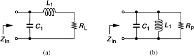
Solution:
We postulate that conversion of the L1–RL branch to a parallel section produces a higher resistance. If ![]() , then the equivalent parallel resistance is obtained from Eq. (2.174) as
, then the equivalent parallel resistance is obtained from Eq. (2.174) as

The intuition gained from our analysis of matching networks leads to the four “L-section” topologies24 shown in Fig. 2.62. In Fig. 2.62(a), C1 transforms RL to a smaller series value and L1 cancels C1. Similarly, in Fig. 2.62(b), L1 transforms RL to a smaller series value while C1 resonates with L1. In Fig. 2.62(c), L1 transforms RL to a larger parallel value and C1 cancels the resulting parallel inductance. A similar observation applies to Fig. 2.62(d).
Figure 2.62 Four L sections used for matching.
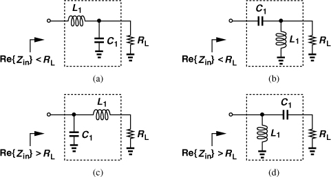
How do these networks transform voltages and currents? As an example, consider the circuit in Fig. 2.62(a). For a sinusoidal input voltage with an rms value of Vin, the power delivered to the input port is equal to ![]() , and that delivered to the load,
, and that delivered to the load, ![]() . If L1 and C1 are ideal, these two powers must be equal, yielding
. If L1 and C1 are ideal, these two powers must be equal, yielding

This result, of course, applies to any lossless matching network whose input impedance contains a zero imaginary part. Since Pin = VinIin and Pout = VoutIout, we also have
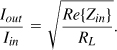
For example, a network transforming RL to a lower value “amplifies” the voltage and attenuates the current by the above factor.
Solution:
![]()
Figure 2.63 (a) Input and (b) output impedances of a lossless passive network.


pointing to the Thevenin equivalent shown in Fig. 2.63(b). We observe that the network transforms RS by a factor of 1/α and the input voltage by a factor of ![]() , similar to that in Eq. (2.191). In other words, if the input and output ports of such a network are swapped, the resistance transformation ratio is simply inverted.
, similar to that in Eq. (2.191). In other words, if the input and output ports of such a network are swapped, the resistance transformation ratio is simply inverted.
Transformers can also transform impedances. An ideal transformer having a turns ratio of n “amplifies” the input voltage by a factor of n (Fig. 2.64). Since no power is lost, ![]() and hence Rin = RL/n2. The behavior of actual transformers, especially those fabricated monolithically, is studied in Chapter 7.
and hence Rin = RL/n2. The behavior of actual transformers, especially those fabricated monolithically, is studied in Chapter 7.
Figure 2.64 Impedance transformation by a physical transformer.

The networks studied here operate across only a narrow bandwidth because the transformation ratio, e.g., 1 + Q2, varies with frequency, and the capacitance and inductance approximately resonate over a narrow frequency range. Broadband matching networks can be constructed, but they typically suffer from a high loss.
2.5.4 Loss in Matching Networks
Our study of matching networks has thus far neglected the loss of their constituent components, particularly, that of inductors. We analyze the effect of loss in a few cases here, but, in general, simulations are necessary to determine the behavior of complex lossy networks.
Consider the matching network of Fig. 2.62(a), shown in Fig. 2.65 with the loss of L1 modeled by a series resistance, RS. We define the loss as the power provided by the input divided by that delivered to RL. The former is equal to
![]()
and the latter,
![]()
because the power delivered to Rin1 is entirely absorbed by RL. It follows that
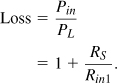
Figure 2.65 Lossy matching network with series resistence.
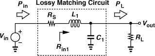
For example, if RS = 0.1 Rin1, then the (power) loss reaches 0.41 dB. Note that this network transforms RL to a lower value, ![]() , thereby suffering from loss even if RS appears small.
, thereby suffering from loss even if RS appears small.
As another example, consider the network of Fig. 2.62(b), depicted in Fig. 2.66 with the loss of L1 modeled by a parallel resistance, RP. We note that the power delivered by Vin, Pin, is entirely absorbed by RP||RL:

Figure 2.66 Lossy matching network with parallel resistence.
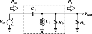
Recognizing ![]() as the power delivered to the load, PL, we have
as the power delivered to the load, PL, we have
![]()
For example, if RP = 10RL, then the loss is equal to 0.41 dB.
2.6 Scattering Parameters
Microwave theory deals mostly with power quantities rather than voltage or current quantities. Two reasons can explain this approach. First, traditional microwave design is based on transfer of power from one stage to the next. Second, the measurement of high-frequency voltages and currents in the laboratory proves very difficult, whereas that of average power is more straightforward. Microwave theory therefore models devices, circuits, and systems by parameters that can be obtained through the measurement of power quantities. They are called “scattering parameters” (S-parameters).
Before studying S-parameters, we introduce an example that provides a useful viewpoint. Consider the L1–C1 series combination depicted in Fig. 2.67. The circuit is driven by a sinusoidal source, Vin, having an output impedance of RS. A load resistance of RL = RS is tied to the output port. At an input frequency of ![]() , L1 and C1 form a short circuit, providing a conjugate match between the source and the load. In analogy with transmission lines, we say the “incident wave” produced by the signal source is absorbed by RL. At other frequencies, however, L1 and C1 attenuate the voltage delivered to RL. Equivalently, we say the input port of the circuit generates a “reflected wave” that returns to the source. In other words, the difference between the incident power (the power that would be delivered to a matched load) and the reflected power represents the power delivered to the circuit.
, L1 and C1 form a short circuit, providing a conjugate match between the source and the load. In analogy with transmission lines, we say the “incident wave” produced by the signal source is absorbed by RL. At other frequencies, however, L1 and C1 attenuate the voltage delivered to RL. Equivalently, we say the input port of the circuit generates a “reflected wave” that returns to the source. In other words, the difference between the incident power (the power that would be delivered to a matched load) and the reflected power represents the power delivered to the circuit.
Figure 2.67 Incident wave in a network.
The above viewpoint can be generalized for any two-port network. As illustrated in Fig. 2.68, we denote the incident and reflected waves at the input port by ![]() and
and ![]() , respectively. Similar waves are denoted by
, respectively. Similar waves are denoted by ![]() and
and ![]() , respectively, at the output. Note that
, respectively, at the output. Note that ![]() denotes a wave generated by Vin as if the input impedance of the circuit were equal to RS. Since that may not be the case, we include the reflected wave,
denotes a wave generated by Vin as if the input impedance of the circuit were equal to RS. Since that may not be the case, we include the reflected wave, ![]() , so that the actual voltage measured at the input is equal to
, so that the actual voltage measured at the input is equal to ![]() +
+ ![]() . Also,
. Also, ![]() denotes the incident wave traveling into the output port or, equivalently, the wave reflected from RL. These four quantities are uniquely related to one another through the S-parameters of the network:
denotes the incident wave traveling into the output port or, equivalently, the wave reflected from RL. These four quantities are uniquely related to one another through the S-parameters of the network:
![]()
![]()
Figure 2.68 Illustration of incident and reflected waves at the input and output.
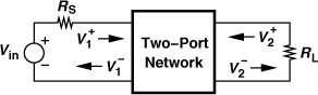
With the aid of Fig. 2.69, we offer an intuitive interpretation for each parameter:
1. For S11, we have from Fig. 2.69(a)
![]()
Thus, S11 is the ratio of the reflected and incident waves at the input port when the reflection from RL (i.e., ![]() ) is zero. This parameter represents the accuracy of the input matching.
) is zero. This parameter represents the accuracy of the input matching.
2. For S12, we have from Fig. 2.69(b)
![]()
Thus, S12 is the ratio of the reflected wave at the input port to the incident wave into the output port when the input port is matched. In this case, the output port is driven by the signal source. This parameter characterizes the “reverse isolation” of the circuit, i.e., how much of the output signal couples to the input network.
3. For S22, we have from Fig. 2.69(c)
![]()
Thus, S22 is the ratio of reflected and incident waves at the output when the reflection from RS (i.e., ![]() ) is zero. This parameter represents the accuracy of the output matching.
) is zero. This parameter represents the accuracy of the output matching.
4. For S21, we have from Fig. 2.69(d)
![]()
Figure 2.69 Illustration of four S-parameters.
Thus, S21 is the ratio of the wave incident on the load to that going to the input when the reflection from RL is zero. This parameter represents the gain of the circuit.
We should make a few remarks at this point. First, S-parameters generally have frequency-dependent complex values. Second, we often express S-parameters in units of dB as follows
![]()
Third, the condition ![]() in Eqs. (2.204) and (2.207) requires that the reflection from RL be zero, but it does not mean that the output port of the circuit must be conjugate-matched to RL. This condition simply means that if, hypothetically, a transmission line having a characteristic impedance equal to RS carries the output signal to RL, then no wave is reflected from RL. A similar note applies to the requirement
in Eqs. (2.204) and (2.207) requires that the reflection from RL be zero, but it does not mean that the output port of the circuit must be conjugate-matched to RL. This condition simply means that if, hypothetically, a transmission line having a characteristic impedance equal to RS carries the output signal to RL, then no wave is reflected from RL. A similar note applies to the requirement ![]() in Eqs. (2.205) and (2.206). The conditions
in Eqs. (2.205) and (2.206). The conditions ![]() at the input or
at the input or ![]() at the output facilitate high-frequency measurements while creating issues in modern RF design. As mentioned in Section 2.3.5 and exemplified by the cascade of stages in Fig. 2.53, modern RF design typically does not strive for matching between stages. Thus, if S11 of the first stage must be measured with RL = RS at its output, then its value may not represent the S11 of the cascade.
at the output facilitate high-frequency measurements while creating issues in modern RF design. As mentioned in Section 2.3.5 and exemplified by the cascade of stages in Fig. 2.53, modern RF design typically does not strive for matching between stages. Thus, if S11 of the first stage must be measured with RL = RS at its output, then its value may not represent the S11 of the cascade.
In modern RF design, S11 is the most commonly-used S parameter as it quantifies the accuracy of impedance matching at the input of receivers. Consider the arrangement shown in Fig. 2.70, where the receiver exhibits an input impedance of Zin. The incident wave ![]() is given by Vin/2 (as if Zin were equal to RS). Moreover, the total voltage at the receiver input is equal to VinZin/(Zin + RS), which is also equal to
is given by Vin/2 (as if Zin were equal to RS). Moreover, the total voltage at the receiver input is equal to VinZin/(Zin + RS), which is also equal to ![]() . Thus,
. Thus,
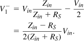
Figure 2.70 Receiver with incident and reflected waves.
It follows that
![]()
Called the “input reflection coefficient” and denoted by Γin, this quantity can also be considered to be S11 if we remove the condition ![]() in Eq. (2.204).
in Eq. (2.204).
Figure 2.71 (a) CG stage for calculation of S-parameters, (b) inclusion of capacitors, (c) effect of reflected wave at output.
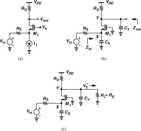
Solution:
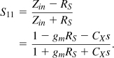
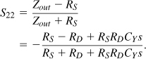
Lastly, S21 is obtained according to the configuration of Fig. 2.71(c). Since ![]() ,
, ![]() , and VX/Vin = Zin/(Zin + RS), we obtain
, and VX/Vin = Zin/(Zin + RS), we obtain
![]()
![]()
2.7 Analysis of Nonlinear Dynamic Systems25
In our treatment of systems in Section 2.2, we have assumed a static nonlinearity, e.g., in the form of y(t) = α1x(t) + α2x2(t) + α3x3(t). In some cases, a circuit may exhibit dynamic nonlinearity, requiring a more complex analysis. In this section, we address this task.
2.7.1 Basic Considerations
Let us first consider a general nonlinear system with an input given by x(t) = A1 cos ω1t + A2 cos ω2t. We expect the output, y(t), to contain harmonics at nω1, mω2, and IM products at kω1 ± qω2, where, n, m, k, and q are integers. In other words,

In the above equation, an, bn, cm,n, and the phase shifts are frequency-dependent quantities. If the differential equation governing the system is known, we can simply substitute for y(t) from this expression, equate the like terms, and compute an, bn, cm,n, and the phase shifts. For example, consider the simple RC section shown in Fig. 2.72, where the capacitor is nonlinear and expressed as C1 = C0(1 + αVout). Adding the voltages across R1 and C1 and equating the result to Vin, we have
![]()
Figure 2.72 RC circuit with nonlinear capacitor.

Now suppose Vin(t) = V0 cos ω1t+V0 cos ω2t (as in a two-tone test) and assume the system is only “weakly” nonlinear, i.e., only the output terms at ω1, ω2, ω1 ± ω2, 2ω1 ± ω2, and 2ω2 ± ω1 are significant. Thus, the output assumes the form
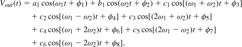
where, for simplicity, we have used cm and φm. We must now substitute for Vout(t) and Vin(t) in (2.219), convert products of sinusoids to sums, bring all of the terms to one side of the equation, group them according to their frequencies, and equate the coefficient of each sinusoid to zero. We thus obtain a system of 16 nonlinear equations and 16 knowns (a1, b1, c1, ..., c6, φ1, ..., φ8).
This type of analysis is called “harmonic balance” because it predicts the output frequencies and attempts to “balance” the two sides of the circuit’s differential equation by including these components in Vout(t). The mathematical labor in harmonic balance makes hand analysis difficult or impossible. The “Volterra series” approach, on the other hand, prescribes a recursive method that computes the response more accurately in successive steps without the need for solving nonlinear equations. A detailed treatment of the concepts described below can be found in [10–14].
2.8 Volterra Series
In order to understand how the Volterra series represents the time response of a system, we begin with a simple input form, Vin(t) = V0 exp(jω1t). Of course, if we wish to obtain the response to a sinusoid of the form V0 cos ω1t = Re{V0 exp(jω1t)}, we simply calculate the real part of the output.26 (The use of the exponential form greatly simplifies the manipulation of the product terms.) For a linear, time-invariant system, the output is given by
![]()
where H(ω1) is the Fourier transform of the impulse response. For example, if the capacitor in Fig. 2.72 is linear, i.e., C1 = C0, then we can substitute for Vout and Vin in Eq. (2.219):
![]()
It follows that
![]()
Note that the phase shift introduced by the circuit is included in H(ω1) here.
As our next step, let us ask, how should the output response of a dynamic nonlinear system be expressed? To this end, we apply two tones to the input, Vin(t) = V0 exp(jω1t) + V0 exp(jω2t), recognizing that the output consists of both linear and nonlinear responses. The former are of the form
![]()
and the latter include exponentials such as exp[j(ω1 + ω2)t], etc. We expect that the coefficient of such an exponential is a function of both ω1 and ω2. We thus make a slight change in our notation: we denote H(ωj) in Eq. (2.224) by H1(ωj) [to indicate first-order (linear) terms] and the coefficient of exp[j(ω1 + ω2)t] by H2(ω1, ω2). In other words, the overall output can be written as
![]()
How do we determine the terms at 2ω1, 2ω2, and ω1 − ω2? If H2(ω1, ω2) exp[j(ω1 + ω2)t] represents the component at ω1 + ω2, then H2(ω1, ω1) exp[j(2ω1)t] must model that at 2ω1. Similarly, H2(ω2, ω2) and H2(ω1, −ω2) serve as coefficients for exp[j(2ω2)t] and exp[j(ω1 − ω2)t], respectively. In other words, a more complete form of Eq. (2.225) reads
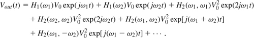
Thus, our task is simply to compute H2(ω1, ω2).
Solution:
We apply the input Vin(t) = V0 exp(jω1t) + V0 exp(jω2t) and assume the output is of the form ![]() . We substitute for Vout and Vin in Eq. (2.219):
. We substitute for Vout and Vin in Eq. (2.219):


![]()
![]()
Why did we assume ![]() while we know that Vout(t) also contains terms at 2ω1, 2ω2, and ω1 − ω2? This is because these other exponentials do not yield terms of the form exp[j(ω1 + ω2)t].
while we know that Vout(t) also contains terms at 2ω1, 2ω2, and ω1 − ω2? This is because these other exponentials do not yield terms of the form exp[j(ω1 + ω2)t].
Solution:
As mentioned earlier, the component at 2ω1 is obtained as ![]() . Thus, the amplitude is equal to
. Thus, the amplitude is equal to
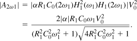
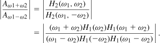

The foregoing examples point to a methodical approach that allows us to compute the second harmonic or second-order IM components with a moderate amount of algebra. But how about higher-order harmonics or IM products? We surmise that for Nth-order terms, we must apply the input Vin(t) = V0 exp(jω1t) + ... + V0 exp(jωNt) and compute Hn(ω1,..., ωn) as the coefficient of the exp[j(ω1 + ... + ωn)t] terms in the output. The output can therefore be expressed as
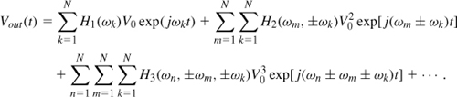
The above representation of the output is called the Volterra series. As exemplified by (2.230), Hm(ω1, ..., ωm) can be computed in terms of H1, ..., Hm−1 with no need to solve nonlinear equations. We call Hm the m-th “Volterra kernel.”
Solution:
We assume Vin(t) = V0 exp(jω1t) + V0 exp(jω2t) + V0 exp(jω3t). Since the output contains many components, we introduce the short hands H1(1) = H1(ω1)V0 exp(jω1t), H1(2) = H1(ω2)V0 exp(jω2t), etc., ![]() , etc., and
, etc., and ![]() . We express the output as
. We express the output as
![]()
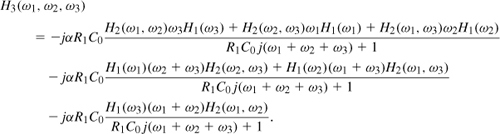
The reader may wonder if the Volterra series can be used with inputs other than exponentials. This is indeed possible [14] but beyond the scope of this book.
The approach described in this section is called the “harmonic” method of kernel calculation. In summary, this method proceeds as follows:
1. Assume Vin(t) = V0 exp(jω1t) and Vout(t) = H1(ω1)V0 exp(jω1t). Substitute for Vout and Vin in the system’s differential equation, group the terms that contain exp(jω1t), and compute the first (linear) kernel, H1(ω1).
2. Assume Vin(t) = V0 exp(jω1t)+V0 exp(jω2t) and ![]() . Make substitutions in the differential equation, group the terms that contain exp[j(ω1 + ω2)t], and determine the second kernel, H2(ω1, ω2).
. Make substitutions in the differential equation, group the terms that contain exp[j(ω1 + ω2)t], and determine the second kernel, H2(ω1, ω2).
3. Assume Vin(t) = V0 exp(jω1t) + V0 exp(jω2t) + V0 exp(jω3t) and Vout(t) is given by Eq. (2.237). Make substitutions, group the terms that contain exp[j(ω1 + ω2 + ω3)t], and calculate the third kernel, H3(ω1, ω2, ω3).
4. To compute the amplitude of harmonics and IM components, choose ω1, ω2, ... properly. For example, H2(ω1, ω1) yields the transfer function for 2ω1 and H3(ω1, −ω2, ω1) the transfer function for 2ω1 − ω2.
2.8.1 Method of Nonlinear Currents
As seen in Example 2.34, the harmonic method becomes rapidly more complex as n increases. An alternative approach called the method of “nonlinear currents” is sometimes preferred as it reduces the algebra to some extent. We describe the method itself here and refer the reader to [13] for a formal proof of its validity.
The method of nonlinear currents proceeds as follows for a circuit that contains a two-terminal nonlinear device [13]:
1. Assume Vin(t) = V0 exp(jω1t) and determine the linear response of the circuit by ignoring the nonlinearity. The “response” includes both the output of interest and the voltage across the nonlinear device.
2. Assume Vin(t) = V0 exp(jω1t) + V0 exp(jω2t) and calculate the voltage across the nonlinear device, assuming it is linear. Now, compute the nonlinear component of the current flowing through the device, assuming the device is nonlinear.
3. Set the main input to zero and place a current source equal to the nonlinear component found in Step 2 in parallel with the nonlinear device.
4. Ignoring the nonlinearity of the device again, determine the circuit’s response to the current source applied in Step 3. Again, the response includes the output of interest and the voltage across the nonlinear device.
5. Repeat Steps 2, 3, and 4 for higher-order responses. The overall response is equal to the output components found in Steps 1, 4, etc.
The following example illustrates the procedure.
Solution:
![]()
![]()
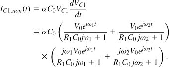

Figure 2.73 Inclusion of nonlinear current in RC section.
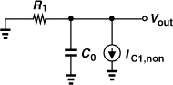
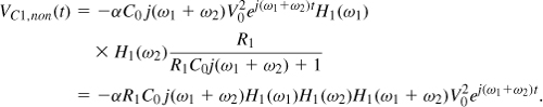
We note that the coefficient of ![]() in these two equations is the same as H2(ω1, ω2) in (2.229).
in these two equations is the same as H2(ω1, ω2) in (2.229).
![]()
![]()
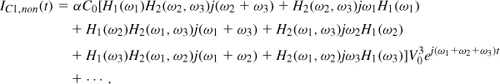
The procedure described above applies to two-terminal nonlinear devices. For transistors, a similar approach can be taken. We illustrate this point with the aid of an example.
Figure 2.74 (a) CS stage with inductors in series with source and gate, (b) inclusion of nonlinear current, (c) computation of output current.

Solution:
![]()
![]()

where ![]() . Note that Iout = gmV1 = gmH1(ω)Vin.
. Note that Iout = gmV1 = gmH1(ω)Vin.
![]()
Upon experiencing the characteristic ![]() , this voltage results in a nonlinear current given by
, this voltage results in a nonlinear current given by
![]()
![]()
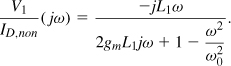
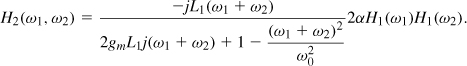
![]()
Since ![]() , the nonlinear current at ω1 + ω2 + ω3 is expressed as
, the nonlinear current at ω1 + ω2 + ω3 is expressed as
References
[1] B. Razavi, Design of Analog CMOS Integrated Circuits, Boston: McGraw-Hill, 2001.
[2] L. W. Couch, Digital and Analog Communication Systems, Fourth Edition, New York: Macmillan Co., 1993.
[3] A. van der Ziel, “Thermal Noise in Field Effect Transistors,” Proc. IRE, vol. 50, pp. 1808–1812, Aug. 1962.
[4] A. A. Abidi, “High-Frequency Noise Measurements on FETs with Small Dimensions,” IEEE Trans. Electron Devices, vol. 33, pp. 1801–1805, Nov. 1986.
[5] A. J. Sholten et al., “Accurate Thermal Noise Model of Deep-Submicron CMOS,” IEDM Dig. Tech. Papers, pp. 155–158, Dec. 1999.
[6] B. Razavi, “Impact of Distributed Gate Resistance on the Performance of MOS Devices,” IEEE Trans. Circuits and Systems-Part I, vol. 41, pp. 750–754, Nov. 1994.
[7] H. T. Friis, “Noise Figure of Radio Receivers,” Proc. IRE, vol. 32, pp. 419–422, July 1944.
[8] A. Papoulis, Probability, Random Variables, and Stochastic Processes, Third Edition, New York: McGraw-Hill, 1991.
[9] R. W. Bennet, “Methods of Solving Noise Problems,” Proc. IRE, vol. 44, pp. 609–638, May 1956.
[10] S. Narayanan, “Application of Volterra Series to Intermodulation Distortion Analysis of Transistor Feedback Amplifiers,” IEEE Tran. Circuit Theory, vol. 17, pp. 518–527, Nov. 1970.
[11] P. Wambacq et al., “High-Frequency Distortion Analysis of Analog Integrated Circuits,” IEEE Tran. Circuits and Systems, II, vol. 46, pp. 335–334, March 1999.
[12] P. Wambaq and W. Sansen, Distortion Analysis of Analog Integrated Circuits, Norwell, MA: Kluwer, 1998.
[13] J. Bussganag, L. Ehrman, and J. W. Graham, “Analysis of Nonlinear Systems with Multiple Inputs,” Proc. IEEE, vol. 62, pp. 1088–1119, Aug. 1974.
[14] E. Bedrosian and S. O. Rice, “The Output Properties of Volterra Systems (Nonlinear Systems with Memory) Driven by Harmonic and Gaussian Inputs,” Proc. IEEE, vol. 59, pp. 1688–1707, Dec. 1971.
Problems
2.1. Two nonlinear stages are cascaded. If the input/output characteristic of each stage is approximated by a third-order polynomial, determine the P1dB of the cascade in terms of the P1dB of each stage.
2.2. Repeat Example 2.11 if one interferer has a level of −3 dBm and the other, −35 dBm.
2.3. If cascaded, stages having only second-order nonlinearity can yield a finite IP3. For example, consider the cascade identical common-source stages shown in Fig. 2.75.
Figure 2.75 Cascade of CS stages.
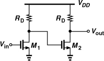
If each transistor operates in saturation and follows the ideal square-law behavior, determine the IP3 of the cascade.
2.4. Determine the IP3 and P1dB for a system whose characteristic is approximated by a fifth-order polynomial.
2.5. Consider the scenario shown in Fig. 2.76, where ω3 − ω2 = ω2 − ω3 and the bandpass filter provides an attenuation of 17 dB at ω2 and 37 dB at ω3.
Figure 2.76 Cascade of BPF and amplifier.
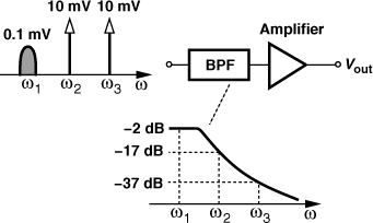
(a) Compute the IIP3 of the amplifier such that the intermodulation product falling at ω1 is 20 dB below the desired signal.
(b) Suppose an amplifier with a voltage gain of 10 dB and IIP3 = 500 mVp precedes the band-pass filter. Calculate the IIP3 of the overall chain. (Neglect second-order nonlinearities.)
2.6. Prove that the Fourier transform of the autocorrelation of a random signal yields the spectrum, i.e., the power measured in a 1-Hz bandwidth at each frequency.
2.7. A broadband circuit sensing an input V0 cos ω0t produces a third harmonic V3 cos(3ω0t). Determine the 1-dB compression point in terms of V0 and V3.
2.8. Prove that in Fig. 2.36, the noise power delivered by R1 to R2 is equal to that delivered by R2 to R1 if the resistors reside at the same temperature. What happens if they do not?
2.9. Explain why the channel thermal noise of a MOSFET is modeled by a current source tied between the source and drain terminals (rather than, say, between the gate and source terminals).
2.10. Prove that the channel thermal noise of a MOSFET can be referred to the gate as a voltage given by 4kTγ/gm. As shown in Fig. 2.77, the two circuits must generate the same current with the same terminal voltages.
Figure 2.77 Equivalent circuits for noise of a MOSFET.

2.11. Determine the NF of the circuit shown in Fig. 2.52 using Friis’ equation.
2.12. Prove that the output noise voltage of the circuit shown in Fig. 2.46(c) is given by ![]() .
.
2.13. Repeat Example 2.23 if the CS and CG stages are swapped. Does the NF change? Why?
2.14. Repeat Example 2.23 if RD1 and RD2 are replaced with ideal current sources and channel-length modulation is not neglected.
2.15. The input/output characteristic of a bipolar differential pair is given by Vout = −2RCIEE tanh[Vin/(2VT)], where RC denotes the load resistance, IEE is the tail current, and VT = kT/q. Determine the IP3 of the circuit.
2.16. What happens to the noise figure of a circuit if the circuit is loaded by a noiseless impedance ZL at its output?
2.17. The noise figure of a circuit is known for a source impedance of RS1. Is it possible to compute the noise figure for another source impedance RS2? Explain in detail.
2.18. Equation (2.122) implies that the noise figure falls as RS rises. Assuming that the antenna voltage swing remains constant, explain what happens to the output SNR as RS increases.
2.19. Repeat Example 2.21 for the arrangement shown in Fig. 2.78, where the transformer amplifies its primary voltage by a factor of n and transforms RS to a value of n2RS.
Figure 2.78 CS stage driven by a transformer.
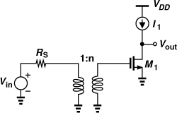
2.20. For matched inputs and outputs, prove that the NF of a passive (reciprocal) circuit is equal to its power loss.
2.21. Determine the noise figure of each circuit in Fig. 2.79 with respect to a source impedance RS. Neglect channel-length modulation and body effect.
Figure 2.79 CS stages for NF calculation.
2.22. Determine the noise figure of each circuit in Fig. 2.80 with respect to a source impedance RS. Neglect channel-length modulation and body effect.
Figure 2.80 CG stages for NF calculation.
2.23. Determine the noise figure of each circuit in Fig. 2.81 with respect to a source impedance RS. Neglect channel-length modulation and body effect.
Figure 2.81 Stages for NF calculation.