Chapter 8. Oscillators
In our study of RF transceivers in Chapter 4, we noted the extensive use of oscillators in both the transmit and receive paths. Interestingly, in most systems, one input of every mixer is driven by a periodic signal, hence the need for oscillators. This chapter deals with the analysis and design of oscillators. The outline is shown below.

8.1 Performance Parameters
An oscillator used in an RF transceiver must satisfy two sets of requirements: (1) system specifications, e.g., the frequency of operation and the “purity” of the output, and (2) “interface” specifications, e.g., drive capability or output swing. In this section, we study the oscillator performance parameters and their role in the overall system.
Frequency Range
An RF oscillator must be designed such that its frequency can be varied (tuned) across a certain range. This range includes two components: (1) the system specification; for example, a 900-MHz GSM direct-conversion receiver may tune the LO from 935 MHz to 960 MHz; (2) additional margin to cover process and temperature variations and errors due to modeling inaccuracies. The latter component typically amounts to several percent.
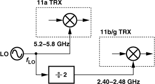
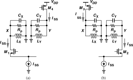
The actual frequency range of an oscillator may also depend on whether quadrature outputs are required and/or injection pulling is of concern (Chapter 4). A direct-conversion transceiver employs quadrature phases of the carrier, necessitating that either the oscillator directly generate quadrature outputs or it run at twice the required frequency so that a ÷2 stage can produce such outputs. For example, in the hybrid topology of Fig. 8.1, the LO must still provide quadrature phases in the 5-GHz range—but it is prone to injection pulling by the PA output. We address the problem of quadrature generation in Section 8.11.
How high a frequency can one expect of a CMOS oscillator? While oscillation frequencies as high as 300 GHz have been demonstrated [1], in practice, a number of serious trade-offs emerge that become much more pronounced at higher operation frequencies. We analyze these trade-offs later in this chapter.
Output Voltage Swing
As exemplified by the arrangement shown in Fig. 8.1, the oscillators in an RF system drive mixers and frequency dividers. As such, they must produce sufficiently large output swings to ensure nearly complete switching of the transistors in the subsequent stages. Furthermore, as studied in Section 8.7, excessively low output swings exacerbate the effect of the internal noise of the oscillator. With a 1-V supply, a typical single-ended swing may be around 0.6 to 0.8 Vpp. A buffer may follow the oscillator to amplify the swings and/or drive the subsequent stage.
Drive Capability
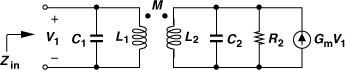
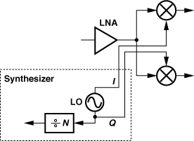
Oscillators may need to drive a large load capacitance. Figure 8.2 depicts a typical arrangement for the receive path. In addition to the downconversion mixers, the oscillator must also drive a frequency divider, denoted by a ÷N block. This is because a loop called the “frequency synthesizer” must precisely control the frequency of the oscillator, requiring a divider (Chapter 10). In other words, the LO must drive the input capacitance of at least one mixer and one divider.
Figure 8.2 Circuits loading the LO.
Interestingly, typical mixers and dividers exhibit a trade-off between the minimum LO swing with which they can operate properly and the capacitance that they present at their LO port. This can be seen in the representative stage shown in Fig. 8.3(a), wherein it is desirable to switch M1 and M2 as abruptly as possible (Chapter 6). To this end, we can select large LO swings so that VGS1 − VGS2 rapidly reaches a large value, turning off one transistor [Fig. 8.3(b)]. Alternatively, we can employ smaller LO swings but wider transistors so that they steer their current with a smaller differential input.
Figure 8.3 (a) Representative LO path of mixers and dividers, (b) current-steering with large LO swings, (c) current-steering with small LO swings but wide transistors.

The issue of capacitive loading becomes more serious in transmitters. As explained in Example 6.37, the PA input capacitance “propagates” to the LO port of the upconversion mixers.
To alleviate the loading presented by mixers and dividers and perhaps amplify the swings, we can follow the LO with a buffer, e.g., a differential pair. Note that in Fig. 8.2, two buffers are necessary for the quadrature phases. The buffers consume additional power and may require inductive loads—owing to speed limitations or the need for swings above the supply voltage (Chapter 6). The additional inductors complicate the layout and the routing of the high-frequency signals.
Solution:
![]()
Figure 8.4 Input admittance of differential pair.
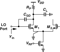
![]()
It is also reasonable to assume that CL ![]() CGD in a downconversion mixer, arriving at the following parallel resistive component seen at the input:
CGD in a downconversion mixer, arriving at the following parallel resistive component seen at the input:
![]()
Phase Noise
The spectrum of an oscillator in practice deviates from an impulse and is “broadened” by the noise of its constituent devices. Called “phase noise,” this phenomenon has a profound effect on RF receivers and transmitters (Section 8.7). Unfortunately, phase noise bears direct trade-offs with the tuning range and power dissipation of oscillators, making the design more challenging. Since the phase noise of LC oscillators is inversely proportional to the Q of their tank(s), we will pay particular attention to factors that degrade the Q.
Output Waveform
What is the desired output waveform of an RF oscillator? Recall from the analysis of mixers in Chapter 6 that abrupt LO transitions reduce the noise and increase the conversion gain. Moreover, effects such as direct feedthrough are suppressed if the LO signal has a 50% duty cycle. Sharp transitions also improve the performance of frequency dividers (Chapter 10). Thus, the ideal LO waveform in most cases is a square wave.
In practice, it is difficult to generate square LO waveforms. This is primarily because the LO circuitry itself and the buffer(s) following it typically incorporate (narrowband) resonant loads, thereby attenuating the harmonics. For this reason, as illustrated in Fig. 8.3, the LO amplitude is chosen large and/or the switching transistors wide so as to approximate abrupt current switching.
A number of considerations call for differential LO waveforms. First, as observed in Chapter 6, balanced mixers outperform unbalanced topologies in terms of gain, noise, and dc offsets. Second, the leakage of the LO to the input is generally smaller with differential waveforms.
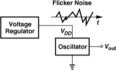
Supply Sensitivity
The frequency of an oscillator may vary with the supply voltage, an undesirable effect because it translates supply noise to frequency (and phase) noise. For example, external or internal voltage regulators may suffer from substantial flicker noise, which cannot be easily removed by bypass capacitors due to its low-frequency contents. This noise therefore modulates the oscillation frequency (Fig. 8.5).
Figure 8.5 Effect of regulator noise on an oscillator.
Power Dissipation
The power drained by the LO and its buffer(s) proves critical in some applications as it trades with the phase noise and tuning range. Thus, many techniques have been introduced that lower the phase noise for a given power dissipation.
8.2 Basic Principles
An oscillator generates a periodic output. As such, the circuit must involve a self-sustaining mechanism that allows its own noise to grow and eventually become a periodic signal.
8.2.1 Feedback View of Oscillators
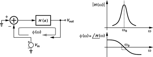
An oscillator may be viewed as a “badly-designed” negative-feedback amplifier—so badly-designed that it has a zero or negative phase margin. While the art of oscillator design entails much more than an unstable amplifier, this view provides a good starting point for our study. Consider the simple linear negative-feedback system depicted in Fig. 8.6, where
![]()
Figure 8.6 Negative feedback system.
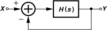
What happens if at a sinusoidal frequency, ω1, H(s = jω1) becomes equal to −1? The gain from the input to the output goes to infinity, allowing the circuit to amplify a noise component at ω1 indefinitely. That is, the circuit can sustain an output at ω1. From another point of view, the closed-loop system exhibits two imaginary poles given by ±jω1.

The above example leads to a general and powerful analytical point: in the small-signal model of an oscillator, the impedance seen between any two nodes (one of which is not ground) in the signal path goes to infinity at the oscillation frequency, ω1, because a noise current at ω1 injected between these two nodes produces an infinitely large swing. This observation can be used to determine the oscillation condition and frequency.
Since H(s) is a complex function, the condition H(jω1) = −1 can equivalently be expressed as
![]()
![]()
which are called “Barkhausen’s criteria” for oscillation. Let us examine these two conditions to develop more insight. We recognize that a signal at ω1 experiences a gain of unity and a phase shift of 180° as it travels through H(s) [Fig. 8.8(a)]. Bearing in mind that the system is originally designed to have negative feedback (as denoted by the input subtractor), we conclude that the signal at ω1 experiences a total phase shift of 360° [Fig. 8.8(b)] as it travels around the loop. This is, of course, to be expected: for the circuit to reach steady state, the signal returning to A must exactly coincide with the signal that started at A. We call ∠H(jω1) a “frequency-dependent” phase shift to distinguish it from the 180° phase due to negative feedback.
Figure 8.8 Barkhausen’s phase shift criterion viewed as (a) 180° frequency-dependent phase shift due to H(s), (b) 360° total phase shift.

The above point can also be viewed as follows. Even though the system was originally configured to have negative feedback, H(s) is so “sluggish” that it contributes an additional phase shift of 180° at ω1, thereby creating positive feedback at this frequency.
What is the significance of |H(jω1)| = 1? For a noise component at ω1 to “build up” as it circulates around the loop with positive feedback, the loop gain must be at least unity. Figure 8.9 illustrates the “startup” of the oscillator if |H(jω1)| = 1 and ∠H(jω1) = 180°. An input at ω1 propagates through H(s), emerging unattenuated but inverted. The result is subtracted from the input, yielding a waveform with twice the amplitude. This growth continues with time. We call |H(jω1)| = 1 the “startup” condition.
Figure 8.9 Successive snapshots of an oscillator during startup.

What happens if |H(jω1)| > 1 and ∠H(jω1) = 180°? The growth shown in Fig. 8.9 still occurs but at a faster rate because the returning waveform is amplified by the loop. Note that the closed-loop poles now lie in the right half plane. The amplitude growth eventually ceases due to circuit nonlinearities. We elaborate on these points later in this chapter.
Solution:
Figure 8.10 (a) Two CS stages in feedback, (b) loop transmission response, (c) two integrators in feedback, (d) loop transmission response.
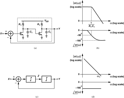
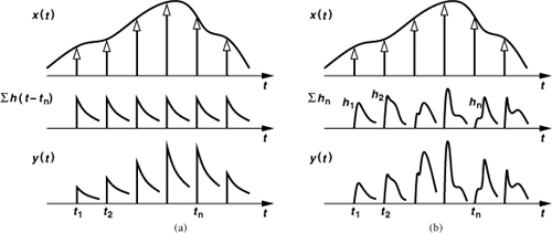
Our study thus far allows us to predict the frequency of oscillation: we seek the frequency at which the total phase shift around the loop is 360° and determine whether the loop gain reaches unity at this frequency. (An exception is described in the example below.) This calculation, however, does not predict the oscillation amplitude. In a perfectly linear loop, the oscillation amplitude is simply given by the initial conditions residing on the storage elements if the loop gain is equal to unity at the oscillation frequency. The following example illustrates this point.


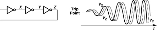
Other oscillators behave differently from the two-integrator loop: they may begin to oscillate at a frequency at which the loop gain is higher than unity, thereby experiencing an exponential growth in their output amplitude. In an actual circuit, the growth eventually stops due to the saturating behavior of the amplifier(s) in the loop. For example, consider the cascade of three CMOS inverters depicted in Fig. 8.11 (called a “ring oscillator”). If the circuit is released with X, Y, and Z at the trip point of the inverters, then each stage operates as an amplifier, leading to an oscillation frequency at which each inverter contributes a frequency-dependent phase shift of 60°. (The three inversions make this a negative-feedback loop at low frequencies.) With the high loop gain, the oscillation amplitude grows exponentially until the transistors enter the triode region at the peaks, thus lowering the gain. In the steady state, the output of each inverter swings from nearly zero to nearly VDD.
Figure 8.11 Ring oscillator and its waveforms.
In most oscillator topologies of interest to us, the voltage swings are defined by the saturating behavior of differential pairs. The following example elaborates on this point.
The inductively-loaded differential pair shown in Fig. 8.12(a) is driven by a large input sinusoid at ![]() . Plot the output waveforms and determine the output swing.
. Plot the output waveforms and determine the output swing.
Figure 8.12 (a) Differential pair with tank loads, (b) drain currents, (c) first harmonic of a square wave.
Solution:
![]()
8.2.2 One-Port View of Oscillators
In the previous section, we considered oscillators as negative-feedback systems that experience sufficient positive feedback at some frequency. An alternative perspective views oscillators as two one-port components, namely, a lossy resonator and an active circuit that cancels the loss. This perspective provides additional insight and is described in this section.
Suppose, as shown in Fig. 8.13(a), a current impulse, I0δ(t), is applied to a lossless tank. The impulse is entirely absorbed by C1 (why?), generating a voltage of I0/C1. The charge on C1 then begins to flow through L1, and the output voltage falls. When Vout reaches zero, C1 carries no energy but L1 has a current equal to L1dVout/dt, which charges C1 in the opposite direction, driving Vout toward its negative peak. This periodic exchange of energy between C1 and L1 continues indefinitely, with an amplitude given by the strength of the initial impulse.
Figure 8.13 (a) Response of an ideal tank to an impulse, (b) response of a lossy tank to an impulse, (c) cancellation of loss by negative resistance.
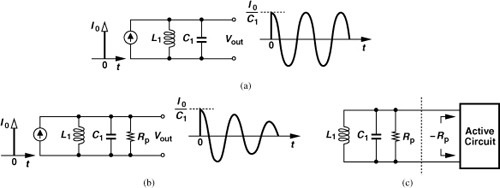
Now, let us assume a lossy tank. Depicted in Fig. 8.13(b), such a circuit behaves similarly except that Rp drains and “burns” some of the capacitor energy in every cycle, causing an exponential decay in the amplitude. We therefore surmise that, if an active circuit replenishes the energy lost in each period, then the oscillation can be sustained. In fact, we predict that an active circuit exhibiting an input resistance of −Rp can be attached across the tank to cancel the effect of Rp, thereby recreating the ideal scenario shown in Fig. 8.13(a). Illustrated in Fig. 8.13(c), the resulting topology is called a “one-port oscillator.”
How can a circuit present a negative (small-signal) input resistance? Figure 8.14(a) shows an example, where two capacitors are tied from the gate and drain of a transistor to its source. The impedance Zin can be obtained by noting that C1 carries a current equal to −IX, generating a gate-source voltage of −IX/(C1s) and hence a drain current of −IXgm/(C1s). The difference between IX and the drain current flows through C2, producing a voltage equal to [IX + IXgm/(C1s)]/(C2s). This voltage must be equal to VGS + VX:
![]()
Figure 8.14 (a) Circuit providing negative resistance, (b) equivalent circuit.
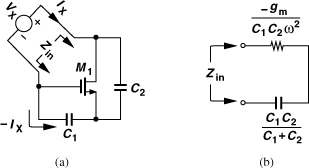
It follows that
![]()
For a sinusoidal input, s = jω,
![]()
Thus, the input impedance can be viewed as a series combination of C1, C2, and a negative resistance equal to −gm/(C1C2ω2) [Fig. 8.14(b)]. Interestingly, the negative resistance varies with frequency.
Having found a negative resistance, we can now attach it to a lossy tank so as to construct an oscillator. Since the capacitive component in Eq. (8.24) can become part of the tank, we simply connect an inductor to the negative-resistance port (Fig. 8.15), seeking the condition for oscillation. In this case, it is simpler to model the loss of the inductor by a series resistance, RS. The circuit oscillates if
![]()
Figure 8.15 Connection of lossy inductor to negative-resistance circuit.
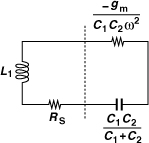
Under this condition, the circuit reduces to L1 and the series combination of C1 and C2, exhibiting an oscillation frequency of

As expected, for oscillation to occur, the transistor in Fig. 8.14(a) must provide sufficient “strength” (transconductance). In fact, (8.30) implies that the minimum allowable gm is obtained if C1 = C2. That is, gmRp ≥ 4.
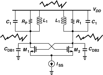
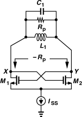
8.3 Cross-Coupled Oscillator
In this section, we develop an LC oscillator topology that, owing to its robust operation, has become the dominant choice in RF applications. We begin the development with a feedback system, but will discover that the result also lends itself to the one-port view described in Section 8.2.2.
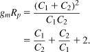
We wish to build a negative-feedback oscillatory system using “LC-tuned” amplifier stages. Figure 8.16(a) shows such a stage, where C1 denotes the total capacitance seen at the output node and Rp the equivalent parallel resistance of the tank at the resonance frequency. We neglect CGD here but will see that it can be readily included in the final oscillator topology.
Figure 8.16 (a) Tuned amplifier, (b) frequency response.
Let us examine the frequency response of the stage. At very low frequencies, L1 dominates the load and
![]()
That is, |Vout/Vin| is very small and ∠(Vout/Vin) remains around −90° [Fig. 8.16(b)]. At the resonance frequency, ω0, the tank reduces to Rp and
![]()
The phase shift from the input to the output is thus equal to −180°. At very high frequencies, C1 dominates, yielding
![]()
Thus, |Vout/Vin| diminishes and ∠(Vout/Vin) approaches + 90° (= −270°).
Can the circuit of Fig. 8.16(a) oscillate if its input and output are shorted? As evidenced by the open-loop magnitude and phase plots shown in Fig. 8.16(b), no frequency satisfies Barkhausen’s criteria; the total phase shift fails to reach 360° at any frequency.
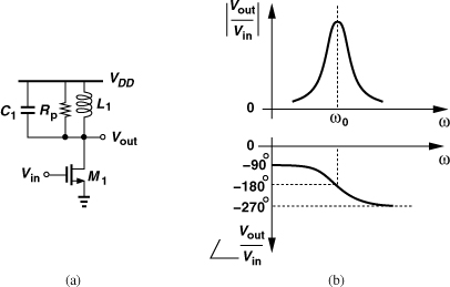
Upon closer examination, we recognize that the circuit provides a phase shift of 180° with possibly adequate gain (gmRp) at ω0. We simply need to increase the phase shift to 360°, perhaps by inserting another stage in the loop. Illustrated in Fig. 8.17(a), the idea is to cascade two identical LC-tuned stages so that, at resonance, the total phase shift around the loop is equal to 360°. The circuit oscillates if the loop gain is equal to or greater than unity:
![]()
Figure 8.17 Cascade of two tuned amplifiers in feedback loop.
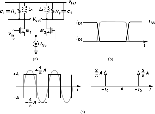
The above circuit can be redrawn as shown in Fig. 8.18(a) and is called a “cross-coupled” oscillator due to the connection of M1 and M2. Forming the core of most RF oscillators used in practice, this topology entails many interesting properties and will be studied from different perspectives in this chapter.
Figure 8.18 (a) Simple cross-coupled oscillator, (b) addition of tail current, (c) equivalence to a differential pair placed in feedback.

Let us compute the oscillation frequency of the circuit. The capacitance at X includes CGS2, CDB1, and the effect of CGD1 and CGD2. We note that (a) CGD1 and CGD2 are in parallel, and (b) the total voltage change across CGD1 + CGD2 is equal to twice the voltage change at X (or Y) because VX and VY vary differentially. Thus,
![]()
Here, C1 denotes the parasitic capacitance of L1 plus the input capacitance of the next stage.
The oscillator of Fig. 8.18(a) suffers from poorly-defined bias currents. Since the average VGS of each transistor is equal to VDD, the currents strongly depend on the mobility, threshold voltage, and temperature. With differential VX and VY, we surmise that M1 and M2 can operate as a differential pair if they are tied to a tail current source. Shown in Fig. 8.18(b), the resulting circuit is more robust and can be viewed as an inductively-loaded differential pair with positive feedback [Fig. 8.18(c)]. The oscillation amplitude grows until the pair experiences saturation. We sometimes refer to this circuit as the “tail-biased oscillator” to distinguish it from other cross-coupled topologies.
The above-supply swings in the cross-coupled oscillator of Fig. 8.18(b) raise concern with respect to transistor reliability. The instantaneous voltage difference between any two terminals of M1 or M2 must remain below the maximum value allowed by the technology. Figure 8.19 shows a “snapshot” of the circuit when M1 is off and M2 is on. Each transistor may experience stress under the following conditions: (1) The drain reaches VDD + Va, where Va is the peak single-ended swing, e.g., (2/π)ISSRp, while the gate drops to VDD − Va. The transistor remains off, but its drain-gate voltage is equal to 2Va and its drain-source voltage is greater than 2Va (why?). (2) The drain falls to VDD − Va while the gate rises to VDD + Va. Thus, the gate-drain voltage reaches 2Va and the gate-source voltage exceeds 2Va. We note that both VDS1 and VGS2 may assume excessively large values. Proper choice of Va, ISS, and device dimensions avoids stressing the transistors.
Figure 8.19 Voltage swings in cross-coupled oscillator.2

The reader may wonder how the inductance value and the device dimensions are selected in the cross-coupled oscillator. We defer the design procedure to after we have studied voltage-controlled oscillators and phase noise (Section 8.8).
While conceived as a feedback system, the cross-coupled oscillator also lends itself to the one-port view described in Section 8.2.2. Let us first redraw the circuit as shown in Fig. 8.21(a) and note that, for small differential waveforms at X and Y, VN does not change even if it is not connected to VDD. Disconnecting this node from VDD (only for small-signal analysis) and recognizing that the series combination of two identical tanks can be represented as a single tank, we arrive at the circuit depicted in Fig. 8.21(b). We can now view the oscillator as a lossy resonator (2L1, C1/2, and 2Rp) tied to the port of an active circuit (M1, M2, and ISS), expecting that the latter replenishes the energy lost in the former. That is, Z1 must contain a negative resistance. This can be seen from the equivalent circuit shown in Fig. 8.21(c), where V1 − V2 = VX and
![]()
Figure 8.21 (a) Redrawing of cross-coupled oscillator, (b) load tanks merged, (c) equivalent circuit of cross-coupled pair.

It follows that
![]()
which, for gm1 = gm2 = gm, reduces to
![]()
For oscillation to occur, the negative resistance must cancel the loss of the tank:
![]()
and hence
![]()
As expected, this condition is identical to that expressed by Eq. (8.34).3
Choice of gm
The foregoing studies may suggest that the gm of the cross-coupled transistors in Fig. 8.18(b) can be chosen slightly greater than Rp of the tank to ensure oscillation. However, this choice leads to small voltage swings; if the swings are large, e.g., if M1 and M2 switch completely, then the gm falls below 1/Rp for part of the period, failing to sustain oscillation. (That is, with gm ≈ 1/Rp, M1 and M2 must remain linear to avoid compression.) In practice, therefore, we design the circuit for nearly complete current steering between M1 and M2, inevitably choosing a gm quite higher than 1/Rp.
8.4 Three-Point Oscillators
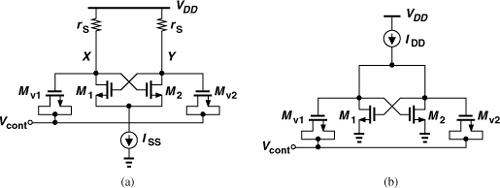
As observed in Section 8.2.2, the circuit of Fig. 8.14(a) can be attached to an inductor so as to form an oscillator. Note that the derivation of the impedance Zin does not assume any terminal is grounded. Thus, three different oscillator topologies can be obtained by grounding each of the transistor terminals. Figures 8.22(a), (b), and (c) depict the resulting circuits if the source, the gate, or the drain is (ac) grounded, respectively. In each case, a current source defines the bias current of the transistor. [The gate of M1 in Fig. 8.22(b) and the left terminal of L1 in Fig. 8.22(c) must be tied to a proper potential, e.g., Vb − VDD.]
Figure 8.22 Variants of three-point oscillator, (a) with source grounded, (b) with gate grounded (Colpitts oscillator), (c) with drain grounded (Clapp oscillator).
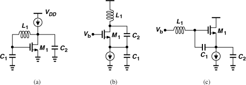
It is important to bear in mind that the operation frequency and startup condition of all three oscillators in Fig. 8.22 are given by Eqs. (8.26) and (8.30), respectively. Specifically, the transistor must provide sufficient transconductance to satisfy
![]()
if C1 = C2. This condition is more stringent than Eq. (8.34) for the cross-coupled oscillator, suggesting that the circuits of Fig. 8.22 may fail to oscillate if the inductor Q is not very high. This is the principal disadvantage of these oscillators and the reason for their lack of popularity.
Another drawback of the circuits shown in Fig. 8.22 is that they produce only single-ended outputs. It is possible to couple two copies of one oscillator so that they operate differentially. Shown in Fig. 8.23 is an example, where two instances of the oscillator in Fig. 8.22(c) are coupled at node P. Resistor R1 establishes a dc level equal to VDD at P and at the gates of M1 and M2. More importantly, if chosen properly, this resistor prohibits common-mode oscillation. To understand this point, suppose X and Y swing in phase and so do A and B, creating in-phase currents through L1 and L2. The two half circuits then collapse into one, and R1 appears in series with the parallel combination of L1 and L2, thereby lowering their Q. No CM oscillation can occur if R1 is sufficiently large. For differential waveforms, on the other hand, L1 and L2 carry equal and opposite currents, forcing P to ac ground.
Figure 8.23 Differential version of a three-point oscillator.
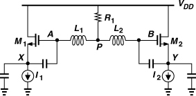
Even with differential outputs, the circuit of Fig. 8.23 may be inferior to the cross-coupled oscillator of Fig. 8.18(b)—not only for the more stringent startup condition but also because the noise of I1 and I2 directly corrupts the oscillation. The circuit nonetheless has been used in some designs.
8.5 Voltage-Controlled Oscillators
Most oscillators must be tuned over a certain frequency range. We therefore wish to construct oscillators whose frequency can be varied electronically. “Voltage-controlled oscillators” (VCOs) are an example of such circuits.
Figure 8.24 conceptually shows the desired behavior of a VCO. The output frequency varies from ω1 to ω2 (the required tuning range) as the control voltage, Vcont, goes from V1 to V2. The slope of the characteristic, KVCO, is called the “gain” or “sensitivity” of the VCO and expressed in rad/Hz/V. We formulate this characteristic as
![]()
where ω0 denotes the intercept point on the vertical axis. As explained in Chapter 9, it is desirable that this characteristic be relatively linear, i.e., KVCO not change significantly across the tuning range.
Figure 8.24 VCO characteristic.

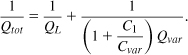
In order to vary the frequency of an LC oscillator, the resonance frequency of its tank(s) must be varied. Since it is difficult to vary the inductance electronically, we only vary the capacitance by means of a varactor. As explained in Chapter 7, MOS varactors are more commonly used than pn junctions, especially in low-voltage design. We thus construct our first VCO as shown in Fig. 8.25(a), where varactors MV1 and MV2 appear in parallel with the tanks (if Vcont is provided by an ideal voltage source). Note that the gates of the varactors are tied to the oscillator nodes and the source/drain/n-well terminals to Vcont. This avoids loading X and Y with the capacitance between the n-well and the substrate.
Figure 8.25 (a) VCO using MOS varactors, (b) range of varactor capacitance used in (a).
Since the gates of MV1 and MV2 reside at an average level equal to VDD, their gate-source voltage remains positive and their capacitance decreases as Vcont goes from zero to VDD [Fig. 8.25(b)]. This behavior persists even in the presence of large voltage swings at X and Y and hence across MV1 and MV2. The key point here is that the average voltage across each varactor varies from VDD to zero as Vcont goes from zero to VDD, thus creating a monotonic decrease in their capacitance. The oscillation frequency can thus be expressed as
![]()
where Cvar denotes the average value of each varactor’s capacitance.
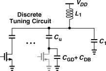
The reader may wonder why capacitors C1 have been included in the oscillator of Fig. 8.25(a). It appears that, without C1, the varactors can vary the frequency to a greater extent, thereby providing a wider tuning range. This is indeed true, and we rarely need to add a constant capacitance to the tank deliberately. In other words, C1 simply models the inevitable capacitances appearing at X and Y: (1) CGS, CGD (with a Miller multiplication factor of two), and CDB of M1 and M2, (2) the parasitic capacitance of each inductor, and (3) the input capacitance of the next stage (e.g., a buffer, divider, or mixer). As mentioned in Chapter 4, the last component becomes particularly significant on the transmit side due to the “propagation” of the capacitance from the input of the PA to the input of the upconversion mixers.
The above VCO topology merits two remarks. First, the varactors are stressed for part of the period if Vcont is near ground and VX (or VY) rises significantly above VDD. Second, as depicted in Fig. 8.25(b), only about half of Cmax − Cmin is utilized in the tuning. We address these issues later in this chapter.
As explained in Chapter 7, symmetric spiral inductors excited by differential waveforms exhibit a higher Q than their single-ended counterparts. For this reason, L1 and L2 in Fig. 8.25 are typically realized as a single symmetric structure. Figure 8.26 illustrates the idea and its circuit representation. The point of symmetry of the inductor (its “center tap”) is tied to VDD. In some of our analyses, we omit the center tap connection for the sake of simplicity.
Figure 8.26 Oscillator using symmetric inductor.
The VCO of Fig. 8.25(a) provides an output CM level near VDD, an advantage or disadvantage depending on the next stage (Section 8.9).
8.5.1 Tuning Range Limitations
While a robust, versatile topology, the cross-coupled VCO of Fig. 8.25(a) suffers from a narrow tuning range. As mentioned above, the three components comprising C1 tend to limit the effect of the varactor capacitance variation. Since in (8.50), Cvar tends to be a small fraction of the total capacitance, we make a crude approximation, Cvar ![]() C1, and rewrite (8.50) as
C1, and rewrite (8.50) as
![]()
If the varactor capacitance varies from Cvar1 to Cvar2, then the tuning range is given by
![]()
For example, if Cvar2 − Cvar1 = 20%C1, then the tuning range is about ±5% around the center frequency.
What limits the capacitance range of the varactor, Cvar2 − Cvar1? We note from Chapter 7 that Cvar2 − Cvar1 trades with the Q of the varactor: a longer channel reduces the relative contribution of the gate-drain and gate-source overlap capacitances, widening the range but lowering the Q. Thus, the tuning range trades with the overall tank Q (and hence with the phase noise).
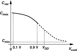
Another limitation on Cvar2 − Cvar1 arises from the available range for the control voltage of the oscillator, Vcont in Fig. 8.25(a). This voltage is generated by a “charge pump” (Chapter 9), which, as any other analog circuit, suffers from a limited output voltage range. For example, a charge pump running from a 1-V supply may not be able to generate an output below 0.1 V or above 0.9 V. The characteristic of Fig. 8.25(b) therefore reduces to that depicted in Fig. 8.27.
Figure 8.27 Varactor range used with input limited between 0.1 V and 0.9 V.
The foregoing tuning limitations prove serious in LC VCO design. We introduce in Section 8.6 a number of oscillator topologies that provide a wider tuning range—but at the cost of other aspects of the performance.
8.5.2 Effect of Varactor Q
As observed in the previous section, the varactor capacitance is but a small fraction of the total tank capacitance. We therefore surmise that the resistive loss of the varactor lowers the overall Q of the tank only to some extent. Let us begin with a fundamental observation.
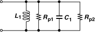
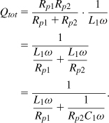
To quantify the effect of varactor loss, consider the tank shown in Fig. 8.29(a), where Rp1 models the loss of the inductor and Rvar the equivalent series resistance of the varactor. We wish to compute the Q of the tank. Transforming the series combination of Cvar and Rvar to a parallel combination [Fig. 8.29(b)], we have from Chapter 2
![]()
Figure 8.29 (a) Tank using lossy varactor, (b) equivalent circuit.

To utilize our previous results, we combine C1 and Cvar. The Q associated with C1 + Cvar is equal to
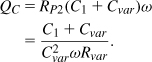
Recognizing that Qvar = (CvarωRvar)−1, we have
![]()
In other words, the Q of the varactor is “boosted” by a factor of 1 + C1/Cvar. The overall tank Q is therefore given by
For frequencies as high as several tens of gigahertz, the first term in Eq. (8.64) is dominant (unless a long channel is chosen for the varactors).
Equation (8.64) can be generalized if the tank consists of an ideal capacitor, C1, and lossy capacitors, C2-Cn, that exhibit a series resistance of R2-Rn, respectively. The reader can prove that
![]()
where Ctot = C1 + ... + Cn and Qj = (RjCjω)−1.
8.6 LC VCOs with Wide Tuning Range
8.6.1 VCOs with Continuous Tuning
The tuning range obtained from the C–V characteristic depicted in Fig. 8.27 may prove prohibitively narrow, particularly because the capacitance range corresponding to negative VGS (for Vcont > VDD) remains unused. We must therefore seek oscillator topologies that allow both positive and negative (average) voltages across the varactors, utilizing almost the entire range from Cmin to Cmax.
Figure 8.30(a) shows one such topology. Unlike the tail-biased configuration studied in Section 8.3, this circuit defines the bias currents of M1 and M2 by a top current source, IDD. We analyze this circuit by first computing the output common-mode level. In the absence of oscillation, the circuit reduces to that shown in Fig. 8.30(b), where M1 and M2 share IDD equally and are configured as diode-connected devices. Thus, the CM level is simply given by the gate-source voltage of a diode-connected transistor carrying a current of IDD/2.4 For example, for square-law devices,
![]()
Figure 8.30 (a) Top-biased VCO, (b) equivalent circuit for CM calculation, (c) varactor range used.
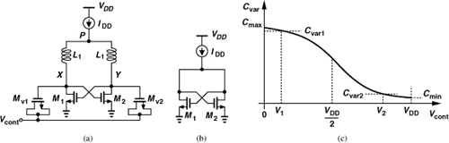
We select the transistor dimensions such that the CM level is approximately equal to VDD/2. Consequently, as Vcont varies from 0 to VDD, the gate-source voltage of the varactors, VGS,var, goes from + VDD/2 to −VDD/2, sweeping almost the entire capacitance range from Cmin to Cmax [Fig. 8.30(c)]. In practice, the circuit producing Vcont (the charge pump) can handle only the voltage range from V1 to V2, yielding a capacitance range from Cvar1 to Cvar2.
The startup condition, oscillation frequency, and output swing of the oscillator shown in Fig. 8.30(a) are similar to those derived for the tail-biased circuit of Fig. 8.18(b). Also, L1 and L2 are realized as a single symmetric inductor so as to achieve a higher Q; the center tap of the inductor is tied to IDD.
While providing a wider range than its tail-biased counterpart, the topology of Fig. 8.30(a) suffers from a higher phase noise. As studied in Section 8.7, this penalty arises primarily from the modulation of the output CM level (and hence the varactors) by the noise current of IDD, as evidenced by Eq. (8.66). This effect does not occur in the tail-biased oscillator because the output CM level is “pinned” at VDD by the low dc resistance of the inductors. The following example illustrates this difference.
Solution:
Figure 8.31 Output CM dependence on bias current in (a) tail-biased and (b) top-biased VCOs.

In order to avoid varactor modulation due to the noise of the bias current source, we return to the tail-biased topology but employ ac coupling between the varactors and the core so as to allow positive and negative voltages across the varactors. Illustrated in Fig. 8.32(a), the idea is to define the dc voltage at the gate of the varactors by Vb (≈ VDD/2) rather than VDD. Thus, in a manner similar to that shown in Fig. 8.30(c), the voltage across each varactor goes from −VDD/2 to + VDD/2 as Vcont varies from 0 to VDD, maximizing the tuning range.
Figure 8.32 (a) VCO using capacitor coupling to varactors, (b) reduction of tuning range as a result of finite CS1 and CS2.
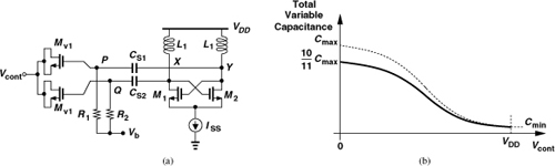
The principal drawback of the above circuit stems from the parasitics of the coupling capacitors. In Fig. 8.32(a), CS1 and CS2 must be much greater than the maximum capacitance of the varactors, Cmax, so that the capacitance range presented by the varactors to the tanks does not shrink substantially. If CS1 = CS2 = CS, then in Eq. (8.53), Cvar2 and Cvar1 must be placed in series with CS, yielding
![]()
For example, if CS = 10Cmax, then the series combination yields a maximum capacitance of (10Cmax · Cmax)/(11Cmax) = (10/11)Cmax, i.e., about 10% less than Cmax. Thus, as shown in Fig. 8.32(b), the capacitance range decreases by about 10%. Equivalently, the maximum-to-minimum capacitance ratio falls from Cmax/Cmin to (10Cmax + Cmin)/(11Cmin) ≈ (10/11)(Cmax/Cmin).
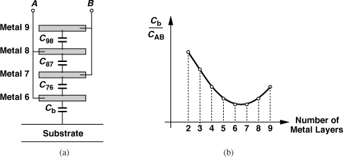
The choice of CS = 10Cmax reduces the capacitance range by 10% but introduces substantial parasitic capacitances at X and Y or at P and Q. This is because integrated capacitors suffer from parasitic capacitances to the substrate. An example is depicted in Fig. 8.33(a), where a sandwich of metal layers from metal 6 to metal 9 forms the wanted capacitance between nodes A and B, and the capacitance between the bottom layer and the substrate, Cb, appears from node A to ground. We must therefore choose the number of layers in the sandwich so as to minimize Cb/CAB. Plotted in Fig. 8.33(b) is this ratio as a function of the number of the layers, assuming that we begin with the top layers. For only metal 9 and metal 8, Cb is small, but so is CAB. As more layers are stacked, Cb increases more slowly than CAB does, yielding a declining ratio. As the bottom layer approaches the substrate, Cb begins to increase more rapidly than CAB, producing the minimum shown in Fig. 8.33(b). In other words, Cb/CAB typically exceeds 5%.
Figure 8.33 (a) Capacitor realized as parallel metal plates, (b) relative parasitic capacitance as a function of the number of metal layers.
Let us now study the effect of the parasitics of CS1 and CS2 in Fig. 8.32(a). From Eq. (8.53), we note that a larger C1 further limits the tuning range. In other words, the numerator of (8.53) decreases due to the series effect of CS, and the denominator of (8.53) increases due to the parasitic capacitance of CS. To formulate these limitations, we assume a typical case, Cmax ≈ 2Cmin, and also Cvar2 ≈ Cmax, Cvar1 ≈ Cmin, CS = 10Cmax, and Cb = 0.05CS = 0.5Cmax. Equation (8.69) thus reduces to
In the above study, we have assumed that Cb appears at nodes X and Y in Fig. 8.32(a). Alternatively, Cb can be placed at nodes P and Q. We study this case in Problem 8.8, arriving at similar limitations in the tuning range.
A capacitor structure that exhibits lower parasitics than the metal sandwich geometry of Fig. 8.33(a) is shown in Fig. 8.34(a). Called a “fringe” or “lateral-field” capacitor, this topology incorporates closely-spaced narrow metal lines to maximize the fringe capacitance between them. The capacitance per unit volume is larger than that of the metal sandwich, leading to a smaller parasitic.
Figure 8.34 (a) Fringe capacitor, (b) distributed view of parallel-plate capacitor.

Three other issues in Fig. 8.32(a) merit consideration. First, since R1 and R2 appear approximately in parallel with the tanks, their value must be chosen much greater than Rp. (Even a tenfold ratio proves inadequate as it lowers the Q by about 10%.) Second, noise on the mid-supply bias, Vb, directly modulates the varactors and must therefore be minimized. Third, as studied in the transceiver design example of Chapter 13, the noise of R1 and R2 modulates the varactors, producing substantial phase noise.
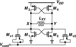
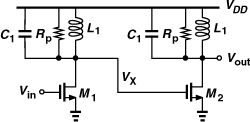
Another VCO topology that naturally provides an output CM level approximately equal to VDD/2 is shown in Fig. 8.35. The circuit can be viewed as two back-to-back CMOS inverters, except that the sources of the NMOS devices are tied to a tail current, or as a cross-coupled NMOS pair and a cross-coupled PMOS pair sharing the same bias current. Proper choice of device dimensions and ISS can yield a CM level at X and Y around VDD/2, thereby maximizing the tuning range.
Figure 8.35 VCO using NMOS and PMOS cross-coupled pairs.
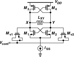
In this circuit, the bias current is “reused” by the PMOS devices, providing a higher transconductance. But a more important advantage of the above topology over those in Figs. 8.25(a), 8.30(a), and 8.32(a) is that it produces twice the voltage swing for a given bias current and inductor design. To understand this point, we assume LXY in the complementary topology is equal to L1 + L2 in the previous circuits. Thus, LXY presents an equivalent parallel resistance of 2Rp. Drawing the circuit for each half cycle as shown in Fig. 8.36, we recognize that the current in each tank swings between +ISS and −ISS, whereas in previous topologies it swings between ISS and zero. The output voltage swing is therefore doubled.
Figure 8.36 Current flow through floating resonator when (a) M1 and M4 are on, and (b) M2 and M3 are on.
The circuit of Fig. 8.35 nonetheless suffers from two drawbacks. First, for |VGS3| + VGS1 + VISS to be equal to VDD, the PMOS transistors must typically be quite wide, contributing significant capacitance and limiting the tuning range. This is particularly troublesome at very high frequencies, requiring a small inductor and diminishing the above swing advantage. Second, as in the circuit of Fig. 8.30(a), the noise current of the bias current source modulates the output CM level and hence the capacitance of the varactors, producing frequency and phase noise. Following Example 8.17, the reader can show that a change of ΔI in ISS results in a change of (ΔI/2)/gm3,4 in the voltage across each varactor and hence a frequency change of KVCO(ΔI/2)/gm3,4. Owing to the small headroom available for ISS, the noise current of ISS, given by 4kTγ gm, tends to be large.
8.6.2 Amplitude Variation with Frequency Tuning
In addition to the narrow varactor capacitance range, another factor that limits the useful tuning range is the variation of the oscillation amplitude. As the capacitance attached to the tank increases, the amplitude tends to decrease. To formulate this effect, suppose the tank inductor exhibits only a series resistance, RS, (due to metal resistance and skin effect). Recall from Chapter 2 that, for a narrow frequency range and a Q greater than 3,
![]()
and hence
![]()
Thus, Rp falls in proportion to ω2 as more capacitance is presented to the tank.5 For example, a 10% change in ω yields a 20% change in the amplitude.
8.6.3 Discrete Tuning
Our study of varactor tuning in Example 8.18 points to a relatively narrow range. The use of large varactors leads to a high KVCO, making the circuit sensitive to noise on the control voltage. In applications where a substantially wider tuning range is necessary, “discrete tuning” may be added to the VCO so as to achieve a capacitance range well beyond Cmax/Cmin of varactors. Illustrated in Fig. 8.38(a) and similar to the discrete tuning technique described in Chapter 5 for LNAs, the idea is to place a bank of small capacitors, each having a value of Cu, in parallel with the tanks and switch them in or out to adjust the resonance frequency. We can also view Vcont as a “fine control” and the digital input to the capacitor bank as a “coarse control.” Figure 8.38(b) shows the tuning behavior of the VCO as a function of both controls. The fine control provides a continuous but narrow range, whereas the coarse control shifts the continuous characteristic up or down.
Figure 8.38 (a) Discrete tuning by means of switched capacitors, (b) resulting characteristics.
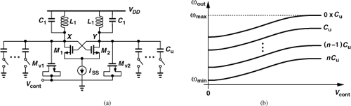
The overall tuning range can be calculated as follows. With ideal switches and unit capacitors, the lowest frequency is obtained if all of the capacitors are switched in and the varactor is at its maximum value, Cmax:
![]()
The highest frequency occurs if the unit capacitors are switched out and the varactor is at its minimum value, Cmin:
![]()
Of course, as expressed by Eq. (8.77), the oscillation amplitude may vary considerably across this range, requiring “overdesign” at ωmax (or calibration) so as to obtain reasonable swings at ωmin.
The discrete tuning technique shown in Fig. 8.38(a) entails several difficult issues. First, the on-resistance, Ron, of the switches that control the unit capacitors degrades the Q of the tank. Applying Eq. (8.65) to the parallel combination shown in Fig. 8.40 and denoting [(Ron/n)(nCu)ω]−1 by Qbank, we have
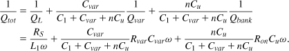
Figure 8.40 Equivalent circuit for Q calculation.

Can we simply increase the width of the switch transistors in Fig. 8.38(a) so as to minimize the effect of Ron? Unfortunately, wider switches introduce a larger capacitance from the bottom plate of the unit capacitors to ground, thereby presenting a substantial capacitance to the tanks when the switches are off. As shown in Fig. 8.41, each branch in the bank contributes a capacitance of CGD + CDB to the tank if Cu ![]() CGD + CDB. For n branches, therefore, C1 incurs an additional constant component equal to n(CGD + CDB), further limiting the fine tuning range. For example, Δωosc1 in Eq. (8.80) must be rewritten as
CGD + CDB. For n branches, therefore, C1 incurs an additional constant component equal to n(CGD + CDB), further limiting the fine tuning range. For example, Δωosc1 in Eq. (8.80) must be rewritten as
![]()
Figure 8.41 Effect of switch parasitic capacitances.
This trade-off between the Q and the tuning range limits the use of discrete tuning.
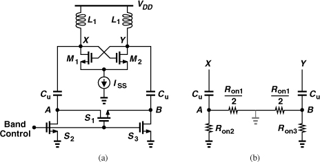
The problem of switch on-resistance can be alleviated by exploiting the differential operation of the oscillator. Illustrated in Fig. 8.42(a), the idea is to place the main switch, S1, between nodes A and B so that, with differential swings at these nodes, only half of Ron1 appears in series with each unit capacitor [Fig. 8.42(b)]. This allows a twofold reduction in the switch width for a given resistance. Switches S2 and S3 are minimum-size devices, merely defining the CM level of A and B.
Figure 8.42 (a) Use of floating switch, (b) equivalent circuit.
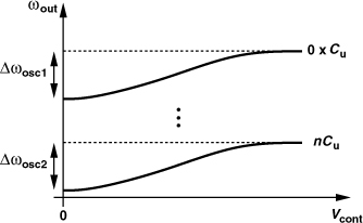
The second issue in discrete tuning relates to potential “blind” zones. Suppose, as shown in Fig. 8.43(a), unit capacitor number j is switched out, creating a frequency change equal to ω4 − ω2 ≈ ω3 − ω1, but the fine tuning range provided by the varactor, ω4 − ω3, is less than ω4 − ω2. Then, the oscillator fails to cover the range between ω2 and ω3 for any combination of fine and coarse controls.
Figure 8.43 (a) Blind zone in discrete tuning, (b) overlap between consecutive characteristics to avoid blind zone.
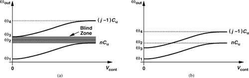
To avoid blind zones, each two consecutive tuning characteristics must have some overlap. Depicted in Fig. 8.43(b), this precaution translates to smaller unit capacitors but a larger number of them and hence a complex layout. As explained in Chapter 13, the unit capacitors can be chosen unequal to mitigate this issue. Note that the overlap is also necessary to avoid excessive variation of KVCO near the ends of each tuning curve. For example, around ω2 in Fig. 8.43(b), the lower tuning curve flattens out, requiring that the upper one be used.
Some recent designs have employed oscillators with only discrete tuning. Called “digitally-controlled oscillators” (DCOs), such circuits must employ very fine frequency stops. Examples are described in [2].
In Chapter 13, we design and simulate a VCO with continuous and discrete tuning for 11a/g applications.
8.7 Phase Noise
The design of VCOs must deal with trade-offs among tuning range, phase noise, and power dissipation. Our study has thus far focused on the task of tuning. We now turn our attention to phase noise.
8.7.1 Basic Concepts
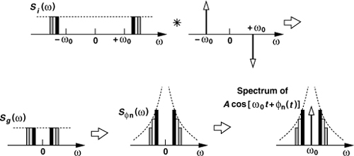
An ideal oscillator produces a perfectly-periodic output of the form x(t) = A cos ωct. The zero crossings occur at exact integer multiples of Tc = 2π/ωc. In reality, however, the noise of the oscillator devices randomly perturbs the zero crossings. To model this perturbation, we write x(t) = A cos[ωct + φn(t)], where φn(t) is a small random phase quantity that deviates the zero crossings from integer multiples of Tc. Figure 8.44 illustrates the two waveforms in the time domain. The term φn(t) is called the “phase noise.”
Figure 8.44 Output waveforms of an ideal and a noisy oscillator.
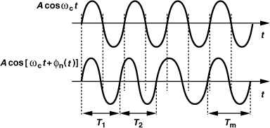
The waveforms in Fig. 8.44 can also be viewed from another, slightly different, perspective. We can say that the period remains constant if x(t) = A cos ωct but varies randomly if x(t) = A cos[ωct + φn(t)] (as indicated by T1, ..., Tm in Fig. 8.44). In other words, the frequency of the waveform is constant in the former case but varies randomly in the latter. This observation leads to the spectrum of the oscillator output. For x(t) = A cos ωct, the spectrum consists of a single impulse at ωc [Fig. 8.45(a)], whereas for x(t) = A cos[ωct + φn(t)] the frequency experiences random variations, i.e., it departs from ωc occasionally. As a consequence, the impulse is “broadened” to represent this random departure [Fig. 8.45(b)].
Figure 8.45 Output spectra of (a) an ideal, and (b) a noisy oscillator.


Our focus on noise in the zero crossings rather than noise on the amplitude arises from the assumption that the latter is removed by hard switching in stages following the oscillator. For example, the switching transistors in an active mixer spend little time near equilibrium, “masking” most of the LO amplitude noise for the rest of the time.
The spectrum of Fig. 8.45(b) can be related to the time-domain expression. Since φn(t) ![]() 1 rad,
1 rad,
That is, the spectrum of x(t) consists of an impulse at ωc and the spectrum of φn(t) translated to a center frequency of ωc. Thus, the declining skirts in Fig. 8.45(b) in fact represent the behavior of φn(t) in the frequency domain.
In phase noise calculations, many factors of 2 or 4 appear at different stages and must be carefully taken into account. For example, as illustrated in Fig. 8.47, (1) since φn(t) in Eq. (8.88) is multiplied by sin ωct, its power spectral density, Sφn, is multiplied by 1/4 as it is translated to ±ωc; (2) A spectrum analyzer measuring the resulting spectrum folds the negative-frequency spectrum atop the positive-frequency spectrum, raising the spectral density by a factor of 2.
Figure 8.47 Various factors of 4 and 2 that arise in conversion of noise to phase noise.

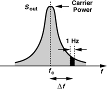
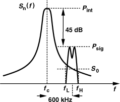
How is the phase noise quantified? Since the phase noise falls at frequencies farther from ωc, it must be specified at a certain “frequency offset,” i.e., a certain difference with respect to ωc. As shown in Fig. 8.48, we consider a 1-Hz bandwidth of the spectrum at an offset of Δf, measure the power in this bandwidth, and normalize the result to the “carrier power.” The carrier power can be viewed as the peak of the spectrum or (more rigorously) as the power given by Eq. (8.86), namely, A2/2. For example, the phase noise of an oscillator in GSM applications must fall below −115 dBc/Hz at 600-kHz offset. Called “dB with respect to the carrier,” the unit dBc signifies normalization of the noise power to the carrier power.
Figure 8.48 Specification of phase noise.
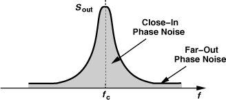
In practice, the phase noise reaches a constant floor at large frequency offsets (beyond a few megahertz) (Fig. 8.49). We call the regions near and far from the carrier the “close-in” and the “far-out” phase noise, respectively, although the border between the two is vague.
Figure 8.49 Close-in and far-out phase noise.
8.7.2 Effect of Phase Noise
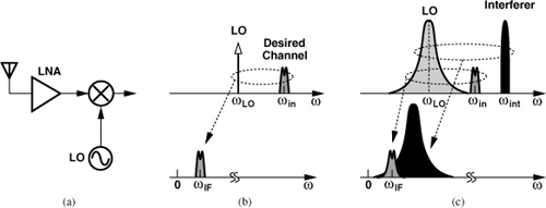
To understand the effect of phase noise in RF systems, let us consider the receiver front end shown in Fig. 8.50(a) and study the downconverted spectrum. Referring to the ideal case depicted in Fig. 8.50(b), we observe that the desired channel is convolved with the impulse at ωLO, yielding an IF signal at ωIF = ωin − ωLO. Now, suppose the LO suffers from phase noise and the desired signal is accompanied by a large interferer. As illustrated in Fig. 8.50(c), the convolution of the desired signal and the interferer with the noisy LO spectrum results in a broadened downconverted interferer whose noise skirt corrupts the desired IF signal. This phenomenon is called “reciprocal mixing.”
Figure 8.50 (a) Receive front end, (b) downconversion with an ideal LO, (c) downconversion with a noisy LO (reciprocal mixing).
Reciprocal mixing becomes critical in receivers that may sense large interferers. The LO phase noise must then be so small that, when integrated across the desired channel, it produces negligible corruption.

Phase noise also manifests itself in transmitters. Shown in Fig. 8.52 is a scenario where two users are located in close proximity, with user #1 transmitting a high-power signal at f1 and user #2 receiving this signal and a weak signal at f2. If f1 and f2 are only a few channels apart, the phase noise skirt masking the signal received by user #2 greatly corrupts it even before downconversion.
Figure 8.52 Received noise due to phase noise of an unwanted signal.

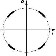
The LO phase noise also corrupts phase-modulated signals in the process of upconversion or downconversion. Since the phase noise is indistinguishable from phase (or frequency) modulation, the mixing of the signal with a noisy LO in the TX or RX path corrupts the information carried by the signal. For example, a QPSK signal containing phase noise can be expressed as
![]()
revealing that the amplitude is unaffected by phase noise. Thus, the constellation points experience only random rotation around the origin (Fig. 8.53). If large enough, phase noise and other nonidealities move a constellation point to another quadrant, creating an error.
Figure 8.53 Corruption of a QPSK signal due to phase noise.
8.7.3 Analysis of Phase Noise: Approach I
Oscillator phase noise has been under study for decades [3]–[17], leading to a multitude of analysis techniques in the frequency and time domains. The calculation of phase noise by hand still remains tedious, but simulation tools such as Cadence’s SpectreRF have greatly simplified the task. Nonetheless, a solid understanding of the mechanisms that give rise to phase noise proves essential to oscillator design. In this section, we analyze these mechanisms. In particular, we must answer two important questions: (1) how much and at what point in an oscillation cycle does each device “inject” noise? (2) how does the injected noise produce phase noise in the output voltage waveform?
Q of an Oscillator
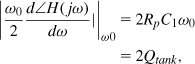
In Chapters 2 and 7, we derived various expressions for the Q of an LC tank. We know intuitively that a high Q signifies a sharper resonance, i.e., a higher selectivity. Another definition of the Q that is especially well-suited to oscillators is illustrated in Fig. 8.55. Here, the circuit is viewed as a feedback system and the phase of the open-loop transfer function, φ(ω), is examined at the resonance frequency, ω0. The “open-loop” Q is defined as
![]()
Figure 8.55 Definition of open-loop Q.
This definition offers an interesting insight if we recall that for steady oscillation, the total phase shift around the loop must be 360° (or zero). Suppose the noise injected by the devices attempts to deviate the frequency from ω0. From Fig. 8.55, such a deviation translates to a change in the total phase shift around the loop, violating Barkhausen’s criterion and forcing the oscillator to return to ω0. The larger the slope of φ(jω), the greater is this “restoration” force; i.e., oscillators with a high open-loop Q tend to spend less time at frequencies other than ω0. In Problem 8.10, we prove that this definition of Q coincides with our original definition, Q = Rp/(Lω), for a CS stage loaded by a second-order tank.
Solution:
![]()
![]()
Figure 8.56 Open-loop model of a cross-coupled oscillator.
Differentiating both sides with respect to ω, calculating the result at ![]() , and multiplying it by ω0/2, we obtain
, and multiplying it by ω0/2, we obtain
While the open-loop Q indicates how much an oscillator “rejects” the noise, the phase noise depends on three other factors as well: (1) the amount of noise that different devices inject, (2) the point in time during a cycle at which the devices inject noise (some parts of the waveform are more sensitive than others), and (3) the output voltage swing (carrier power). We elaborate on these as we analyze phase noise.
Noise Shaping in Oscillators
As our first step toward formulating the phase noise, we wish to understand what happens if noise is injected into an oscillatory circuit. Employing the feedback model, we represent the noise as an additive term [Fig. 8.57(a)] and write
![]()
Figure 8.57 (a) Oscillator model, (b) noise shaping in oscillator.

In the vicinity of the oscillation frequency, i.e., at ω = ω0 + Δω, we can approximate H(jω) with the first two terms in its Taylor series:
![]()
If H(jω0) = −1 and ΔωdH/dω ![]() 1, then Eq. (8.100) reduces to
1, then Eq. (8.100) reduces to
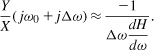
In other words, as shown in Fig. 8.57(b), the noise spectrum is “shaped” by
To determine the shape of |dH/dω|2, we write H(jω) in polar form, H(jω) = |H| exp(jφ) and differentiate with respect to ω,
![]()
It follows that
![]()
This equation leads to a general definition of Q [4], but we limit our study here to simple LC oscillators. Note that (a) in an LC oscillator, the term |d|H|/dω|2 is much less than |dφ/dω|2 in the vicinity of the resonance frequency, and (b) |H| is close to unity for steady oscillations. The right-hand side of Eq. (8.105) therefore reduces to |dφ/dω|2, yielding
From (8.95),
![]()
Known as “Leeson’s Equation” [3], this result reaffirms our intuition that the open-loop Q signifies how much the oscillator rejects the noise.
In Problem 8.11, we prove that, if the feedback path has a transfer function G(s) (Fig. 8.59), then
![]()
where the open-loop Q is given by
![]()
Figure 8.59 Noise shaping in a general oscillator.

Linear Model
The foregoing development suggests that the total noise at the output of an oscillator can be obtained according to a number of transfer functions similar to Eq. (8.107) from each noise source to the output. Such an approach begins with a small-signal (linear) model and can account for some of the nonidealities [4]. However, the small-signal model may ignore some important effects, e.g., the noise of the tail current source, or face other difficulties. The following example illustrates this point.
Compute the total noise injected to the differential output of the cross-coupled oscillator when the transistors are in equilibrium. Note that the two-sided spectral density of the drain current noise is equal to ![]() .
.
Solution:
![]()
where R = (−2/gm)||Rp. Since In1 and In2 are uncorrelated, ![]() and hence
and hence
![]()
Figure 8.60 (a) Circuit for finding Norton noise equivalent of cross-coupled pair, (b) overall model of oscillator.
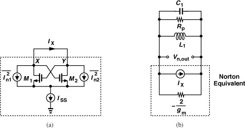
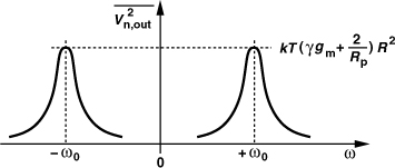
Figure 8.61 plots the spectrum of ![]() . Unfortunately, this result contradicts Leeson’s equation. As explained in Section 8.3, gm is typically quite higher than 2/Rp and hence R ≠ ∞. Thus, as ω → ω0,
. Unfortunately, this result contradicts Leeson’s equation. As explained in Section 8.3, gm is typically quite higher than 2/Rp and hence R ≠ ∞. Thus, as ω → ω0, ![]() does not go to infinity. This is another difficulty arising from the linear model.
does not go to infinity. This is another difficulty arising from the linear model.
Figure 8.61 Output spectrum due to transistor noise currents.
Conversion of Additive Noise to Phase Noise
The result expressed by (8.107) and exemplified by (8.111) yields the total noise that is added to the oscillation waveform at the output. We must now determine how and to what extent additive noise corrupts the phase.
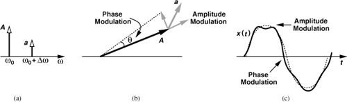
Let us begin with the simple case depicted in Fig. 8.62(a). The carrier appears at ω0 and the additive noise in a 1-Hz bandwidth centered at ω0 + Δω is modeled by an impulse. In the time domain, the overall waveform is x(t) = A cos ω0t + a cos(ω0 + Δω)t where a ![]() A. Intuitively, we expect the additive component to produce both amplitude and phase modulation. To understand this point, we represent the carrier by a phasor of magnitude A that rotates at a rate of ω0 [Fig. 8.62(b)]. The component at ω0 + Δω adds vectorially to the carrier, i.e., it appears as a small phasor at the tip of the carrier phasor and rotates at a rate of ω0 + Δω. At any point in time, the small phasor can be expressed as the sum of two other phasors, one aligned with A and the other perpendicular to it. The former modulates the amplitude and the latter, the phase. Figure 8.62(c) illustrates the behavior in the time domain.
A. Intuitively, we expect the additive component to produce both amplitude and phase modulation. To understand this point, we represent the carrier by a phasor of magnitude A that rotates at a rate of ω0 [Fig. 8.62(b)]. The component at ω0 + Δω adds vectorially to the carrier, i.e., it appears as a small phasor at the tip of the carrier phasor and rotates at a rate of ω0 + Δω. At any point in time, the small phasor can be expressed as the sum of two other phasors, one aligned with A and the other perpendicular to it. The former modulates the amplitude and the latter, the phase. Figure 8.62(c) illustrates the behavior in the time domain.
Figure 8.62 (a) Addition of a small sideband to a sinusoid, (b) phasor diagram showing both AM and PM, (c) time-domain waveform.
In order to compute the phase modulation resulting from a small sinusoid at ω0 + Δω, we make two important observations. First, as described in Chapter 3, the spectrum of Fig. 8.62(a) can be written as the sum of an AM signal and an FM signal. Second, the phase of the overall signal is obtained by applying the composite signal to a hard limiter, i.e., a circuit that clips the amplitude and hence removes AM. From Chapter 3, the output of the limiter can be written as

We recognize the phase component, (2a/A) sin Δωt, as simply the original additive component at ω0 + Δω, but translated down by ω0, shifted by 90°, and normalized to A/2. We therefore expect that narrowband random additive noise in the vicinity of ω0 results in a phase whose spectrum has the same shape as that of the additive noise but translated by ω0 and normalized to A/2.
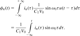
This conjecture can be proved analytically. We write x(t) = A cos ω0t + n(t), where n(t) denotes the narrowband additive noise (voltage or current). It can be proved that narrowband noise in the vicinity of ω0 can be expressed in terms of its quadrature components [9]:
![]()
where nI(t) and nQ(t) have the same spectrum, which [for real n(t)] is equal to the spectrum of n(t) but translated down by ω0 (Fig. 8.63) and doubled in spectral density. It follows that
![]()
Figure 8.63 Narrowband noise and spectrum of its quadrature components.
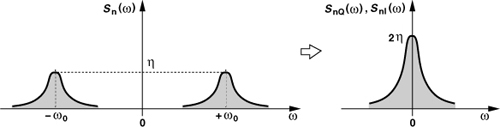
Expressing Eq. (8.115) in polar form, we have
![]()
Since nI(t), nQ(t) ![]() A, the phase component is equal to
A, the phase component is equal to
![]()
as postulated previously. It follows that
![]()
Note that A is the peak (not the rms) amplitude of the carrier. In Problem 8.12, we prove that half of the noise power is carried by the AM sidebands and the other half by the PM sidebands.
We are ultimately interested in the spectrum of the RF waveform, x(t), but excluding its AM noise. We have

Thus, the power spectral density of x(t) consists of two impulses at ±ω0, each with a power of A2/4, and SnQ/4 centered around ±ω0. As shown in Fig. 8.64, a spectrum analyzer folds the negative- and positive-frequency contents. After the folding, we normalize the phase noise to the total carrier power, A2/2.
Figure 8.64 Summary of conversion of additive noise to phase noise.
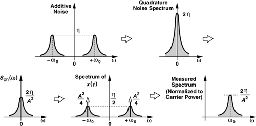
The foregoing development can be summarized as follows (Fig. 8.64). Additive noise around ±ω0 having a two-sided spectral density with a peak of η results in a phase noise spectrum around ω0 having a normalized one-sided spectral density with a peak of 2η/A2, where A is the peak amplitude of the carrier.
Cyclostationary Noise
The derivations leading to Eq. (8.111) have assumed that the noise of each transistor can be represented by a constant spectral density; however, as the transistors experience large-signal excursions, their transconductance and hence noise power varies. Since oscillators perform this noise modulation periodically, we say such noise sources are “cyclostationary,” i.e., their spectrum varies periodically. We begin our analysis with an observation made in Chapter 6 regarding cyclostationary white noise: white noise multiplied by a periodic envelope in the time domain remains white. For example, if white noise is switched on and off with 50% duty cycle, the result is still white but has half the spectral density.
In order to study the effect of cyclostationary noise, we return to the original cross-coupled oscillator and, from Fig. 8.65(a), recognize that (1) when VX reaches a maximum and VY a minimum, M1 turns off, injecting no noise; (2) when M1 and M2 are near equilibrium, they inject maximum noise current, with a total two-sided spectral density of kTγ gm, where gm is the equilibrium transconductance; (3) when VX reaches a minimum and VY a maximum, M1 is on but degenerated by the tail current (while M2 is off), injecting little noise to the output. We therefore conclude that the total noise current experiences an envelope having twice the oscillation frequency and swinging between zero and unity [Fig. 8.65(b)].
Figure 8.65 (a) General cross-coupled oscillator, (b) envelope of transistor noise waveforms.
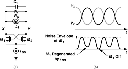
The noise envelope waveform can be determined by simulations, but let us approximate the envelope by a sinusoid, 0.5 cos 2ω0t + 0.5. The reader can show that white noise multiplied by such an envelope results in white noise with three-eighths the spectral density. Thus, we simply multiply the noise contribution of M1 and M2, kTγ gm, by 3/8.
How about the noise of the tanks? We observe that the noise of Rp in Fig. 8.58 is stationary. In other words, the two-sided tank noise contribution is equal to 2kT/Rp (but only half of this value is converted to phase noise).
Time-Varying Resistance
In addition to cyclostationary noise, the time variation of the resistance presented by the cross-coupled pair also complicates the analysis. However, since we have taken a “macroscopic” view of cyclostationary noise and modeled it by an equivalent white noise, we may consider a time average of the resistance as well.
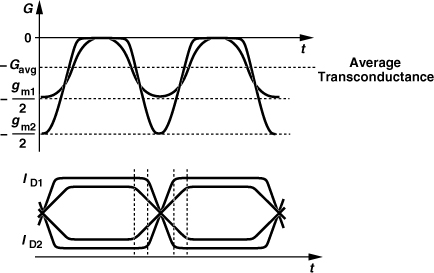
We have noted that the resistance seen between the drains of M1 and M2 in Fig. 8.65(a) periodically varies from −2/gm to nearly infinity. The corresponding conductance, G, thus swings between −gm/2 and nearly zero (Fig. 8.66), exhibiting a certain average, −Gavg. The value of −Gavg is readily obtained as the first term of the Fourier expansion of the conductance waveform.
Figure 8.66 Time variation of conductance of cross-coupled pair.

What can we say about −Gavg? If −Gavg is not sufficient to compensate for the loss of the tank, Rp, then the oscillation decays. Conversely, if −Gavg is more than enough, then the oscillation amplitude grows. In the steady state, therefore, Gavg = 1/Rp. This is a powerful observation: regardless of the transistor dimensions and the value of the tail current, Gavg must remain equal to Rp.
Solution:
Figure 8.67 Effect of increasing tail current on (a) transconductance, and (b) oscillation waveforms.
Phase Noise Computation
We now consolidate our formulations of (a) conversion of additive noise to phase noise, (b) cyclostationary noise, and (c) time-varying resistance. Our analysis proceeds as follows:
1. We compute the average spectral density of the noise current injected by the cross-coupled pair. If a sinusoidal envelope is assumed, the two-sided spectral density amounts to kTγ gm × (3/8), where gm denotes the equilibrium transconductance of each transistor.
2. To this we add the noise current of Rp, obtaining (3/8)kTγ gm + 2kT/Rp.
3. We multiply the above spectral density by the squared magnitude of the net impedance seen between the output nodes. Since Gavg = 1/Rp, the average resistance is infinite, leaving only L1 and C1 in Fig. 8.65(a). That is,
![]()
which, for ω = ω0 + Δω and Δω ![]() ω0, reduces to
ω0, reduces to
![]()
The factor of 3/8 depends on the noise envelope waveform and must be obtained by careful simulations.
4. From Fig. 8.64, we divide this result by A2/2 to obtain the one-sided phase noise spectrum around ω0. Note that in Fig. 8.65(a), A = (4/π)(ISSRp/2) = (2/π)ISS/Rp and Rp = QL1ω0.7 It follows that
![]()
As the tail current and hence the output swings increase, ![]() rises much more sharply than gm, thereby lowering the phase noise (so long as the transistors do not enter the deep triode region).
rises much more sharply than gm, thereby lowering the phase noise (so long as the transistors do not enter the deep triode region).
A closer examination of the cross-coupled oscillator reveals that the phase noise is in fact independent of the transconductance of the transistors [10, 11, 17]. This can be qualitatively justified as follows. Suppose the widths of the two transistors are increased while the output voltage swing and frequency are kept constant. The transistors can now steer their tail current with a smaller voltage swing, thus experiencing sharper current switching (Fig. 8.68). That is, M1 and M2 spend less time injecting noise into the tank. However, the higher transconductance translates to a higher amount of injected noise, as evident from the noise envelope. It turns out that the decrease in the width and the increase in the height of the noise envelope pulses cancel each other, and gm can be simply replaced with 2/Rp in the above equation [10, 11, 17]:
![]()
Figure 8.68 Oscillator waveforms for different transistor widths.

Problem of Tail Capacitance
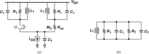
What happens if one of the transistors enters the deep triode region? As depicted in Fig. 8.69(a), the corresponding tank is temporarily connected to the tail capacitance through the on-resistance of the transistor, degrading the Q. Transforming the series combination of Ron and CT to a parallel circuit, we obtain the equivalent network shown in Fig. 8.69(b), where ![]() . If RT is comparable to R1 and each transistor remains in the deep triode region for an appreciable fraction of the period, then the Q degrades significantly. Equivalently, the noise injected by M2 rises considerably [17].
. If RT is comparable to R1 and each transistor remains in the deep triode region for an appreciable fraction of the period, then the Q degrades significantly. Equivalently, the noise injected by M2 rises considerably [17].
Figure 8.69 (a) Oscillator with one transistor in deep triode region, (b) equivalent circuit of the tank.
The key result here is that, as the tail current is increased, the (relative) phase noise continues to decline up to the point where the transistors enter the triode region. Beyond this point, a higher tail current raises the output swing more gradually, but the overall tank Q begins to fall, yielding no significant improvement in the phase noise. Of course, this trend depends on the value of CT and may be pronounced only in some designs. This capacitance may be large due to the parasitics of ISS or it may be added deliberately to shunt the noise of ISS to ground (Section 8.7.5).
8.7.4 Analysis of Phase Noise: Approach II
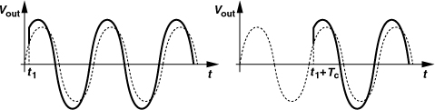
The approach described in this section follows that in [6]. Consider an ideal LC tank that, due to an initial condition, produces a sinusoidal output [Fig. 8.70(a)]. During the oscillation, L1 and C1 exchange the initial energy, with the former carrying the entire energy at the zero crossings and the latter, at the peaks. Let us assume that the circuit begins with an initial voltage of V0 across the capacitor. Now, suppose an impulse of current is injected into the oscillating tank at the peak of the output voltage [Fig. 8.70(b)], producing a voltage step across C1. If8
![]()
then the additional energy gives rise to a larger oscillation amplitude:
![]()
Figure 8.70 (a) Ideal tank with a current impulse, (b) effect of impulse injection at peak of waveform, (c) effect of impulse injection at zero crossing of waveform.

The key point here is that the injection at the peak does not disturb the phase of the oscillation (as shown in the example below).
Next, let us assume the impulse of current is injected at a zero crossing point. A voltage step is again created but leading to a phase jump [Fig. 8.70(c)]. Since the voltage jumps from 0 to I1/C1, the phase is disturbed by an amount equal to sin−1[I1/(C1V0)]. We therefore conclude that noise creates only amplitude modulation if injected at the peaks and only phase modulation if injected at the zero crossings.

The foregoing observations suggest the need for a method of quantifying how and when each source of noise in an oscillator “hits” the output waveform. While the transistors turn on and off, a noise source may only appear near the peaks of the output voltage, contributing negligible phase noise, whereas another may hit the zero crossings, producing substantial phase noise. To this end, we define a linear, time-variant system from each noise source to the output phase. The linearity property is justified because the noise levels are very small, and the time variance is necessary to capture the effect of the time at which the noise appears at the output.
For a linear, time-variant system, the convolution property holds, but the impulse response varies with time. Thus, the output phase in response to a noise n(t) is given by
![]()
where h(t, τ) is the time-variant impulse response from n(t) to φ(t). In an oscillator, h(t, τ) varies periodically: as illustrated in Fig. 8.72, a noise impulse injected at t = t1 or integer multiples of the period thereafter produces the same phase change. Now, the task of output phase noise calculation consists of computing h(t, τ) for each noise source and convolving it with the noise waveform. The impulse response, h(t, τ), is called the “impulse sensitivity function” (ISF) in [6].
Figure 8.72 Periodic impulse response in an oscillator.
Solution:
![]()
![]()
![]()
Figure 8.73 Waveforms for computation of phase impulse response of a tank.

![]()
Interestingly, φout is not a linear function of ΔV in general. But, if ΔV ![]() V0, then
V0, then
![]()
![]()
Let us now return to Eq. (8.127) and determine how the convolution is carried out. It is instructive to begin with a linear, time-invariant system. A given input, x(t), can be approximated by a series of time-domain impulses, each carrying the energy of x(t) in a short time span [Fig. 8.74(a)]:
![]()
Figure 8.74 Convolution in a (a) time-invariant, and (b) time-variant linear system.
Each impulse produces the time-invariant impulse response of the system at tn. Thus, y(t) consists of time-shifted replicas of h(t), each scaled in amplitude according to the corresponding value of x(t):
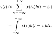
Now, consider the time-variant system shown in Fig. 8.74(b). In this case, the time-shifted versions of h(t) may be different, and we denote them by h1(t), h2(t), ..., hn(t), with the understanding that hj(t) is the impulse response in the vicinity of tj. It follows that
![]()
How do we express these impulse responses as a continuous-time function? We simply write them as h(t, τ), where τ is the specific time shift. For example, h1(t) = h(t, 1 ns), h2(t) = h(t, 2 ns), etc. Thus,

Solution:
![]()

Figure 8.75 (a) Equivalent system for conversion of g(t) to φn(t), (b) resulting phase noise spectrum.
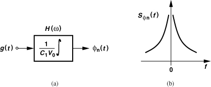
Figure 8.76 Summary of conversion of injected noise to phase noise around the carrier.
The reader may find the foregoing example confusing: if the lossless tank with its nonzero initial condition is viewed as an oscillator with infinite Q, why is the phase noise not zero? This confusion is resolved if we recognize that, as Q → ∞, the width and bias current of the transistor needed to sustain oscillation become infinitesimally small. The transistor thus injects nearly zero noise; i.e., if in(t) represents transistor noise, Si(f) approaches zero.
Effect of Flicker Noise
Due to its periodic nature, the impulse response of oscillators can be expressed as a Fourier series:
![]()
where a0 is the average (or “dc”) value of h(t, τ). In the LC tank studied above, aj = 0 for all j ≠ 1, but in general this may not be true. In particular, suppose a0 ≠ 0. Then, the corresponding phase noise in response to an injected noise in(t) is equal to
From Example 8.35, the integration is equivalent to a transfer function of (jω)−1 and hence
![]()
That is, low-frequency components in in(t) contribute phase noise. (Recall that Sφn,a0 is upconverted to a center frequency of ω0.) The key point here is that, if the “dc” value of h(t, τ) is nonzero, then the flicker noise of the MOS transistors in the oscillator generates phase noise. For flicker noise, we employ the gate-referred noise voltage expression given by Sv(f) = [K/(WLCox)]/f and write
![]()
Note that in this case, a0 represents the dc term of the impulse response from the gate voltage of the transistors to the output phase. Since a0 relates to the symmetry of h(t, τ), low upconversion of 1/f noise requires a circuit design that exhibits an odd-symmetric h(t, τ) [6]. However, the 1/f noise of different transistors in the circuit may see different impulse responses, and it may therefore be impossible to minimize the upconversion of all 1/f noise sources. For example, in the circuit of Fig. 8.35, it is possible to make h(t, τ) from the gates of M1-M4 to the output symmetric, but not from the tail current source to the output. As ISS slowly fluctuates, so does the output CM level and hence the oscillation frequency. In general, the phase noise spectrum assumes the shape shown in Fig. 8.77.
Figure 8.77 Phase noise profile showing regions arising from flicker and white noise.
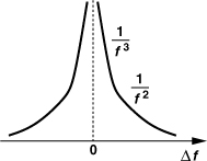
Noise around Higher Harmonics
Let us now turn our attention to the remaining terms in Eq. (8.144). As mentioned in Example 8.35, a1 cos(ω0t + φ1) translates noise frequencies around ω0 to the vicinity of zero and into phase noise. By the same token, am cos(mω0t + φj) converts noise components around mω0 in in(t) to phase noise. Figure 8.78 illustrates this behavior [6].
Figure 8.78 Conversion of various noise components to phase noise.
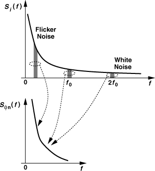
Cyclostationary Noise
We must also incorporate the effect of cyclostationary noise. As explained in Section 8.7.3, such noise can be viewed as stationary noise, n(t), multiplied by a periodic envelope, e(t). Equation (8.138) can thus be written as
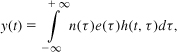
implying that e(t)h(t, τ) can be viewed as an “effective” impulse response [6]. In other words, the effect of n(t) on phase noise ultimately depends on the product of the cyclostationary noise envelope and h(t, τ).
This approach to phase noise analysis generally requires that both the noise envelope and the impulse response be determined from multiple simulations for each device. Design optimization may therefore prove a lengthy task.
Each of the two analysis approaches described thus far imparts its own insights and finds its own utility in circuit design. However, there are other phase noise mechanisms that can be better understood by other analysis techniques. The next section is an example.
8.7.5 Noise of Bias Current Source
Oscillators typically employ a bias current source so as to minimize sensitivity to the supply voltage and noise therein. We wish to study the phase noise contributed by this current source. Figure 8.79 summarizes the tail-related noise mechanisms studied here.
Figure 8.79 Tail noise mechanisms in cross-coupled oscillator.

Consider the topology shown in Fig. 8.80(a), where In models the noise of ISS, including flicker noise near zero frequency, thermal noise around the oscillation frequency, ω0, thermal noise around 2ω0, etc. We also recognize that M1 and M2 are periodically turned on and off, thus steering (commutating) ISS + In and hence operating as a mixer. In other words, the two circuits shown in Fig. 8.80(b) are similar, and the differential current injected by M1 and M2 into the tanks can be viewed as the product of ISS + In and a square wave toggling between −1 and + 1 (for large swings).
Figure 8.80 (a) Oscillator with noisy tail current source, (b) circuit viewed as a mixer.
We now examine the effect of different noise frequencies upon the performance of the oscillator in Fig. 8.80(a). The flicker noise in In slowly varies the bias current and hence the output voltage swing (4ISSRp/π), introducing amplitude modulation. We therefore postulate that the flicker noise produces negligible phase noise. As explained later, this is not true in the presence of voltage-dependent capacitances at the output nodes (e.g., varactors), but we neglect the effect of flicker noise for now.
How about the noise around ω0? This noise component is mixed with the harmonics of the square wave, ω0, 3ω0, 5ω0,..., landing at 0, 2ω0, 4ω0,.... Thus, this component is negligible.
The noise around 2ω0, on the other hand, markedly impacts the performance [12, 7]. As illustrated in Fig. 8.81(a), a noise component slightly below 2ω0 is mixed with the first and third harmonics of the square wave, thereby falling at slightly below and above ω0 but with different amplitudes and polarities. To determine whether these components produce AM or FM, we express the oscillator output as cos ω0t and its third harmonic as (−1/3) cos(3ω0t). For a tail current noise component, I0 cos(2ω0 − Δω)t, the differential output current of M1 and M2 emerges as
Figure 8.81 (a) Translation of tail noise around 2ω0 to sidebands around ω0, (b) separation of PM and AM components.
As explained in Chapter 3, two equal cosine sidebands having opposite signs surrounding a cosine carrier represent FM. In the above equation, however, the two sidebands have unequal magnitudes, creating some AM as well. Writing (I0/2) cos(ω0 − Δω)t = (I0/6) cos(ω0 − Δω)t + (I0/3) cos(ω0 − Δω)t and extracting from the second term its PM components [Fig. 8.81(b)] as (I0/6) cos(ω0 − Δω)t − (I0/6) cos(ω0 + Δω)t, we obtain the overall PM sidebands:
![]()
The proportionality factor is related to the conversion gain of the mixing action, as illustrated by the following example.
To obtain the phase noise in the output voltage, (1) the current sidebands computed in the above example must be multiplied by the impedance of the tank at a frequency offset of ±Δω, and (2) the result must be normalized to the oscillation amplitude. Note that the current components see the lossless impedance of the tank once they are injected into the output nodes because the average negative conductance presented by M1 and M2 cancels the loss. This impedance is given by −j/(2C1Δω) if Δω ![]() ω0. Thus, the relative phase noise can be expressed as
ω0. Thus, the relative phase noise can be expressed as

The thermal noise near higher even harmonics of ω0 plays a similar role, producing FM sidebands around ω0. It can be shown that the summation of all of the sideband powers results in the following phase noise expression due to the tail current source [8, 10]:
![]()
Let us now consider the noise of the top current source in Fig. 8.30(a). We wish to formulate the frequency modulation resulting from this noise. Suppose IDD contains a noise current in(t). As calculated in Example 8.16, in(t) produces a common-mode voltage change of
![]()
This change is indistinguishable from an equal but opposite change in the control voltage, Vcont. As explained in Section 8.10, the output waveform can be expressed as
![]()
where the second term in the square brackets is the resulting phase noise, φn(t). If φn(t) ![]() 1 rad, then
1 rad, then
![]()
We recognize that low-frequency components in in(t) are upconverted to the vicinity of ω0. In particular, as shown in Fig. 8.82, 1/f noise components in in(t) experience a transfer function of [KVCO/(2gm)](1/s), producing
![]()
Figure 8.82 Equivalent transfer function for conversion of top bias current to phase noise.

AM/PM Conversion
Let us summarize our findings thus far. In the tail-biased oscillator (and in the top-biased oscillator), the noise near zero frequency introduces amplitude modulation, whereas that near even harmonics of ω0 leads to phase noise. [In the top-biased oscillator, low-frequency noise in the current source also modulates the output CM level, producing phase noise (Example 8.16).]
The amplitude modulation resulting from the bias current noise does translate to phase noise in the presence of nonlinear capacitances in the tanks [13, 14]. To understand this point, we return to our AM/PM modulation study in Chapter 2 and make the following observations. Since the varactor capacitance varies periodically with time, it can be expressed as a Fourier series:
![]()
where Cavg denotes the “dc” value. If noise in the circuit modulates Cavg, then the oscillation frequency and phase are also modulated. We must therefore determine under what conditions the tail noise, i.e., the output AM noise, modulates Cavg.
Consider the tank shown in Fig. 8.83(a), and first assume that the voltage dependence of C1 is odd-symmetric around the vertial axis, e.g., C1 = C0(1 + αV). In this case, Cavg is independent of the signal amplitude because the capacitance spends equal amounts of time above and below C0 [Fig. 8.83(b)]. The average tank resonance frequency is thus constant and no phase modulation occurs.
Figure 8.83 (a) Tank driven by an RF current course, (b) effect of AM on average capacitance for a C/V characteristic that is symmetric around vertical axis, (c) effect of AM on average capacitance for a C/V characteristic that is asymmetric around vertical axis.

The above results change if C1 exhibits even-order voltage dependence, e.g., C1 = C0(1 + α1V + α2V2). Now, the capacitance changes more sharply for negative or positive voltages, yielding an average that depends on the current amplitude [Fig. 8.83(c)]. We therefore observe that, in an oscillator employing such a tank, slow modulation of the amplitude varies the average tank resonance frequency and hence the frequency of oscillation. The phase noise resulting from the low-frequency bias current noise is computed in [13]. We study a simplified case in Problem 8.13.
It is important to note that the tail current in Fig. 8.35 introduces phase noise via three distinct mechanisms: (1) its flicker noise modulates the output CM level and hence the varactors; (2) its flicker noise produces AM at the output and hence phase noise through AM/PM conversion; (3) its thermal noise at 2ω0 gives rise to phase noise.
8.7.6 Figures of Merit of VCOs
Our studies in this chapter point to direct trade-offs among the phase noise, power dissipation, and tuning range of VCOs. For example, as explained in Chapter 7, varactors themselves suffer from a trade-off between their capacitance range and their Q. We also recall from Leeson’s equation, Eq. (8.107), that phase noise rises with the oscillation frequency if the Q does not increase proportionally.
A figure of merit (FOM) that encapsulates some of these trade-offs is defined as
![]()
where the phase noise is multiplied by the square of the offset frequency at which it is measured so as to perform normalization. Attention must be paid to the unit of phase noise (noise power normalized to carrier power) in this expression. Note that the product of power dissipation and phase noise has a unit of W/Hz. Another FOM that additionally represents the trade-offs with the tuning range is
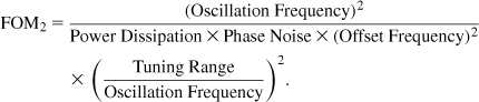
State-of-the-art CMOS VCOs in the range of several gigahertz achieve an FOM2 around 190 dB. In general, the phase noise in the above expressions refers to the worst-case value, typically at the the highest oscillation frequency. Also, note that these FOMs do not account for the load driven by the VCO.
8.8 Design Procedure
Following our study of tuning techniques and phase noise issues, we now describe a procedure for the design of LC VCOs. We focus on the topology shown in Fig. 8.25(a) and assume the following parameters are given: the center frequency, ω0, the output voltage swing, the power dissipation, and the load capacitance, CL. Even though some of these parameters may not be known at the outset, it is helpful to select some reasonable values and iterate if necessary. Of course, the output swing must be chosen so as not to stress the transistors.
The procedure consists of six steps:
1. Based on the power budget and hence the maximum allowable ISS, select the tank parallel resistance, Rp, so as to obtain the required voltage swing, (4/π)ISSRp.
2. Select the smallest inductor value that yields a parallel resistance of Rp at ω0, i.e., find the inductor with the maximum Q = Rp/(Lω0). This, of course, relies on detailed modeling and characterization of inductors in the technology at hand (Chapter 7). Denote the capacitance contributed by the inductors to each node by Cp.
3. Determine the dimensions of M1 and M2 such that they experience nearly complete switching with the given voltage swings. To minimize their capacitance contributions, choose minimum channel length for the transistors.
4. Noting that the transistor, inductor, and load capacitances amount to a total of CGS + 4CGD + CDB + Cp + CL at each output node, calculate the maximum varactor capacitance, Cvar,max, that can be added to reach the lower end of the tuning range, ωmin; e.g., ωmin = 0.9ω0:
![]()
5. Using proper varactor models, determine the minimum capacitance of such a varactor, Cvar,min, and compute the upper end of the tuning range,
![]()
6. If ωmax is quite higher than necessary, increase Cvar,max in Eq. (8.162) so as to center the tuning range around ω0.
The above procedure yields a design that achieves the maximum tuning range subject to known values of ω0, the output swing, the power dissipation, and CL. If the varactor Q is high enough, such a design also has the highest tank Q. At this point, we calculate or simulate the phase noise for different frequencies across the tuning range. If the phase noise rises significantly at ωmin or ωmax, then the tuning range must be reduced, and if it is still excessively high, the design procedure must be repeated with a higher power budget. In applications requiring a low phase noise, a multitude of different VCO topologies must be designed and simulated so as to obtain a solution with an acceptable performance.
We carry out the detailed design of a 12-GHz VCO for 11a/g applications in Chapter 13.
Solution:
Doubling the power budget can be viewed as (a) placing two identical oscillators in parallel [Fig. 8.84(a)] or (b) scaling all of the components in an oscillator by a factor of 2 [Fig. 8.84(b)]. In this scenario, the output voltage swing and the tuning range remain unchanged (why?), but the phase noise power falls by a factor of two (3 dB). This is because in Eq. (8.124), Rp is doubled and ![]() is quadrupled.
is quadrupled.
Figure 8.84 Scaling of oscillator by (a) placing two instances in parallel, (b) scaling each component.
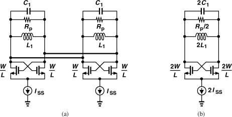
8.8.1 Low-Noise VCOs
A great deal of effort has been expended on relaxing the trade-offs among phase noise, power dissipation, and tuning range of VCOs. In this section, we study several examples.
In order to reduce the phase noise due to flicker noise, the generic cross-coupled oscillator can incorporate PMOS transistors rather than NMOS devices. Figure 8.85 depicts the PMOS counterparts of the circuits shown in Figs. 8.25(a) and 8.30(a). Since PMOS devices exhibit substantially less flicker noise, the close-in phase noise of these oscillators is typically 5 to 10 dB lower. The principal drawback of these topologies is their limited speed, an issue that arises only as frequencies exceeding tens of gigahertz are sought.
Figure 8.85 (a) Tail-biased and (b) bottom-biased PMOS oscillators.

As explained in Section 8.7.5, the noise current at 2ω0 in the tail current source translates to phase noise around ω0. This and higher noise harmonics can be removed by a capacitor as shown in Fig. 8.86(a). However, if M1 and M2 enter the deep triode region during oscillation, then two effects raise the phase noise: (1) the on-resistance of each transistor now degrades the Q of the tank [Fig. 8.69(a)] [16], and (2) the impulse response (ISF) from the noise of each transistor to the output phase becomes substantially larger [17]. This issue can be resolved by means of two techniques. If operation in the triode region must be avoided but large output swings are desired, capacitive coupling can be inserted in the loop [Fig. 8.86(b)]. Here, Vb is chosen so that the peak voltage at the gate of each transistor does not exceed its minimum drain voltage by more than one threshold. A Class-C oscillator similar to this topology is described in [17].
Figure 8.86 (a) Use of capacitor to shunt tail noise, (b) use of ac coupling to avoid operation in deep triode region.

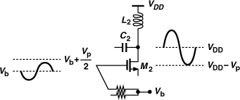
The bias voltage, Vb, in Fig. 8.86(b) must remain high enough to provide sufficient VGS for the cross-coupled transistors and headroom for the tail current source. Consequently, the output swings may still be severely limited. In Problem 8.14, we show that the peak swing does not exceed approximately VDD − 2(VGS − VTH). This is obtained only if the capacitive attenuation is so large as to yield a negligible gate swing, requiring a high gm.
The second approach is to allow M1 and M2 in Fig. 8.86(a) to enter the triode region but remove the effect of the tail capacitance at 2ω0. Illustrated in Fig. 8.88 [16], the idea is to insert inductor LT in series with the tail node and choose its value such that it resonates with the parasitic capacitance, CB, at 2ω0. The advantage of this topology over that in Fig. 8.86(b) is that it affords larger swings. The disadvantage is that it employs an additional inductor and requires tail tuning for broadband operation.
Figure 8.88 Use of tail resonance to avoid tank Q degradation in deep triode region.
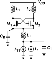
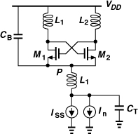
8.9 LO Interface
Each oscillator in an RF system typically drives a mixer and a frequency divider, experiencing their input capacitances. Moreover, the LO output common-mode level must be compatible with the input CM level of these circuits. We study this compatibility issue here.
The output CM level of the oscillators studied in this chapter is around VDD, VDD/2, or zero [for the PMOS implementation of Fig. 8.85(a)]. On the other hand, the required input CM level of the mixers studied in Chapter 6 is somewhat higher than VDD/2 for active NMOS topologies or around VDD (zero) for passive NMOS (PMOS) realizations. Figure 8.90 illustrates some of the LO/mixer combinations, suggesting that dc coupling is possible in only some cases.
Figure 8.90 LO/mixer interface examples.
We consider two approaches to providing CM compatibility. Shown in Fig. 8.91(a), the first employs capacitive coupling and selects Vb such that M1 and M2 do not enter the triode region at the peak of the LO swing. Resistor R1 must be large enough to negligibly degrade the Q of the oscillator tanks. Capacitor C1 may be chosen 5 to 10 times Cin to avoid significant LO attenuation. However, active mixers typically operate with only moderate LO swings, whereas the oscillator output swing may be quite larger so as to reduce its phase noise. Thus, C1 may be chosen to attenuate the LO amplitude. For example, if C1 = Cin, an attenuation factor of 2 results and the capacitance presented to the LO falls to C1Cin/(C1 + Cin) = Cin/2, a useful attribute afforded by active mixers.
Figure 8.91 Use of (a) capacitive coupling, (b) a buffer between LO and mixer.
The second approach to CM compatibility interposes a buffer between the LO and the mixer. In fact, if the mixer input capacitance excessively loads the LO, or if long, lossy interconnects appear in the layout between the LO and the mixer, then such a buffer proves indispensable. Depicted in Fig. 8.91(b) is an example, where an inductively-loaded differential pair serves as a buffer, providing an output CM level equal to VDD − I1R1. This value can be chosen to suit the LO port of the mixer. The drawback of this approach stems from the use of additional inductors and the resulting routing complexity.
Similar considerations apply to the interface between an oscillator and a frequency divider. For example, in Fig. 8.92(a), the divider input CM level must be well below VDD to ensure the current-steering transistors M1 and M2 do not enter the deep triode region (Chapter 10). As another example, some dividers require a rail-to-rail input [Fig. 8.92(b)], and possibly capacitive coupling.
Figure 8.92 LO/divider interface for (a) current-steering and (b) rail-to-rail operation.
8.10 Mathematical Model of VCOs
Our definition of voltage-controlled oscillators in Section 8.5 relates the output frequency to the control voltage by a linear, static equation, ωout = ω0 + KVCOVcont. But, how do we express the output in the time domain? To this end, we must reexamine our understanding of frequency and phase.

![]()
Solution:
![]()
Figure 8.94 (a) Frequency-modulated sinusoid, (b) incorrect definition of phase, (c) corresponding output waveform.
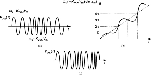
Let us now consider an unmodulated sinusoid, V1(t) = V0 sin ω1t. Called the “total phase,” the argument of the sine, ω1t, varies linearly with time in this case, exhibiting a slope of ω1 [Fig. 8.93(a)]. We say the phase “accumulates” at a rate of ω1. In other words, if ω1 is increased to ω2, then the phase accumulates faster, crossing multiples of π at a higher rate. It is therefore plausible to define the instantaneous frequency as the time derivative of the phase:
![]()
Conversely,
![]()
The initial phase, φ0, is usually unimportant and assumed zero hereafter. Since a VCO exhibits an output frequency given by ω0 + KVCOVcont, we can express its output waveform as
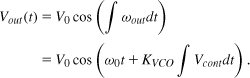
Comparing this result with that in Chapter 3, we recognize that a VCO is simply a frequency modulator. For example, the narrowband FM approximation holds here as well. Note the difference between Eqs. (8.167) and (8.172).
Solution:
![]()
![]()
Figure 8.95 (a) Frequency modulation by a square wave, (b) resulting spectrum.
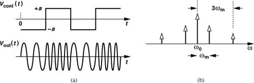
If 4KVCOa/(πωm) ![]() 1 rad, then the narrowband FM approximation applies:
1 rad, then the narrowband FM approximation applies:
![]()
In the analysis of phase-locked frequency synthesizers (Chapter 10), we are concerned with only the second term in the argument of Eq. (8.172). Called the “excess phase,” this term represents an integrator behavior for the VCO. In other words, if the quantity of interest at the output of the VCO is the excess phase, φex, then
![]()
and hence
![]()
The important observation here is that the output frequency of a VCO (almost) instantaneously changes in response to a change in Vcont, whereas the output phase of a VCO takes time to change and “remembers” the past.
8.11 Quadrature Oscillators
In our study of transceiver architectures in Chapter 4, we observed the need for quadrature LO phases in downconversion and upconversion operations. We also noted that flipflop-based divide-by-two circuits generate quadrature phases, but they restrict the maximum LO frequency. In applications where dividers do not offer sufficient speed, we may employ polyphase filters or quadrature oscillators instead. In this section, we study the latter.
8.11.1 Basic Concepts
Two identical oscillators can be “coupled” such that they operate in-quadrature. We therefore begin our study with the concept of coupling (or injecting) a signal to an oscillator. Figure 8.96 depicts an example, where the input voltage is converted to current and injected into the oscillator. The differential pair is a natural means of coupling because the cross-coupled pair can also be viewed as a circuit that steers and injects current into the tanks. If the two pairs completely steer their respective tail currents, then the “coupling factor” is equal to I1/ISS.10 This topology also exemplifies “unilateral” coupling because very little of the oscillator signal couples back to the input. By contrast, if implemented by, say, two capacitors tied between Vin and the oscillator nodes, the coupling is bilateral.
Figure 8.96 Unilateral injection into an oscillator.
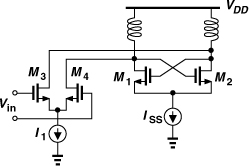
Let us now consider two identical oscillators that are unilaterally coupled. Shown in Fig. 8.97 are two possibilities, with “in-phase” and “anti-phase” coupling. The coupling factors have the same sign in the former and opposite signs in the latter. We analyze these topologies using both the feedback model and the one-port model of the oscillators. Note that the tuning techniques described earlier in this chapter apply to these topologies as well.
Figure 8.97 In-phase and anti-phase coupling of two oscillators.
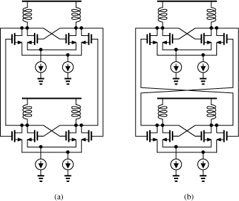
Feedback Model
The circuits of Fig. 8.97 can be mapped to two coupled feedback oscillators as shown in Fig. 8.98, where |α1| = |α2| and the sign of α1α2 determines in-phase or anti-phase coupling [18]. The output of the top adder is equal to α1Y − X, yielding
![]()
Figure 8.98 Feedback model of quadrature oscillator.

Similarly, the bottom oscillator produces
![]()
Multiplying both sides of (8.178) by α2X and both sides of (8.179) by α1Y and subtracting the results, we have
![]()
As explained below, 1 + H(s) ≠ 0 at the oscillation frequency, and hence
![]()
If α1 = α2 (in-phase coupling), then X = ±Y, i.e., the two oscillators operate with a zero or 180° phase difference.
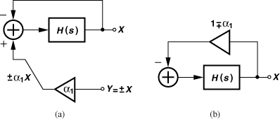
The in-phase operation is not particularly useful as the two oscillators can be simply merged into one (as in Fig. 8.84). On the other hand, if α1 = − α2 (anti-phase coupling), then Eq. (8.181) yields
![]()
i.e., the outputs bear a phase difference of + 90° or −90°. In this case, Eq. (8.182) is revised to
![]()
One-Port Model
It is possible to gain additional insight through the use of the one-port model for each oscillator. A single oscillator experiencing unilateral coupling can be represented as shown in Fig. 8.100(a), where Gm denotes the transconductance of the coupling differential pair (M3 and M4 in Fig. 8.96), ZT the tank impedance, and −RC the negative resistance provided by the cross-coupled pair. Two identical coupled oscillators are therefore modeled as depicted in Fig. 8.100(b), where the sign of Gm1Gm2 determines in-phase or anti-phase coupling.
Figure 8.100 (a) One-port oscillator model with injection, (b) model of coupled oscillators.
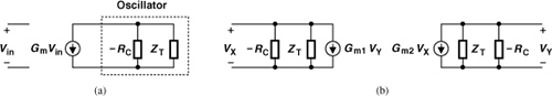
The parallel combination of ZT and −RC is given by −ZTRC/(ZT − RC), yielding
![]()
![]()
Multiplying both sides of (8.186) by VX and both sides of (8.187) by VY and subtracting the results, we have
![]()
Since the parallel combination of ZT and −RC cannot be zero,
![]()
implying that, if Gm1 = − Gm2, then the two oscillators operate in quadrature. Since each oscillator receives energy from the other, the startup condition need not be as stringent as ZT(s = ω0) = RC (Problem 8.15).
8.11.2 Properties of Coupled Oscillators
Unilaterally-coupled oscillators exhibit interesting attributes. Let us consider the case of in-phase coupling as a starting point. As shown in Fig. 8.101, we construct a phasor diagram of the circuit’s voltages and currents. This is accomplished by noting that (1) VA and VB are 180° out of phase, and so are VC and VD, and (2) the drain current of each transistor is aligned with its gate voltage phasor. Thus, the total current flowing through ZA is equal to the sum of the ID1 and ID3 phasors, altering the startup condition according to Eq. (8.182).
Figure 8.101 Phasor diagrams for in-phase coupling.
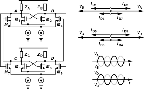
Can the circuit operate with ID3 opposing ID1, i.e., with VC = − VB and VD = − VA? In other words, which one of the solutions, X = + Y or X = − Y in Eq. (8.181), does the circuit select? From Eq. (8.182), VC = − VB is equivalent to a lower loop gain and hence a more slowly growing amplitude. The circuit prefers to begin with the ID3 enhancing ID1 (Fig. 8.101), but this phase ambiguity may exist.
We now repeat this study for anti-phase coupling. Since the two differential oscillators operate in quadrature, the voltage and current phasors appear as in Fig. 8.102, with the drain current phasor of each transistor still aligned with its gate voltage phasor. In this case, the total current flowing through each tank consists of two orthogonal phasors; e.g., ZA carries ID1 and ID3.
Figure 8.102 Phasor diagrams for anti-phase coupling.

How can the vector sum ID1 + ID3 yield VA? Depicted in Fig. 8.103(a), the resultant, IZA, bears an angle of θ with respect to ID1. Thus, the tank must rotate IZA clockwise by an amount equal to θ as it converts the current to voltage. In other words, the tank impedance must provide a phase shift of θ. This is possible only if the oscillation frequency departs from the resonance frequency of the tanks. As illustrated in Fig. 8.103(b), oscillation occurs at a frequency, ωosc1, such that the tank phase shift reaches θ. From Fig. 8.103(a), the tank must rotate IZA by an amount equal to
![]()
i.e., the necessary rotation is determined by the coupling factor. If ZA = (L1s)||(C1s)−1||Rp, then the phase shift of ZA can be set equal to − tan−1(ID3/ID1) so as to obtain ωosc1:
![]()
Figure 8.103 (a) Vector summation of core and coupling currents, (b) resulting departure from resonance.
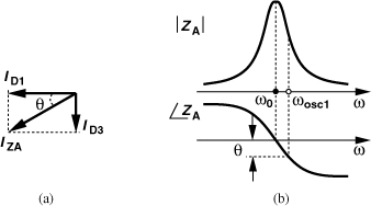
Since ωosc1 − ω0 = Δω ![]() ω0, the argument of tan−1 on the left-hand side can be simplified by writing ωosc1 ≈ ω0 in the numerator and
ω0, the argument of tan−1 on the left-hand side can be simplified by writing ωosc1 ≈ ω0 in the numerator and ![]() in the denominator:
in the denominator:
![]()
We also recognize that tan−1 a ≈ π/2 − 1/a if a ![]() 1 and apply this approximation to the left-hand side:
1 and apply this approximation to the left-hand side:
![]()
![]()
Equation (8.95) yields the same result.
Solution:
![]()
Figure 8.104 (a) Phasors for another possible mode in quadrature oscillators, (b) vector summation of core and coupling currents, (c) resulting departure from resonance.
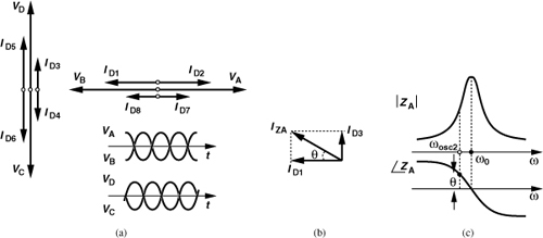
The above example implies that quadrature oscillators may operate at either one of the two frequencies above and below ω0. In fact, Eq. (8.185) also predicts the same results: since H(jω0) is a complex number, oscillation must depart from resonance, and since both 1 + jα1 and 1 − jα1 are acceptable, two solutions above and below resonance exist. Observed in practice as well [19], this property proves a serious drawback. In transient circuit simulations, the oscillator typically operates at ωosc2, exhibiting little tendency to start in the higher mode even with different initial conditions. Nonetheless, it is possible to devise a simulation that reveals the possibility of oscillation at either frequency. This is explained in Appendix A.

It is important to make two observations at this point. (1) The foregoing derivations do not impose a lower bound on the coupling factor, i.e., quadrature operation appears to occur with arbitrarily small coupling factors. Unfortunately, in the presence of mismatches between the natural frequencies of the two oscillators, a small coupling factor may not guarantee “locking.” As a result, each oscillator tends to operate at its own ω0 while it is also “pulled” by the other. The overall circuit exhibits spurious components due to this mutual injection pulling behavior (Fig. 8.106) [20]. To avoid this phenomenon, the coupling factor must be at least equal to [20]
![]()
Figure 8.106 Mutual injection pulling between two oscillators.
We typically choose an α in the range of 0.2 to 0.25. (2) As the coupling factor increases, two issues become more serious: (a) ωosc1 and ωosc2 diverge further, making it difficult to target the desired frequency range if both can occur; and (b) the phase noise of the circuit rises, with the flicker noise of the coupling transistors contributing significantly at low frequency offsets [21, 27]. This can be seen by noting that Δω in Eq. (8.194) is a function of the coupling factor, ID3/ID1, which itself varies slowly with the flicker noise of the coupling transistors and their tail currents [21] (Problem 8.16). It follows that the choice of the coupling factor entails a trade-off between proper, spurious-free operation and phase noise. For a given power dissipation, the phase noise of quadrature oscillators is typically 3 to 5 dB higher [23] than a single oscillator.
The mismatches between the two oscillator cores and the coupling pairs result in phase and amplitude mismatch between the quadrature outputs. These effects are studied in [22, 24].
8.11.3 Improved Quadrature Oscillators
A number of quadrature oscillator topologies have been proposed that alleviate the tradeoffs mentioned above. The principal drawback of the generic configuration studied thus far is that the coupling pairs introduce significant phase noise. We therefore postulate that, if the quadrature relationship between the two core oscillators is established by a different means, then phase noise can be reduced.
Consider the two oscillators shown in Fig. 8.107(a) and suppose they are somehow forced to operate in quadrature at a frequency of ωosc. The tail nodes, A and B, thus exhibit periodic waveforms at 2ωosc and 180° out of phase. Conversely, if additional circuitry forces A and B to sustain a phase difference of 180°, then the two oscillators operate in quadrature. Illustrated in Fig. 8.107(b) [25], such circuitry can be simply a 1-to-1 transformer that couples VA to VB and vice versa. The coupling polarity is chosen such that the transformer inverts the voltage at each node and applies it to the other.
Figure 8.107 (a) Two differential oscillators operating in-quadrature, (b) coupling through tails to ensure quadrature operation.
The topology of Fig. 8.107(b) merits several remarks. First, since the coupling pairs used in the generic circuit of Fig. 8.97 are absent, the two core oscillators operate at their tanks’ resonance frequency, ωosc, rather than depart so as to produce additional phase shift. This important attribute means that this approach avoids the frequency ambiguity suggested by Eqs. (8.194) and (8.195). Moreover, it improves the phase noise. Second, in a manner similar to that illustrated in Fig. 8.88, the resonance of L1 + M with the tail capacitance at 2ωosc also improves the phase noise [25]. Third, unfortunately, the circuit requires a transformer in addition to the main tank inductors, facing a complex layout. Figure 8.108 shows a possible placement of the devices, indicating that T1 must remain relatively far from the main inductors so as to minimize the leakage of 2ωosc to the two core oscillators. Such leakage distorts the duty cycle of the outputs, degrading the IP2 of the mixers driven by such waveforms.
Figure 8.108 Coupling between tail transformer and core oscillators.
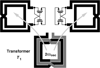
In the presence of mismatches between the core oscillators of Fig. 8.107(b), both the voltage swings at A and B and the mutual coupling between L1 and L2 must exceed a certain minimum to guarantee lock. Note that IA is commutated by M1 and M2 (as in a mixer), experiencing a conversion gain of 2/π.
The above example reveals that techniques that reduce the deviation of the oscillation frequency from the resonance frequency may also lower the flicker noise contribution of the coupling transistors. Specifically, it is possible to introduce additional phase shift in the coupling network by means of passive devices so as to drive Δω in Eqs. (8.194) and (8.195) toward zero. Shown in Fig. 8.109(a) is an example where the degeneration network yields an overall transconductance of
![]()
Figure 8.109 Use of capacitively-degenerated differential pair to create phase shift.
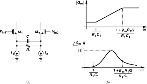
As depicted in Fig. 8.109(b), the phase reaches several tens of degrees between the zero and pole frequencies. However, the degeneration does reduce the coupling factor, requiring larger transistors and bias currents.
In order to avoid the flicker noise of the coupling devices, one can perform the coupling through the bulk of the main transistors. Illustrated in Fig. 8.110 [26], the idea is to apply the differential output of one oscillator to the n-well of the cross-coupled transistors in the other.11 The large resistors R1 and R2 set the bias voltage of the n-wells to VP. Also, C1 and C2 are small enough to create a coupling factor of about 0.25 in conjunction with the n-well-substrate capacitance, CW. Note that this technique still allows two oscillation frequencies.
Figure 8.110 Coupling through n-well of PMOS devices to avoid flicker noise upconversion.
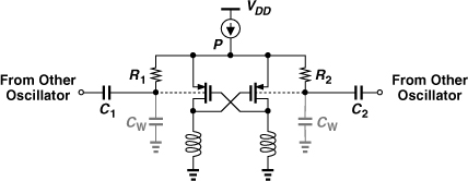
8.12 Appendix A: Simulation of Quadrature Oscillators
In order to examine the tendency of the quadrature oscillator to operate at the frequencies above and below ω0 [Figs. 8.103(b) and 8.104(c)], we simulate the circuit as follows. First, we reconfigure the circuit so that it operates with in-phase coupling and hence at ω0. This simulation provides the exact value of ω0 in the presence of all capacitances.
Next, we apply anti-phase coupling and simulate the circuit, obtaining the exact value of ωosc2 (or ωosc1 if the oscillator prefers the higher mode). Since ω0 − ωosc2 ≈ ωosc1 − ω0, we now have a relatively accurate value for ωosc1.
Last, we inject a sinusoidal current of frequency ωosc1 into the oscillator, Iinj = I0 cos ωosc1t (Fig. 8.111) and allow the circuit to run for a few hundred cycles. If I0 is sufficiently large (e.g., 0.2ISS), the circuit is likely to “lock” to ωosc1. We turn off Iinj after lock is achieved and observe whether the oscillator continues to operate at ωosc1. If it does, then ωosc1 is also a possible solution.
Figure 8.111 Example of injection locking to an external current source.
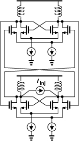
We should also mention that a realistic inductor model is essential to proper simulation of quadrature oscillators. Without the parallel or series resistances that model various loss mechanisms (Chapter 7), the circuit may behave strangely in simulations.
References
[1] B. Razavi, “A 300-GHz Fundamental Oscillator in 65-nm CMOS Technology,” Symposium on VLSI Circuits Dig. Of Tech. Papers, pp. 113–114, June 2010.
[2] R. B. Staszewski et al., “All-Digital PLL and GSM/EDGE Transmitter in 90-nm CMOS,” ISSCC Dig. Tech. Papers, pp. 316–317, Feb. 2005.
[3] D. B. Leeson, “A Simple Model of Feedback Oscillator Noise Spectrum,” Proc. IEEE, vol. 54, pp. 329–330, Feb. 1966.
[4] B. Razavi, “A Study of Phase Noise in CMOS Oscillators,” IEEE Journal of Solid-State Circuits, vol. 31, pp. 331–343, March 1996.
[5] J. Craninckx and M. Steyaert, “Low-Noise Voltage-Controlled Oscillators Using Enhanced LC Tanks,” IEEE Tran. Circuits and Systems, II, vol. 42, pp. 794–804, Dec. 1995.
[6] A. Hajimiri and T. H. Lee, “A General Theory of Phase Noise in Electrical Oscillators,” IEEE J. of Solid-State Circuits, vol. 33, pp. 179–194, Feb. 1998.
[7] J. J. Rael and A. A. Abidi, “Physical Processes of Phase Noise in Differential LC Oscillators,” Proc. CICC, pp. 569–572, May 2000.
[8] J. J. Rael, Phase Noise in Oscillators, PhD Dissertation, University of California, Los Angeles, 2007.
[9] L. W. Couch, Digital and Analog Communication Systems, Fourth Edition, New York: Macmillan Co., 1993.
[10] P. Andreani et al., “A Study of Phase Noise in Colpitts and LC-Tank CMOS Oscillators,” IEEE J. Solid-State Circuits, vol. 40, pp. 1107–1118, May 2005.
[11] P. Andreani and A. Fard, “More on the 1/f Phase Noise Performance of CMOS Differential-Pair LC-Tank Oscillators,” IEEE J. Solid-State Circuits, vol. 41, pp. 2703–2712, Dec. 2006.
[12] C. Samori et al., “Spectrum Folding and Phase Noise in LC Tuned Oscillators,” IEEE Tran. Circuits and Systems, II, vol. 45, pp. 781–791, July 1998.
[13] S. Levantino et al., “AM-to-PM Conversion in Varactor-Tuned Oscillators,” IEEE Tran. Circuits and Systems, II, vol. 49, pp. 509–513, July 2002.
[14] A. Bonfanti et al., “A Varactor Configuration Minimizing the Amplitude-to-Phase Noise Conversion,” IEEE Tran. Circuits and Systems, II, vol. 53, pp. 481–488, March 2006.
[15] B. De Muer et al., “A 2-GHz Low-Phase-Noise Integrated LC-VCO Set with Flicker-Noise Upconversion Minimization,” IEEE J. of Solid-State Circuits, vol. 35, pp. 1034–1038, July 2000.
[16] E. Hegazi, H. Sjoland, and A. A. Abidi, “A Filtering Technique to Lower LC Oscillator Phase Noise,” IEEE J. Solid-State Circuits, vol. 36, pp. 1921–1930, Dec. 2001.
[17] A. Mazzanti and P. Andreani, “Class-C Harmonic CMOS VCOs, with a General Result on Phase Noise,” IEEE J. Solid-State Circuits, vol. 43, no. 12, pp. 2716–2729, Dec. 2008.
[18] T. P. Liu, “A 6.5-GHz Monolithic CMOS Voltage-Controlled Oscillator,” ISSCC Dig. Tech. Papers, pp. 404–405, Feb. 1999.
[19] S. Li, I. Kipnis, and M. Ismail, “A 10-GHz CMOS Quadrature LC-VCO for Multirate Optical Applications,” IEEE J. Solid-State Circuits, vol. 38, pp. 1626–1634, Oct. 2003.
[20] B. Razavi, “Mutual Injection Pulling Between Oscillators,” Proc. CICC, pp. 675–678, Sept. 2006.
[21] P. Andreani et al., “Analysis and Design of a 1.8-GHz CMOS LC Quadrature VCO,” IEEE J. Solid-State Circuits, vol. 37, pp. 1737–1747, Dec. 2002.
[22] L. Romano et al., “Phase Noise and Accuracy in Quadrature Oscillators,” Proc. ISCAS, pp. 161–164, May 2004.
[23] B. Razavi, “Design of Millimeter-Wave CMOS Radios: A Tutorial,” IEEE Trans. Circuits and Systems, I, vol. 56, pp. 4–16, Jan. 2009.
[24] A Mazzanti, F. Svelto, and P. Andreani, “On the Amplitude and Phase Errors of Quadrature LC-Tank CMOS Oscillators,” IEEE J. Solid-State Circuits, vol. 41, pp. 1305–1313, June 2006.
[25] S. Gierkink et al., “A Low-Phase-Noise 5-GHz Quadrature CMOS VCO Using Common-Mode Inductive Coupling,” Proc. ESSCIRC, pp. 539–542, Sept. 2002.
[26] H. R. Kim et al., “A Very Low-Power Quadrature VCO with Back-Gated Coupling,” IEEE J. Solid-State Circuits, vol. 39, pp. 952–955, June 2004.
[27] A. Mazzanti and P. Andreani, “A Time-Variant Analysis of Fundamental 1/f3 Phase Noise in CMOS Parallel LC-Tank Quadrature Oscillator,” IEEE Tran. Circuits and Systems, I, vol. 56, pp. 2173–2181, Oct. 2009.
[28] B. Razavi, “Cognitive Radio Design Challenges and Techniques,” IEEE Journal of Solid-State Circuits, vol. 45, pp. 1542–1553, Aug. 2010.
Problems
8.1. Determine the input admittance of the circuit shown in Fig. 8.4 and find its real part.
8.2. Suppose H(s) in Fig. 8.6 satisfies the following conditions at a frequency ω1: |H(jω1| = 1 but ∠H(jω1) = 170°. Explain what happens.
8.3. Repeat the above problem if |H(jω1| < 1 but ∠H(jω1) = 180°.
8.4. Analyze the oscillator of Fig. 8.15(b) if CGD is not neglected.
8.5. Can any feedback oscillator that employs a lossy resonator be viewed as the one-port system of Fig. 8.13(c)?
8.6. Suppose the inductors in the oscillator of Fig. 8.17(a) exhibit a mismatch of ΔL. Determine the oscillation frequency by calculating the frequency at which the total phase shift around the loop reaches 360°.
8.7. Prove that the series combination of the two tanks in Fig. 8.21(a) can be replaced with one tank as shown in Fig. 8.21(b).
8.8. Compute the tuning range in Example 8.18 if Cb is placed at nodes P and Q in Fig. 8.32(a).
8.9. Why do the PMOS devices in Fig. 8.36 carry a current of ISS?
8.10. For a CS stage loaded by a second-order parallel RLC tank, prove that Rp/(Lω0) = (ω0/2)dφ/dω(= Q).
8.11. Prove that the noise shaping in the system shown in Fig. 8.59 is given by Eq. (8.108).
8.12. Assuming x(t) = A cos ω0t + n(t) = A cos ω0t + nI(t) cos ω0t − nQ(t) sin ω0t, show that the power carried by the AM sidebands is equal to that carried by the PM sidebands and equal to half of the power of n(t).
8.13. Suppose the VCO of Fig. 8.25(a) employs varactors whose capacitance is given by Cvar = C0(1 + α1V + α2V2), where V denotes the gate-source voltage. Assume complete current steering and a low-frequency noise current of In = Im cos ωmt in ISS.
(a) Determine the AM noise resulting from In.
(b) Determine how the average value of the varactor capacitance varies with In.
(c) Compute the phase modulation as a result of the tank resonance frequency modulation.
8.14. Prove that the peak drain voltage swing in Fig. 8.86(b) is no more than roughly VDD− 2(VGS − VTH). To approach this value, the capacitive attenuation must minimize the gate voltage swing.
8.15. Assuming ZT = (L1s)||(C1s)−1||Rp in Fig. 8.100, determine the startup condition.
8.16. For small-signal operation, Eq. (8.194) can be written as
![]()
Now suppose the tail current of the coupling transistors, IT1 contains a flicker noise component, In ![]() IT1. Writing
IT1. Writing ![]() , express Δω as a linear function of In and obtain the corresponding “gain,” KVCO = ∂(Δω)/∂In.
, express Δω as a linear function of In and obtain the corresponding “gain,” KVCO = ∂(Δω)/∂In.
8.17. In the VCO circuit shown in Fig. 8.112, the voltage dependence of each varactor can be expressed as Cvar = C0(1 + α1Vvar), where Vvar denotes the average voltage across the varactor. Use the narrowband FM approximation in this problem. Also, neglect all other capacitances and assume the circuit oscillates at a frequency of ω0 for the given value of Vcont. The dc drop across the inductors is negligible.
(a) Compute the “gain” from ISS to the output frequency, ωout. That is, assume ISS changes by a small value and calculate the voltage change across the varactors and hence the change in the output frequency.
(b) Assume ISS has a noise component that can be expressed as In cos ωnt. Using the result found in (a), determine the frequency and relative magnitude of the resulting output sidebands of the oscillator.
Figure 8.112 VCO with level-shift resistor.
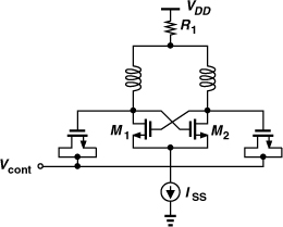
8.18. The circuit shown in Fig. 8.113 is a simplified model of a “dual-mode” oscillator [28]. The voltage-dependent current source models a transistor. The circuit oscillates if Zin goes to infinity for s = jω.
(a) Determine the input impedance Zin.
(b) Set the denominator of Zin to zero for s = jω and obtain the startup condition and the two oscillation frequencies.
Figure 8.113 Simplified model of a dual-mode oscillator.