Chapter 9. Phase-Locked Loops
Most synthesizers employ “phase-locking” to achieve high frequency accuracy. We therefore dedicate this chapter to a study of PLLs. While a detailed treatment of PLLs would consume an entire book, our objective here is to develop enough foundation to allow the analysis and design of RF synthesizers. The outline of the chapter is shown below. The reader is encouraged to review the mathematical model of VCOs described in Chapter 8.
9.1 Basic Concepts
In its simplest form, a PLL is a negative feedback loop consisting of a VCO and a “phase detector” (PD). We therefore first define what a PD is and subsequently construct the loop.
9.1.1 Phase Detector
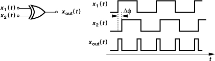
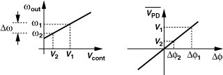
A PD is a circuit that senses two periodic inputs and produces an output whose average value is proportional to the difference between the phases of the inputs. Shown in Fig. 9.1, the input/output characteristic of the PD is ideally a straight line, with a slope called the “gain” and denoted by KPD. For an output voltage quantity, KPD is expressed in V/rad. In practice, the characteristic may not be linear or even monotonic.
Figure 9.1 Phase detector and its input/output characteristic.

How is the phase detector implemented? We seek a circuit whose average output is proportional to the input phase difference. For example, an exclusive-OR (XOR) gate can serve this purpose. As shown in Fig. 9.3, the XOR gate generates pulses whose width is equal to Δφ. In this case, the circuit produces pulses at both the rising edge and the falling edge of the inputs.
Solution:
(a) Assigning a swing of VDD to the output pulses shown in Fig. 9.3, we observe that the output average begins from zero for Δφ = 0 and rises toward VDD as Δφ approaches 180° (because the overlap between the input pulses approaches zero). As Δφ exceeds 180°, the output average falls, reaching zero at Δφ = 360°. Figure 9.4(a) depicts the behavior, revealing a periodic, nonmonotonic characteristic.
Figure 9.4 (a) Input/output characteristic of XOR PD with output swinging between 0 and VDD, (b) input and output waveforms swinging between −V0 and +V0, (c) characteristic corresponding to waveforms of part (b).
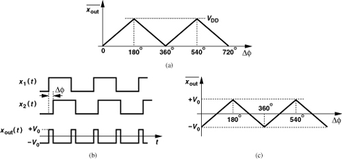
(b) Plotted in Fig. 9.4(b) for a small phase difference, the output exhibits narrow pulses above −V0 and hence an average nearly equal to −V0. As Δφ increases, the output spends more time at +V0, displaying an average of zero for Δφ = 90°. The average continues to increase as Δφ increases and reaches a maximum of +V0 at Δφ = 180°. As shown in Fig. 9.4(c), the average falls thereafter, crossing zero at Δφ = 270° and reaching −V0 at 360°.
9.2 Type-I PLLs
9.2.1 Alignment of a VCO’s Phase
Recall from the mathematical model of VCOs in Chapter 8 that the output phase of a VCO cannot change instantaneously as it requires an ideal impulse on the control voltage. Now, suppose a VCO oscillates at the same frequency as an ideal reference but with a finite phase error (Fig. 9.6). We wish to null this error by adjusting the phase of the VCO. Noting that the control voltage is the only input and that the phase does not change instantaneously, we recognize that we must (1) change the frequency of the VCO, (2) allow the VCO to accumulate phase faster (or more slowly) than the reference so that the phase error vanishes, and (3) change the frequency back to its initial value. As shown in Fig. 9.6, Vcont is stepped at t = t0 and remains at the new value until t = t1, when the phase error goes to zero. Thereafter, the two signals have equal frequencies and a zero phase difference.
Figure 9.6 Alignment of VCO output phase by changing its frequency.

How do we determine the time at which the phase error in Fig. 9.6 reaches zero? A phase detector comparing the VCO phase and the reference phase can serve this purpose, yielding the negative feedback loop shown in Fig. 9.7(a). If the “loop gain” is sufficiently high, the circuit minimizes the input error. Note that the loop only “understands” phase quantities (rather than voltage or current quantities) because the input “subtractor” (the PD) operates with phases.
Figure 9.7 (a) Simple PLL, (b) addition of low-pass filter to remove high-frequency components generated by PD.
The circuit of Fig. 9.7(a) suffers from a critical issue. The phase detector produces repetitive pulses at its output, modulating the VCO frequency and generating large sidebands. We therefore interpose a low-pass filter (called the “loop filter”) between the PD and the VCO so as to suppress these pulses [Fig. 9.7(b)].
9.2.2 Simple PLL
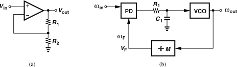
We call the circuit of Fig. 9.7(b) a phase-locked loop and will study its behavior in great detail. But it is helpful to decipher the expressions “phase-locked” or “phase locking.” First, consider the more familiar voltage-domain circuit shown in Fig. 9.8(a). If the open-loop gain of the unity-gain buffer is relatively large, then the output voltage “tracks” the input voltage. Similarly, the PLL of Fig. 9.8(b) ensures that φout(t) tracks φin(t). We say the loop is “locked” if φout(t) − φin(t) is constant (not necessarily zero) with time. We also say the output phase is “locked” to the input phase to emphasize the tracking property.
Figure 9.8 (a) Unity-gain voltage buffer with its output tracking its input, (b) PLL with its output tracking its input.

An important and unique consequence of phase locking is that the input and output frequencies of the PLL are exactly equal. This can be seen by writing
![]()
and hence
![]()
This attribute proves critical to the operation of phase-locked systems, including RF synthesizers.

Can two periodic waveforms have a constant phase difference but different frequencies? If we define the phase difference as the time elapsed between consecutive zero crossings, we observe that this is not possible. That is, if the phases are “locked,” then the frequencies are naturally equal.
9.2.3 Analysis of Simple PLL
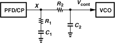
Figure 9.10(a) shows a PLL implementation using an XOR gate and a top-biased LC VCO (Chapter 8). The low-pass filter is realized by means of R1 and C1. If the loop is locked, the input and output frequencies are equal, the PD generates repetitive pulses, the loop filter extracts the average level, and the VCO senses this level so as to operate at the required frequency. Note that the signal of interest changes dimension as we “walk” around the loop: the PD input is a phase quantity, the PD output and the LPF output are voltage quantities, and the VCO output is a phase quantity. By contrast, the unit-gain buffer of Fig. 9.8(a) contains signals in only the voltage and current domains.
Figure 9.10 (a) PLL implementation example, (b) waveforms at different nodes, (c) VCO and PD input/output characteristics showing the system solution.

Following our above study, we may have many questions in regards to PLLs: (1) how does a PLL reach the locked condition? (2) does a PLL always lock? (3) how do we compute the voltages and phases around the loop in the locked condition? (4) how does a PLL respond to a change at its input? In this section, we address some of these questions.
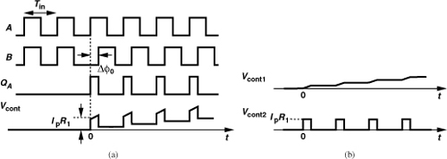
We begin our analysis by examining the signals at various nodes in the circuit of Fig. 9.10(a). Figure 9.10(b) shows the waveforms, assuming the loop is locked. The input and output have equal frequencies but a finite phase difference, Δφ1, and the PD generates pulses whose width is equal to Δφ1. These pulses are low-pass filtered to produce the dc voltage that enables the VCO to operate at a frequency equal to the input frequency, ω1. The residual disturbance on the control line is called the “ripple.” A lower LPF corner frequency further attenuates the ripple, but at the cost of other performance parameters. We return to this point later.
With the VCO and PD characteristics known, it is possible to compute the control voltage of the VCO and the phase error. As illustrated in Fig. 9.10(c), the VCO operates at ω1 if Vcont = V1, and the PD generates a dc value equal to V1 if Δφ = Δφ1. This quantity is called the “static phase error.”
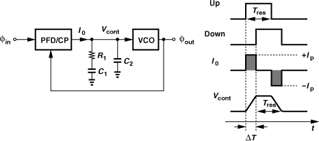
Let us now study, qualitatively, the response of a PLL that is locked for t < t0 and experiences a small, positive frequency step, Δω, at the input at t = t0 (Fig. 9.12). We expect that the loop reaches the final values stipulated in Example 9.6, but we wish to examine the transient behavior. Since the input frequency, ωin, is momentarily greater than the output frequency, ωout, Vin accumulates phase faster, i.e., the phase error begins to grow. Thus, the PD generates increasingly wider pulses, raising the dc level at the output of the LPF and hence the VCO frequency. As the difference between ωout and ωin diminishes, so does the width of the PD output pulses, eventually settling to a value equal to Δω/(KPDKVCO) above its initial value. Also, the control voltage increases by Δω/KVCO.
Figure 9.12 Response of PLL to input frequency step.
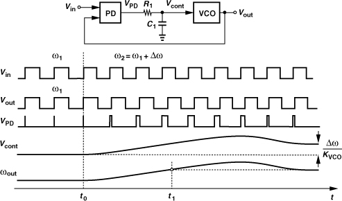
The foregoing study leads to two important points. First, among various nodes in a PLL, the control voltage provides the most straightforward representation of the transient response. By contrast, the VCO or PD outputs do not readily reveal the loop’s settling behavior. Second, the loop locks only after two conditions are satisfied: (1) ωout becomes equal to ωin, and (2) the difference between φin and φout settles to its proper value [1]. For example, the plots in Fig. 9.11 reveal that an input frequency change to ω1 + Δω demands an output frequency change to ω1 + Δω and a phase error change to Δφ2. We also observe from Fig. 9.12 that Vcont becomes equal to its final value at t = t1 (i.e., ωout = ωin at this moment), but the loop continues the transient because the static phase error has not reached its proper value. In other words, both “frequency acquisition” and “phase acquisition” must be completed.

If the input/output phase error of a PLL varies with time, we say the loop is “unlocked,” an undesirable state because the output does not track the input. For example, if at the startup, the VCO frequency is far from the input frequency, the loop may never lock. While the behavior of a PLL in the unlocked state is not important per se, whether and how it acquires lock are both critical issues. In our development of PLLs in this section, we devise a method to guarantee lock.
9.2.4 Loop Dynamics
The transient response of PLLs is generally a nonlinear phenomenon that cannot be formulated easily. Nevertheless, a linear approximation can be used to gain intuition and understand trade-offs in PLL design. We begin our analysis by obtaining the transfer function. Next, we examine the transfer function to predict the time-domain behavior.
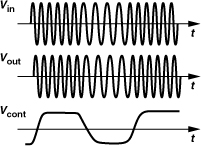
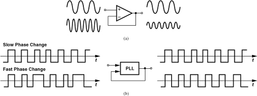
It is instructive to ponder the meaning of the term “transfer function” in a phase-locked system. In the more familiar voltage-domain circuits, such as the unity-gain buffer of Fig. 9.15(a), the transfer function signifies how a sinusoidal input voltage propagates to the output.1 For example, a slow input sinusoid experiences little attenuation, whereas a fast sinusoid emerges with a small voltage amplitude. How do we extend these concepts to the phase domain? The transfer function of a PLL must reveal how a slow or a fast change in the input (excess) phase propagates to the output. Figure 9.15(b) illustrates examples of slow and fast phase change. From Example 9.7, we predict that the PLL’s low-pass behavior “attenuates” the phase excursions if the input phase varies fast. That is, the output phase tracks the input phase closely only for slow phase variations.
Figure 9.15 (a) Response of unity-gain voltage buffer to low or high frequencies, (b) response of PLL to slow or fast input phase changes.
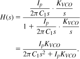
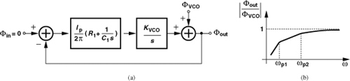
Let us now construct a “phase-domain model” for the PLL. The phase detector simply subtracts the output phase from the input phase and scales the result by a factor of KPD so as to generate an average voltage. As shown in Fig. 9.16, this voltage is applied to the low-pass filter and subsequently to the VCO. Since the phase detector only senses the output phase, the VCO must be modeled as a circuit with a voltage input and a phase output. From the model developed in Chapter 8, the VCO transfer function is expressed as KVCO/s. The open-loop transfer function of the PLL is therefore given by [KPD/(R1C1s + 1)](KVCO/s), yielding an overall closed-loop transfer function of
![]()
Figure 9.16 Phase-domain model of type-I PLL.
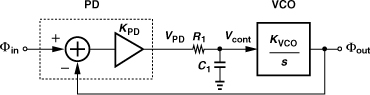
Since the open-loop transfer function contains one pole at the origin (due to the VCO) (i.e., one ideal integrator), this system is called a “type-I PLL.” As expected, for slow input phase variations (s ≈ 0), H(s) ≈ 1, i.e., the output phase tracks the input phase.
The second-order transfer function given by Eq. (9.6) can have an overdamped, critically-damped, or underdamped behavior. To derive the corresponding conditions, we express the denominator in the familiar control theory form, ![]() , where ζ is the “damping factor” and ωn the “natural frequency.” Thus,
, where ζ is the “damping factor” and ωn the “natural frequency.” Thus,
![]()
where

and ωLPF = 1/(R1C1). The damping factor is typically chosen to be ![]() or larger so as to provide a well-behaved (critically damped or overdamped) response.
or larger so as to provide a well-behaved (critically damped or overdamped) response.
Since phase and frequency are related by a linear, time-invariant operation, Eq. (9.6) also applies to frequency quantities. For example, if the input frequency varies slowly, the output frequency tracks it closely.
9.2.5 Frequency Multiplication
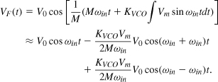
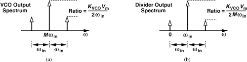
An extremely useful property of PLLs is frequency multiplication, i.e., the generation of an output frequency that is a multiple of the input frequency. How can a PLL “amplify” a frequency? We revisit the more familiar voltage buffer of Fig. 9.8(a) and note that it can provide amplification if its output is divided (attenuated) before returning to the input [Fig. 9.18(a)]. Similarly, the output frequency of a PLL can be divided and then fed back [Fig. 9.18(b)]. The ÷M circuit is a counter that generates one output pulse for every M input pulses (Chapter 10). From another perspective, in the locked condition, ωF = ωin and hence ωout = Mωin. The divide ratio, M, is also called the “modulus.”
Figure 9.18 (a) Voltage amplification, and (b) frequency multiplication.
The PLL of Fig. 9.18(b) can also synthesize frequencies: if the divider modulus changes by 1, the output frequency changes by ωin. This point forms the basis for the frequency synthesizers studied in Chapter 10.
How does the presence of a feedback divider affect the loop dynamics? In analogy with the op amp circuit of Fig. 9.18(a), we surmise that the weaker feedback leads to a slower response and a larger phase error. We study the response in Problem 9.7 and the phase error in the following example.
9.2.6 Drawbacks of Simple PLL
Modern RF synthesizers rarely employ the simple PLL studied here. This is for two reasons. First, Eq. (9.8) imposes a tight relation between the loop stability (ζ) and the corner frequency of the low-pass filter. Recall from Example 9.12 that the ripple on the control line modulates the VCO frequency and must be suppressed by choosing a low value for ωLPF. But, a small ωLPF leads to a less stable loop. We seek a PLL topology that does not exhibit this trade-off.
Second, the simple PLL suffers from a limited “acquisition range,” e.g., if the VCO frequency and the input frequency are very different at the startup, the loop may never “acquire” lock.2 Without delving into the process of lock acquisition, we wish to avoid this issue completely so that the PLL always locks.
While not directly relevant to RF synthesizers, the finite static phase error and its variation with the input frequency [Eq. (9.5)] also prove undesirable in some applications. This error can be driven to zero by means of an infinite loop gain—as explained in the next section.
9.3 Type-II PLLs
We continue our development by first addressing the second issue mentioned above, namely, the problem of limited acquisition range. While beyond the scope of this book, this limitation arises because phase detectors produce little information if they sense unequal frequencies at their inputs. We therefore postulate that the acquisition range can be widened if a frequency detector is added to the loop. Of course, we note from Example 9.5 that an FD by itself does not suffice and the loop must eventually lock the phases. Thus, it is desirable to seek a circuit that operates as an FD if its input frequencies are not equal and as a PD if they are. Such a circuit is called a “phase/frequency detector” (PFD).
9.3.1 Phase/Frequency Detectors
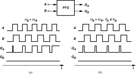
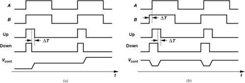
Figure 9.20 conceptually shows the operation of a PFD. The circuit produces two outputs, QA and QB, and operates based on the following principles: (1) a rising edge on A yields a rising edge on QA (if QA is low), and (2) a rising edge on B resets QA (if QA is high). The circuit is symmetric with respect to A and B (and QA and QB). We observe from Fig. 9.20(a) that, if ωA > ωB, then QA produces pulses while QB remains at zero. Conversely, if ωB > ωA, then positive pulses appear at QB and QA = 0. On the other hand, as depicted in Fig. 9.20(b), if ωA = ωB, the circuit generates pulses at either QA or QB with a width equal to the phase difference between A and B. Thus, the average value of QA − QB represents the frequency or phase difference.
Figure 9.20 Response of a PFD to inputs with unequal (a) frequencies, or (b) phases.
To arrive at a circuit implementation of the above idea, we surmise that at least three logical states are necessary: QA = QB = 0; QA = 0, QB = 1; and QA = 1, QB = 0. Also, to avoid dependence of the output upon the duty cycle of the inputs, the circuit should be realized as an edge-triggered sequential machine. Figure 9.21 shows a state diagram summarizing the operation. If the PFD is in state 0, then a transition on A takes it to state I, where QA = 1, QB = 0. The circuit remains in this state until a transition occurs on B, upon which the PFD returns to state 0. The switching sequence between states 0 and II is similar.
Figure 9.21 State diagram showing desired operation of PFD.
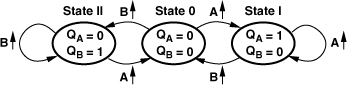
Figure 9.22 illustrates a logical implementation of the above state machine. The circuit consists of two edge-triggered, resettable D flipflops with their D inputs tied to logical ONE. Signals A and B act as clock inputs of DFFA and DFFB, respectively, and the AND gate resets the flipflops if QA = QB = 1. We note that a transition on A forces QA to be equal to D input, i.e., a logical ONE. Subsequent transitions on A have no effect. When B goes high, so does QB, activating the reset of the flipflops. Thus, QA and QB are simultaneously high for a duration given by the total delay through the AND gate and the reset path of the flipflops. The reader can show that, if A and B are exactly in-phase, both QA and QB exhibit these narrow “reset pulses.”
Figure 9.22 PFD implementation.
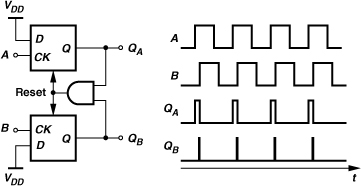
What is the effect of reset pulses on QB in Fig. 9.22? Since only the average value of QA − QB is of interest, these pulses do not interfere with the operation. However, as explained in Section 9.4, the reset pulses introduce a number of errors that tend to increase the ripple on the control voltage.
Each resettable D-flipflop in Fig. 9.22 can be implemented as shown in Fig. 9.23. (Note that no D input is available.) This circuit suffers from a limited speed—a minor issue because in frequency-multiplying PLLs, ωin is typically much lower than ωout. For example, in a GSM system, one may choose ωin = 2π × (200 kHz) and ωout = 2π × (900 MHz). By analyzing the propagation of the reset command in Figs. 9.22 and 9.23, the reader can show that the width of the narrow reset pulses on QA and QB is equal to three gate delays plus the delay of the AND gate. If the AND gate consists of a NAND gate and an inverter, the pulse width reaches five gate delays. We hereafter assume the reset pulses are five gate delays wide for a zero input phase difference.
Figure 9.23 Logical implementation of resettable D flipflop.

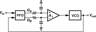
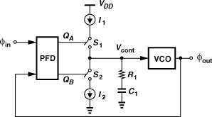
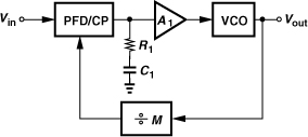
The use of a PFD in a phase-locked loop resolves the issue of the limited acquisition range. Shown in Fig. 9.24 is a conceptual realization employing a PFD. The dc content of QA − QB is extracted by the low-pass filters and amplifier A1. At the beginning of a transient, the PFD acts as a frequency detector, pushing the VCO frequency toward the input frequency. After the two are sufficiently close, the PFD operates as a phase detector, bringing the loop into phase lock. Note that the polarity of feedback is important here [but not in the simple PLL (Example 9.11)].
Figure 9.24 Use of PFD in a type-I PLL.
We must next address the trade-off between the damping factor and the corner frequency of the loop filter [Eq. (9.8)]. This is accomplished by introducing a “charge pump” (CP) in the loop.
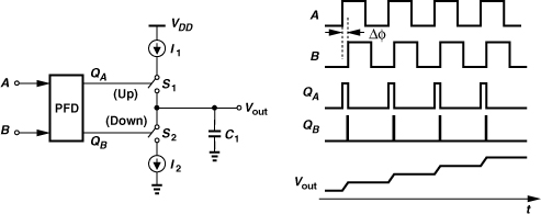
9.3.2 Charge Pumps
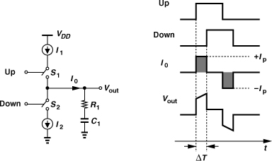
A charge pump sinks or sources current for a limited period of time. Depicted in Fig. 9.25 is an example, where switches S1 and S2 are controlled by the inputs “Up” and “Down,” respectively. A pulse of width ΔT on Up turns S1 on for ΔT seconds, allowing I1 to charge C1. Consequently, Vout goes up by an amount equal to ΔT · I1/C1. Similarly, a pulse on Down yields a drop in Vout. Nominally, I1 = I2 = Ip. Thus, if Up and Down are asserted simultaneously, I1 simply flows through S1 and S2 to I2, creating no change in Vout.

Let us precede the circuit of Fig. 9.25 with a PFD (Fig. 9.26). We note that if, for example, A leads B, then QA produces pulses and Vout continues to rise. A key point here is that an arbitrarily small (constant) phase difference between A and B still turns one switch on—albeit briefly—thereby charging or discharging C1 and driving Vout toward +∞ or −∞—albeit slowly. In other words, the circuit of Fig. 9.26 exhibits an infinite gain, where the gain is defined as the final value of Vout divided by the input phase difference. From another perspective, the PFD/CP/C1 cascade produces a ramp-like output in response to a constant phase difference, displaying the behavior of an integrator.
Figure 9.26 Operation of PFD/CP cascade.
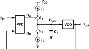
9.3.3 Charge-Pump PLLs
We now construct a PLL using the circuit of Fig. 9.26. Illustrated in Fig. 9.27, such a loop ideally forces the input phase error to zero because, as mentioned in the previous section, a finite error would lead to an unbounded value for Vcont. To quantify the behavior of this arrangement, we wish to derive the transfer function from φin to φout. Let us first study the transfer function of the PFD/CP/C1 cascade.
Figure 9.27 First attempt at constructing a charge-pump PLL.
How do we compute this transfer function? We can apply a (phase) step at the input, derive the time-domain output, differentiate it, and compute its Laplace transform [2]. A phase step simply means a displacement of the zero crossings. As shown in Fig. 9.28, a phase step of Δφ0 at one of the inputs repetitively turns S1 or S2 on, monotonically changing the output voltage.
Figure 9.28 Derivation of the phase step response of PFD/CP/capacitor cascade.
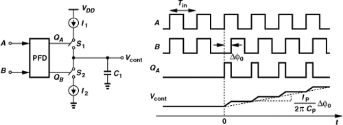
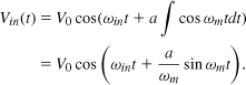
This behavior is similar to that of an integrator. Unfortunately, however, this system is nonlinear: if Δφ0 is doubled, not every point on the “charge-and-hold” output waveform, Vout, is doubled (why?). Fortunately, we can approximate this waveform by a ramp—as if the charge pump continuously injected current into C1 (Example 9.14). We call this a “continuous-time (CT) approximation.” The change in Vcont in every period is equal to
![]()
where [Δφ0/(2π)]Tin denotes the phase difference in seconds and Ip = I1 = I2. The slope of the ramp is given by ΔVcont/Tin and hence
![]()
Differentiating Eq. (9.13) with respect to time, normalizing to Δφ0, and taking the Laplace transform, we have
![]()
As predicted earlier, the PFD/CP/C1 cascade operates as an integrator.
Solution:
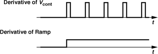
Figure 9.29 Comparison of the derivatives of the actual phase step response of PFD/CP/capacitor cascade and a ramp.
From Eq. (9.14), the closed-loop transfer function of the PLL shown in Fig. 9.27 can be expressed as
This arrangement is called a type-II PLL because its open-loop transfer function contains two poles at the origin (i.e., two ideal integrators).
Equation (9.16) reveals two poles on the jω axis, indicating an oscillatory system. From Example 8.5 for two ideal (lossless) integrators in a loop, we note that the instability is to be expected. We thus postulate that if one of the integrators becomes lossy, the system can be stabilized. This can be accomplished by inserting a resistor in series with C1 (Fig. 9.30). The resulting circuit is called a “charge-pump PLL” (CPPLL).
We repeat the analysis illustrated in Fig. 9.28(a) to obtain the new transfer function. As shown in Fig. 9.31, when S1 or S2 turns on, Vcont jumps by an amount equal to IpR1 and subsequently rises or falls linearly with time. When the switch turns off, Vcont jumps in the opposite direction, resting at a voltage that is (Ip/C1)[Δφ0/(2π)]Tin volts higher than its value before the switch turned on. The resulting waveform can be viewed as the sum of the original charge-and-hold waveform and a sequence of pulses [Fig. 9.28(b)]. The area under each pulse is approximately equal to (IpR1)[Δφ0/(2π)]Tin. As in Example 9.15, if the time scale of interest is much longer than Tin, we can approximate the pulse sequence by a step of height (IpR1)[Δφ0/(2π)]. It follows that
![]()
Figure 9.31 (a) Phase step response of PFD/CP/LPF, (b) decomposition of output waveform into two.
The transfer function of the PFD/CP/filter cascade is therefore given by
![]()
Equation (9.18) allows us to express the closed-loop transfer function of the PLL shown in Fig. 9.30 as

As with the type-I PLL in Section 9.2, we write the denominator as ![]() and obtain
and obtain
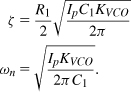
Interestingly, as C1 increases (so as to reduce the ripple on the control voltage), so does ζ—a trend opposite of that observed in type-I PLLs. We have thus removed the trade-off between stability and ripple amplitude. The closed-loop poles are given by
![]()
Equation (9.19) also reveals a closed-loop zero at −ωn/(2ζ).
The transfer function expressed by Eq. (9.18) offers another perspective on stabilization (frequency compensation) of a two-integrator loop. Writing (9.18) as
![]()
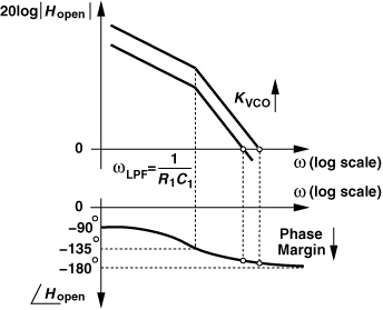
we can say that a real left-half-plane zero, ωz = −1/(R1C1), has been added to the open-loop transfer function, thereby stabilizing the PLL. This point can be better understood by examining the Bode plots of the loop before and after compensation. As shown in Fig. 9.32, with two ideal integrators, the system has no phase margin, whereas with the zero, both the magnitude and the phase profiles are bent upward, increasing the phase margin.
Figure 9.32 Bode plots of open-loop charge-pump PLL with and without a zero.
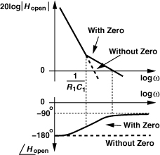
The behavior illustrated in Fig. 9.32 also explains the dependence of ζ upon KVCO [Eq. (9.20)]. As KVCO decreases, the magnitude plot is shifted down while the phase plot remains unchanged. Thus, the unity-gain frequency moves closer to the −180° region, degrading the phase margin. This stands in contrast to the type-I PLL’s behavior in Example 9.10.
Suppose during the lock transient, the phase difference is not zero at some point in time. Then, a current of Ip flows through R1, producing a voltage drop of IpR1. In Problem 9.10, we estimate this drop to be 1.6πVDD. (Of course, the CP cannot provide such a large swing.) The key point here is that the control voltage can experience a large jump. We return to this point in Section 9.3.7 and observe that this jump appears even in the locked state, creating significant ripple.
9.3.4 Transient Response
The closed-loop transfer function of the PLL, as expressed by Eq. (9.19), can be used to predict the transient response.
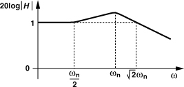
Solution:
The closed loop contains two real coincident poles at −ωn and a zero at −ωn/2. Depicted in Fig. 9.33 |H| begins to rise from unity at ω = ωn/2, reaches a peak at ω = ωn, returns to unity at ![]() , and continues to fall at a slope of −20 dB/dec thereafter.
, and continues to fall at a slope of −20 dB/dec thereafter.
Figure 9.33 Closed-loop PLL frequency response for two coincident closed-loop poles.
The inverse Laplace transform of Eq. (9.19) yields the output frequency, Δωout, as a function of time for a frequency step at the input, Δωin:
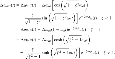
Since the response decays exponentially, we may call 1/(ζ ωn) the “time constant” of the loop, but, as explained below, that is not an accurate statement. Note that (9.24) can be simplified if we assume ![]() (i.e., ζ = sin ψ):
(i.e., ζ = sin ψ):
![]()
From (9.20) and (9.21), the time constant of the loop is expressed as
![]()
This quantity (or its inverse) serves as a measure of the settling speed of the loop if ζ is in the vicinity of unity.
What happens as ζ well exceeds unity? If ζ2 ![]() 1, then
1, then ![]() , and Eq. (9.22) reduces to
, and Eq. (9.22) reduces to
![]()
![]()
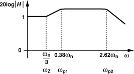
Note that ωp1/ωp2 ≈ 4ζ2 ![]() 1. Does this mean ωp2 becomes a dominant pole? No, interestingly, the zero is also located at −ωn/(2ζ), cancelling the effect of ωp2. Thus, for large ζ2, the loop approaches a one-pole system having a time constant of 1/|ωp1| = 1/(2ζωn). Figure 9.34 plots |H| for ζ = 1.5, indicating that even this value of ζ leads to an approximately one-pole response because ωz and ωp1 are relatively close.
1. Does this mean ωp2 becomes a dominant pole? No, interestingly, the zero is also located at −ωn/(2ζ), cancelling the effect of ωp2. Thus, for large ζ2, the loop approaches a one-pole system having a time constant of 1/|ωp1| = 1/(2ζωn). Figure 9.34 plots |H| for ζ = 1.5, indicating that even this value of ζ leads to an approximately one-pole response because ωz and ωp1 are relatively close.
Figure 9.34 Closed-loop PLL frequency response for ζ = 1.5.
A student has encountered an inconsistency in our derivations. We concluded above that the loop time constant is approximately equal to 1/(2ζωn) for ζ2 ![]() 1, but (9.24)-(9.26) evidently imply a time constant of 1/(ζωn). Explain the cause of this inconsistency.
1, but (9.24)-(9.26) evidently imply a time constant of 1/(ζωn). Explain the cause of this inconsistency.
Solution:
For ζ2 ![]() 1, we have
1, we have ![]() . Since cosh x − sinh x = e−x, we rewrite Eq. (9.26) as
. Since cosh x − sinh x = e−x, we rewrite Eq. (9.26) as
![]()
9.3.5 Limitations of Continuous-Time Approximation
Charge-pump PLLs are inherently discrete-time (DT) systems because the charge pump turns off for part of the period and breaks the loop. In the derivation of the CPPLL transfer function, we have made two continuous-time approximations: the charge-and-hold waveform in Fig. 9.28 is represented by a ramp, and the series of pulses in Fig. 9.31(b) is modeled by a step. These approximations hold only if the time “granularities” inherent in the original waveforms are very small with respect to the time scales of interest. To better understand this point, let us consider the inverse problem, namely, the approximation of a CT waveform by a DT counterpart. As illustrated in Fig. 9.35, the approximation holds well if the CT waveform changes little from one clock cycle to the next, but loses its accuracy if the CT waveform experiences fast changes.
Figure 9.35 (a) Accurate and (b) poor discrete-time approximations of continuous-time waveforms.
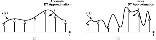
These observations reveal that CPPLLs obey the transfer function of Eq. (9.19) only if their internal states (the control voltage and the VCO phase) do not change rapidly from one input cycle to the next. This occurs if the loop time constant is much longer than the input period. Indeed, this point plays an important role in the design procedure of PLLs (Section 9.7). Discrete-time analyses of CPPLLs can be found in [3], but in practice, loops that are not sufficiently slow exhibit an underdamped behavior or may simply not lock. The CT approximation therefore proves adequate in most practical cases.
9.3.6 Frequency-Multiplying CPPLL
As explained in Section 9.2.5 and illustrated in Fig. 9.18(b), a PLL containing a divider of modulus M in its feedback path multiplies the input frequency by a factor of M. We wish to formulate the dynamics of a type-II frequency-multiplying PLL. We simply consider the product of (9.23) and KVCO/s as the forward transfer function and 1/M as the feedback factor, arriving at

The denominator is similar to that of Eq. (9.19), except that KVCO is divided by M. Thus, (9.20) and (9.21) can be respectively modified to
![]()
![]()
As can be seen in Fig. 9.32, the division of KVCO by M makes the loop less stable (why?), requiring that Ip and/or C1 be larger. We can rewrite (9.32) as
![]()
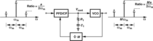
It is important to recognize that the above example applies to only slow phase or frequency modulation at the PLL input such that the output tracks the variation faithfully. For faster modulations, the output phase is an attenuated version of the input and subjected to Eq. (9.32).
9.3.7 Higher-Order Loops
The loop filter consisting of R1 and C1 in Fig. 9.30 proves inadequate because, even in the locked condition, it does not suppress the ripple sufficiently. For example, suppose, in the locked condition, the Up and Down pulses arrive every Tin seconds with a small skew due to propagation mismatches within the PFD (Fig. 9.37). Consequently, one switch turns on earlier than the other, allowing its corresponding current source to flow through R1 and generate an instantaneous change of IpR1 in the control voltage. On the falling edge of the Up and Down pulses, the reverse happens. The ripple thus consists of positive and negative pulses of amplitude IpR1 occurring every Tin seconds. Since IpR1 is quite large (even higher than the supply voltage!),3 additional means of reducing the ripple become necessary.
Figure 9.37 Effect of skew between Up and Down pulses.
A common approach to lowering the ripple is to tie a capacitor directly from the control line to ground. Illustrated in Fig. 9.38, the idea is to provide a low-impedance path for the unwanted charge pump output. That is, a current pulse of width ΔT produced by the CP initially flows through C2, leading to a change of (Ip/C2)ΔT in Vcont. (Since typically R1C2 ![]() ΔT, the voltage change can be approximated by a ramp.) After the CP turns off, C2 begins to share its charge with C1 through R1, causing an exponential decay in Vcont with a time constant of R1Ceq, where Ceq = C1C2/(C1 + C2). Of course, it is hoped that C2 can be large enough to yield a small ripple.
ΔT, the voltage change can be approximated by a ramp.) After the CP turns off, C2 begins to share its charge with C1 through R1, causing an exponential decay in Vcont with a time constant of R1Ceq, where Ceq = C1C2/(C1 + C2). Of course, it is hoped that C2 can be large enough to yield a small ripple.
Figure 9.38 Addition of second capacitor to loop filter.

How large can C2 be? The current-to-voltage conversion impedance provided by the loop filter has changed from R1 + (C1s)−1 to [R1 + (C1s)−1]||(C2s)−1, presenting an additional pole at (R1Ceq)−1 and degrading the loop stability. We must therefore compute the phase margin before and after addition of C2. As shown in Appendix I,
![]()
where ζ is chosen equal to ![]() to maximize PM. For example, if C2 = 0.2C1, then (R1Ceq)−1 = 6ωz, ζ ≈ 0.783, and the phase margin falls from 76° to 46°. Simulations of PLLs indicate that this estimate is somewhat pessimistic and C2 ≤ 0.2C1 is a reasonable choice in most cases. We therefore choose ζ = 0.8-1 and C2 ≈ 0.2C1 in typical designs.4
to maximize PM. For example, if C2 = 0.2C1, then (R1Ceq)−1 = 6ωz, ζ ≈ 0.783, and the phase margin falls from 76° to 46°. Simulations of PLLs indicate that this estimate is somewhat pessimistic and C2 ≤ 0.2C1 is a reasonable choice in most cases. We therefore choose ζ = 0.8-1 and C2 ≈ 0.2C1 in typical designs.4
Unfortunately, with C2 present, R1 cannot be arbitrarily large. In fact, if R1 is so large that the series combination of R1 and C1 is overwhelmed by C2, then the PLL reduces to the system shown in Fig. 9.27 and characterized by Eq. (9.16). An upper bound derived for R1 in Appendix I is as follows:
![]()

Another loop filter that can reduce the ripple is shown in Fig. 9.40. Here, the ripple at node X may be large, but it is suppressed as it travels through the low-pass filter consisting of R2 and C2. If |R2 + (C2s)−1| ![]() |R1 + (C1s)−1| at the frequencies of interest, then the additional pole is given by (R2C2)−1. Following the analysis in Appendix I, the reader can prove that
|R1 + (C1s)−1| at the frequencies of interest, then the additional pole is given by (R2C2)−1. Following the analysis in Appendix I, the reader can prove that
![]()
Figure 9.40 Alternative second-order loop filter.
Thus, (R2C2)−1 must remain 5 to 10 times higher than ωz so as to yield a reasonable phase margin.
9.4 PFD/CP Nonidealities
Our study of PLLs in the previous sections has provided a detailed understanding of their basic operation but has neglected various imperfections. In this section, we analyze the effect of nonidealities in the PFD/CP cascade. We also present circuit techniques that combat some of these effects.
9.4.1 Up and Down Skew and Width Mismatch
The Up and Down pulses produced by the PFD may arrive at different times. As explained in Section 9.3.7 and illustrated in Fig. 9.37, an arrival time mismatch of ΔT translates to two current pulses of width ΔT, height Ip, and opposite polarities that are injected by the charge pump at each phase comparison instant. Owing to the short time scales associated with these pulses, only C2 in Fig. 9.38 acts as a storage element, producing a pulse on the control line (Fig. 9.41). The width of the pulse is equal to the width of the reset pulses, Tres (about 5 gate delays for the PFD implementation of Figs. 9.22 and 9.23), plus ΔT. The height of the pulse is equal to ΔTIp/C2.
Figure 9.41 Effect of Up and Down skew on Vcont for a second-order filter.
Solution:
The area under each pulse is approximately given by (ΔTIp/C2)Tres if Tres ![]() 2ΔT. The Fourier transform of the sequence therefore contains impulses at the multiples of the input frequency, fin = 1/Tin, with an amplitude of (ΔTIp/C2)Tres/Tin (Fig. 9.42). The two impulses at ±1/Tin correspond to a sinusoid having a peak amplitude of 2ΔTIpC2Tres/Tin. If the narrowband FM approximation holds, we conclude that the relative magnitude of the sidebands at fc ± fin at the VCO output is given by
2ΔT. The Fourier transform of the sequence therefore contains impulses at the multiples of the input frequency, fin = 1/Tin, with an amplitude of (ΔTIp/C2)Tres/Tin (Fig. 9.42). The two impulses at ±1/Tin correspond to a sinusoid having a peak amplitude of 2ΔTIpC2Tres/Tin. If the narrowband FM approximation holds, we conclude that the relative magnitude of the sidebands at fc ± fin at the VCO output is given by
![]()
Figure 9.42 Spectrum of ripple on control voltage.

The reader may wonder how the Up and Down pulses may arrive at different times. In addition to random propagation time mismatches with the PFD, the interface between the PFD and the charge pump may also introduce a systematic skew. For example, consider the arrangement shown in Fig. 9.43(a), where the charge pump is implemented by M1-M4. Since S1 is realized by a PMOS device, the corresponding PFD output, QA, must be inverted so that M1 is on when QA is high. The delay of the inverter thus creates a skew between the Up and Down pulses. To alleviate this issue, a transmission gate can be inserted in the Down pulse path so as to replicate the delay of the inverter [Fig. 9.43(b)].5
Figure 9.43 (a) Skew between Up and Down pulses as a result of additional inverter, (b) skew compensation by a pass gate, (c) current waveforms showing effect of skew.
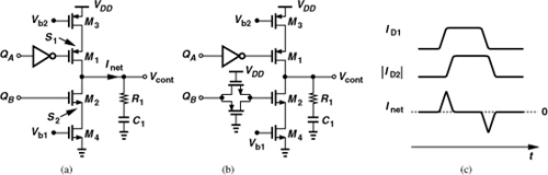
Does perfect alignment of Up and Down pulses in Fig. 9.43(b) suffice? Not necessarily; the currents produced by the PMOS and NMOS sections of the charge pump may still suffer from skews. This is because the time instants at which M1 and M2 turn on and off may not be aligned. In other words, the quantity of interest is in fact the skew between the Up and Down current waveforms, ID1 and ID2 in Fig. 9.43(c), respectively, or, ultimately, the net current injected into the loop filter, Inet = ID1 − ID2. In the design of the PFD/CP combination, Inet must be minimized in amplitude and in duration.
Solution:
Figure 9.44 Effect of Up and Down width mismatch: (a) initial response, (b) steady-state response.
9.4.2 Voltage Compliance
Recall from Chapter 8 that we wish to maximize the tuning range of VCOs while maintaining a moderate value for KVCO. It is therefore desirable to design the charge pump so that it produces minimum and maximum voltages as close to the supply rails as possible. In the simple charge pump of Fig. 9.43(b), each current source requires a minimum drain-source voltage and each switch sustains a voltage drop. We say the output compliance is equal to VDD minus two overdrive voltages and two switch drops. To maximize the output compliance, wide devices must be employed, but at the cost of exacerbating some of the issues described below.
9.4.3 Charge Injection and Clock Feedthrough
We now turn our attention to the imperfections introduced by the charge pump. We assume the simple CP implementation of Fig. 9.43(b) for now. The switching transistors, M1 and M2, carry a certain amount of mobile charge in their inversion layers when they are on. This charge is expressed as
![]()
As the switches turn on, they absorb this charge and as they turn off, they dispel this charge, in both cases through their source and drain terminals. Since M1 and M2 generally have different dimensions and overdrive voltages, they do not cancel each other’s charge absorption or injection, thereby disturbing the control voltage at both turn-on and turn-off points [Fig. 9.45(a)]. We hereafter refer to this effect as charge injection and consider it when switches turn off, bearing in mind that charge absorption plays a similar role.
Figure 9.45 (a) Channel charge injection, and (b) clock feedthrough in a charge pump.
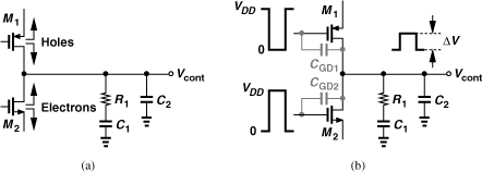
Another effect relates to the gate-drain overlap capacitance of the switches. As shown in Fig. 9.45(b), the Up and Down pulses couple through CGD1 and CGD2, respectively, and reach Vcont. Since R1C1 is quite long, only C2 attenuates this “clock feedthrough” initially
![]()
After the charge pump turns off, charge sharing between C2 and C1 reduces this voltage to
![]()
A number of techniques can reduce the effect of charge injection and clock feedthrough. Depicted in Fig. 9.46(a), one approach places the switches near the supply rails [4] so that the feedthrough is somewhat attenuated by the total capacitance seen from X and Y to ground before disturbing the source voltage of M3 and M4. Charge injection, however, persists because M3 and M4 must still dispel their charge when they turn off. This approach is called “source switching” because the switches are tied to the sources of M3 and M4.
Figure 9.46 Improved charge pumps: (a) source-switched CP, (b) use of dummy switches, (c) use of differential pairs.
Another method incorporates “dummy” switches to suppress both effects [5]. Illustrated in Fig. 9.46(b), the idea is to add transistors configured as capacitors and driven by the complements of Up and Down pulses. The reader can prove that, if W5 = 0.5W1 and W6 = 0.5W2, then the clock feedthrough of each switch is cancelled. The charge injection is also cancelled if, additionally, the charge of each switch splits equally between its source and drain terminals. Since this condition is difficult to guarantee, charge injection may be only partially removed.
Figure 9.46(c) shows another arrangement, where the Up and Down currents are created by differential pairs. If Vb1 and Vb2 provide a low impedance at the gates of M1 and M2, respectively, then ![]() and
and ![]() find no feedthrough path to the output. However, the charge injection mismatch between M1 and M2 remains uncorrected.
find no feedthrough path to the output. However, the charge injection mismatch between M1 and M2 remains uncorrected.
9.4.4 Random Mismatch between Up and Down Currents
The two current sources in a charge pump inevitably suffer from random mismatches. Figure 9.47(a) shows an example, where IREF is copied onto M4 and M6 and ID6 onto M3. We note that mismatches between M4 and M6 and between M3 and M5 manifest themselves in the Up and Down currents. How does the PLL react to this mismatch? If, as depicted in Fig. 9.47(b), the Up and Down pulses remain aligned, then a net positive (or negative) current is injected into the loop filter, yielding an unbounded control voltage (in a manner similar to Example 9.22). The loop must therefore develop a phase offset such that the smaller current lasts longer [Fig. 9.47(c)]. For a mismatch of ΔI, the net current is zero if
![]()
where Ip denotes the mean current. Thus,
![]()
Figure 9.47 (a) Simple CP realization, (b) initial response to Up and Down current mismatch, (c) steady-state response to Up and Down current mismatch.
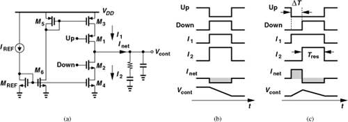
The ripple amplitude is equal to ΔT · Ip/C2 = TresΔI/C2.
How does the ripple due to Up and Down skew compare with that due to current mismatch? As derived earlier, the former has an amplitude equal to ΔT · Ip/C2. Thus, one is proportional to the skew times the entire charge pump current whereas the other is proportional to the reset pulsewidth times the current mismatch. The two may thus be comparable.
The random mismatch between the Up and Down currents can be reduced by enlarging the current-source transistors. Recall from analog design that as the device area increases, mismatches experience greater spatial averaging. For example, doubling the area of a transistor—equivalent to placing two transistors in parallel—reduces the threshold voltage mismatch by a factor of ![]() . However, larger transistors suffer from a greater amount of charge injection and clock feedthrough.
. However, larger transistors suffer from a greater amount of charge injection and clock feedthrough.
9.4.5 Channel-Length Modulation
The Up and Down currents also incur mismatch due to channel-length modulation of the current sources; i.e., different output voltages inevitably lead to opposite changes in the drain-source voltages of the current sources, thereby creating a larger mismatch.
In order to quantify the effect of channel-length modulation, we test the charge pump as shown in Fig. 9.48(a). Both switches are on and the output voltage is swept across the compliance range. In the ideal case, IX = 0 for the entire range, but in reality, IX varies as shown in Fig. 9.48(b) because the PMOS or NMOS source carries a larger current than the other. The maximum departure of IX from zero, Imax, divided by the nominal value of Ip quantifies the effect of channel-length modulation. With short-channel devices, this ratio may reach 30-48%.
Figure 9.48 (a) Charge pump configured to measure effect of channel-length modulation, (b) behavior of IX.

While the phase offset or its variation is not critical in RF synthesis, the resulting ripple is. That is, channel-length modulation must be small enough to produce a tolerable ripple amplitude ( = TresΔI/C2). Longer transistors can alleviate this effect, but in practice it may be difficult to achieve sufficiently small ΔI. For this reason, a number of circuit techniques have been devised to deal with channel-length modulation.
9.4.6 Circuit Techniques
It is possible to raise the output impedance of the current sources through the use of “regulated cascodes” [6]. Figure 9.50(a) illustrates such a structure, where an “auxiliary amplifier,” A0, senses VP and adjusts the gate voltage of M1 so as to maintain VP close to Vb and hence the current through RS, IX, relatively constant. As a result, the output impedance rises. The reader can use a small-signal model to prove that
![]()
Figure 9.50 (a) Circuit using an amplifier to raise the output impedance, (b) use of technique in (a) in a charge pump.
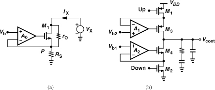
This technique is attractive because it raises the output impedance without consuming additional voltage headroom.
Figure 9.50(b) shows a charge pump employing regulated cascodes. Note that the switches are placed in series with the sources of M3 and M4. If the gain of the auxiliary amplifiers is sufficiently large, the mismatch between the Up and Down currents remains small even if M3 and M4 enter the triode region by a small amount.
The principal drawback of this approach stems from the finite response of the auxiliary amplifiers. When M1 and M2 turn off, the feedback loops around M3 and M4 are broken, allowing the outputs of A1 and A2 to approach the supply rails. In the next phase comparison instant, these outputs must return and settle to their proper values—a transient substantially longer than the width of the Up and Down pulses (≈ five gate delays). In other words, A1 and A2 may simply not have enough time to settle and boost the output impedance according to Eq. (9.49).
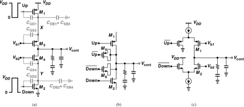
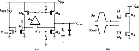
Figure 9.51 depicts another technique [7]. Here, M1-M4 constitute the main charge pump and M5-M8 a replica branch. Note that the bias current of MREF is copied onto M6 and M4, and additional transistors M9 and M8 imitate the role of M2 (when it is on). Neglecting random mismatches and assuming a ratio of unity between the CP branch and its replica, we show that the Up current is forced to become equal to the Down current even in the presence of channel-length modulation. We first recognize that, in the locked state, the loop filter serves as a heavy “reservoir,” keeping Vcont relatively constant. Thus, the servo amplifier, A0, adjusts the gate voltage of M5 so as to bring VX close to Vcont. This in turn means that ID6 ≈ ID4 (because VD6 ≈ VD4) and ID5 ≈ ID3 even if the transistors suffer from heavy channel-length modulation. Moreover, since |ID5| = |ID6|, we have |ID3| = ID4, i.e., the Up and Down currents are equal. The circuit can therefore tolerate a wide output voltage range so long as the open-loop gain of A0 is sufficiently large to guarantee VX ≈ Vcont.
Figure 9.51 Use of a servo loop to suppress the effect of channel-length modulation.

A key advantage of this topology over the charge pump in Fig. 9.50(b) is that A0 need not provide a fast response. This is because, when M1 and M2 turn off, the feedback loop consisting of A0 and M5 remains intact, thus experiencing a negligible transient.
The performance of the circuit is still limited by random mismatches between the NMOS current sources and between the PMOS current sources. Also, the op amp must operate properly with a nearly rail-to-rail input common-mode range because Vcont must come as close to the rails as possible.
Figure 9.52(a) shows another example using a servo amplifier [8]. In a manner similar to Fig. 9.51, A0 forces VX close to Vcont such that ID5 ≈ ID4 and ID6 ≈ ID3 (in the absence of random mismatches). Consequently, |ID3| ≈ ID4. This circuit, however, controls the Up and Down currents through the gates of M3 and M4, respectively, thereby saving the voltage headroom associated with M1 and M2 in Fig. 9.51. This approach is called “gate switching.”
Figure 9.52 (a) Use of a servo loop to suppress the effect of channel-length modulation in a gate-switched CP, (b) effect of process variations on Up and Down skew.
The gate switching operation nonetheless exacerbates the problem of Up and Down arrival mismatch. To understand this issue, let us consider the realization shown in Fig. 9.52(b), where the Up and Down pulses have a finite risetime and falltime. We observe that M1 turns on or off as the Up pulse reaches VDD − |VGS3| − |VTH1|, whereas M2 turns on or off as the Down pulse crosses VGS4 + VTH2. Since both of these values vary with process and temperature, it is difficult to ensure that the Up and Down currents arrive simultaneously. Also, op amp A0 must operate with a wide input voltage range.
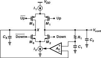
Depicted in Fig. 9.53 is another example that cancels both random and deterministic mismatches between the Up and Down currents [9]. In addition to the main output branch consisting of I1, M1, M2, and I2, the circuit incorporates switches M5 and M6, an integrating capacitor, CX, and an op amp, A0. Driven by ![]() and
and ![]() , the additional switches create a path from I1 to I2 when no phase comparison is made. Thus, the difference between I1 and I2 flows through CX, monotonically raising or lowering VX in consecutive input cycles. Op amp A0 compares this voltage with average Vcont and adjusts the value of I2 so as to bring VX close to Vcont. In other words, in the steady state, VX remains constant, and hence I1 = I2. The accuracy of the circuit is ultimately limited by the charge injection and clock feedthrough mismatch between M1 and M5 and between M2 and M6.
, the additional switches create a path from I1 to I2 when no phase comparison is made. Thus, the difference between I1 and I2 flows through CX, monotonically raising or lowering VX in consecutive input cycles. Op amp A0 compares this voltage with average Vcont and adjusts the value of I2 so as to bring VX close to Vcont. In other words, in the steady state, VX remains constant, and hence I1 = I2. The accuracy of the circuit is ultimately limited by the charge injection and clock feedthrough mismatch between M1 and M5 and between M2 and M6.
Figure 9.53 Servo loop around a CP for removing random and deterministic mismatches.
Solution:
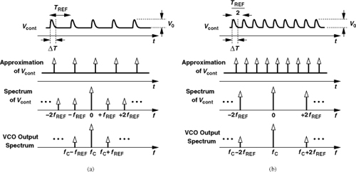
Figure 9.54(a) plots the time-domain and frequency-domain behavior of the control voltage in the first case. Since ΔT ![]() TREF, we approximate each occurrence of the ripple by an impulse of height V0 · ΔT. The spectrum of the ripple thus comprises impulses of height V0 · ΔT/TREF at harmonics of fREF. The two impulses at ±fREF can be viewed in the time domain as a sinusoid having a peak amplitude of 2V0 · ΔT/TREF, producing output sidebands that are below the carrier by a factor of (1/2)(2V0 · ΔT/TREF)KVCO/(2πfREF) = (V0 · ΔTKvco)/(2π).
TREF, we approximate each occurrence of the ripple by an impulse of height V0 · ΔT. The spectrum of the ripple thus comprises impulses of height V0 · ΔT/TREF at harmonics of fREF. The two impulses at ±fREF can be viewed in the time domain as a sinusoid having a peak amplitude of 2V0 · ΔT/TREF, producing output sidebands that are below the carrier by a factor of (1/2)(2V0 · ΔT/TREF)KVCO/(2πfREF) = (V0 · ΔTKvco)/(2π).
Figure 9.54 PLL waveforms and output spectrum for an input period of (a) TREF, (b) TREF/2.
9.5 Phase Noise in PLLs
In our study of oscillators in Chapter 8, we analyzed the mechanism by which device noise translates to phase noise. When an oscillator is phase-locked, its output phase noise profile changes. Also, the reference input to the PLL contains phase noise, corrupting the output. We investigate these effects for type-II PLLs.
9.5.1 VCO Phase Noise
Our understanding of phase-locking suggests that a PLL continually attempts to make the output phase track the input phase. Thus, if the reference input has no phase noise, the PLL attempts to reduce the output phase noise to zero even if the VCO exhibits its own phase noise. From another perspective, as the VCO phase noise accumulates to an appreciable phase error, the loop detects this error and commands the charge pump to briefly turn on and correct it. (If the VCO experienced no phase drift, it would continue to operate at a certain frequency and phase even if the loop were disabled.)
In order to formulate the PLL output noise due to the VCO phase noise, we first derive the transfer function from the VCO phase to the PLL output phase. To this end, we construct the linear phase model of Fig. 9.55(a), where the excess phase of the input is set to zero to signify a “clean” reference. Beginning from the output, we have
![]()
Figure 9.55 (a) Phase-domain model for studying the effect of VCO phase noise, (b) resulting high-pass response.
Using the ζ and ωn expressions developed in Section 9.3.3, we obtain
![]()
As expected, this transfer function has the same poles as Eq. (9.19), but it also contains two zeros at the origin, exhibiting a high-pass behavior [Fig. 9.55(b)].
This result indicates that the PLL suppresses slow variations in the phase of the VCO [small ω in Fig. 9.55(b)] but cannot provide much correction for fast variations. In lock, the VCO phase is compared against the input phase and the corresponding error is converted to current, injected into the loop filter to generate a voltage, and finally applied to the VCO so as to counteract its phase variation. Since both the charge pump and the VCO have nearly infinite gain for slowly-varying signals, the negative feedback remains strong for slow phase variations. For fast variations, on the other hand, the loop gain falls and the feedback provides less correction.
From another perspective, the system of Fig. 9.55(a) can be redrawn as shown in Fig. 9.56(a) and hence Fig. 9.56(b). The system G(s) is equivalent to a cascade of two ideal integrators, thus creating a “virtual ground” at its input (at φout). If φVCO varies slowly, φout is near zero, but as φVCO varies faster, |G(s)| falls and the virtual ground experiences larger swings.
Figure 9.56 Alternative drawings of phase-domain model showing the effect of VCO phase noise.

Solution:
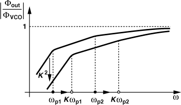
From Eq. (9.22), we observe that both poles scale up by a factor of K. Since ![]() for s ≈ 0, the plot is shifted down by a factor of K2 at low values of ω. Depicted in Fig. 9.57, the response now suppresses the VCO phase noise to a greater extent.
for s ≈ 0, the plot is shifted down by a factor of K2 at low values of ω. Depicted in Fig. 9.57, the response now suppresses the VCO phase noise to a greater extent.
Figure 9.57 Effect of scaling ωn by a factor of K on shaped VCO phase noise.
Solution:
Redrawing the loop of Fig. 9.56(a) as shown in Fig. 9.58(a), we recognize that the feedback is now weaker by a factor of N. The transfer function given by Eq. (9.51) still applies, but both ζ and ωn are reduced by a factor of ![]() .
.
Figure 9.58 (a) Phase-domain model, and (b) shaped VCO phase noise in the presence of a feedback divider.
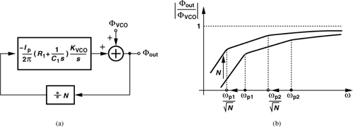
What happens to the magnitude plot of Fig. 9.55(b)? We make two observations. (1) To maintain the same transient behavior, ζ must be constant; e.g., the charge pump current must be scaled up by a factor of N. Thus, the poles given by Eq. (9.22) simply decrease by a factor of ![]() . (2) For S → 0,
. (2) For S → 0, ![]() , which is a factor of N higher than that of the dividerless loop. The magnitude of the transfer function thus appears as depicted in Fig. 9.58(b).
, which is a factor of N higher than that of the dividerless loop. The magnitude of the transfer function thus appears as depicted in Fig. 9.58(b).
Figure 9.59 Time-domain PLL waveforms for (a) equal input and output frequencies, (b) input frequency a factor of N lower.

The PLL output phase noise due to the VCO is equal to the magnitude squared of Eq. (9.51) multiplied by the VCO phase noise. As observed in Chapter 8, oscillator phase noise can be expressed as (α/ω3 + β/ω2), where α and β encapsulate various factors such as the noise injected by devices and the Q, and ω is our notation for the offset frequency (Δω in Chapter 8). Thus,
![]()
We say the VCO phase noise is “shaped” by the transfer function.
It is instructive to study the above phase noise behavior for low and high offset frequencies. At low offset frequencies (slow VCO phase variations), the flicker-noise-induced term is dominant:
![]()
In fact, if ω is sufficiently small, ![]() . That is, the phase noise power rises linearly with frequency. The reader can show that Eq. (9.53) reaches a maximum of
. That is, the phase noise power rises linearly with frequency. The reader can show that Eq. (9.53) reaches a maximum of ![]() at
at ![]() if ζ = 1. Figure 9.60(a) plots this behavior, indicating that the phase-locked VCO exhibits 12 dB less phase noise at
if ζ = 1. Figure 9.60(a) plots this behavior, indicating that the phase-locked VCO exhibits 12 dB less phase noise at ![]() . We recognize that (9.53) approaches α/ω3 at large ω because (9.51) tends to unity.
. We recognize that (9.53) approaches α/ω3 at large ω because (9.51) tends to unity.
Figure 9.60 Effect of PLL on VCO phase noise due to (a) flicker noise, (b) white noise.
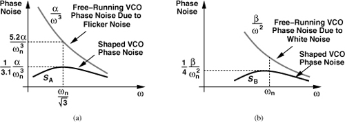
At high offset frequencies, the white-noise-induced term in (9.52) dominates, yielding
![]()
Similarly, this function approaches β/ω2 at sufficiently large ω. The reader can show that (9.54) reaches a maximum of ![]() at ω = ωn if ζ = 1. Figure 9.60(b) plots this behavior, suggesting a 6-dB reduction at ωn. In practice, the overall output phase noise is a combination of these two results.
at ω = ωn if ζ = 1. Figure 9.60(b) plots this behavior, suggesting a 6-dB reduction at ωn. In practice, the overall output phase noise is a combination of these two results.
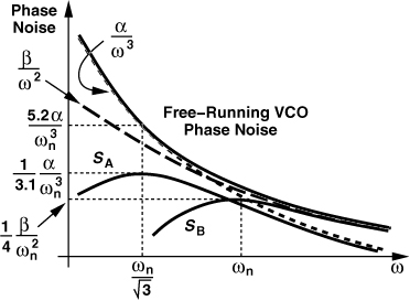
Figure 9.61 summarizes our findings. In addition to the free-running VCO phase noise, the curves corresponding to α/ω3 and β/ω2 are also drawn. The overall PLL output phase noise is equal to the sum of SA and SB. However, the actual shape depends on two factors: (1) the intersection frequency of α/ω3 and β/ω2, and (2) the value of ωn. The following example illustrates these dependencies.
Figure 9.61 Shaped VCO phase noise summary.
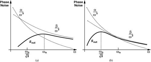
Solution:
Figure 9.62 Shaped VCO phase noise for (a) low, and (b) high intersection frequencies of α/ω3 and β/ω2.
9.5.2 Reference Phase Noise
The reference phase noise is simply shaped by the input/output transfer function of the PLL. From Eq. (9.19), we write
![]()
where SREF denotes the reference phase noise. Note that crystal oscillators providing the reference typically display a flat phase noise profile beyond an offset of a few kilohertz. The overall behavior is shown in Fig. 9.63.
Figure 9.63 Effect of reference phase noise in a PLL.

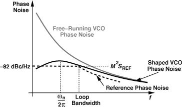
We must now make two important observations. First, PLLs performing frequency multiplication “amplify” the low-frequency reference phase noise proportionally. This can be seen from (9.35) and Example 9.19. That is, Sout = M2SREF within the loop bandwidth. For example, an 802.11g synthesizer multiplying 1 MHz to 2400 MHz raises the reference phase noise by 20 log 2400 ≈ 68 dB. With a typical crystal oscillator phase noise of −150 dBc/Hz, this translates to an output phase noise of about −82 dBc/Hz within the loop bandwidth. A loop bandwidth of around 100 kHz therefore results in the output profile shown in Fig. 9.64.
Figure 9.64 Example of reference and shaped VCO phase noise in a PLL.
The phase noise multiplication can also be analyzed in the time domain: if the input edges are (slowly) displaced by ΔT seconds (2πΔT/TREF radians), then the output edges are also displaced by ΔT seconds, which amounts to 2πΔT/(TREF/N) radians and hence 20 log N decibels of higher phase noise.
Second, the total phase noise at the output (the area under the phase noise profile in Fig. 9.63) increases with the loop bandwidth—a trend opposite of that observed for the VCO phase noise. In other words, the choice of the loop bandwidth entails a trade-off between the reference and the VCO phase noise contributions.
9.6 Loop Bandwidth
As seen in this chapter, the bandwidth of the PLL plays a critical role in the overall performance. Our observations thus far indicate that (1) the settling behavior can be roughly characterized by a time constant in the range of 1/(ζ ωn) and 1/(2ζωn) depending on the value of ζ (Example 9.18); (2) the continuous-time approximation requires that the PLL time constant be much longer than the input period; (3) if the PLL bandwidth increases, the VCO phase noise is suppressed more heavily while the reference phase noise appears across a larger bandwidth at the output.
But how should the loop bandwidth be defined? We can simply compute the −3-dB bandwidth by equating the magnitude squared of Eq. (9.19) to 1/2:
![]()
It follows that
![]()
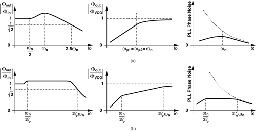
For example, if ζ lies in the range of ![]() and 1, then ω−3dB is between 2.1ωn and 2.5ωn. Also, if 2ζ2
and 1, then ω−3dB is between 2.1ωn and 2.5ωn. Also, if 2ζ2 ![]() 1, then ω−3dB ≈ 2ζωn, as predicted by the one-pole approximation in Section 9.3.4. Figure 9.65(a) plots |φout/φin| and |φout/φVCO| for ζ = 1. Also shown is the shaped VCO phase noise for the white noise regime. Figure 9.65(b) repeats these plots for the case of ζ2
1, then ω−3dB ≈ 2ζωn, as predicted by the one-pole approximation in Section 9.3.4. Figure 9.65(a) plots |φout/φin| and |φout/φVCO| for ζ = 1. Also shown is the shaped VCO phase noise for the white noise regime. Figure 9.65(b) repeats these plots for the case of ζ2 ![]() 1.
1.
Figure 9.65 Frequency responses and shaped VCO phase noise for (a) ζ = 1, and (b) ζ2 ![]() 1.
1.
In the design of PLLs, we impose a loop time constant much longer than the input period, Tin, or a loop bandwidth much smaller than the input frequency to ensure a well-behaved settling. These two constraints, however, are not exactly equivalent. For example, if ζ is around unity, the former translates to
![]()
whereas the latter yields
![]()
Equation (9.59) is a stronger condition and is usually enforced. For higher values of ζ, the loop bandwidth approaches 2ζωn and is set to approximately one-tenth of ωin.
9.7 Design Procedure
The design of PLLs begins with the building blocks: the VCO is designed according to the criteria and the procedure described in Chapter 8; the feedback divider is designed to provide the required divide ratio and operate at the maximum VCO frequency (Chapter 10); the PFD is designed with careful attention to the matching of the Up and Down pulses; and the charge pump is designed for a wide output voltage range, minimal channel-length modulation, etc. In the next step, a loop filter must be chosen and the building blocks must be assembled so as to form the PLL.
In order to arrive at a well-behaved PLL design, we must properly select the charge pump current and the loop filter components. We begin with two governing equations:
![]()
![]()
and choose
Since KVCO is known from the design of the VCO, we now have two equations and three unknowns, namely, Ip, C1, and R1; i.e., the solution is not unique. In particular, the charge pump current can be chosen in the range of a few tens of microamperes to a few milliamperes. With Ip selected, C1 is obtained from (9.61) and (9.63), and R1 from (9.60). Lastly, we choose the second capacitor (C2 in Fig. 9.38) to be about 0.2C1. We apply this procedure to the design of a synthesizer in Chapter 13.
9.8 Appendix I: Phase Margin of Type-II PLLs
In this appendix, we derive the phase margin of second-order and third-order type-II PLLs. Consider the open-loop magnitude and phase response of a second-order PLL as shown in Fig. 9.66. The magnitude falls with a slope of −40 dB/dec up to the zero frequency, ωz = (R1C1)−1, at which the slope changes to −20 dB/dec. The phase begins at −180° and reaches −135° at the zero frequency. To determine the phase margin, we must compute the phase contribution of the zero at the unity-gain frequency, ωu. Let us first calculate the value of ωu.
![]()
Figure 9.66 Open-loop magnitude and phase response of type-II PLL.
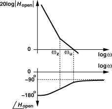
![]()
Using Eqs. (9.20) and (9.21) as short-hand notations and noting that ![]() , we have
, we have
![]()
and
![]()
The phase margin is therefore given by
For example, if ζ = 1, then PM = 76° and ωu/ωz ≈ 4, and if ![]() , then PM = 65° and ωu/ωz ≈ 2.2. For
, then PM = 65° and ωu/ωz ≈ 2.2. For ![]() , we have
, we have ![]() and hence
and hence
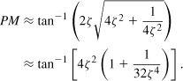
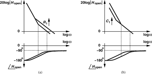
Solution:
As R1 increases, ωz falls but ωu rises (because the slope of |Hopen| must still be equal to −20 dB/dec) [Fig. 9.67(a)]. On the other hand, as C1 increases, ωz falls and ωu remains relatively constant [Fig. 9.67(b)]. This is because, for ζ ≥ ![]() ,
,


Figure 9.67 Effect of (a) higher R1, or (b) higher C1 on frequency response of type-II PLL.
Let us now consider the third-order loop of Fig. 9.38. The reader can show that the PFD/CP/filter cascade provides the following transfer function:
![]()
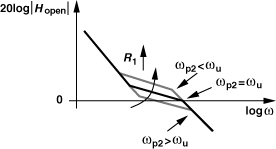
where Ceq = C1C2/(C1 + C2). The pole contributed by the filter, ωp2, thus lies at −(R1Ceq)−1. Figure 9.68(a) plots an example of the open-loop frequency response, revealing the PM degradation due to C2.
Figure 9.68 Effect of second capacitor on PLL open-loop response for (a) ωp2 = (R1Ceq)−1 < ωu, and (b) ωp2 = (R1Ceq)−1 > ωu.
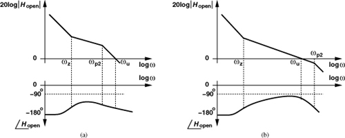
How should ωp2 be chosen? If located below ωu, this pole yields a PM of less than 45°. This is because the phase profile shown in Fig. 9.68(a) experiences a contribution of −45° from ωp2 at ωp2 and hence a more negative amount at ωu. For this reason, ωp2 must be chosen higher than ωu [Fig. 9.68(b)]. The key point here is that the magnitude of ωu is roughly the same even in the presence of ωp2, allowing the use of Eq. (9.73).
The phase margin can now be calculated as
In most cases of practical interest, 32ζ2 ![]() 1 and hence
1 and hence
![]()
Note that this result is valid only if ζ ≥ 1 and ωp2 is well above ωu.
An alternative approach seeks that value of ωu which maximizes the PM in Eq. (9.78) [10]. Differentiation yields
![]()
and
![]()
The corresponding ζ can be obtained by differentiating Eq. (9.80):
![]()
approximately equal to 0.783 for C1 = 5C2.
The foregoing study also reveals another important limitation in the choice of the loop parameters: with C2 present, R1 cannot be arbitrarily large. After all, if R1 → ∞, the series combination of R1 and C1 vanishes, leaving only C2 and hence only two ideal integrators in the loop. To determine an upper bound on R1, we note that, as R1 increases, ωp2 approaches and eventually falls below ωu (Fig. 9.69). If we consider ωp2 ≈ ωu as the lower limit on ωp2, then
Figure 9.69 Effect of higher R1 on PLL frequency response in the presence of second capacitor.
It follows that
![]()
and hence
![]()
We note that, if ζ ≈ 1 and C2 ≈ 0.2C1, this condition is satisfied.
References
[1] F. M. Gardner, Phaselock Techniques, Second Edition, New York: Wiley & Sons, 1979.
[2] B. Razavi, Design of Analog CMOS Integrated Circuits, Boston: McGraw-Hill, 2001.
[3] J. P. Hein and J. W. Scott, “z-Domain Model for Discrete-Time PLLs,” IEEE Trans. Circuits and Systems, vol. 35, pp. 1393–1400, Nov. 1988.
[4] J. Alvarez et al., “A Wide-Bandwidth Low-Voltage PLL for PowerPC Microprocessors,” IEEE J. of Solid-State Circuits, vol. 30, pp. 383–391, April 1995.
[5] J. M. Ingino and V. R. von Kaenel, “A 4-GHz Clock System for a High-Performance System-on-a-Chip Design,” IEEE J. of Solid-State Circuits, vol. 36, pp. 1693–1699, Nov. 2001.
[6] B. J. Hosticka, “Improvement of the Gain of CMOS Amplifiers,” IEEE J. of Solid-State Circuits, vol. 14, pp. 1111–1114, Dec. 1979.
[7] J.-S. Lee et al., “Charge Pump with Perfect Current Matching Characteristics in Phase-Locked Loops,” Electronics Letters, vol. 36, pp. 1907–1908, Nov. 2000.
[8] M. Terrovitis et al., “A 3.2 to 4 GHz 0.25 μm CMOS Frequency Synthesizer for IEEE 802.11a/b/g WLAN,” ISSCC Dig. Tech. Papers, pp. 98–99, Feb. 2004.
[9] M. Wakayam, “Low offset and low glitch energy charge pump and method of operating same,” US Patent 7057465, April 2005.
[10] H. R. Rategh, H. Samavati, and T. H. Lee, “A CMOS Frequency Synthesizer with an Injection-Locked Frequency Divider for a 5-GHz Wireless LAN Receiver,” IEEE J. of Solid-State Circuits, vol. 35, pp. 780–788, May 2000.
Problems
9.1. The mixer phase detector characteristic shown in Fig. 9.5 exhibits a zero gain at the peaks, e.g., at Δφ = 0. A PLL using such a PD would therefore suffer from a zero loop gain at these points. Does this mean the PLL would not lock?
9.2. If KVCO in the PLL of Fig. 9.10(a) is very high and the PD has the characteristic shown in Fig. 9.5, can we estimate the value of Δφ?
9.3. Repeat Problem 9.2 if the sign of KVCO is changed.
9.4. Determine at what frequencies the output sidebands of Fig. 9.7(a) are located. Are these sidebands or harmonics?
9.5. In the PLL of Fig. 9.8(b), an input change of Δφ exactly yields an output change of Δφ. On the other hand, in the buffer of Fig. 9.8(a), an input change of ΔV produces an output change of ΔV/(A0 + 1), where A0 is the open-loop gain of the op amp. How do we explain this difference?
9.6. Suppose the PLL of Fig. 9.12 is locked. Now, we replace R1 with an open circuit. What happens at the output as time passes? Consider two cases: a noiseless VCO and a noisy VCO. This example shows that if the VCO (excess) phase does not drift with time, the feedback loop can be broken.
9.7. Determine the transfer function, ζ, and ωn for the frequency-multiplying PLL of Fig. 9.18(b).
9.8. For the PFD of Fig. 9.20, determine whether or not the average value of QA − QB is a linear function of the input frequency difference.
9.9. Compute the peak value of |H| in Example 9.17.
9.10. Suppose a PLL designed with ζ = 1, a loop bandwidth of ωin/25, and a tuning range of 10%. Assume Vcont can vary from 0 to VDD. Prove that that the voltage drop across the loop filter resistor reaches roughly 1.6πVDD if no second capacitor is used.
9.11. A PLL is designed with an input frequency of 1 MHz and an output frequency of 1 GHz. Now suppose the design is modified to operate with an input frequency of 2 MHz. Explain from Eq. (9.43) what happens to the output sidebands if (a) the output frequency remains unchanged, or (b) the output frequency also doubles. Assume in the latter case that KVCO must double.
9.12. The ripple on the control voltage creates sidebands around the carrier at the output of a PLL, equivalently disturbing the phase of the VCO. Explain why the PLL suppresses the VCO phase noise (within the loop bandwidth) but not the sidebands due to the ripple.
9.13. Consider the PLL shown in Fig. 9.70, where amplifier A1 is interposed between the filter and the VCO. If the amplifier exhibits an input-referred flicker noise density given by α/f, determine the PLL output phase noise.
Figure 9.70 PLL with amplifier in the loop.
9.14. A PLL incorporates a VCO having the characteristic shown in Fig. 9.71. It is possible to compensate for the VCO nonlinearity by varying the charge pump current as a function of the control voltage so that the loop dynamics remain relatively constant. Sketch the desired variation of the charge pump current.
Figure 9.71 Nonlinear characteristic of a VCO.

9.15. A PLL operates with input and output frequencies equal to f1. Suppose the input frequency and hence the output frequency are changed to f1/2. Assuming all loop parameters remain unchanged and neglecting the continuous-time approximation issues, explain which one of these arguments is correct and why the other one is not:
(a) The PFD now makes half as many phase comparisons per second, pumping half as much charge into the loop filter. Thus, the loop is less stable.
(b) Equation ![]() indicates that ζ remains constant and the loop is as stable as before.
indicates that ζ remains constant and the loop is as stable as before.
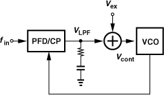
9.16. In the loop shown in Fig. 9.72, Vex suddenly jumps by ΔV. Sketch the waveforms for Vcont and VLPF and determine the total change in Vcont, VLPF, the output frequency, and the input-output phase difference.
Figure 9.72 PLL with a step on the control voltage.
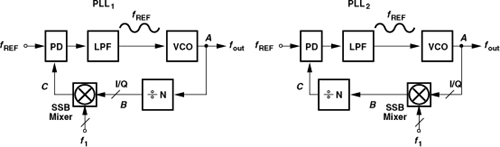
9.17. Two PLL configurations are shown in Fig. 9.73. Assume the SSB mixer adds its input frequencies. Also, assume f1 is a constant frequency provided externally and it is less than fREF. The control voltage experiences a small sinusoidal ripple with a frequency of fREF. Both PLLs are locked.
(a) Determine the output frequencies of the two PLLs.
(b) Determine the spectrum at point A due to the ripple.
(c) Now determine the spectrum at nodes B and C.
Figure 9.73 Two PLL topologies.