
3
Synthesizing Hardware from a State Diagram
3.1 INTRODUCTION TO FINITE-STATE MACHINE SYNTHESIS
At this point, the main requirements to design an FSM have been covered. However, the ideas discussed need to be practised and applied to a range of problems. This will follow in later chapters of the book and provide ways of solving particular problems.
In the development of a practical FSM there is a need to be able to convert the state diagram description into a real circuit that can be programmed into a PLD, FPGA, or other application-specific integrated circuit (ASIC). As it turns out, this stage is very deterministic and mechanized.
FSM synthesis can be performed at a number of levels.
Develop an FSM using flip-flops, which can be:
- D-type flip-flops;
- T-type flip-flops;
- JK-type flip-flops.
Use a high-level HDL such as VHDL. This can be used to enter the state diagram directly into the computer. The HDL can then be used to produce a design based upon any of the above flip-flop types using one of a number of technologies.
It is also possible to take the state diagram and convert it into a C program and, hence, produce a solution suitable for implementation using a micro-controller.
By using the direct synthesis approach, or an HDL, the final design can be implemented using:
- discrete transistor–transistor logic (TTL) or complementary metal oxide–semiconductor (CMOS) components (direct synthesis);
- PLDs;
- FPGAs;
- ASICs;
- a very large-scale integration chip.
Most technologies support D- and T-type flip-flops, and in practice these devices are used a lot in industrial designs; therefore, this book will look at the way in which T flip-flops and D flip-flops can be used in a design. Note: JK flip-flops can also be used, but these are not covered in this book.
This chapter will look at the implementation of an FSM using T-type flip-flops and then move on to look at designs using D-type flip-flops.
Why T- and D-type flip-flops?
These are the most common types of flip-flop used today. The reason is that the T type can be easily implemented from a D type, and the D type requires only six gates (compared with the JK type, which requires about 10 gates). This means that D-type flip-flops occupy less chip area than JK types. Another reason is that the D-type flip-flop is more stable than the JK flip-flop.
D-type flip-flops are naturally able to reset, in that if the D input is at logic 0, then the flip-flop will naturally reset on the next clock input pulse (see later on in this chapter). This can be of great benefit in the design of FSMs.
Go to Frame 3.1 to find out how to use the T flip-flop.
3.2 LEARNING MATERIAL
Frame 3.1 The T-type flip-flop
A T-type flip-flop can be implemented with a standard D-type flip-flop, as illustrated in Figure 3.1.
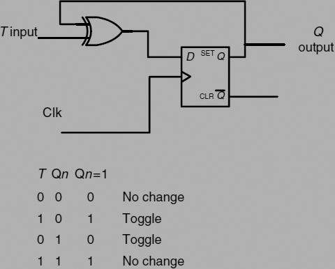
Figure 3.1 Diagram and characteristics of a T flip-flop.
As can be seen from the diagram, the T flip-flop is implemented by using a D flip-flop with an exclusive OR gate. The table under the flip-flop shows its characteristics.
In this table, Qn is the present state output of the flip-flop (prior to a clock pulse), whilst Qn + 1 is the next state output of the flip-flop (after the clock pulse). The table shows that the flip-flop will change state on each clock pulse provided that the t input is high. But if the T input is low, then the flip-flop will not change state.
Therefore, use the t input to control the flip-flop, since, whenever the flip-flop is to change state, simply set the t input high; otherwise it is held low.
Go to Frame 3.2.
Frame 3.2 The T flip-flop example
Consider the simple single-pulse generator with memory example of Frame 1.13 reproduced in Figure 3.2.
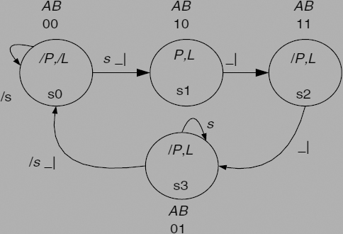
Figure 3.2 State diagram for the single-pulse generator with memory.
Follow the state transitions for secondary state variable A and write down the state term wherever there is a 0-to-1 or a 1-to-0 transition in A. In the above state diagram there is a 0-to-1 transition in A between states s0 and s1, and a 1-to-0 transition between states s2 and s3. Therefore, write down
A · T = s0 · s + s2.
This equation defines the logic that will be connected to the T input of flip-flop A.
Whenever the FSM is in state s0, and input s is high, the T input of flip-flop A will be high. Whenever the T input is high, the flip-flop will toggle. Since in state s0 both flip-flops are reset, then in state s0, when s goes to logic 1, the next clock pulse will cause the flip-flop A to go from 0 to 1.
In state s1, the T input to flip-flop A will be at logic 0 since there is no term to hold this input high in these states. Therefore, in state s1 the flip-flop A will not toggle with the clock pulse. When the FSM reaches state s2, the T input will go high again and the next clock pulse will cause the flip-flop to toggle back to its reset state as intended. Note that in state s3 the T input to flip-flop A will be low again, so the flip-flop will not toggle on the next clock pulse in state s3.
Note that the equation for A · T uses the present state condition to set the t line high. This is necessary in order to make sure that the flip-flop will toggle on the next clock pulse. The logic being produced here, therefore, is that of the next state decoder of the FSM (see Frame 1.4).
| Task | Try producing the equation for the input logic for the T input on flip-flop B. |
Then go to Frame 3.3 to see the solution.
The equation for the T input of flip-flop B is
B · T = s1 + s3 · /s.
Since in state s1 the B · T input needs to be logic 1, so that on the next clock pulse the flip-flop will change from a reset state to a set state. Note that there is no outside world input condition between states s1 and s2.
The second term s3 · /s will cause the B flip-flop to toggle from its set state to its reset state in state s3 when the outside world input s = 0 on the next clock pulse.
In summary, look for the 0-to-1 or 1-to-0 transition in each flip-flop.
| Task | Now try the example in Figure 3.3 and also produce the output equations for this design, but with output L being high in s3 only if a new input R is logic 1. |
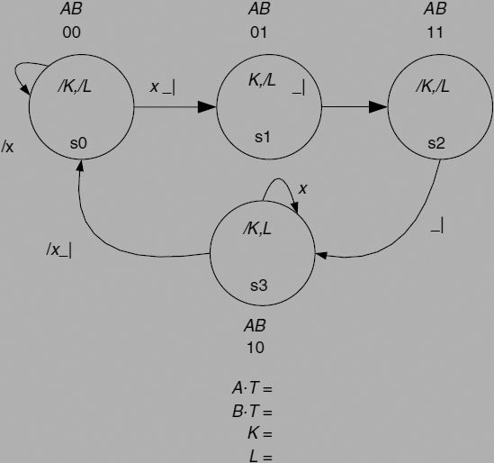
Figure 3.3 State diagram example for implementation using T flip-flops.
Now turn to Frame 3.4.
The modified state diagram is shown in Figure 3.4.
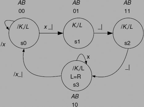
Figure 3.4 State diagram example for implementation using T flip-flops.
The equations for A · T and B · T are
A · T = s1 + s3 · /x
B · T = s0 · x + s2.
The outside world outputs are
K = s1 = /A · B
L = s3 · R = A · /B · R.
The equation for L is a Mealy output in which the value of L can only be logic 1 in state s3, but only if input R is also logic 1. Refer to Frames 3.1–3.3 for the method if necessary.
Please now turn to Frame 3.5.
| Task | Attempt the following examples. Produce the flip-flop equations and output equations for each of the state diagrams indicated. If you are not too sure, reread Frames 3.1–3.4 before starting to do the problems. |
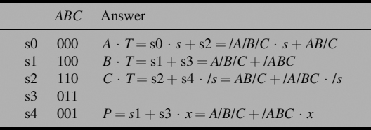
State diagram in Frame 1.19, Figure 1.22, using the following secondary state variables:
| ABC | |
| s0 | 000 |
| s1 | 100 |
| s2 | 110 |
| s3 | 011 |
| s4 | 001 |
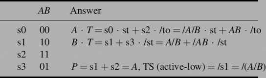
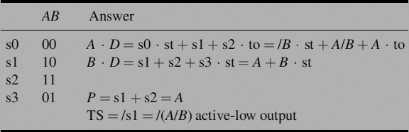
State diagram in Frame 2.3, Figure 2.4, using the following secondary state variables:
| AB | |
| s0 | 00 |
| s1 | 10 |
| s2 | 11 |
| s3 | 01 |
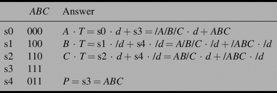
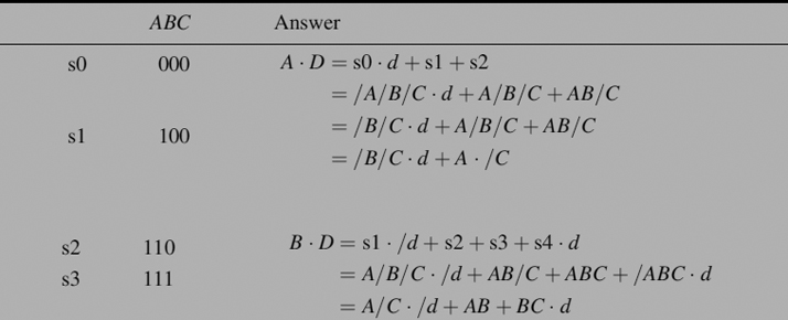
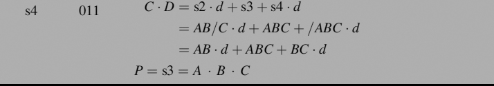
State diagram in Frame 2.12, Figure 2.13, using the following secondary state variables:
| ABC | |
| s0 | 000 |
| s1 | 100 |
| s2 | 110 |
| s3 | 111 |
| s4 | 011 |
| s5 | 001 |
State diagram in Frame 2.9, Figure 2.10, using the following secondary state variables:
| ABCD | |
| s0 | 0000 |
| s1 | 1000 |
| s2 | 1100 |
| s3 | 1110 |
| s4 | 1111 |
| s5 | 0111 |
| s6 | 0011 |
| s7 | 1011 |
| s8 | 1001 |
| s9 | 0001 |
See Frame 3.6 for the solution to these problems.
The answers to the problems in Frame 3.5 are as follows.
For the state diagram of Frame 1.19, Figure 1.22:
For the state diagram of Frame 2.3, Figure 2.4:
For the state diagram of Frame 2.12, Figure 2.13:
For the state diagram of Frame 2.9, Figure 2.10:
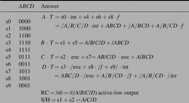
If you are having difficulty in seeing how the active-low output equations are obtained, skip forward to Frame 3.25 (and Frame 3.26) for an explanation, then return to this frame.
| Task | Finally, try producing the equations for the state diagram of Frame 2.14, Figure 2.16; it has already been assigned secondary state variables. The answer is in Frame 3.7. |
The answers for the state diagram of Frame 2.14, Figure 2.16 are
The complete cycle of designing an FSM and synthesizing it using T-type flip-flops has been completed.
T-type flip-flops, as has already been seen in Frame 3.1, can be implemented from a basic D-type flip-flop, using an exclusive OR gate. Some PLDs support both the D- and T-type flip-flops, so FSM designs can be implemented using these PLDs.
Some PLD devices can be programmed to be either D-type or T-type flip-flops. However, most PLD devices support D-type flip-flops, particularly the cheaper PLD devices, such as the 22v10. Therefore, it is worthwhile considering how D-type flip-flops can be used to synthesize FSMs.
As it turns out, using D-type flip-flops to synthesize FSMs requires a little thought, so some time will be spent looking at the techniques required in order to make use of D-type flip-flops in the design of FSMs. This will be time well spent, since it opens up a large number of potential devices that can be used to design FSMs.
Turn to Frame 3.8.
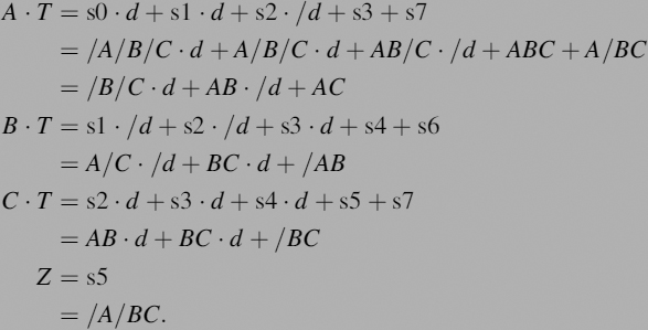
Frame 3.8 Synthesizing FSMs using D-type flip-flops: the D-type flip-flop equations
Consider the basic D flip-flop device shown in Figure 3.5.
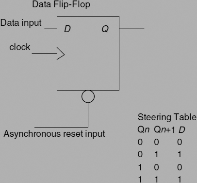
Figure 3.5 Diagram and characteristics of a D flip-flop.
The D-type flip-flop has a single data input D (apart from the clock input).
- The data line must be asserted high before the clock pulse, for the Q output to be clocked high by the 0-to-1 transition of the clock.
- For the Q output to remain high, the D input must be held high so that subsequent clock pulses will clock the 1 on the D input into the Q output.
These two bullet points are very important and should be remembered when using D-type flip-flops.
Consider the waveforms shown in Figure 3.6 applied to a D flip-flop.
Figure 3.6 Incomplete timing diagram for a D flip-flop.
| Task | Complete the timing diagram for the output Q. |
| Hint: | study the content of this frame and the steering table. |
Go to Frame 3.9 after completing the diagram.
The completed timing diagram is illustrated in Figure 3.7.
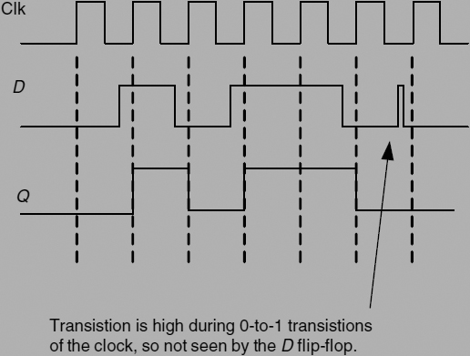
Figure 3.7 Complete timing diagram for a D flip-flop.
The trick here is to look at the value of the D line whenever the clock input makes a transition from 0 to 1; whatever the D line logic level is, the Q output level becomes.
This is because the D-type flip-flop sets its Q output to whatever the D input logic level is at the time of the clock 0-to-1 transition.
In the timing waveform, the D input is held high over two clock periods. This means that the Q output will also be held high over the same two clock periods.
Note the point on the timing waveform when the D input makes a transition to logic 1 for a brief period (between clock pulses). The flip-flop is unable to see this transition of the D input, so the flip-flop is unable to respond.
Note: the flip-flop can only update its Q output at the 0-to-1 transition of the clock input.
Go to Frame 3.10.
Having covered the basics of the D flip-flop, consider the state diagram in Figure 3.8.
It is, of course, the single-pulse generator with memory FSM seen in Frame 1.13. This will be synthesized using D-type flip-flops.
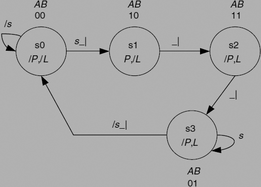
Figure 3.8 State diagram for implementing using D flip-flops.
The equation for flip-flop A is
A · D = s0 · s + s1 = /A /B · s + A · /B = /B · s + A · /B (using Aux rule).
Note, the D line of flip-flop A needs to be set in state s0 and held set over state s1.
Now consider the equation for flip-flop B:
B · D = s1 + s2 + s3 · s = A · /B + A · B + /A · B · s = A + /A · B · s = A + B · s.
The first term sets the D line high in state s1, whilst the second term holds the D line high over state s2. But what is happening in the third term?
In state s3 the D line needs to be held high if the input s is not logic 1, since when s = 0 the FSM should return to state s0 (by resetting flip-flop B). Therefore, whilst s = 1, the third term in the equation for B · D will be high. When s = 0, this term will become logic 0 and the B flip-flop will reset, causing the FSM to move to state s0.
Negate the input term (s in this case) with s3 to hold the D input of the flip-flop high.
| Rule 1 | Whenever there is a 1-to-0 transition with an input term present along a transitional line of the state diagram, then AND the state with the negated input. |
Turn to Frame 3.11.
Now consider the state diagram shown in Figure 3.9.
This is just a modification of the single-pulse generator FSM which allows the FSM to produce multiple pulses if input k = 1 and m = 1, and multiple pulses every four clock cycles if k = 1 and m = 0.

Figure 3.9 State diagram with two-way branch.
The equation for the A flip-flop is
A · D = s0 · s + s1 + s2 · m.
The first term is to set the A · D input high for the next clock pulse to set the flip-flop and cause the FSM to move into state s1.
The second term is to hold the flip-flop set between states s1 and s2. Note that the input term along the transitional line between state s1 and s2 (k) is not present in the second term. This is because it is not needed. The flip-flop is to remain set regardless of the state of the input k.
| Rule 2 | A term denoting a transition between two states where the flip-flop remains set does not need to include the input term. |
The third term in the equation for A · D is a bit more complicated. This term is a holding term for the two-way branch state s2. In state s2, the transitional path between states s2 and s3 is a 1-to-0 transition. Therefore, apply Rule 1 (defined in Frame 3.10). The term is therefore s2 · m. The other path, between states s2ands1, is a 1-to-1 transition. Note: the term denoted by the s2 to s1 transition is not present in the equation for A · D. This is because it is not required. The third rule is as follows.
| Rule 3 | A two-way branch in which one path is a 1-to-0 transition and the other a 1-to-1 transition will always produce a term involving the state and the 1-to-0 transition with the input along the 1-to-0 transitional line negated. The 1-to-1 transitional path will be ignored. |
Go to Frame 3.12.
To see why these three rules apply, look at the state diagram of Frame 3.11 again, which is reproduced in Figure 3.10 for convenience.
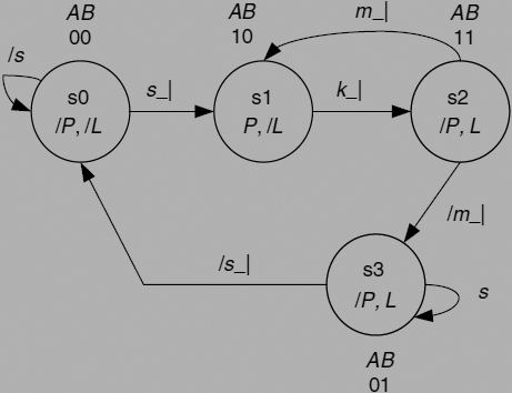
Figure 3.10 State diagram with two-way branch.
| Rule 1 | Whenever there is a 1-to-0 transition with an input term present along a transitional line of the state diagram, the state is ANDed with the negated input. |
A 1-to-0 transition with an input along the transitional line connecting the two states needs to be ANDed with the negated input condition along the transitional line in order to hold the flip-flop set until the input condition along the transitional line becomes true.
A 1-to-0 transition without an input along the transitional line connecting the two states does not need to be included in the equation, since the FSM will always be able to follow the transition and the flip-flop will always be able to reset.
| Rule 2 | A term denoting a transition between two states where the flip-flop remains set does not need to include the input term. |
In the above state diagram the transition between state s1 and s2 for flip-flop A is s1 · k + s1 · /k, i.e. it does not matter what state the input k is since A is to remain 1 regardless of whether it is in state s1 or s2. Therefore, s1 · k + s1 · /k = s1 by Boolean logical adjacency rule.
| Rule 3 | A two-way branch in which one path is a 1-to-0 transition and the other a 1-to-1 transition will always produce a term involving the state and the 1-to-0 transition with the input along the 1-to-0 transitional line negated. The 1-to-1 transitional path will be ignored. |
In the above state diagram the two-way branch involves a 1-to-0 transition and a 1-to-1 transition. In state s2, flip-flop A will remain set if m = 1 and must reset if m = 0.
Go to Frame 3.13.
The diagram in Figure 3.11 illustrates all possible conditions for a two-way branch in a state diagram.
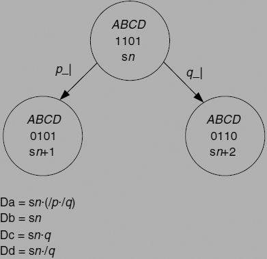
Figure 3.11 State diagram segment showing different conditions in a two-way branch.
In particular, note the condition for flip-flop A in a two-way branch with both transitions being 1 to 0. The term DA = sn · (/p · /q) implies that the negation of the input term along each transitional line is being used. Only if both p = 0 and q = 0 will the FSM remain in state sn.
Study the diagram carefully and then go to Frame 3.14.
Look at the state diagram segments shown in Figure 3.12.
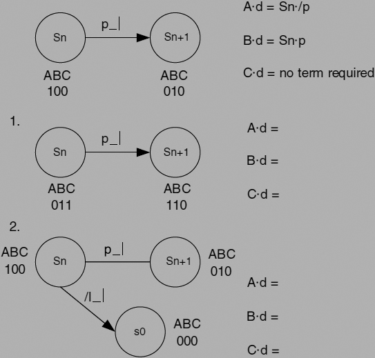
Figure 3.12 Some two-way branch examples for the reader.
| Task | Complete the two sets of D flip-flop equations. |
When these have been completed, go to Frame 3.15.
The answers to the two problems in Frame 3.14 are as follows:
- A · D = sn · P
B · D = sn
C · D = sn · /P.
- A · D = sn · /P · l, since both p = 0 and l = 1 are needed to stay in sn
B · D = sn · p, since there is a 0-to-1 transition between sn and sn + 1
C · D, no term required.
Refer to Frames 3.8–3.14 for the method if required. Now try the following problem.
| Task | The FSM illustrated in Figure 3.13, which is to be synthesized with D-type flip-flops, has two states with two-way branches. Produce the equations for the two D flip-flops, as well as the output equation for X. |
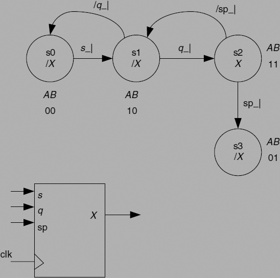
Figure 3.13 An example with multiple two-way branches.
Go to Frame 3.16 after completing this example.
The solution to the problem in Frame 3.15 is
A · D = s0 · s + s1 · q + s2 · /sp.
Since s0 · s is a set term, s1 · q is the 1-to-0 transition between s1 and s0, and s2 · /sp is the 1-to-0 transition between s2 and s3:
B · D = s1 · q + s2 · sp + s3.
Since s1 · q is the set term, s2 · sp is the 1-to-0 transition holding term between s2 and s1, and s3 is the holding term in state s3. Note that there is no way of leaving state s3. The output equation is X = s2, which makes the FSM a Moore FSM because the output is a function of the secondary state variables.
To provide a way out of s3, and to provide an initialization mechanism, it is wise to provide a reset input to all FSMs. In any case, one should always provide a means of initializing the FSM to a known state.
Resetting the flip-flops
If the flip-flops have asynchronous reset inputs (see Figure 3.14), then this is easily accomplished by a common connection to all reset inputs.
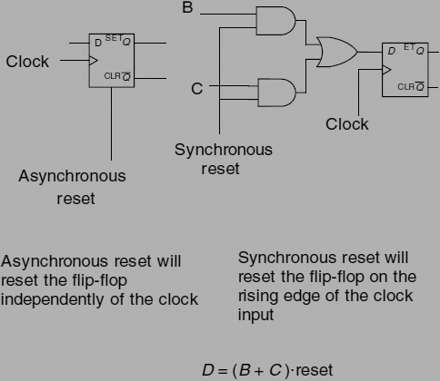
Figure 3.14 Circuit diagrams showing asynchronous and synchronous resetting of a D flip-flop.
If the flip-flops do not have an asynchronous reset input (or any reset input), then a synchronous reset can be provided by ANDing a reset input to each D input. In the case of the synchronous input, the reset line (which is active-low) is normally held high; this enables the logic for each flip-flop D input. Lowering the reset line disables the AND gates and results in the D inputs also going low. The next clock pulse, therefore, will cause the flip-flops to reset. Note that the flip-flops will reset on the rising edge of the clock pulse for positive-edge-triggered flip-flops.
Go to Frame 3.17.
| Task | Try producing the D flip-flop equations and the output equations for each of the following state diagrams. If you are not too sure, then reread Frames 3.8 to 3.16 again before starting to do the problems. |
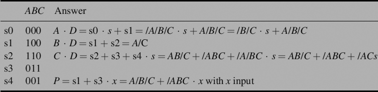
State diagram in Frame 1.19, Figure 1.22, using the following secondary state variables:
| ABC | |
| s0 | 000 |
| s1 | 100 |
| s2 | 110 |
| s3 | 011 |
| s4 | 001 |
State diagram in Frame 2.3, Figure 2.4, using the following secondary state variables:
| AB | |
| s0 | 00 |
| s1 | 10 |
| s2 | 11 |
| s3 | 01 |
State diagram in Frame 2.12, Figure 2.13, using the following secondary state variables:
| ABC | |
| s0 | 000 |
| s1 | 100 |
| s2 | 110 |
| s3 | 111 |
| s4 | 011 |
State diagram in Frame 2.9, Figure 2.10, using the following secondary state variables:
| ABCD | |
| s0 | 0000 |
| s1 | 1000 |
| s2 | 1100 |
| s3 | 1110 |
| s4 | 1111 |
| s5 | 0111 |
| s6 | 0011 |
| s7 | 1011 |
| s8 | 1001 |
| s9 | 0001 |
See Frame 3.18 for the solution to these problems.
The solutions to the problems in Frame 3.17 are as follows.
State diagram in Frame 1.19, Figure 1.22:
State diagram in Frame 2.3, Figure 2.4:
State diagram in Frame 2.12, Figure 2.13:
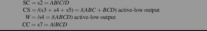
State diagram in Frame 2.9, Figure 2.10:
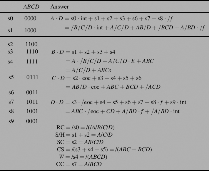
Note: active-low outputs are shown here with right-hand side negated.
| Task | Once these have been completed, try taking the single-pulse generator example of Frame 3.10, Figure 3.8, and produce the D-type flip-flop equations and output equations. Finally, produce a circuit diagram for the FSM using D-type flip-flops with asynchronous reset inputs and other logic gates. When complete, go to Frame 3.19. |
The complete design for the single-pulse generator with memory is given below;
The design equations
A · D = s0 · s + s1 = A /B + /B · s
B · D = s1 + s2 + s3 · s = A + B · s
P = s1 = A/B and L = B.
The circuit diagram of Figure 3.15 shows the memory elements (flip-flops), input decoding logic (A · D and B · D logic), and output decoding logic (for the output P).
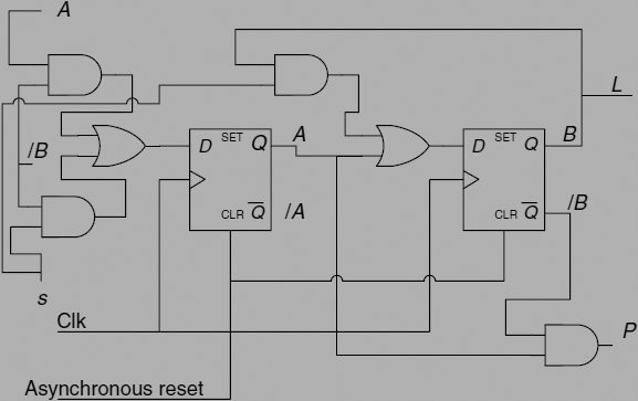
Figure 3.15 Circuit for the single-pulse generator with memory using an asynchronous reset.
If flip-flops with asynchronous reset inputs are not available, then a synchronous reset can be used, ANDed with the A · D and B · D logic, as illustrated in Figure 3.16.
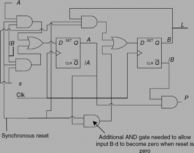
Figure 3.16 Circuit for the single-pulse generator with memory using a synchronous reset.
In this illustration, the reset line is connected to the AND logic of each D input. Note the addition of the extra AND gate to the input logic of B · D so that when reset = 0, B · D = 0also.
Go to Frame 3.20.
So now, all aspects of designing FSMs have been covered: from initial specification, to construction of the state diagram, to synthesizing the circuit used to implement the FSM. A run through the complete design process will now be undertaken. Consider these steps for the single-pulse generator FSM.
The Specification
The block diagram showing inputs and outputs is first constructed (Figure 3.17). This would be supplemented with a written specification describing the required behaviour of the FSM.
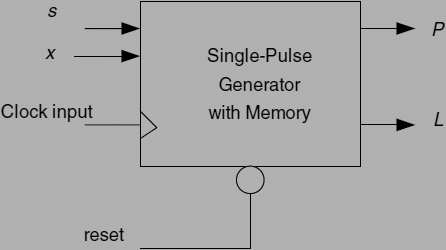
Figure 3.17 Block diagram for the single-pulse generator with memory.
‘The FSM is to produce a single pulse at its output P whenever the input s goes high. No other pulse should be produced at the output until s has gone low, then high again. In addition, an output L is to indicate that the P pulse has taken place, to be cancelled when s goes low. The L output can be disabled by asserting input x to logic 1.’
The next step is to produce the state diagram. This is not a trivial step, since it requires the use of a number of techniques developed during this programme of work. This is the skilled part of the development process.
Go to Frame 3.21.
The state diagram is shown in Figure 3.18.
Now assign secondary state variables to the state diagram in order to continue with the synthesis of the FSM. Then, develop the equations for the flip-flops next state decoder, and output logic.
The design equations
A · D = (s0 · s + s1) · reset = (A/B + /B · s) · reset
B · D = (s1 + s2 + s3 · s) · reset =(A + B · s) · reset
P = s1 = A/B
L = s2 · x + s3 · x = B · x.
Finally, the circuit is produced from the equations (Figure 3.19). Note that output L is a Mealy output because it used the input x.
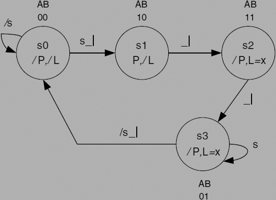
Figure 3.18 State diagram for the single-pulse generator with memory.
The design can then be simulated to ensure that it is functioning according to the original specification.
Simulation
Note here that the output L is conditional upon input x, so that it can only be logic 1 in states s2 and s3, and then only if input x is logic 1 also. This is illustrated in the waveforms in Figure 3.20.
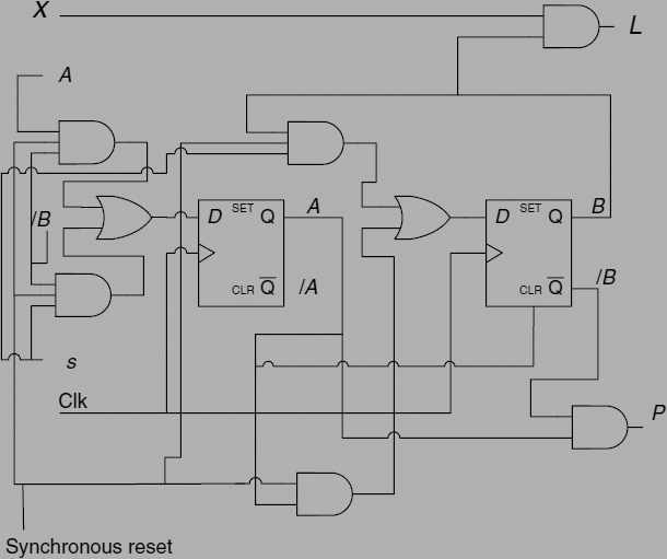
Figure 3.19 Circuit diagram of the single-pulse generator with memory.
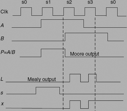
Figure 3.20 Timing diagram for the single-pulse generator with memory.
Go to Frame 3.22.
In some cases there is a need to use three-way (or more) branches. This has been avoided up until now, but the rules can be used to resolve all pathways. However, each path must be mutually exclusive.
Consider the diagram in Figure 3.21.
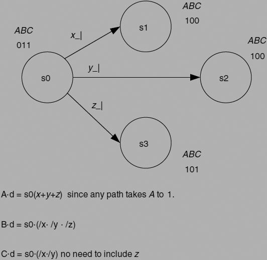
Figure 3.21 State diagram segment with three-way branch.
Here, the input A · d for flip-flop A has 0-to-1 transition in all three paths. To meet the requirements for the D flip-flop, all leaving terms (x, y, and z) need to be logically ORed to provide a transition when any input becomes active.
In the case of B · d there are three 1-to-0 transition paths; this can be dealt with by using the 1-to-0 negation rule for all three paths, as shown.
In the case of C · d there are two 1-to-0 transitions and one 1-to-1 transition. In this case the 1-to-0 negate rule is applied to the two 1-to-0 transition paths, both ANDed because they both have to be true to keep the FSM in s0. The 1-to-1 transition is, as usual, ignored.
Go to Frame 3.23.
| Task | Consider the state diagram fragment in Figure 3.22. |
| Complete the equations for A · d, B · d, and C · d. |
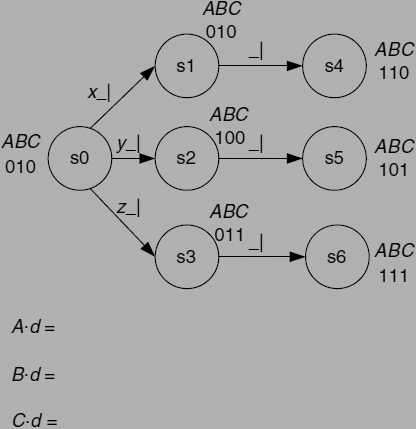
Figure 3.22 Incomplete three-way branch example.
When completed, go to Frame 3.24.
The three equations are illustrated in Figure 3.23.
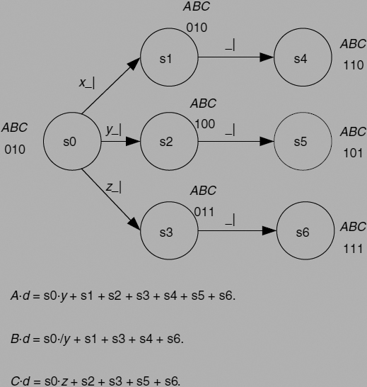
Figure 3.23 Solution to the three-way branch example.
In the equation for B · D, the term s0 · /y is keeping the FSM in state s0. In the equation for C · D, the term s0 · z will hold the FSM in state s0 until z = 1. So the rules for D flip-flops developed earlier still apply.
Go to Frame 3.25.
Frame 3.25 Recap on how to deal with multistate Moore active-low outputs
In some state diagram designs there is a need to write an output equation in its ‘active-low’ form rather than in its ‘active-high’ form. This is particularly true when controlling memory devices, where the chip select line from the FSM to the memory device is often active-low. If this signal was dealt with as an active-high signal, then all states where the chip select line was not active would have to be written into the equation for chip select (CS).
The illustration in Figure 3.24 shows a typical example.
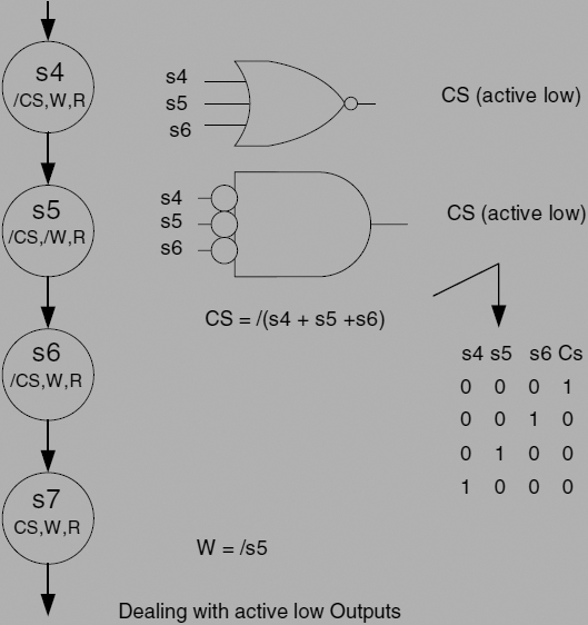
Figure 3.24 Dealing with active-low inputs.
In this example, CS is logic 0 (active) in states s4, s5 and s6, but high again in state s7.
The three states s4, s5 and s6 are all ORed and the whole OR expression inverted (NOR). This can, if preferred, be written either in the NOR form, or, by applying De Morgan's rule in the form of an AND gate with all inputs inverted.
Go to Frame 3.26.
Now consider the situation when an output is to be active-low, but only in a particular state, and then only if a particular input is at a certain logic level (Mealy active-low output). How can this be represented in a state diagram? Figure 3.25 illustrates how.
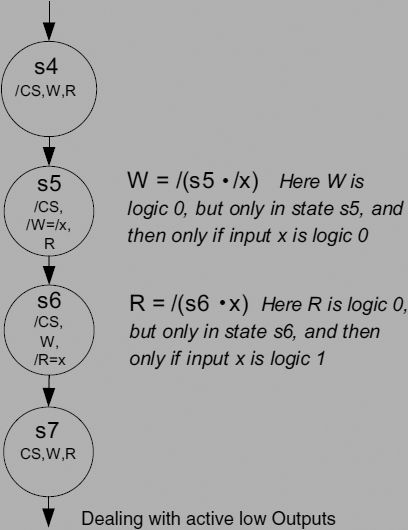
Figure 3.25 Dealing with active-low outputs.
In state s5, the output W is represented by
/W = /x.
This implies that, in state s5, W is to be logic 0, but only in state s5, and only if input x is logic 0.
When the equation for W is written, it also needs to contain the state s5 as
W = /(s5 · /x).
Note the whole of the right-hand side of the equation is inverted to provide the active-low output.
In a similar manner, in state s6 the output R is represented as
/R = x,
indicating that, in state s6, output R is written as to be logic 0, but only if input x is logic 1. The equation is
R = /(s6 · x).
Here, as with the W signal, the whole right-hand side of the equation is also inverted.
3.3 SUMMARY
This chapter has looked at the method of synthesizing a logic circuit from the state diagram. Methods have been developed to make this process simple and effective for implementation using both T-type flip-flops and D-type flip-flops. These methods are used in the development of further examples in Chapter 4.
At this point, the main techniques to be used in the development of synchronous design of FSMs have been completed and the rest of the book follows a more traditional format.
There is one more method to be considered in synchronous design, namely that of the ‘One Hot’ technique, which will be dealt with in Chapter 5.