
4
Synchronous Finite-State Machine Designs
This chapter looks at a number of practical designs using the techniques developed in Chapters 1 to 3. It compares the conventional design of FSMs with the design proposed in the book. This illustrates how more effective the latter method is in developing a given design. The traditional method of designing FSMs is common in a lot of textbooks on digital design. It makes use of transition tables and can become cumbersome to use when dealing with designs having a large number of inputs. Even for designs having few inputs, the method used in Chapters 1–3 is quicker and easier to use.
Most designers involved in the development of FSMs make use of unused secondary state assignments to help reduce the flip-flop input and output equations. This practice is investigated with some interesting results.
The chapter covers a number of practical system designs. Some have simulation waveforms showing the FSM design working. The Verilog HDL code used to create the simulations will not be shown, as Verilog HDL code development is not covered until later on in the book. However, the respective Verilog codes are available on the CDROM disk that is included with this book, as are the Verilog tools used to view the simulations.
Eight examples are discussed in this chapter, with each example introducing techniques that help to solve the particular requirements in the design being investigated.
4.1 TRADITIONAL STATE DIAGRAM SYNTHESIS METHOD
Before continuing with the development of FSM systems based on the synthesization method covered in Chapters 1–3, it is worth investigating the more popular traditional method of synthesization used by many system designers. Then see what solutions are obtained by using both methods. It should be possible to obtain the same results, or at least results that are of a similar level of complexity (i.e. number of gates).
Consider the state diagram shown in Figure 4.1. This, being a four-state diagram, will need two D-type flip-flops. Using the traditional synthesization method, begin by constructing a state table containing the present state (PS) values and the next state (NS) values for A and B, for all possible values of the input x. One then adds to this the next states for the inputs Da and Db, for all possible values of x. The result is the state table shown in Table 4.1.

Figure 4.1 A state diagram used in the comparison.
The values for A and B in Table 4.1 are obtained by inspection of the state diagram in Figure 4.1. For example, in state s0 (PS of AB = 00) in col1 the NS of AB for x = 0 will be 00 in col2; however, if x = 1, the NS of AB = 01 in col3 (i.e. s1).
The values for the NS Da and Db values will follow the NS values for AB because in a D flip flop the output of the flip flop (A, B) follows the Da and Db inputs.
The reader can follow the rest of the rows in Table 4.1 to complete the state table.
Table 4.1 Present state–next state table for the state machine.

The next step is to obtain the Da and Db equations from the state table by writing down the product terms where Da = 1 in both columns x = 0 and x = 1.
Consider, for example, Da = 1 when A changes 0 to 1; look for PS A = 0 to NS A = 1 in row 2, and PS A = 1 to NS A = 1 in row 3 of columns 1, 3 (x = 1):
- when PS AB = 01 (row 2) and x = 0, flip-flop A should set, and the product term /AB/x is required;
- when PS AB = 01 and x = 1 (row 2, col3), flip-flop A should be reset, and the term/ABx is not required;
- when PS AB = 10 (row 4) and x = 0, flip-flop A should set, and the term A/B/x is required;
- when PS AB = 11 (row 3) and x = 1, flip-flop A should be set, and term ABx is required.
Therefore, the D input terms for Da are
D·a = /AB·/x + A/B·/x + AB·x,
which cannot be reduced. For D·b = /A/B·x + /AB·/x + /AB·x + A/B·/x we have
D·b = /A·x + /AB + A/B·/x.
The output equation for Z = s3 = A/B, since this is a Moore state machine.
Now do the problem using the synthesization method described in Chapters 1–3.
From the state diagram directly:

This is the same as obtained using the traditional method.
The main advantage of the method used in Chapters 1–3, over the traditional method, is that it does not require the use of the state table. It is also much easier to use when the number of input variables is large (as is the case in large practical FSM designs) since the size of the present state–next state table increases as more inputs are added.
4.2 DEALING WITH UNUSED STATES
When developing state diagrams that use less than the 2n states for n secondary state variables the question of what to do with the unused states arises. Consider the state diagram of Figure 4.2.

Figure 4.2 A state diagram using less than the 23 states.
From the state assignment used in this example there are
| Used states | Unused states |
| s0 = 000 | s5 = 010 |
| s1 = 100 | s6 = 110 |
| s2 = 101 | s7 = 001 |
| s3 = 111 | |
| s4 = 011 |
The equations for D flip-flops are:

The crossed-out literals are a result of applying logical adjacency and the aux rule (see Appendix A). The result is

Again, the crossed-out terms are using logical adjacency and the aux rule.
C · d = A/B/C · x + AC · y + BC.
The output equations:

If the state machine falls into the unused state s5 (/AB/C) then the result will be
![]()
If the state machine falls into unused state s6 (AB/C):
![]()
If state machine falls into the unused state s7 (/A/BC):
![]()
This shows that the FSM designed with D-type flip-flops will be self-resetting.
Note that if T flip-flops are used, then the FSM will not be self-resetting since the T input either toggles with T = 1 or remains in its current state with T = 0. The only way to ensue that it does return to s0 is to make transitions available for this, as illustrated in Figure 4.3. Clearly, this requires more product terms in the equations for A · t, B · t, and C · t.
In general, if the state machine has a lot of 1-to-1 transitions and few 1-to-0 and 0-to-1 transitions, then T flip-flops may need less terms and, hence, a possible deduction in logic.
If the state machine has few 1-to-1 transitions the D flip-flop solution may result in fewer terms. However, the self-resetting features of the D flip-flop may provide a greater advantage in the overall design.
The rest of this chapter contains a number of practical examples, making use of the techniques developed in the first three chapters.
4.3 DEVELOPMENT OF A HIGH/LOW ALARM INDICATOR SYSTEM
Figure 4.4 illustrates a block diagram for the proposed system. In Figure 4.4, the FSM is used to control an ADC and monitor the converted analogue signal levels until either the low-level limit or the high-level limit is exceeded. The low- and high-level values are set up on the Lo-word/Hi-word inputs, which could be dual in-line switches. The comparators are standard 8-bit comparator circuits similar to the standard 7485 devices. These could easily be incorporated into a PLD/FPGA along with the FSM.

Figure 4.3 The arrangement needed for T flip-flops.
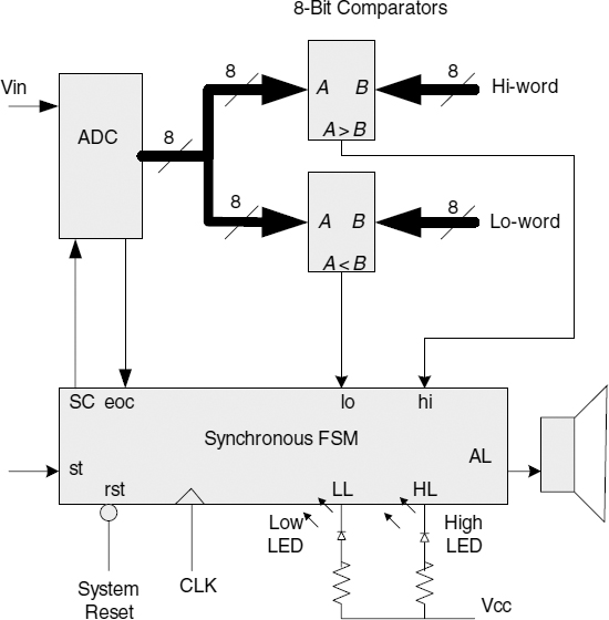
Figure 4.4 Block diagram for the High/Low detector system.
In this application it is assumed that, when the ADC output A exceeds the Hi-word, hi will go to logic 1. An ADC output less than the Lo-word will make lo go to logic 1. The ADC could be a separate device or its digital circuits could be implemented on a PLD/FPGA device and an external R/2R network connected to the chip.
The system is to start when st goes high. It should perform analogue-to-digital conversions at a regular sampling frequency dictated by the system clock and when either the Hi-word or Lo-word are exceeded, turn on the appropriate LED indicator and stop. It can be returned to its initial state by operation of the reset button. Note that in this example the alarm will not sound for an ADC output that is equal either to Hi-word or Lo-word.
From this specification, a state diagram can be developed. The control of the ADC will follow in much the same way that was used in Chapter 2.
The two digital comparators being combinational logic will give an output dependent on the level of the ADC output. When the ADC output is equal to or less than hi-word but greater than Lo-word, then both lo and hi will be low, signifying that the ADC value is between the two limits. When the ADC output is greater than Hi-word, then hi will be logic 1 and is to sound the alarm and turn on the HL indicator. When the ADC output is less than Lo-word, then lo becomes logic 1 and the alarm turns on the LL indicator.
A state diagram has been developed as shown in Figure 4.5. Looking at this state diagram, the system sits in s0 from power on reset and waits for the start input to go high. Then the ADC signal SC is raised to perform an analogue-to-digital conversion. After this the system falls into s2. Here, the outputs from the two comparators are checked, and if either the Hi-word or the Lo-word limit has been exceeded then the state machine will fall into s3. If, however, neither limit has been exceeded, then the state machine will fall back into s1 to perform another analogue-to-digital conversion.

Figure 4.5 A possible state diagram for the problem.
Looking at the two-way branch state s2, it is clear that the inverse of lo + hi is /(lo + hi). As an aside, if one applies De Morgan's rule to /(lo + hi) one gets /lo · /hi, indicating for the transition from s2 to s1 that both lo and hi must be low.
Moving on to look at s3, one can see that the two outputs HL and LL are dictated by the logic state of the comparator outputs lo and hi so that in s3 the HL indicator should be active if hi = 1, whereas the LL indicator should be active if lo = 1.
/HL = hi in s3 indicates that HL must be active low. The output equation for HL will be written as
HL = /(s3 · hi),
which means that HL will be logic 0 when hi = 1, but only when the state machine is in s3. This is defining a Mealy active low output. This is how it was defined in Chapter 3.
In a similar way, LL = / (s3 · lo).
The best way to remember this idea is to think of the /HL = hi equation in the s3 state as representing the equation HL = /(s3 · hi), but then written inside the state circle one does not need to include the s3, as it is implied.
Replacing the state number s3 with its secondary state variable value AB = 01, the two Mealy outputs can be written as
![]()
which results in two three-input NAND gates. Remember, active low signals are inverted (see Chapter 3).
So, from the equation for HL = /(/A · B · hi) it can be seen that, when in state s3, A = 0 (/A = 1), B = 1, and if hi = 1 then the output of the NAND gate will be zero, which is exactly what is required to light the LED indicator (active low output).
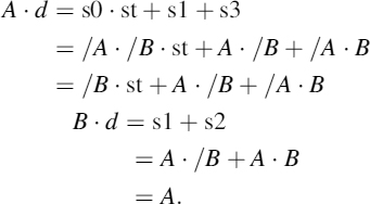
Having gone into some detail to describe the logic behind the Mealy outputs, the next step is to determine the equations for the two flip-flops A and B. Using the method described in Chapter 3 for D flip-flops, these are
A · d = s0 · st + s1 + s2 · /(lo + hi) = /A · /B · st + A · /B + A · B · /hi · /lo.
The equation for A · d could be simplified using the Auxiliary rule to form
A · d = /B · st + A · /B + A · /lo · /hi.
Moving on to flip-flop B:
B · d = s1 · eoc + s2 · (lo + hi) + s3. = A · /B · eoc + A · B · lo + A · B · hi + /A · B.
Again, using the Auxiliary rule:
B · d = A · /B · eoc + B · lo + B · hi + /A · B.
The remaining Moore-type outputs are SC = s1 = A · /B and AL = s3 = /AB.
The next stage would be to develop a Verilog HDL file describing the circuit for the FSM, and comparators. This has been done and is contained on the CDROM in the Chapter 4 folder.
4.3.1 Testing the Finite-State Machine using a Test-Bench Module
In this simulation (Figure 4.6), a test-bench module is added to the Verilog code in order to test the FSM. To do this, test all paths of the state diagram. In the simulation of Figure 4.6 this has been achieved by first following the path s0 → s1 → s2 → s3 with a low limit exceeded and the FSM remains in s3 (A = 0, B = 1) until a reset (rst = 0) is applied. Then, the sequence is repeated with a Hi limit exceeded, followed by another reset. Finally, the sequence s0 → s1 → s2 → s1 → s2 → s1 → s2 → s1 → s2 → s0 is followed, representing a no limits exceeded until finally another rst = 0 resets the FSM back to s0. Thus, in this way the FSM is tested.

Figure 4.6 Simulation of the FSM controller.
4.4 SIMPLE WAVEFORM GENERATOR
Sometimes there is a need to generate a waveform to order, perhaps to test a product on an assembly line. An oscillator could be used for this purpose, but it can be tedious to build an oscillator to do this if the waveform is not a pure sine wave, square wave, ramp, or triangular. One way of generating a complex waveform would be to use a microcontroller with a digital-to-analogue converter (DAC). The complex waveform could be stored into read only memory (ROM) and accessed via the microcontroller. However, this seems overkill. There are also potential sampling frequency limitations with the microcontroller. An alternative way would be to use a clocked FSM. The sampling rate could then be controlled by the clockrate, which would be limited by that of a PLD or FPGA. The complex waveform is still stored in a ROM but the ROM is controlled by the FSM.
Consider the block diagram of Figure 4.7. In this system, raising the st input starts the waveform generator. Each memory location is accessed in sequence and its content, a digitized sample of the waveform, is sent to the DAC to be converted to an analogue form. When the end of memory is reached, the address counter simply runs over to the zero location and starts again.
Setting the st input low stops the system. The actual sampling rate and, hence, the period of the waveform can be calculated once the state diagram is completed. The output of the DAC will need to be filtered to remove the sampling frequency component – this can be accomplished using a simple first-order low-pass filter section if the sampling frequency is much higher than the highest synthesized waveform frequency. (Usually, it is to satisfy Shannon's sampling theory.)
The state diagram now needs to be developed. A little thought reveals that the block diagram itself provides an indication of the sequence required.

Figure 4.7 Block diagram for simple waveform generator.
- Initially, the address counter needs to be cleared to provide the necessary zero address for the first location of the memory. The system should remain in state s0 until the start input st is asserted (high).
- The memory then needs to be enabled, selected, and allowed to settle, after which the data in the memory location will be available at the data latch inputs. Then the data need to be latched into the data latch to be available at the input of the DAC.
- At this stage, the address counter needs to be incremented so as to point to the next memory location and the sequence in 2 repeated again as long as the start input is still asserted (high).
Note that, in this problem, the end of memory location is not an issue, since the address counter can be allowed to overrun and start from location zero again. This does imply that the waveform information can be fitted into the memory device so that the waveform is produced seamlessly. It would be possible to add further logic to the system to ensure that this was always the case, but this is not done in this example.
The state diagram can now be developed following the sequence of activities described above.
In Figure 4.8, the state diagram is seen to follow the sequential requirements for the system. Note that in s3 the P output is a Mealy output. P is gated with the clock and can only go high when in s3, and then only when the clock is low. This ensures that the address counter is pulsed (on the rising edge of P) after the memory enable EN is disasserted (high). Therefore, the memory data outputs will be tri-state during the change of memory address. The Data Latch ensures that the DAC always has a valid data sample at its input. Note that an alternative arrangement for output P would be to provide an additional state between s3 and s1 in which P = 1. This would avoid the potential for a glitch at P output (as discussed in Chapter 1).
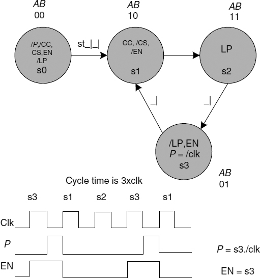
Figure 4.8 The complete state diagram for a simple waveform generator.
The equations can now be developed:
Outputs are

In Verilog, these equations can be entered directly, but using the Verilog convention for logic:
![]()
These equations would be contained in an assign block thus:
assign
A. d = ~ B& st|A&~B|~A& B,
B.d = A,
CC = ~ (~ A & ~ B);
CS = ~ A& ~ B,
LP = A&B,
EN = ~ A,
P = ~ A&B&~ clk;
Appendix C contains a tutorial on how to produce a Verilog file to simulate a state machine. Also, much more detail is available in Chapters 6 to 8.
4.4.1 Sampling Frequency and Samples per Waveform
From the state diagram of Figure 4.8 it is apparent that the system cycles though three states for every memory access, so the sampling period is three times the clock period.
Therefore, for a sampling frequency of 300 × 103 Hz, a clock of 300×103×3 = 900×103 Hz is required. For a critical sampling-rate application, a dummy state could be added to make the sampling frequency four times the clock frequency (for example).
The size of the memory can be whatever is required for the systems use, and will dictate the size of the address counter. If the memory is 1 Kbyte, the address counter needs to be
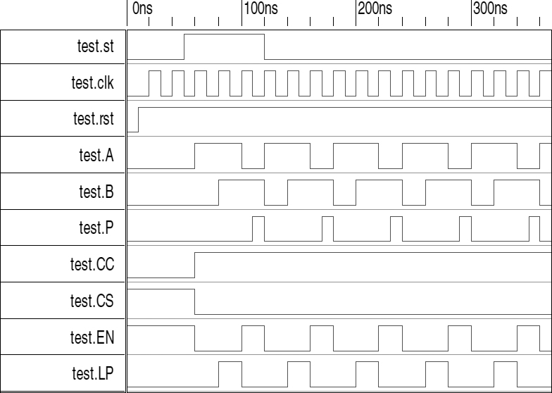
Figure 4.9 Simulation results for the FSM of the waveform synthesizer.
Number of flip-flops in address counter = ln(1024)/ln(2) = 10.
The simulation of the FSM is illustrated in Figure 4.9.
4.5 THE DICE GAME
In this example the system consists of seven LED indicators, a p input, and a clock. The block diagram of the system is shown in Figure 4.10, with a single push switch p. The clock input could be a simple oscillator circuit using a 555 timer chip running at 100 Hz so as to provide a flicker to add effect.
The LED indicators are arranged as illustrated in Figure 4.11 to look more realistic. In this design it is assumed that low-current LEDs are used with a forward current of 2 mA. This makes the current-limiting resistors 1800Ω for a 5 V supply. It is also assumed that the FSM outputs are open drain. Figure 4.11 illustrates how the seven LED indicators would look for each number displayed. The situation when all LEDs are off is not shown.
The state machine is simple to develop, as all that is required is to display each number in sequence, but at a speed that the user cannot follow. The state diagram consists of seven states, each one to display a given LED pattern. The transition between each state is conditional on the input p being equal to one for each transition. When the user releases the p button the FSM will stop in a state. Because of the frequency of the clock, the user will not be able to follow the state sequence, thus realizing the chance element of the game. Note that if the clock frequency is too high then all the LED indicators will appear to be on when the p button is pressed. Having a slower clock frequency leads to a flicker effect and, thus, adds to the excitement of the game. Figure 4.12 shows the state diagram for the system.
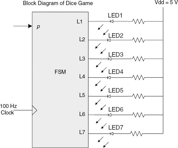
Figure 4.10 Block diagram of the dice game FSM
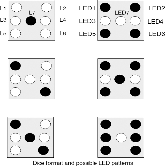
Figure 4.11 Dice format for numbers.
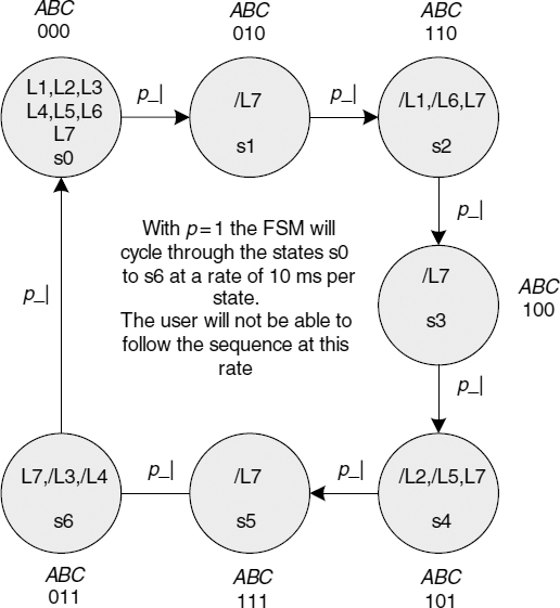
Figure 4.12 State diagram for the dice game.
4.5.1 Development of the Equations for the Dice Game

This can be reduced to
which reduces to
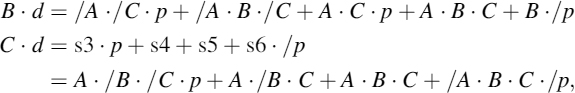
C · d = A · /B · p + B · C · /p + A · C.
The outputs (LEDs are active low) are

Figure 4.13 illustrates the dice FSM running through each state. The secondary state variables a, b, and c can be seen to be moving through each state. The outputs L1 to L7 are responding as expected and are illustrated in Figure 4.11.
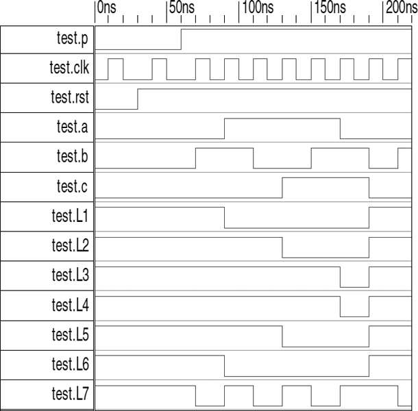
Figure 4.13 Simulation of the dice game.

Figure 4.14 Dice game simulation with p input released showing FSM stopped in s3.
In Figure 4.14, the input p has been simulated as ‘on’ then ‘off’. The FSM is seen to have stopped in state s3, then started again when p is set to logic 1.
Note that in both simulations the time-scale is in nanoseconds, but in practice the clock would be slowed down to a 10 ms period.
4.6 BINARY DATA SERIAL TRANSMITTER
The next example involves sending the 4-bit binary codes of a counter to a shift register to be serially shifted out over a serial transmission line.
Figure 4.15 shows the block diagram for a possible system. The FSM is used to control the operation of the Binary Counter and the Parallel Loading Shift Register. Both of these devices could be designed using the techniques described in Appendix B on counting methods. This leads to a Verilog description (module) for each device.
The system is started by raising the st input to logic 1. This is to cause the FSM to remove the reset from the Binary Counter and then load the current count value of the counter into the parallel inputs of the shift register. On releasing the parallel load input LD to logic 1, the shift register will clock the count value out over its transmit output (TX) at the baud rate dictated by the clock. When the shift register is empty its RE signal will go high and this will be seen by the FSM, which will then determine whether the last count value has been sent. This is seen by the FSM when done = 1, detected by the detector block (an AND gate). If not the last counter value, then the next count value will be loaded into the shift register and the sequence repeated until all count values have been sent. At this point the system will stop and wait for st to be returned to its inactive state before returning the FSM to its s0 state.
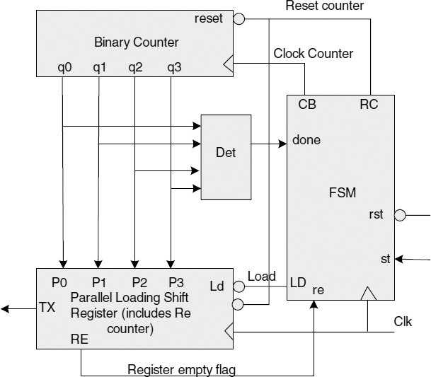
Figure 4.15 Block diagram of the binary data serial transmitter.
From the above description, the state diagram in Figure 4.16 is developed. This state diagram is correct, but it is difficult to obtain a unit distance code for the secondary state variables. If a dummy state s7 is added, then a unit distance coding between s6 and s0 can be obtained for the secondary state variables A, B, and C. Note: it is not apparent from Figure 4.17, but the outputs in state s7 are the same as the state it is going to (s0), apart from the RC output. The s5 to s1 transition is not unit distance. If glitches are produced in any outputs, then dummy states could be introduced between s5 and s1 to establish unit distance coding. The reader might like to try to establish a unit distance code for the state diagram. This would require introducing an additional state variable (flip-flop), since all 23 states have been used in this design.
Using Figure 4.17, the equations for the FSM are obtained from the state diagram and implemented using D flip-flops:

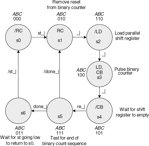
Figure 4.16 State diagram for the binary data serial transmitter.

Figure 4.17 State diagram with additional dummy state s7 to obtain unit distance code for the secondary state variables.

reducing to
B · d = /A · /C · st + /A · B · /C + A · C · re + B · C · st + A · B · C
C · d = s3+s4+s5 · done + s6 = A · /B · /C + A · /B · C + A · B · C · done + /A · B · C,
reducing to
C · d = A · /B + B · C · done + /A · B · C.
The outputs (all Moore) are

The serial transmitter simulation is shown in Figure 4.18. The state machine is tracked through its state sequence in the usual way by comparing the A, B, and C values in Figure 4.18 with the state diagram A, B, and C values in Figure 4.17.

Figure 4.18 Simulation of the binary data serial transmitter.
4.6.1 The RE Counter Block in the Shift Register of Figure 4.15
The shift register in Figure 4.15 has an output RE to flag the point at which the register is empty. This can easily be obtained by using a four-stage Binary Counter that becomes enabled when the load input is disasserted (high). The counter can then be clocked with the same clock as the shift register; then, when it reaches its maximum count 1000, the most significant bit is used as the RE signal. Table 4.2 illustrates the effect.
From Table 4.2 it can be seen that when the counter reaches the eighth clock pulse the counter rolls over to set the most significant bit of the counter D to logic 1. This bit acts as the RE register empty bit. After shifting out the binary number, the FSM will return to its s0 state, where the RC output will once again go low and reset both the Binary Counter and the RE counter in the shift register. Note that in this particular design an additional flip-flop E could be added to the binary counter and this used as the RE output instead
The equations to describe the RE counter can be developed from the material in Appendix B on counting applications. The equations, using T-type flip-flops, are

This last example has illustrated how a complete design can be developed in terms of Boolean equations that can be directly implemented in Verilog HDL (or any other HDL for that matter).
There are examples in Appendix B showing how a synchronous binary counter can be implemented using T flip-flops. Of course, the counter could be implemented as an asynchronous (ripple-through) counter if desired.
Table 4.2 Illustrating the effect of a binary counter used to determine shift register empty.

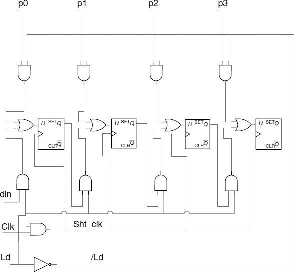
Figure 4.19 The 4-bit parallel loading shift register from Equations (B.9) to (B.12).
Also in Appendix B is an example of a parallel loading shift register using D flip-flops. The equations for a four-stage shift register are repeated below from Appendix B:
Figure 4.19 shows the schematic circuit for the 4-bit parallel loading shift register developed from Equations (B.7)–(B.11).
4.7 DEVELOPMENT OF A SERIAL ASYNCHRONOUS RECEIVER
Often, there is a requirement to use serial transmission and receiving of data in a digital system. Although there are lots of serial devices on the market, it is useful to be able to implement one's own design directly to incorporate into an FPGA device. The advantage of this approach is that the baud rate and protocols can be dictated by the designer, as can how the device will be controlled.
In this example, the serial data input is encapsulated into an asynchronous data packet with start (st) and stop (sp) protocol bits that have been added to the serial transmission packet. These are used to provide a means of identifying the data packets as they arrive. This allows the data packets to arrive at any time and at any selected rate (dictated by the baud rate).

Figure 4.20 Protocol of the serial asynchronous receiver.
The problem with receiving data is that it is necessary to ensure that the shift register is clocked with correct data bits. To do this the FSM clock is used to drive an FSM to create a shift register clock RXCK in the middle of the data bit time period. This RXCK clock pulse can be seen in Figure 4.20 as the arrowed pulses occurring every third clk pulse. Thus, the clk signal runs four times faster than the RXCK signal generated by the FSM. Note, the FSM needs to detect the start of the data packet by looking for the 1-to-0 transition on the receiver input.
The block diagram for the serial asynchronous receiver is illustrated in Figure 4.21. The FSM is used to create the shift register clock, and to control the operation of the serial asynchronous receiver. The Divide by 11 Counter is used to count out the 11 bits that make up the protocol packet. This provides a shift register full signal rxf to indicate to the FSM that a complete data packet has arrived. The Data Latch is used for collecting the received data from the shift register to send to the outside world device controlling the asynchronous receiver.
The FSM must wait for start (by monitoring for the st bit change 1 to 0); this is just the first receive bit coming into the shift register. When detected, shift the data into the shift register. If the stop bit is not correct, then the FSM can issue an error via signal ERR. Note, in this version the start bit is tested along with the two stop bits via an AND gate (error detection signaled) to ensure packet alignment after the complete packet is received, the receiver rx input is held at logic 1 by a pull-up resistor so that the start bit (active low) can be detected. The ack signal is available so that the outside world device using the system can respond to an error condition (no error means successful packet received). Healthy data packets will be latched into the data latch ready to be read by the controlling device.
The signal CDC is used to clear the shift register and set st to logic 1, i.e. the flip-flop representing the start bit of the shift register needs to be pre-set so that it can be cleared by the incoming start bit from the serial line.

Figure 4.21 Block diagram of the serial asynchronous receiver.
The en signal is used to enable and start the asynchronous receiver. This is necessary to ensure that the system starts monitoring the clock so as to issue the shift register clock pulse (RXCK) at the right time (in the middle of the data bit period).
Figure 4.22 illustrates the state diagram for the system. In Figure 4.22, the FSM waits for the enable signal en going high and start signal st going low; it then moves through states s1, s2, and s4 and onto s5 to shift the start bit into the shift register. This is required in order to ensure that the start bit is detected and then shifted at the right time. In state s5, the shift register clock RXCK is pulsed to place the start bit into the shift register. It then falls into state s6, sending RXCK low and proceeds to cycle through the second loop consisting of states s5, s6, s7, and s8.
These states count out the clock cycles and produce a shift register clock pulse (RXCK) at the right time near the middle of each data bit. After all 11 bits have been clocked into the shift register the 11-bit counter will issue a receive register full signal rxf, and the FSM will now fall into state s9, where the start and stop bits are tested (ed should be logic 1). If ed = 0, then the FSM will move into s10 and issue the error signal.
The controlling device can then reset the asynchronous receiver and start again. If no error, then the FSM moves to s11 to latch the data in the shift register into the data latch ready for the controlling device to read (OQ0 to OQ7). It will also issue a data ready signal (DRY) to the controlling device, which will acknowledge this by raising an ack signal. The FSM can then move back to s0 via s12 (when ack goes low) to wait for the next data packet. The DRY and ack signals form a handshake mechanism between the FSM and the controlling device.

Figure 4.22 State diagrams for the serial asynchronous receiver.
The device enable signal en will be left high until all data packets have been received.
Note that the state assignments miss s3, which was removed from the state diagram during development when state s3 was no longer needed (owing to an error in the design at that time). State diagram development tends to be an iterative process.
4.7.1 Finite-State Machine Equations

The reader may like to complete these to form the equations in terms of A, B, C, and D.
The complete asynchronous serial receiver block is simulated, together with all the modules in Figure 4.21, in Appendix B.
4.8 ADDING PARITY DETECTION TO THE SERIAL RECEIVER SYSTEM
The foregoing example could be improved upon by making the first stop bit sp1 into a parity bit. The parity bit would require combinational logic to check each bit of the protocol packet for either even parity or odd parity. This would require an exclusive OR block made up of the 11 bits of the packet.
For example, odd parity would require an odd parity output OP at the Transmitter of
OP = bo^b1^b2^b3^b4^b5^b6^b7^b8^b9^b10.
Or, including the protocol bits:
OPn+1 = st^d0^d1^d2^d3^d4^d5^d6^d7^OPn ^sp.
This output would be tested by the FSM for logic 1. If logic 0, this would indicate that one or more of the received bits was faulty.
Note that even parity EP can be detected by complementing the OP signal:
EPn = /OPn.
To implement the parity detector term, two input exclusive OR gates are cascaded with the last exclusive OR gate providing the OPn signal. The output of the parity block at the receiver is P.
The inputs d0, d1,…, d7 will be obtained from the output of the shift register in each case (see Figure 4.21).
4.8.1 To Incorporate the Parity
The parity detector inputs are connected to the outputs of the shift register and its output OPn made available as an input to the FSM via the last two bit comparator comparing OPn and OPn+1 in Figure 4.23.
Figure 4.24 shows the new protocol with the parity bit OPn (shown in lower case) replacing sp1.
Figure 4.25 shows the additional parity block added to the block diagram. This version detects stop and parity bit errors at the output of the shift register; the start bit has not been tested (but could be included if desired).
Figure 4.26 illustrates the modified state diagram with ODD parity detection. Note that the input parity bit OPn+1 must be compared with the generated parity bit OPn. If both are the same, then there is no parity error. This comparison can be made with a 2-bit exclusive NOR gate having an output P (OPn == OPn+1) being logic 1 if there is no parity error and logic 0 otherwise. This output is an input p to the state machine (see Figure 4.25).
In state s9, the bit sp is checked to find out whether the whole packet has been input, and s11 now tests for an odd parity error. In either case a failure will result in the FSM aborting the receive packet process and falling into state s10 to await a reset from the controlling device. The logic used in Figure 4.21 could be used to detect for start and stop bits if desired.

Figure 4.23 Arrangement of the parity generation and detection logic.
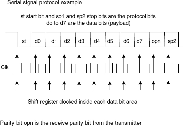
Figure 4.24 Protocol with parity detection bit added.
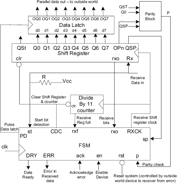
Figure 4.25 Block diagram with parity block added.
4.8.2 D-Type Equations for Figure 4.26
In the following equations, the variable P is the output of the parity check (OPn = OPn+1) connected to the input p of the FSM. See Figure 4.23.

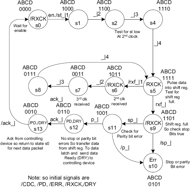
Figure 4.26 The state diagram with odd parity added to FSM.
The outputs are as they were in the state diagram of Figure 4.22, except for

The FSM part can be simulated, and this is illustrated in Figure 4.27. In this simulation, the test sequence is
s0, s1, s2, s4, s5, s6, s7, s8, s5, s9, s11, s12, s13, s0, s1, s2, s4, s5, s9, s10, s0, s1, s2, s4, s5, s9, s11, s10.
This ensures that all paths of the state diagram have been tested.
This should now be followed by a series of tests of all the other components, i.e. the shift register, the divide-by-11 counter, and the parity block, before going on to test the whole system.
4.9 AN ASYNCHRONOUS SERIAL TRANSMITTER SYSTEM
Having developed an asynchronous receiver module, an asynchronous transmitter is required to complete the serial device. Figure 4.28 shows the block diagram for an asynchronous serial transmitter.

Figure 4.27 Simulation of the FSM for the serial receiver.
In Figure 4.28, the input Data Latch provides the data to be transmitted and the protocol bits st and sp are set to their expected values before being loaded into the Shift Register via the LD output from the FSM. Note that there is no need for a slower transmit clock, as the FSM can provide the shift register pulse at the right time.
The sequence is started by data being presented onto the parallel data inputs then the send input being sent high by the controlling device. The FSM then loads the data into the shift register and starts transmitting it out to line. The Divide by 11 Counter records the point at which the packet has been sent to line by raising the Transmit Register Empty (txe) signal high. The FSM can then send a Request To Send (RTS) signal to the controlling device to inform it that the data packet has been sent. The controlling device can set the ack signal high to say it has acknowledged this operation.
A possible solution is illustrated in Figure 4.29.
It is important to ensure that the clock signal to the shift register is the same frequency as the one used in the asynchronous receiver block. If it is not, then the receiver will not be able to receive the data packets. Even if the two clocks are different by only a small amount, a frame error could arise. This is when the difference in clock speeds produces a small difference in the total packet time and, hence, one or more data bits can be lost. In effect, start and stop bits must be sent and received correctly.

Figure 4.28 Block diagram for an asynchronous serial transmitter.
Total packet time = 11 × 1/(clock frequency).
For example, if the transmitter shift register clock is 1 MHz (usually referred to as the baud rate), then
Total packet time = 11 × 1/(1 × 106) = 11 × 1 μs = 11 μs in duration.
The receiver shift register clock does have a tolerance; this is a result of the fact that the data are sampled within a four-clock window (see Figure 4.20) and a small difference in the two packet lengths can be accommodated.
In some commercial Universal Asynchronous Receiver Transmitter (UART) devices, 16 (rather than 4) is used for the clk signal used to generate the shift register clock (RXCK), giving a greater resolution for detecting the logic value of the data bits.
Generally, if the clocks in both the transmitter and the receiver are of a high accuracy (as one would expect from crystal oscillators), then there is usually not a problem. It would be easy to restructure the receiver state diagrams of Figures 4.22 and 4.26 to accommodate a higher resolution shift register clock by adding more states in the loop comprising s5 to s8, and adding states between s1 to s5 for the start bit. However, such a design could make use of the One Hot method covered in Chapter 5.
Note that the FSM clock is four times that of the baud rate.
The state diagram for the asynchronous transmitter is illustrated in Figure 4.29. In this state diagram, the shift register is clocked every four FSM clock pulses as it moves between s4, s8, s9, and s5. Note that for a 1 μs baud rate the transmitter FSM clock would need to be 4 MHz.
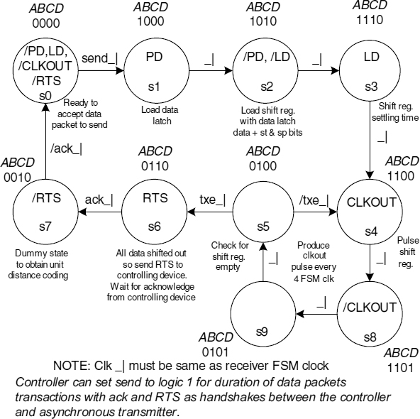
Figure 4.29 State diagram for the asynchronous serial transmitter.
4.9.1 Equations for the Asynchronous Serial Transmitter

A simulation of the FSM results in the waveforms of Figure 4.30. In this simulation, the test sequence is s0, s1, s2, s3, s4, s8, s9, s5, s4, s8, s9, s5, s6, s7, s0.
Using the asynchronous transmitter and receiver FSMs just described, it would be possible with modern FPGAs to run at quite high baud rates, as illustrated below.

Both transmit and receiver units use the same FSM clock frequency generated with their own clock circuits.
The higher baud rates would need to use twisted-pair cables over relatively short transmission distances up to around 1 m. Transmission line effects would need to be taken into account, but this is beyond the scope of this book.

Figure 4.30 Simulation of the serial transmitter FSM.
4.10 CLOCKED WATCHDOG TIMER
Most microcontrollers these days have a builtin watchdog timer (WDT). The WDT is an addressable device that can be written to on a regular basis. The idea is that the timer (usually a down counter) is regularly written to reinitialize it to a known count value. Between writes, the counter will be clocked towards zero. If the microcontroller does not write to the WDT between countdown periods, then the counter will reset to zero and this action can be used to reset the microcontroller.
The WDT thus acts as a safeguard to prevent the microcontroller from running out of control (jumping to an instruction that is not part of the program sequence), perhaps due to a transient in the power system.
Another use is in a microprocessor-based system where the operating system (perhaps a real-time operating system) can regularly reset the WDT and, hence, provide a means of determining a microprocessor system failure.
The application program running on the microcontroller needs to write regularly to the WDT to prevent it from reaching the reset state.
Although most microcontrollers have this feature, a lot of microprocessor systems do not. Therefore, a circuit would need to be designed for this purpose.
The clocked FSM system shown in Figure 4.31 is a basic system designed to perform the action of a WDT. The system needs to be designed around the specific memory/IO cycle timing of the microprocessor. In Figure 4.31 the memory/IO write cycle is based around a four-clock pulse cycle time T1 to T4.

Figure 4.31 Block diagram for a WDT for a microprocessor system.
The system is controlled by an FSM that monitors the chip enable ce controlled by the address decoding logic. This can respond to a particular address from the microprocessor. In addition, the iow signal controlled by the microprocessor is also monitored by the FSM. When the microprocessor addresses the WDT, ce goes low, followed by iow in the T2 clock period. On the rising edge of the T3 clock period, the WDT pulse is generated. The FSM must produce this watchdog pulse (WDP) at exactly the right time in the write cycle (T3 period). Both the FSM and the down counter are clocked by the same microprocessor clock clk.
In Appendix B, the design of a down binary counter is described and Section B.1 shows how this can be done. To provide this counter with a fixed starting value (to count down from), the flip flips of the counter can be preset to a known value, using a parallel loading counter (see Section B.3). This is the purpose of the initialize input in Figure 4.31 (essentially a parallel load input to the down counter).
Note that this same input provides the initial state for the FSM (which will be state zero). The WDP will provide frequent reinitialization pulses to the down counter and, thus, prevent it from reaching its zero state (which would otherwise cause a microprocessor reset).
A suitable state diagram is illustrated in Figure 4.32, wherein the FSM waits in state s0 for the microprocessor to write to the address of the WDT. This will cause ce to go low during the T1 state of the memory/IO cycle (see Figure 4.31) so that on the T2 rising clock edge the FSM will move into s1. Here, it waits for the microprocessor to lower iow; then, on the next clock pulse (T3), the FSM will move into state s2, where it will lower the WDP output signal. On the next clock pulse (T4), the FSM will move to s3, raising the WDP, and wait for the ce signal to go high. This will occur at the end of the memory/IO write cycle and will be seen by the FSM on the rising edge of T1.
The equations for the FSM that follow are from Figure 4.32.
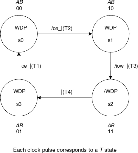
Figure 4.32 State diagram for the WDT.
4.10.1 D Flip-Flop Equations

4.10.2 Output Equation
WDP = /(s2) = /(A · B).
The equation for ce would depend upon the desired address assigned to the WDT. For example, if the address assigned was 300h (11 0000 0000 binary), then the equation would result in
ce = /(a9 · a8 · /a7 · /a6 · /a5 · /a4 · /a3 · /a2 · /a1 · /a0).

Figure 4.33 The WDT FSM simulation.
There could be additional qualifier signals, i.e. in a PC using the IO memory map the signal /aen would be required in order to distinguish between dynamic memory access (DMA) cycles and IO cycles (see Chapter 5 for DMA). Also, the /iow signal would be needed to identify a write cycle.
The above equation for ce would then be
ce = /(a9 · a8 · /a7 · /a6 · /a5 · /a4 · /a3 · /a2 · /a1 · /a0 · /aen · /iow).
The equations to describe the down counter are repeated below from Appendix B for convenience.
![]()
This equation expands to

for a four-stage down counter.
Note that the counter needs an asynchronous initialization signal connected to each T flip-flop to form the parallel loading input logic (see Equation (B.4) and Figure B.4).
Figure 4.33 shows the FSM in action. The output WDP goes low during state s2 after the address-decoding ce and iow have been detected going low in sequence. The FSM state transitions are clearly seen in the flip-flop A and B outputs.
Note that in the above simulation there are additional clock pulses. These have been generated by the test bench generator to test for the FSM remaining in states s0 and s1 until changes in the ce and iow signals occur. This would not happen in practice, since the microprocessor has control of iow and the address-decoding logic ce.
4.11 SUMMARY
In this chapter, a number of practical examples have been developed using the block diagram and state diagram approach developed in the Chapters 1–3. These have then been implemented in terms of D-type flip-flops. You may well decide to use some of these examples in your own designs, or expand upon them to make them fit your own requirements.
In the next chapter, the idea of having a state for each D-type flip-flop will be introduced, leading to systems that do not need secondary state variables.