
5
The One Hot Technique in Finite-State Machine Design
5.1 THE ONE HOT TECHNIQUE
The FSMs designed up to now have used secondary state variables to identify each state. This requires the use of unit distance assignment, where possible, to try to avoid potential glitches in output signals.
An alternative would be to assign a flip-flop for each state. Although this may be considered wasteful, it has the advantage that it would in theory avoid the generation of output glitches, since each state would have its own flip-flop. At any one time, only one flip-flop would be set, i.e. the one corresponding to the state the FSM was currently in.
This idea is called ‘One Hotting’ and is much used in FSM designs that are targeted to FPGAs. This is because FPGAs have an architecture that consists of many cells that can be programmed to be flip-flops, or gates. So a large number of flip-flops is not difficult to achieve. A PLD, on the other hand, has an architecture with only a limited number of flip-flops controlled from AND/OR ‘sum of product’ terms.
Another feature of the One Hot technique is that it can require fewer logic levels because there is no required logic from other state variables apart from the primary inputs and previous state(s). This can result in faster logic speeds.
The method of implementing a ‘One Hot’ FSM will now be described.
Consider Figure 5.1. In this example of the use of the One Hot technique, the single-pulse generator with memory problem is revisited. It uses three states (rather than the four-state FSM used in the original design). This is possible because one does not have to consider unit distance coding and, hence, there are no secondary state variables.
The equations on the right in Figure 5.1 are the equations necessary to synthesize the FSM. To understand where these come from, consider the One Hot state diagram.
Initially, the FSM should be in state s0. This can be arranged via an initialization input so that the flip-flop representing state s0 (called FFS0) is set, and all other flip-flops (FFS1 and FFS2) are reset.

Figure 5.1 An example of the use of the One Hot technique.
Consider state s0. Here, the FSM should remain in state s0 until the condition to exit s0 occurs. This is, of course, when the primary input signal s becomes logic 1.
However, the flip-flop FFS0 needs a signal on its D input that will keep it in the set state. The required signal is
s0 · /s.
This is obtained from the fact that the FSM is in state s0 and the ‘leaving condition’ from state s0 is s, so that while s is not true, i.e. s = 0, or /s, the flip-flop should remain set.
This term s0 · /s is known as a ‘hold term’ because it holds the FFS0 set until it is required to change to the next state, s1.
Also, when the FSM reaches state s2 it will only return to state s0 when the signal s is logic 0. So there is another term:
s2 · /s.
This is known as the ‘set term’, or ‘turn on’ term, for the flip-flop.
The complete equation for the state s0 flip-flop FFS0 is
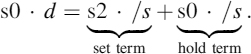
Now consider state s1. The condition to enter state s1 is when the FSM is in state s0 and s = 1. So, the equation for flip-flop FFS1 is
s1 · d = s0 · s.
Note that the ‘leaving condition’ from s1 is a simple clock pulse. There is no input condition along the transitional line between s1 and s2; therefore, when the FSM reaches state s1, it will naturally exit state s1 on the next clock pulse, so a ‘hold term’ is not needed.
Now consider the final state s2.
The condition to enter state s2 is s1, since there is no input condition along the transitional line between states s1 and s2. There will, however, be a holding term between s2 and s0, which is
s2 · s.
While s = 1 the FSM must remain in state s2. So the equation for FFS2 will be
s2 · d = s1 + s2 · s.
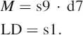
Finally, the output signal is
P = s1,
since only in state s1 will the output P be logic 1; L will only be active in state s2:
L = s2.
The circuit for this FSM is illustrated in Figure 5.2. Note in Figure 5.2 the initialization logic is fitted retrospectively. In a One Hot system, one of the flip-flops, representing the initial state in the FSM, needs to be set, while all other flip-flops need to be cleared. If flip-flops without preset and clear inputs are used, then a synchronous reset scheme needs to be adopted (as seen in Chapter 3, Frames 3.16 and 3.19).
Figure 5.2 Circuit for the One Hot version of the single-pulse FSM.

Figure 5.3 A second example with two-way branch.
Now consider the two-way branch FSM design in Figure 5.3. In this example, the equation for FFS0 follows the rules already explained for the first example. In the equation for FFS1, however, note that there is a term for entering state s1 via s0 (s0 · st) and a term to enter via s3.
The two-way branch leaving state s1 is via s1 · x(to state s2) and s1 · /x (to state s3), and the combined terms result in
s1 · d = s0 · st + s3 + s1 · x · /x,
which reduces to
s1 · d = s0 · st + s3
because the s1 · x · /x terms would reduce to zero:
s1(/x · x) = 0.
The FSM is held in s1 by complementing the inputs such that the leaving term between s1 and s2 (x) is complemented (/x) and the leaving term between s1 and s3 (/x) is also complemented (x) so as to imply a hold in s1. Of course, this leads to
![]()
Looking at the state diagram of Figure 5.3, it can be seen that once the FSM reaches state s1 it should leave this state either via the transition to state s2 or via the transition to state s3 on the next clock pulse. There is no reason to hold it in state s1.
Figure 5.4 An example with a two-way branch with noncomplementary inputs.
Therefore, the above interpretation for s1 is correct. Hence, the equation
s1 · d = s0 · st + s3
is the correct one.
Note: in a state diagram with a two-way branch transition with complementary inputs (in this case x and /x), the two-way branch term is dropped.
The other equations in Figure 5.3 follow in the usual way.
Now consider the following FSM shown in Figure 5.4. In this example there is again a two-way branch, but this time the exit from each branch path is not complementary. Notice how the equation for s1 · d contains a term
s1 · (/x · /y).
This is the required holding term that will hold the FSM in state s1 until either x becomes logic 1 or y becomes logic 1, i.e. the FSM will remain in state s1 while both x and y are logic 0.
Note: when using a two-way branch with different inputs along each transitional line (like x and y), the two inputs (x and y) must be mutually exclusive.
Continuing with example of Figure 5.4, the invariant state s3 is entered from state s1, but once it is entered there is no transition from this state. The FSM will remain in state s3 until the FSM is reinitialized to its initial state of s0. For this reason, the s3 term on the right-hand side of the equation for s3 is needed.
Figure 5.5 shows an example you might like to attempt on your own. Do not look at the solution below the figure until you have attempted to do it yourself.

Figure 5.5 Example for the reader. Do not look at the solution below until you have attempted to do it yourself.
The One Hot technique is ideal for large state machines to be implemented using FPGA devices, since an FPGA can accommodate a large number of flip-flops. Also, the development of the equations is very easy for a design developed at the logic gate level.
The rest of this chapter looks at a number of more complex FSM examples making use of the One Hot technique. The following examples illustrate how an FSM can be used to implement typical design problems where perhaps a microcontroller might have been used. Each example features ideas that you might wish to incorporate into your own designs.
5.2 A DATA ACQUISITION SYSTEM
Usually, a microcontroller, or digital signal processor (DSP), is used to implement a DAS. In the case of the microcontroller the ADC is built into the microcontroller chip. For applications using a microcontroller with built-in ADC, the system will usually make use of integer data values from the ADC. For DASs requiring high-speed data calculations, a DSP may be used. These can be obtained using either integer arithmetic circuits or a built-in floating-point processor to carry out the processing with ‘real’ numbers.

Figure 5.6 Basic high-speed DAS.
One problem with all DASs is that they have finite processing speed limitations, usually due to the processing limitations of the microprocessor used. To some extent this can be overcome by using parallel processing and hardware arithmetic circuits.
A totally hardware arrangement could be designed around an FSM controlling hardware adder/subtractor/multiplier/divider subsystems. This could increase the throughput of such systems. Alternatively, the FSM could be used to ‘gather’ the data and store it for subsequent processing by a microprocessor or DSP in situations where ‘real-time’ processing is not required.
This next example illustrates a much simpler system looked at in Chapter 2 and illustrated in Figure 5.6. This basic system could use a flash ADC to allow very fast conversion times. The overall system makes use of high-speed static RAM to store the converted digital values. The system is designed to interact with another system. This other system starts the process off by asserting the st input, and the FSM sends a memory full (f) response in due course.
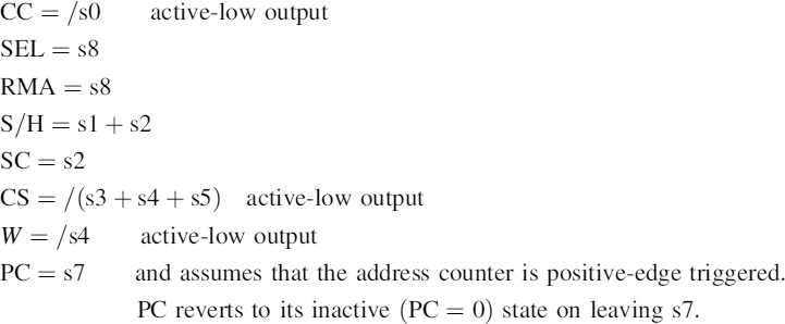
For now, a state diagram can be developed for this basic system as illustrated in Figure 5.7. This is much along the lines of the one developed in Frames 2.4–2.10. In this state diagram, the sequence of control is clear. Once the external system sends a request for the system to start filling the memory with data (st = 1), the following occurs:
- The sample-and-hold circuit is placed into hold mode ready for the ADC (s1).
- The flash ADC is placed into conversion mode and the FSM waits for the end of conversion eoc signal to go high, signifying that a conversion has taken place (s2).
- In s3, the FSM selects the memory device by asserting (low) its chip select input CS. The FSM will move to s4 only when the ADC eoc signal returns to logic 0.
Figure 5.7 State diagram for the DAS.
- In s4, the FSM activates the memory chips write enable signal W (low).
- In s5, the memory write signal is taken high to write the data into the memory device.
- In s6, the chip select is taken high to deselect the memory. This ensures that the memory chip is deselected before the address is changed.
- In s7, the address counter is pulsed by making CC = 1; the address counter is pulsed on the rising edge of this signal. In s7, a check is made to see whether the last memory location has been used (f); if not, the FSM moves around the loop comprising s1 to s7 again.
- This will continue until all the available memory has been filled with data, at which point the FSM will fall into s8 and assert the mf output to the external device.
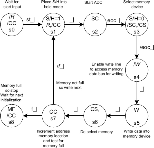
Note that the MF signal could be connected to the interrupt input of the remote device so that it could start the process with st = 1 and be interrupted when the task is complete.
The One Hot equations now follow:
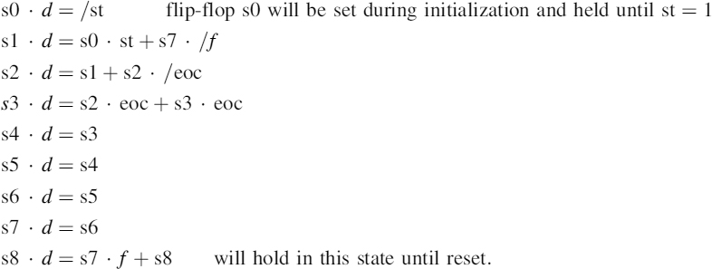

These signals can be used to construct a Verilog file and simulated, as illustrated in Figure 5.8. From Figure 5.8, it can be seen that the FSM loops four times, ending up in s8 at the end of the third loop. Note the control of the memory chip select and write signals and the address counter pulses. Also, at the end of the simulation the memory full mf signal goes high in state s8. The reset is applied to return the FSM to s0.
The system developed in Figure 5.6 allows digitized data to be stored into the memory, but it does not provide any way of getting access to the data once it has been saved. The reader might like to modify the system to allow this to happen, but some thought needs to be given to what device is to be used to perform this operation.
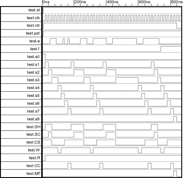
Figure 5.8 Simulation of the data acquisition FSM controller.
The next example illustrates how memory can be controlled in this way.
5.3 A SHARED MEMORY SYSTEM
It is often required to be able to access the data stored in memory via some other controlling device. For example, this could be an external microprocessor to process the stored data in the memory. The example in Figure 5.9 illustrates how this might be done. In this system the memory can be accessed by either the FSM or the external system (which could be a microprocessor or DSP system). The memory is, in effect, ‘shared’. The idea is that during the data-gathering phase, the FSM has sole access to the memory and deposits digitized samples of data under its own control. During the data delivery phase the external device can access the memory, but only when there is data to be read.
The external device must wait for the RMA (read memory available) signal going high, for only when this signal is high will the FSM have disconnected itself from the memory device. Also, when the external device has completed the read memory transaction, and disconnected itself from the memory device, it must send an acknowledge signal ack to the FSM so that the FSM can revert to its initial state. The FSM in this system is the master device. Signals RMA and ack form a handshake mechanism.
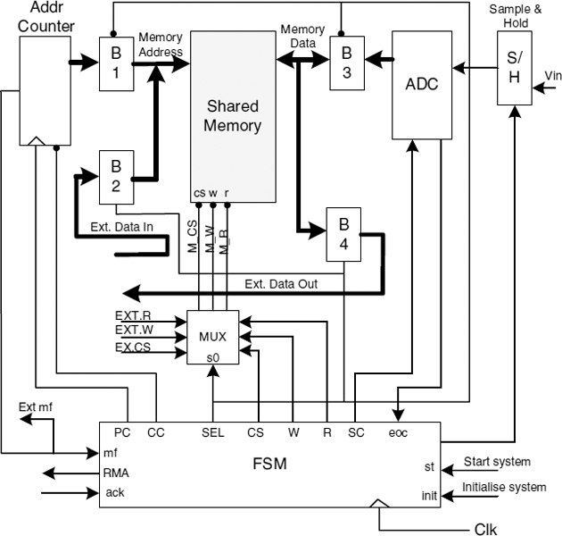
Figure 5.9 Block diagram of a shared memory system.
Note that the FSM uses its SEL signal to control the selection of the tri-state buffers B1 to B4, so that buffers B1 and B3 are selected when SEL = 0. Buffers B2 and B4 are selected by making SEL = 1 to allow the external device to control the memory.
The ‘tri-state’ devices are thus connected to the memory device to allow it to be ‘shared’.
- The tri-state buffers B1 to B4 control the connection of the address and data buses.
The two-way Multiplexer M is used to control the memory device from the two sources (FSM and external device).
- When its control input s0 = 0, the CS, W, and R control lines from the FSM are connected to the memory device. Otherwise, the external device has control of these three signals when s0 = 1.
The following equations describe the behaviour of the multiplexer:
M_CS = CS · /SEL + EXT_CS · SEL
M_W = W · /SEL + EXT_W · SEL
M_R = R · /SEL + EXT_R · SEL.
Note that the handshake signals RMA and ack are mandatory for this system to work, since the external device must not have access to the memory unless it receives the RMA = 1 from the FSM. Likewise, only when the external device has disconnected itself from the memory can it send the ack = 1 signal to the FSM.
The state diagram for this system (Figure 5.10) is very similar to that in Figure 5.7, but has signals to control the memory device connection.

Figure 5.10 State diagram for the shared memory FSM system.
Note that in the state diagram in Figure 5.10 it is assumed that the ADC is slower than the time for the FSM to move from state s3 back round to state s2 and in s3 it waits for eoc to return low before moving to s4.
The equations for this design can be obtained from the state diagram as follows.
D flip-flop d inputs:
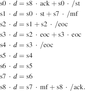
Output equations:
5.4 FAST WAVEFORM SYNTHESIZER
A number of design issues will be covered in this example, including some aspects of interfacing to a microprocessor or microcontroller to an FSM-based design.
A frequency synthesizer is to be developed based around an FSM. The idea here is to be able to transfer a set of data from a microprocessor/microcontroller via a parallel portal into a memory device. Once this is done, the FSM is to read consecutive memory locations and output them to a DAC. A block diagram of the system is illustrated in Figure 5.11.
Note that the waveform data may be any number of data samples in the memory, depending upon the waveform period and sampling frequency. Therefore, the memory full signal mf is actually an ‘end of waveform’ signal, generated by comparing the address bus value with an ‘Address Limit Value’ sent by the controlling device.

Figure 5.11 The fast waveform synthesizer block diagram.
Of course, the total number of waveform samples must be able to fit into the memory device, but the end of waveform must be detected so that when the FSM cycles through to memory location zero the waveform at the DAC output looks continuous and starts at the correct point in the waveform.
In this diagram, the parallel ports to/from a microcontroller, say, are used to provide waveform data to the memory. st is the start input and rp is an input to define record mode (logic 1) or playback mode (logic 0). These two inputs could be from the microcontroller or simply provided as user-activated switches.
5.4.1 Specification
On power up, the FSM looks for st asserted. Then, if the rp is logic 1, it will assert its DRDY output high to let the microcontroller know that it is expecting a data byte. The microcontroller puts a data byte onto the parallel port outputs d0 to d7. The FSM then writes a data byte to the memory device and then lowers its DRDY signal, to let the microcontroller know it has dealt with the data byte. On seeing the DRDY signal go low, the microcontroller lowers its ack signal line to let the FSM know that the transfer is complete. This process continues until the memory is full. Note that memory full depends upon the number of waveform samples placed into the memory device. The microcontroller places a limit value onto the data lines, so that the FSM has a memory limit value to reach. At this point the memory full signal mf will go to logic 1.
If the input rp is turned to the play position, then the FSM will start to send the data in the memory repeatedly to the ADC so that the waveform will be displayed until such times as the st input is disasserted.
A state diagram will be created based upon the specification and then implemented using One Hot equations.
5.4.2 A Possible Solution
This is a relatively complex design making use of a program running on the microcontroller to control the system via the parallel ports.
The state diagram needs two main loop paths: one for record mode and the other for playback mode. By making use of Mealy outputs, it is possible to produce a state diagram using 13 states. This is illustrated in Figure 5.12.
There are, of course other possible solutions, some of which will contain more states (particularly if the outputs are all Moore). This solution makes use of Mealy outputs so that the main part of the loop can be used for both write and read operations. The R and W signals are active-low signals and are dealt with in the manner discussed in Frame 3.26.
A brief description of the state diagram is now given.
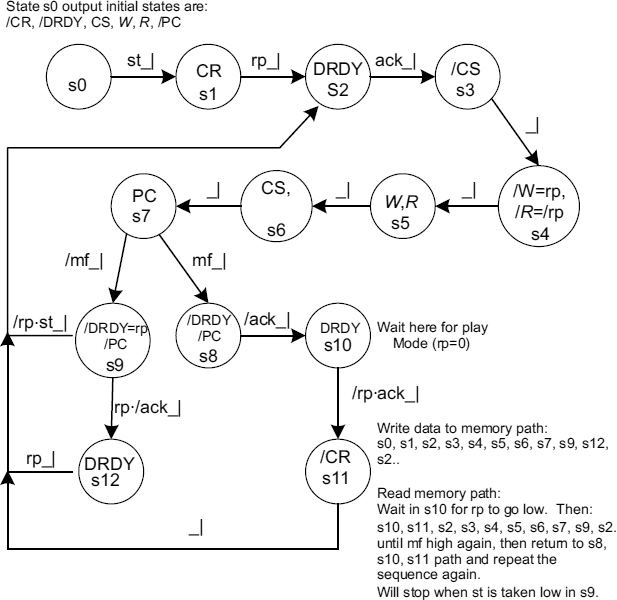
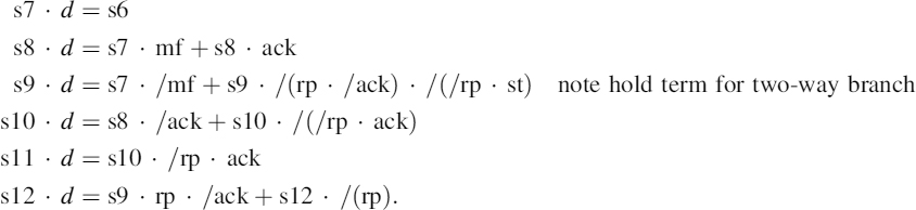
Figure 5.12 One Hot State diagram for the waveform synthesizer FSM.
On operation of the start input st the state machine will leave state s0 to s1 where it will remove the address counter reset CR before moving, on the next clock pulse, to s2 to raise its ready flag DRDY. On receiving the DRDY signal from the FSM, the microcontroller (via its parallel port) will enable the tri-state data buffer connecting the parallel port to the memory data bus so that data can be written to the latter – this by making rp = 1. This will also disable the other tri-state buffer used for reading the memory data. The microcontroller will raise its ack signal to allow the FSM to move to state s3, the memory chip select will be activated (CS = 0) to enable the memory device, and on moving to s4 the memory write W will be lowered, since rp = 1 (write mode). Note that in memory play mode rp = 0 it will be the read signal line that will be lowered in state s4. On moving to s5, the CS and W (or R) will be raised to perform the memory write (or memory read) of that particular memory location.
The FSM will, on the next clock pulse, move to s6 to deselect the memory chip before moving on to s7, where it will raise the PC signal to pulse the address counter. A test will be performed to see whether the memory is full. If the memory is not full, then the state machine will follow the path s7 to s9, where it will lower the DRDY flag if in record mode (rp = 1) and wait for an ack from the microcontroller (this allows the microcontroller to prepare the next data byte to be sent to the memory). On reaching state s12 the state machine will move on to state s2 to repeat the operation for the next memory location. Note, as usual, PC is lowered on leaving s7.
This will continue until all of the memory is full. When this happens, the transition from s7 will be to s8, not s9, and the state machine will send its usual DRDY to zero and wait for acknowledgement from the microcontroller. On receiving the acknowledgement flag ack, it will wait in s10 for the user to set the rp input to zero (indicating that the system is now in playback mode).
In playback mode, the state machine will move to state s11 to reset the address counter and thereby back to s2 to repeat the loop s2, s3, s4, s5, s6, s7, s9, and s2 repeatedly while rp = 0 and st = 1. In this loop, the memory is being read, but now, since rp = 0, the address counter will continue to roll over to zero after running through the memory up to the memory limit value until the start input st = 0.
Note that the FSM waits for ack to be disasserted in states s8 and s9 to complete the handshakes.
A reset can be added to the system to force it back to state s0 at any point in the state sequence.
Development of the One Hot equations from the state diagram can now be undertaken.
5.4.3 Equations for the d Inputs to D Flip-Flops

The output equations follow.
5.4.4 Output Equations

These can all be implemented in Verilog HDL directly.
5.5 CONTROLLING THE FINITE-STATE MACHINE FROM A MICROPROCESSOR/MICROCONTROLLER
In order to develop the program, one needs a programmer's model to illustrate the connection interface between the FSM and the microcontroller.
From Figure 5.13 it can see that the microcontroller needs to use a byte-wide output port to send waveform data to the memory, and two additional bits to form a handshake between the microcontroller and the FSM. There is also a need for a byte-wide output port to send the memory limit value. The main purpose of the microcontroller is to generate the waveform data to be used by the FSM-based synthesizer. It is beyond the scope of this book to go into how this might be done, but the individual digital values could be computed by the microcontroller to be sent to the memory device.
Listing 5.1 illustrates a program fragment for possible execution on the microcontroller. The program is written in C, which is very common for microcontroller programming.
//-- includes needed by the program --------------------------
#include <microcontroller.h> // standard C header file for the particular microcontroller.
//-----printer port register addresses ---------------------------
#define dataport 0x300 // address for port data outputs (change to suit microcontroller)
#define ackdryrp 0x301 // address for handshake bits and rp (change to suit microcontroller)
#define memlim 0x302 // address for the memory limit portal.
#define MAX 1024 // Limit of memory size - can be // changed to suit your requirements. Not used in this example.
unsigned char mem_limit_value; // location to save limit value in.
// C Fuction prototypes used by the program.
void get_data(void); // used to get the data from the FSM.
void Send_data_to_FSM(void); // Use to send data to the parallel port.
int i;
unsigned char inbyte, outbyte;
unsigned char array [MAX];
//--main program function-------------------------
int main(void)
{
    get_data(); // a C function that deals with the data you want to send.
    Send_data_to_FSM(); // see below.
    // could do other things here.
return (0); terminate the C program here.
} // end of main program.
// The C functions now follow.
void Send_data_to_FSM(void)
{
   mem_limit_value = 255; //get the memory limit value to send.
   MemLim = mem_limit_value; // send limit value to its portal.
   for(i=0; i < sizeof(array); i++)
     {
       do { // wait for data ready flag to go low from FSM.
         inbyte = ackdryrp; // input from the ackdry port register.
         inbyte &= 0x01; //mask all bits except the drdy bit.
     } while(inbyte ! = 0x00); //keep on looping until data ready flag set from FSM (active-low).
//---------------------------------------------------------------------
     outbyte = array [i]; //get next data byte to send to FSM from array.
     dataport = outbyte; // send it to FSM.
     ackdryrp |= 0x02; //set ack bit to tell FSM
     do { // wait for drdy to go high again.
       inbyte = acktryrp;
       inbyte &= 0x01;
     } while(inbyte != 0x01);
    }       // end of for loop.
}           // end of C function to send data to FSM.
void get_data(void)
{      // just generate data for a ramp waveform. Simple example.
   for (i = 0; i < mem_limit_value; i++)
     {
       array [i] = i;
     }
}      // end of get_data;
Listing 5.1 Example C code to control the waveform synthesizer.
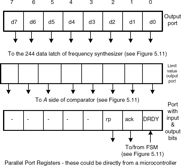
Figure 5.13 Parallel port registers and their bit functions.
Listing 5.1 is very generic and would need to be tailored to a particular microcontroller. It is made up of a main program function main() which calls two C functions.
In this example, the first of these functions, get_data(), is used to create a simple ramp waveform by writing bytes to an array with the line
array [i] = i;
up to a memory limit value. The for loop simply increments the i value from 0 up to mem_limit_val and stores it into consecutive elements of the array. Note, mem_limit_val would be the value sent to the Comparator A inputs in Figure 5.11 to activate the mf signal when the address inputs from the counter were the same as the ‘Address Limit Value’.
The second C function takes the content of the array and sends it to the FSM memory, via the dataport of the microcontroller:
outbyte = array [i]; //get next data byte to send to FSM from array.
dataport = outbyte; // send it to FSM.
ackdry = 0x02; //set ack bit to tell FSM.
To control this operation, and to synchronize the FSM to the microcontroller, the dry and ack signals are used as handshake signals. The microcontroller uses do-while loop constructs to perform these operations.
do { // wait for data ready flag to go low from FSM.
  inbyte = ackdry; // input from the ackdry port register.
  inbyte &= 0x01; //mask all bits except b1, the dry bit.
} while (inbyte != 0x00); //keep on looping until data ready flag cleared from FSM.
The do-while loop is used to read in the status of the drdy bit (inbyte = ackdry). This is then stripped of all bits except the bit b0 dry with the instruction inbyte &= 0x01. This is compared with 0x00, and if not equal (!=) causes the do-while loop to repeat until dry is set to zero, making the while(inbyte ! = 0x00) false and causing the program to fall out of the do-while loop. In this way, the program cannot get past the first do-while loop until dry = 0. The second do-while loop looks for drdy to go high before getting the next data value from the array to send to the FSM.
The program continues to repeat the actions again until all the data in the array have been sent to the FSM memory.
This short description should give you an insight into how the waveform data can be sent to the FSM. For the generation of more complex data, e.g. sine waves and exponentially decaying sine waves, a more complex get_data() function would need to be developed.
5.6 A MEMORY-CHIP TESTER
An FSM-based test system can be used to test memory chips prior to fitting them onto a circuit board. Fitting memory chips direct from the manufacture can be expensive if a faulty memory device is discovered at the final testing stage of production and the defective memory has to be removed, particularly if the device is soldered directly onto the printed circuit board.
The memory tester could typically be used in the Goods Inward Department of a factory that was using a large number of memory chips. This would allow each memory chip to be tested and could form the basis of a quality control on overall quality of the memory chips received from a particular manufacturer. The memory tester should be easy to use by an unskilled operator and function as a ‘go–no-go’ tester.
The basic idea is to write some data into the memory chip and read the data back to check that they are the same. In such a test, any location found to be faulty would deem the memory chip to be faulty and it would, therefore, be rejected.
Figure 5.14 illustrates the block diagram for the memory tester. In this version, the data 55 hex (0101 0101 binary) is written into each consecutive memory location, then read back and compared using the digital bitwise comparator. The bitwise comparison follows the Boolean equation
![]()
where ^ is the exclusive OR operator. This operation is (with the NOT operator /) the exclusive NOR i.e. exclusive OR negated. n represents the bit being ex-NORed. The ex-NOR operation is shown below for completeness.

Figure 5.14 Block diagram for the memory tester.

The system can be started by raising input st, the start input. The FSM will control the memory operations and test the fab input to determine whether what was written is the same as what is read.
A more sophisticated version could be developed in which each memory location is tested with the data 55 hex, then retested with the data AA hex to check for adjacent stuck at 1 or 0 faults. Other tests, such as checking adjacent memory locations to test for inter-memory location faults, could also be included; however, for this simple tester the 55 hex data will suffice.
The output ‘A = B’ connected to the fab input of the FSM is the logical product of all 8-bit comparisons bit0-bit7; so, if all exclusive NOR outputs are at logic 1, then the ‘A = B’ output will be logic 1. This is expressed mathematically as

Figure 5.15 State diagram for the memory tester.
![]()
where An and Bn are bit n on each A and B input and Π indicates that each /(An ^ Bn) is ANDed (i.e. product).
The state diagram for the memory tester is illustrated in Figure 5.15. In this state diagram, the initial states of the outputs have not been shown, but they can, of course, be deduced from the state diagram, since each state shows the change of outputs. So, for example, RC = 0 in s0, then in s1 it becomes RC = 1, and remains so for all other states in the diagram. Likewise, CS = 0 in s1, so it must be CS = 1 in s0. Following on, the other initial values in s0 are P = 0, ERROR = 0, OK = 0, W = 1, RD = 1. Note that the state diagram has been allocated a set of secondary state variables ABCD. These are not needed in the One Hot design, but they are used later on when a comparison with the more conventional method used in Chapter 4 is made.
In states s1, s2, and s3, the data 55 hex is written into the current memory location pointed to by the address counter. States s4, s5, and s6 are used to read the memory location and in state s6 the FSM tests fab. If fab = 1, then the memory location is OK and the FSM proceeds to pulse the address counter in s8 and checks to see whether all memory locations have been tested in state s9. If not, the whole process is repeated.

Figure 5.16 The One Hot equations for the memory tester.
In the case of a good memory chip the FSM will loop around the states s1 to s9 repeatedly until the memory full indicator forces the FSM into state s10. The only way out of this state is via a system reset. This ensures that, after a memory test, the system waits for operator intervention.
At any time a memory location is found to be faulty, the FSM will drop into s11 and stop. The only way out of s11 is via a system reset.
The One Hot equations for the memory tester are given in Figure 5.16.
The state diagram of Figure 5.15 has a Moore output P. The rising edge of P will clock the address counter on entering state s8, P being lowered on leaving s8. The memory chip enable is disasserted in s7 prior to this action. The address counter only responds to the rising edge of P, so that on the next clock pulse the state of full can be tested in state s9.
5.7 COMPARING ONE HOT WITH THE MORE CONVENTIONAL DESIGN METHOD OF CHAPTER 4
In Figure 5.15, a set of secondary state variables has been provided so that this example could be implemented with four flip-flops. If this was done, the D-type equations would be as shown in Figure 5.17.
This, of course, uses the same technique used in Chapter 4, not the One Hot method. You might like to complete the equations and minimize to compare with the One Hot solution above.
It is useful at this stage to do a comparison between the One Hot method and the method that uses secondary state variables in the last example.

Figure 5.17 Memory tester design implemented with four flip-flops.
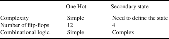
The One Hot design is simple, uses more flip-flops but has simple combinational logic. The design using secondary state variables needs to be assigned a unique secondary state coding and has more complex combinational logic. However, it requires only four flip-flops. The One Hot arrangement needs 12 flip-flops and 15 gates, whereas the secondary state implementation needs four flip-flops and 13 gates. A hidden advantage of the One Hot design is that it makes more efficient use of the space on an FPGA device.
5.8 A DYNAMIC MEMORY ACCESS CONTROLLER
DMA controllers are used in some computer systems in order to allow data to be moved from one part of the memory system to another or from memory to a peripheral device (such as a printer or disk drive for example). If these data moves were done by the computing microprocessor, this would tie the microprocessor up and slow down the computing system. The PC has a special chip called the DMA controller, the 8257 (now largely integrated into an ASIC device), that performs these tasks.
This next example gives some idea of how a simple DMA controller could be developed around an FSM. The design could be integrated into an FPGA.

Figure 5.18 Block diagram of a possible DMA controller.
Figure 5.18 shows a possible arrangement for a DMA controller. The source and destination addresses need to be supplied by the microprocessor, as well as the number of words to be transferred (Byte Counter). The size of the data could be bytes (8 bits), words (16 bits) or even double words (32 bits), since the design can be scalable. In this design, it is assumed that these are delivered via an input port, but registers could be provided with address decoding for a memory-mapped DMA controller.
The dashed line marks the boundary of the DMA controller. The Memory Pool/Peripheral Device is external.
A DMA controller must be able to isolate itself from the memory/peripheral device when not being used, and this is achieved using tri-state devices.
Essentially, the DMA controller is designed to respond to an input st. At this point it should accept the source, destination addresses, and the number of words/bytes to be transferred. Then it should interrupt the microprocessor to let it know it is about to take over the memory/peripheral. The microprocessor will then isolate itself from these devices and send the load signal high to let the DMA controller know this has been done, and also provide it with the source/destination addresses and the byte count. At this point, the DMA controller will load the source, destination counters, and the byte counter.
Note that the registers are clocked synchronously with the system clock (on negative edge of clk) but enabled via the FSM output ec. The DMA controller now has enough information to carry out the transaction. This involves:
- Selecting the source address and reading its content into a buffer.
- Selecting the destination address and depositing the buffer content into this address.
- Decrementing the byte counter and advancing the source and destination address counters.
- Repeating 1 to 3 until all data transactions are completed (indicated by the byte counter reaching zero).
The DMA controller can now be developed in more detail. Clearly, a parallel-loading up counter is needed for both the source address and the destination address. Also, a parallel-loading down counter is required for the byte counter. Appendix B describes how these can be simply designed in detail.
Since the source and destination counter outputs need to be connected to the address bus, they should have tri-state buffers to isolate them from the memory/peripheral address bus when the DMA controller is not in use. The source or the destination address counters are used one at a time to avoid bus contention. The DMA controller will also need a data register and buffer connected so that the data read from one memory location can be fed to another memory location. This data buffer acts as a holding register within the DMA controller. The buffer needs to be isolated from the memory/peripheral data bus when not being used. Finally, all these internal devices need to be controlled by the FSM.
Figure 5.19 illustrates a possible block diagram for the DMA controller. Figure 5.19 shows a lot of detail and contains internal signals used by the FSM to control the operation of the DMA controller.

Figure 5.19 Detailed block diagram for the DMA controller system.
The FSM must carry out the transactions 1 to 4 detailed above. These, in turn, need to be defined in terms of the actions required to control the hardware in Figure 5.19. These actions will involve:
- Waiting for the start signal st.
- Providing an interrupt to the microprocessor to get it to isolate itself from the memory.
- Waiting for a load signal from the microcontroller; when obtained, loading the source, destination, and byte count into the relevant counters.
Then:
- 4. The source memory needs to be selected and data read from the memory into the data holding register.
- 5. The source address needs to be isolated from the memory and the destination memory selected.
- 6. The data in the holding register needs to be transferred into the output buffer B3 and stored into the memory destination address.
After all this:
- 7. The byte counter needs to be decremented and checked to see whether all bytes of data have been transferred.
- 8. If there are more bytes to transfer, then the FSM needs to repeat 1 to 7 again. This is to continue until all bytes are transferred, indicated by the byte counter being decremented to zero.
The state diagram for the DMA controller can now be developed. The final form of this state diagram is illustrated in Figure 5.20. Study this diagram together with the diagram of Figure 5.19 to see how the DMA controller is controlled from the FSM.

Figure 5.20 The state diagram for the DMA controller FSM.
A number of points need to be considered:
- When reading the source memory location (states s4 to s7), the chip select and read signals CE and R need to be kept active while data is transferred into the holding register (s6 and s7) before they are disasserted (to their high state in states s8 and s9 respectively). This is different to the way in which memory read cycles have been done in other examples.
- Writing the data from the output buffer follows the more usual arrangement, whereby the chip is selected (s11), then write is selected (s13), and finally both CE and W are deselected (s14 for W, s15 for CE) to write the data into the memory destination location.
- Note that the source, destination, and byte count registers are enabled via the EC output from the FSM in state s16, and that the system clock clk clocks the data on the negative clock edge.
The One Hot equations can now be determined.
5.8.1 Flip-Flop Equations

5.8.2 Output Equations
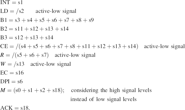

Figure 5.21 Simulation of the DMA FSM block.
The FSM block is simulated in Figure 5.21. In this simulation, the main loop comprising of states s3 to s17 is traversed twice. On the second loop, the done input is true (logic 1) and the FSM moves to s18 before returning back to state s0. This proves the operation of the FSM.
5.9 HOW TO CONTROL THE DYNAMIC MEMORY ACCESS FROM A MICROPROCESSOR
The DMA system is started with the start input, which in the previous design would need to be via an output port from the microprocessor. This is sometimes useful, since it avoids the need for address decoding logic.
A more appropriate way would be to have this signal via the memory (or I/O map) of the microprocessor. Normally, this would require using a byte-wide port.
In Figure 5.22, the start signal st is generated by a microprocessor using a spare address location. The address used here is 380 hex or 11 1000 0000 binary for this purpose. A typical memory or Input/Output access cycle is illustrated, from which it is clear that when the chip enable Ce and the IOW are both low (as would be generated by the microprocessor) the output from the address decoding logic corresponding to the address 380 hex would go high. The next clock pulse from the microprocessor clock (T3 rising edge) would clock the st value into the D-type flip-flop.
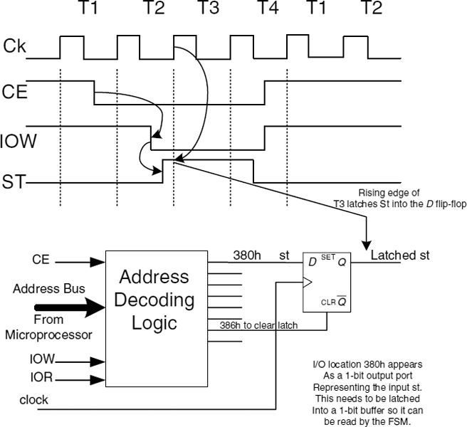
Figure 5.22 Generating a start signal from a microprocessor for the FSM.
The microprocessor would need to use an address (386 hex in this case) to reset the D flip-flop at an appropriate time. However, before this, the microprocessor would need to wait for the ACK response from the FSM.
Figure 5.23 illustrates how this could be done, together with the generation of the st signal. In Figure 5.23, the additional data latch is used to store the state of the FSM output ACK. The FSM raises the ACK signal line and clocks it into the data latch with the pak signal (added to the FSM for this purpose). The microprocessor can read the ACK signal by addressing 381 hex, which takes the tri-state buffer out of its tri-state, thus setting bit d0 of the data bus to that of the ACK signal stored in the D-type flip-flop during the memory or IO read cycle of the microprocessor.
The ACK signal will be read by the microprocessor in the T4 state on the rising edge of CE and IOR signals during the read cycle (see Figure 5.24) into an appropriate internal register within the microprocessor.
The state diagram fragment shown in Figure 5.25 shows the relevant state sequence needed to use the microprocessor memory or IO mapped control. Note that this can be used with the other states of Figure 5.20 in the DMA controller.
Of course, this example is based upon hypothetical microprocessor bus timing, but it does illustrate a possible method.

Figure 5.23 The whole arrangement for writing to and reading from the FSM.
5.10 DETECTING SEQUENTIAL BINARY SEQUENCES USING A FINITE-STATE MACHINE
A very common requirement in communication and computer network systems is to detect binary sequences. The following example illustrates the idea and can be scaled up and changed to detect other sequences.
One common approach is to insert a shift register into the transmission line and use digital comparators to detect the incoming binary stream after the number of bits corresponding to the binary code have been shifted into the shift register. This, of course, introduces an n-bit delay. So, to detect a 4-bit code introduces a 4-bit delay. If the code to be detected is longer (e.g. 8 or 16 bits), or other devices are to be added to the line to detect other codes, then the delay increases.
An alternative approach is to monitor the transmission line passively in real time and process the binary bits in an FSM. This will not introduce any delay.
Consider a system such as the one shown in Figure 5.26. In this system, the FSM monitors the input binary sequence continuously looking for the sequence d = 1101 (this could be any sequence in practice, but this one will suffice).
The FSM needs to synchronize to 4-bit data streams; in Figure 5.26, the first data stream is 1011, then the next 1101 (the required sequence), followed by the sequence 0011. The output M should go high at the end of the sequence 1101.
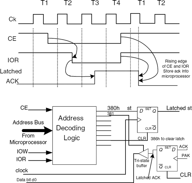
Figure 5.24 The arrangement for reading the ACK signal from the FSM.

Figure 5.25 Illustration of the state sequence needed for using the microprocessor memory or IO mapped control.

Figure 5.26 Binary sequence detector.
The best way to develop the state diagram for this application is to start with a state diagram that follows the required sequence; see Figure 5.27, where the required sequence d = 1101 is detected in state s4, where the FSM stops.
However, it is necessary to go through the 4-bit sequence and return to state s0 if the required sequence is not detected. This is shown in Figure 5.28, where the state diagram is seen to cater for all possible combinations.
For example, an input sequence of d = 1100 would follow states s0, s1, s2, s3, s0. An input sequence 1111 would follow states s0, s1, s2, s7, s0; and so on. In this way, the FSM keeps in step with the incoming binary sequence.
Once the correct sequence is found, the FSM will stop in state s4.
The FSM clock needs to synchronize with the middle of the data bits being monitored; this could be done using the same technique used in the asynchronous receiver design of Figure 4.20 in Section 4.7.
The design can be implemented using the One Hot method, resulting in the following equations:
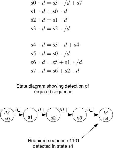
Figure 5.27 State diagram segment to detect required sequence.
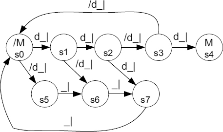
Figure 5.28 State diagram completed for all possible input combinations.
and output
M = s4.
This design can be built up in Verilog and simulated as illustrated in Figure 5.29. This simulation runs through all possible paths of the state diagram in order to test out the FSM logic.

Figure 5.29 Simulation of the sequence detector.
In the first sequence, the simulation is seen to follow the sequence s0, s5, s6, s7, s0. This is followed by the sequence s0, s1, s2, s3, s4, with M = 1. After this, the FSM is reinitialized back to s0 for another sequence by lowering rst and pst (asynchronous initialization). Then, the sequence s0, s1, s2, s7, s0 occurs. This is followed by other sequences to complete the testing of all paths through the state diagram. Note that during the last sequence, i.e. s0, s5, s6, the asynchronous initialization forces the FSM back to s0.
The system could be modified so that it continues indefinitely to monitor the incoming sequence, providing an M = 1 output whenever the correct sequence is detected. This can easily be done by making M a Mealy output in state s3, so that
M = s3 · d.
If d is not 1 in state s3, neither is M. Of course, state s4 is no longer needed in this case.
Figure 5.30 shows the final state diagram In Figure 5.30, the M output is made a Mealy output in s3 so that the FSM can return to s0 after any sequence. In this way the FSM can continue to monitor incoming sequences forever and remain synchronized to the 4-bit pattern.
In Figure 5.31, the sequence detector can be seen to return to s0 after detecting the 1101 sequence. Note: the output M is only 1 when d = 1.
The same technique could be applied for longer sequences, making use of more states and more flip-flops.
One limitation of the sequence detector of Figure 5.30 is that it is limited to detecting one particular binary sequence, in this case 1101. It would be more useful to have an FSM that could accept any binary sequence without having to redesign the state diagram.
In Figure 5.30, the FSM looks at the line bits with the same variable d. Instead, the d input could be compared bit by bit with a number of digital 1-bit comparators (exclusive NOR gates), each one having a bit of the code to compare the incoming bits with. Figure 5.32 illustrates a possible arrangement. In this case, a more realistic 8-bit code is to be detected.
Also note that the code to be detected can be stored into a data latch prior to starting the detection process. This system can be used to detect up to 255 different codes (assuming the code 0000 0000 is not used).
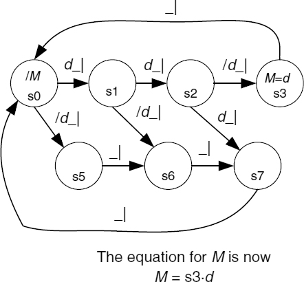
Figure 5.30 Final state diagram for continuous monitoring for the d = 1101 sequence.

Figure 5.31 Final simulation of the sequence detector.

Figure 5.32 Comparators used to compare each bit with a pre-stored code.

Figure 5.33 Full system of the general 8-bit binary code detector.
The code C0 to C7 is loaded into the data latch and is presented as a registered code RC0 to RC7 and connected to one input of the single-bit digital comparators.
The input bits from line d are all connected to the other comparator inputs, so that eight compared bits d0 to d7 are available to the FSM.
Figure 5.33 shows the full system: an additional input to the FSM en is used to start the system and an additional output LD is used to latch the code value to be detected.
The state diagram for the FSM is illustrated in Figure 5.34. The state diagram of Figure 5.34 follows the same basic idea developed in the state diagram of Figure 5.30, but for a byte-wide code. Note that rather than compare each d bit at the line, the FSM now compares each bit after it has been compared with the desired code with the 1-bit comparators, first bit d0, then d1, through to bit d7.
Now the FSM is a fixed sequence that can detect any possible 8-bit code. All that needs to be done is load the required code into the data latch before starting the detector. The system can be disabled at any time by disasserting the input en. This will cause the system to stop at the end of the current sequence then return to state s0.
A little thought shows that the same FSM could be used to detect a number of different codes one after the other by simply changing the codes in sequence.
One aspect of the system not yet discussed is how to synchronize the system to the line bit stream. One way to do this would be to start the system off with a synchronization bit stream code, say 10101010xx, prior to starting the code detection process, where x is an additional bit that could be either 0 or 1. This could be broadcast by the sender.
The additional bits are needed to allow the FSM to load the data latch with the desired code to be detected. The same FSM could be used for this, since all that needs to be done is to load up the synchronization code. Once the synchronization byte is detected (via M) the code to be detected would be loaded into the data latch and the code detection sequence started.

Figure 5.34 The state diagram for the FSM-based type-wide code detector.
The One Hot equations can be obtained directly from the state diagram of Figure 5.34:

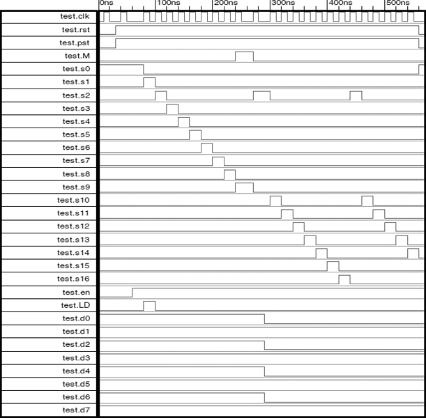
Figure 5.35 Simulation of the FSM sequence detector using a code 11001011.
with outputs
Of course, the code to be detected could be any length, since the state diagram could be developed for any particular length following the same basic idea.
The simulation in Figure 5.35 shows the system in which the code to be identified is 11001011. This code is first loaded into the latch via the C0 to C7 inputs. The simulation then presents a number of serial d input sequences, with the last one being the one the system is trying to detect. The M output goes high at the end of this sequence.
The complete system, comparator, octal latch and FSM as connected up in Figure 5.33 is simulated and illustrated in Figure 5.36. Only the system inputs and output signals are visible here (see block diagram in Figure 5.33), along with the FSM state sequence so that the state sequence of the state machine in Figure 5.34 can be followed. Note that the sequence to be detected in this simulation is C[7:0] = 11001011. This sequence is detected at the end of the simulation at around 700 ns into the simulation, and can be clearly seen in the bottom two signals (d input and M output).

Figure 5.36 Simulation of the complete 8-bit sequence detector.
5.11 SUMMARY
This chapter has explored the use of the One Hot technique to implement FSMs. These are particularly useful for implementation in FPGA devices and have the advantage of not requiring secondary state variables. The hand calculations are much easier to perform and can be converted into Verilog HDL easily. Also, owing to the large size of FPGAs, large FSM designs can be implemented without the need to consider secondary state variable assignment.