
6
Introduction to Verilog HDL
6.1 A BRIEF BACKGROUND TO HARDWARE DESCRIPTION LANGUAGES
This chapter will introduce the fundamental aspects of what has become an essential tool for the modern digital system designer, namely the HDL. There are many different HDLs used for a variety of purposes. Some are best suited to low-level design, making use of logic gates and Boolean equations (e.g. ABEL [1]), while other so-called system-level languages are intended to aid the design and verification of entire systems comprising both hardware and software (examples are SystemC [2] and SystemVerilog [3]).
In addition to the support for digital systems, in which events and values are modelled in discrete terms, HDLs have evolved to encompass the realm of continuous time or analogue behaviour. Apart from mentioning these languages in passing, this book will not consider the details of this category of HDL.
The HDL described in this book is the very popular, and relatively easy-to-learn, Verilog HDL [4], often referred to as ‘Verilog’ or ‘HDL’ (the names ‘Verilog’ or Verilog HDL' are used interchangeably throughout this book). The language has a considerable user base among the digital design communities within both industry and academia across the globe. Verilog HDL is unique with regard to the breadth of support it provides for describing and simulating digital systems. Using built-in models of metal oxide–semiconductor (MOS) transistors, the language allows digital circuits to be described at the so-called switch level, where individual switches can exhibit detailed timing and signal strength behaviour. The switch level is very close, in representative terms, to the actual physical implementation of the digital integrated circuit, this makes Verilog HDL the first choice of language used to verify designs beyond the circuit level. At the other extreme, the high-level language constructs contained within the language facilitate the use of a more abstract and, therefore, powerful representation known as behavioural or register transfer level (RTL) in which the design is represented by storage registers and operations involving the movement and processing of information stored in them. It is perhaps the latter capability that makes Verilog HDL and other similar languages the only effective way of dealing with the complexities of contemporary digital design.
The Verilog HDL started out as a proprietary tool in the 1980s, but soon gained widespread popularity as digital integrated circuits and systems became more complex. Consequently, it was introduced into the public domain and subject to standardization by the IEEE in the mid 1990s. The majority of the examples used in this book make use of the Verilog HDL defined by the IEEE Standard 1364-2001 released in 2002. This version of Verilog HDL introduced many new powerful features, along with some cosmetic changes, bringing it in line with one of the other most popular HDLs, namely VHDL (Very High Speed Integrated Circuit Hardware Description Language) [5].
The two most widely used HDLs, i.e. Verilog HDL and VHDL, despite sharing the same acronym, differ in terms of syntax and general appearance, the latter being similar to the Ada programming language [6] and the former having some C-like features. Despite these cosmetic differences, the two HDLs share very similar semantics and tend to be used in the same manner towards achieving the same eventual goal of designing and implementing a cost-efficient digital system that meets the specification in terms of performance and economics.
In addition to their use in design simulation and verification, both Verilog and VHDL can be used as the input language to the automated process of hardware creation known as logic synthesis [7]. The vast majority of digital circuits implemented in actual hardware have been synthesized from a design description written in one of these languages. Modern logic-synthesis software tools are highly reliable, producing optimum and efficient logic circuits often implemented in the form of programmable logic. It should be noted that the role of the digital designer is no less important, however, despite the availability of such tools. What has happened is that the designer is now able to work at a higher level of abstraction, making use of the expressive power of the HDL to create ever more complex designs, while the detailed issues and processes surrounding implementation have been largely automated.
The use of design languages is now well established and the modern electronic designer needs a working knowledge of at least one of the popular HDLs to compete in the employment market. Migrating designs between one particular HDL and another is a relatively straightforward task, once the fundamentals have been mastered. It is far more challenging to learn and master an HDL from scratch for the first time, and apply it to a real-world design problem, than it is to convert a given design into an alternative language, having already mastered an HDL.
As mentioned previously, the huge growth in the use of HDLs such as Verilog HDL and VHDL, along with the constant increase in complexity and integration of hardware and software, brought about by the advances in microelectronic technology, has resulted in the development of what are referred to as system-level languages such as SystemC [2] and SystemVerilog [3].
While SystemC has been developed around the popular C++ language and, therefore, lacks support for low-level digital design, SystemVerilog is a superset of Verilog HDL and, therefore, possesses all of the digital hardware modelling capabilities of Verilog in addition to the higher level data abstraction and software integration needed by today's system-on-a-chip designers.
By learning Verilog HDL, therefore, the digital designer is setting down the foundations for a long and prosperous career, with the comfort of knowing that support exists within the design tools and languages for the ever more complex designs of the future.
To summarize this section, here are some of the key advantages of using an HDL such as Verilog HDL:
- Technology independence – designs written in an HDL are largely independent of the target technology and, therefore, future-proof.
- Textual descriptions are concise, unambiguous and self-documenting.
- Standard language promotes design reuse and portability between design tools.
- Textual descriptions replace or augment schematics.
- Automated design – logic synthesis tools accept designs written using an HDL.
- High-level design – the designer is freed from the tedium of gate-level design to concentrate on system-level aspects.
6.2 HARDWARE MODELLING WITH VERILOG HDL: THE MODULE
In Verilog HDL, the basic unit of hardware is known as a module. In common with C-language functions, modules are free standing and cannot, therefore, contain definitions of other modules. A module can be instantiated within another module, however, in a similar manner to which a C function can be called from another C function; this provides the basic mechanism for the creation of design hierarchy in a Verilog description.
Listing 6.1 shows the basic layout of a module:
module module-name(list-of-ports);
  local wire/reg declarations
  parallel statements
endmodule
Listing 6.1 Basic layout of a module.
Note that in this and subsequent listings all keywords are shown in bold. The hardware description is enclosed by the keywords module and endmodule, the former being immediately followed by the name of the module and a list of ports enclosed in parentheses. (Some modules do not require ports; therefore, the list-of-ports is empty.)
Note that the semicolon at the end of the first line (the module header) is always required, but no semicolon is required after the bracketing keyword endmodule.
Within the module header, the list-of-ports enclosed between the parentheses fully specifies the size (number of bits) and direction of the ports (input or output, etc.), along with the name of the port.
In this manner, the first line of a module contains all of the details of the module that are visible from outside, i.e. the module header represents the interface specification or module prototype.
Immediately below the module header, items that are to be used within the confines of the module are declared. The second line of Listing 6.1 shows the most common local objects to be reg and wire; these represent internal storage and/or connections used within the module. Consistent with other languages, Verilog requires that all objects must be declared before they are referenced; therefore, this means that they tend to be located at the top of the module body. The local wire and reg objects represent signals used within the module to link together the logical elements described by the so-called parallel statements. The term ‘parallel statements’ refers to the manner in which this group of statements executes during a simulation, i.e. concurrently, in a manner similar to that of real digital hardware. The parallel statements describe the behaviour, structure and/or data flow of the design encapsulated by the module. They can take a variety of forms; among these are primitive gates, module instantiations and continuous assignments, all of which will be described in detail in due course.
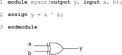
Figure 6.1 A simple module.
A Verilog module description consists of case-sensitive ASCII text, the file containing the text of a module with a given module-name is conventionally stored under the filename ‘module-name.v’. An example of a very simple module is shown in Figure 6.1. The listing in the figure includes line numbers that are for reference purposes only; they must not appear in the actual source text.
As shown in Figure 6.1, the module describes a two-input exclusive-OR gate named myxor having single-bit inputs a and b and an output y. The names and direction of the module ports are specified by the comma-separated list enclosed within parentheses on line 1. The ports of a Verilog module have a default width of 1 bit, and in some cases a port may need to be both an input and an output, i.e. bidirectional. Verilog uses the reserved word inout to specify a bidirectional port.
The functionality of the module given in Figure 6.1 is defined by the so-called continuous assignment statement on line 2, assigning the output y the expression a^b (where ^ is bit-wise exclusive-OR in Verilog). The keyword assign is used to indicate a continuous assignment. Such a statement creates a static binding between the expressions on the left- and right-hand sides of the = operator; it is most commonly used to describe combinational logic.
Despite the similarity with an assignment used in the C language, the continuous assignment on line 2 in Figure 6.1 is a parallel statement; this means that it is constantly active and awaiting events on either of the input signals a and b to trigger its execution. Such events would depend on the activity of external sources applied to the module inputs.
Specifically, whenever a change in value occurs on either or both of the inputs a and b, the expression on the right-hand side of the assignment on line 2 is evaluated and the result is assigned to the target of the continuous assignment on the left-hand side of the = operator (output y) at the start of the next simulation cycle.
A module may contain any number of continuous assignment statements, all of which act in parallel and, therefore, may be written in any order.
Figure 6.2 shows an example of a module containing multiple continuous assignments. Such a description is sometimes referred to as a dataflow style description. The Verilog source describes the logic diagram shown below the text in the figure. In this example, each gate is modelled by a separate continuous assignment on lines 7, 8 and 9. An alternative would have been to describe the logic using a single statement such as
assign F = ~((A & B)|(C & D));
The above assignment illustrates the similarity between Verilog and the C language in terms of the bit-wise logical operators: inversion (~), logical AND (&) and logical OR (|). Also, note the use of parentheses in the above assignment, these force the order of operator evaluation to reflect the logical structure being described.
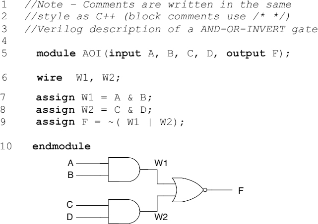
Figure 6.2 A Verilog AND-OR-INVERT module.
Note that the continuous assignment statements on lines 7, 8 and 9 could have been written in any order without changing the behaviour of the logic, internal single-bit wires (declared on line 6) are used to connect the outputs of the two AND assignments (lines 7 and 8) to the inputs of the two-input NOR assignment. The order of execution of the continuous assignments on lines 7, 8 and 9 is determined by events on the primary inputs A, B, C, D and internal wires W1 and W2.
For example, if input A changed from logic 0 to logic 1, this event on A would cause the assignment on line 7 to execute. This, in turn, would cause the value on wire W1 to change from logic 0 to logic 1, assuming input B was already at logic 1. It should be noted that the event on W1 occurs at the same time as the event on input A, since the continuous assignment does not specify any propagation delay. However, the simulator updates signals using a mechanism that involves discrete cycles known as simulation cycles, in which signals are updated as a result of assignment execution.
An infinitesimally small delay, sometimes referred to as delta delay, elapses each time the simulation cycle advances. So, if the event on input A occurred at a time of 10 ns, the resulting change in wire W1 would occur at a time of 10 ns + 1d, where d represents ‘delta’.
Referring back to Figure 6.2, an event on W1 has the effect of triggering the continuous assignment on line 9, which, depending on the value of W2, may or may not result in a change in the module output F. If a change in F were to occur, it would be at a time of 10 ns + 2d, due to the one-delta introduced by the assignment execution.
A wire is a particular case of the more general category of Verilog objects known as nets, all of which share the common requirement of having to be driven continuously, either by a continuous assignment or by virtue of being connected to the output of a primitive gate or module instantiation.
Note: the left-hand side, or target, of a continuous assignment statement must be a wire.
The ports of a module (A, B, C, D and F on line 5 of the example shown in Figure 6.2) are also wires by default; as such, they may appear on the left- or right-hand sides of continuous assignments, depending on whether they are outputs or inputs respectively. Unlike some HDLs, the Verilog language allows ports that have been defined as outputs to appear on the right-hand side of an assignment. This flexibility is included to reflect a common situation in hardware, where a module output signal is internally fed back into an input within the same module.
Figure 6.2 also shows the format used in Verilog for adding comments to a description. Lines 1, 2 and 3 illustrate the similarity between Verilog comment delimiters and those used by the C and C++ languages. Comments are a useful tool for adding documentation to a design description.
The next example of a Verilog module illustrates several additional aspects of the language not yet mentioned.
Figure 6.3 shows a very simple Verilog description of a 4-bit binary adder along with its corresponding symbolic representation. The module header, spanning lines 1, 2, 3 and 4, shows how multi-bit ports are defined. In this case, the inputs a and b and the output sum are all 4 bits wide, being represented as buses on the symbol.
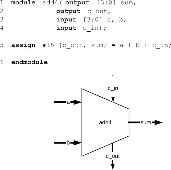
Figure 6.3 Verilog module and symbol for a 4-bit adder.
For example, line 3 of the listing given in Figure 6.3 defines two input ports each having 4 bits ordered 3 down to 0:
input [3:0] a, b,
Ports having the same direction and width can be listed together or on separate lines, whichever is preferred. The expression [3:0] is the bit range of the port; for mathematical purposes, the left-hand bit (in this case bit 3) is always assumed to be the most significant bit.
The module presented in Figure 6.3 is described by a single continuous assignment statement situated on line 5:
assign #15 {c_out, sum} = a + b + c_in;
The above assignment gives some indication of the expressive power of an HDL such as Verilog. To describe an adder, it is simply a case of adding the three input port values together using the built-in + operator whenever any of the inputs change, and continuously assigning the result to the outputs. If required, the adder could also have been described in terms of Boolean equations, logic gates or even individual MOS transistor switches, such is the flexibility of Verilog. There are a couple of important points concerning the above assignment that are worth highlighting at this point:
- The expression on the right-hand side of the assignment operator performs an unsigned addition by default.
- Since a and b are referred to without specifying a bit range, their entire 4-bit values are added along with the single-bit carry input c_in.
- The carry input c_in is automatically added to the least significant bits of a and b (a[0] and b[0]).
- The result produced by adding the three inputs is potentially 5 bits in length; therefore, the target of the continuous assignment is the concatenation of the outputs c_out and sum (using the { } operator), with c_out occupying the most significant bit position (bit 4).
- The inclusion of #15 after the keyword assign indicates a delay of 15 time-units between any input change and the resulting change in the outputs. Time delays are described in more detail in Chapter 7.
In all of the above examples of Verilog modules, all the objects representing digital signals are of type wire. This includes both the internal signals and the module ports. This is due to the simple combinational nature of the examples considered thus far: each module has defined a set of simple combinatorial relationships between the inputs and outputs; there is no need to store any values. Unconnected wires are effectively undriven and, therefore, are assigned the high-impedance value z.
In addition to wires, Verilog provides the reg (short for register) type variable to describe signals that have the ability to retain, or store, the last value assigned to them.
In common with wires, the reg-type signal defaults to 1 bit, but it can also be defined as having multiple bits using the same notation as wires, as illustrated by the following example:
reg [7:0] count; //an 8-bit register variable
The use of the reg object will be considered in detail in Chapter 7.
6.3 MODULES WITHIN MODULES: CREATING HIERARCHY
An important tool used by software engineers is so-called top-down design. Simply described, this involves breaking a complex problem into a set of clearly defined sub-problems, which may in turn be further subdivided into yet simpler problems. In the C/C++ languages, and others, the basic unit of execution is the function or procedure; these self-contained blocks of code are intended to perform a relatively simple task. The software engineer will create the functions required to implement the low-level tasks and make use of them in higher level functions by means of the function or procedure calling mechanism. In this manner, a complex software application can be implemented as a hierarchy of functions nested to any required depth. In digital hardware design, a similar hierarchical approach can be applied to complex design problems by means of module instantiation.
As stated earlier, modules can instantiate, or create an occurrence of, other user-defined modules as well as predefined gates and switches. In this manner, Verilog provides support for the fundamental tools used in the creation of complex digital systems, namely hierarchy, modularity and regularity [8].
Creating hierarchical designs in Verilog is quite straightforward. Having defined a module and stored it in a text file, it may be compiled into a library (or, in some tools, a project database) and referenced in other modules using the following syntax:
module-name instance-name(list-of-connections);
In the above, the module_name is the name of the module as defined by the module header, the instance-name is a unique name assigned to this particular instance or occurrence of the module. The list-of-connections defines the details of how the instanced module's ports are connected within the enclosing, or parent, module.
Figure 6.4 shows the block diagram of a digital system described by a Verilog module named modT. As shown in the figure, the so-called parent module, modT, contains three instances of other previously defined modules having names modA, modB and modC; the latter are sometimes referred to as child modules. The labels U1-U3 represent the unique instance name for each instantiation; such labels are mandatory, since any given module may be instantiated more than once.
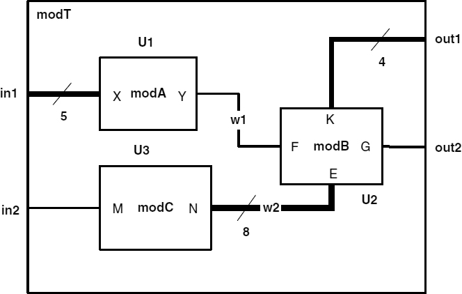
Figure 6.4 Block diagram of a module containing instances of other modules.
The names of the ports of each child module shown in Figure 6.4 are enclosed within the module's block; inputs enter on the left or bottom edge and outputs exit on the right or top edge.
Listing 6.2 shows the equivalent Verilog description of the block diagram of Figure 6.4.
1 module modT(input [4:0] in1,

2         input in2,

3         output [3:0] out1,

4         output out2);

5 wire [7:0] w2;

6 wire w1;


7 modA U1(.X(in1),. Y(w1));

8 modB U2(.F(w1),. E(w2),. K(out1),. G(out2));

9 modC U3(.M(in2),. N(w2));


10 endmodule
Listing 6.2 Verilog description for modT.
As was the case previously, the line numbers along the left-hand column are included for reference purposes; they do not form part of the module text. Lines 1 to 4 define the module header for modT: input in1 is a 5-bit port and output out1 is a 4-bit port; all remaining ports are single bit. Lines 5 and 6 declare two internal wires used to link modules modA and modC to modB.
The block structure shown in Figure 6.4 is effectively created by the module instantiation statements on lines 7, 8, and 9. Each line begins with the name of the module being instantiated; this is followed by a space and then the unique instance name (U1, U2, …).
In Verilog, there are two alternative ways of specifying module connectivity: the preferred method, known as explicit association, is used in Listing 6.2.
In this notation the ports of the child module are explicitly associated with particular signals by means of the ‘dot’ (.) notation, whereby the name of the signal being connected to the port is given in parentheses immediately after the selected port name, as shown below:
module-name instance-name(.port-name(net-name),…);
Explicit association has two important advantages over the second method that is sometimes used to define connectivity (discussed below):
- the connections may be listed in any order;
- the presence of both the port name and the name of the signal to which it is attached minimizes the possibility of errors.
The second method of defining module connectivity is known as positional association. In this notation, each port of the instantiated module is connected to the net occupying the corresponding position in the port list of the child module. For example, to instantiate module modA using positional association:
modA U1(in1, w1); //positional association
Clearly, positional association is less robust than explicit association due to the possibility of listing the connected signals in the wrong order. The Verilog compiler may not always report errors such as mismatches in the bit width or port direction caused by the wrong ports being connected to the wrong signals.
Occasionally, it is necessary to leave certain ports of a module unconnected. This can apply to both inputs and outputs. Regardless of whether explicit or positional association is used, unconnected ports are indicated by simply leaving blank the space where the connected signal name would normally appear. The two lines shown below illustrate the appearance of unconnected ports using the two alternative formats:
//output port ‘K’ is open circuit
modB U2(.F(w1),.E(w2),.K(),. G(out2));
//input port ‘E’ is unconnected
modB U4(w1,, out1, out2);
When an input is left unconnected, the Verilog simulator will force the corresponding port to take on the high-impedance value z.
As mentioned previously, Verilog uses two types of object to model signals in digital hardware:
- net or wire – must be continuously driven. The primary use is to model connections between continuous assignments and instantiations.
- reg – retains the last value that was assigned to it. Often (but not exclusively) used to represent storage elements.
Verilog imposes a set of rules regarding the nature of module ports and the type of object they can be connected to in a hierarchical design. Within the confines of a module, ports of direction input or inout are implicitly of type net (defaulting to wire). Module output ports can be of either the net or reg type.
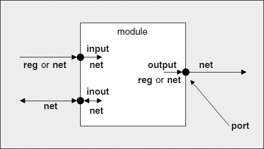
Figure 6.5 Illustration of Verilog port connectivity rules.
The output and inout ports of a module must be connected to nets at the next level up in the hierarchy. However, an input port may be driven by either a net- or a reg-type signal.
The above rules are summarized in Figure 6.5.
6.4 VERILOG HDL SIMULATION: A COMPLETE EXAMPLE
In this section, a complete example of a Verilog-HDL design, including a simulation test-fixture is presented. One of the key advantages of using an HDL, such as Verilog, is the ability to use the powerful features of the language to create the simulation environment for the design, as well as the design itself. This is the idea behind the so-called test-fixture (sometimes referred to as test-bench or test-module).
The main purpose of the test-fixture is to verify correct operation of the design; this can involve simply generating an input stimulus in order that the output responses may be observed, or more sophisticated techniques may be used to detect subtle design errors in more complex designs.
The principal advantage of the test-fixture results from the fact that it is written in the same standard language as the design and, therefore, provides the flexibility of simulation tool independence, being capable of running on any system that supports the IEEE standard Verilog.
Figure 6.6 shows the Verilog description and symbol for a single-bit binary adder [1]. The module FA uses the dataflow style of description to capture the behaviour of the logic; continuous assignments on lines 2 and 3 contain Boolean equations for the sum and carry outputs of the adder respectively. In terms of propagation delays, the adder module is ideal. Changes in any of the module inputs A, B and Ci will trigger execution of the two continuous assignments, causing the S and Cy outputs to be updated after one simulation cycle (delta).
The full adder module shown in Figure 6.6 could be described in a variety of alternative ways, ranging from primitive MOS switch circuitry at the lowest level, to high-level behavioural style. In this manner, Verilog supports the idea of top-down design, whereby a design is initially captured in an abstract manner to enable rapid verification of the design concept. The design can then be refined by changing its representation into a more detailed form, becoming closer to the eventual hardware technology being targeted.
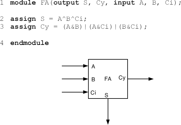
Figure 6.6 Verilog module and symbol for a binary full adder.
Having defined the single-bit adder module, Figure 6.7 illustrates how four full adders can be cascaded to form the so-called 4-bit ripple carry adder [1].
The module header (lines 1 and 2) for Add4 now defines outputs and inputs having a range of 3:0, i.e. 4 bits. The carry-input to the least significant bit and the carry-output from the most significant bit are the only single-bit ports.
The 4-bit adder is constructed using four module instantiations of the full adder module, having instance names fa0–fa3; these are situated on lines 4–11. The full adders are interconnected by the carry vector Cy (declared on line 3), as shown in the circuit below the listing, along with the external carry input Cin and the carry output Co, forming the ripple carry chain.
Notice the use in the listing in Figure 6.7 of explicit association and bit selection in defining the connectivity of the instantiated full adder modules. For example, individual bits of the A and B input vectors are connected to the corresponding full adder stage input ports by including the relevant bit number in square brackets after the name of the port, as shown below:
.A(Ain[1]) //FA port ‘A’ connects to bit-1 of input vector ‘Ain’
Although slightly longer, this technique is far clearer and leads to fewer errors being incorporated into the design.
Having constructed the 4-bit adder module, a test-fixture is used to verify the correctness of the design. Listing 6.3 and Figure 6.8 respectively show the Verilog listing and block diagram of a suitable test-fixture for the Add4 module.
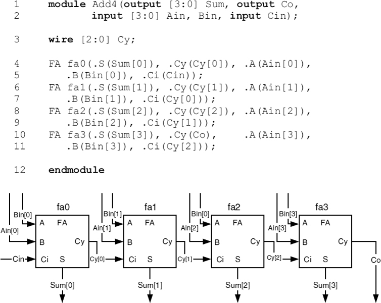
Figure 6.7 Verilog module and circuit for a 4-bit adder.
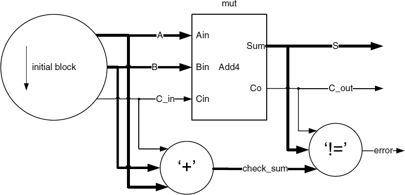
Figure 6.8 Block diagram of 4-bit adder test-module.
1 ‘timescale 1 ns/1 ns
2 module Test_Add4(); //test module - no ports needed

3 //input stimulus
4 reg[3:0] A, B;
5 reg C_in;

6 //wire to hold check sum and error flag
7 wire[4:0] check_sum;
8 wire error;

9 //output responses
10 wire[3:0] S;
11 wire C_out;

12 integer test;

13 initial //only allowed in test module - runs once only
14 begin
15    {A, B, C_in} = 9'b000000000;
16    #100; //wait for 100 time units
17    for(test = 0; test < 512; test = test + 1)
18    begin //apply all input values
19      {A, B, C_in} = test;
20      #100;
21    end
22    $stop; //system command - stops the simulation
23 end

24 //instantiate the module-under-test
25 Add4 mut(.Sum(S),. Co(C_out),. Ain(A),. Bin(B),
26       .Cin(C_in));

27 //add inputs using built-in ‘+’ operator
28 assign check_sum = A + B + C_in;
29 //compare with mut output
30 assign error = (check_sum ! = {C_out, S});
31
32 endmodule
Listing 6.3 Verilog test-module for 4-bit adder.
The block diagram of Figure 6.8 shows the structure of the test fixture. The conventional name given to the module being tested within the test fixture is module-under-test or mut, as shown above the symbol of the Add4 module in Figure 6.8. The Verilog test-fixture generates a set of test input stimuli for the adder inputs A, B and Cin by means of a behavioural construct known as an initial sequential block; this is represented by the circle to the left of the adder in Figure 6.8.
In order to perform a basic check that the 4-bit adder performs the correct operation, the built-in Verilog + operator is used to produce a 5-bit result named check_sum from the initial block outputs.
The check_sum value is compared with the outputs of the 4-bit adder using the built-in Verilog not-equal-to operator (!=). A diagnostic output named error indicates when there is a mismatch between the outputs of the adder and the result of performing the summation of the stimulus. In this manner, the test-fixture provides a simple single-bit indication of the validity of the Add4 module outputs.
The test-fixture Verilog description is given in Listing 6.3. This module makes use of several language constructs that have yet to be described. These new elements will be discussed briefly here and covered in more detail in Chapters 7 and 8.
The test-fixture module begins on line 1 with a so-called compiler directive. These special directives serve a similar purpose to the pre-processor directives found in the C/C++ languages; however, rather than beginning with the hash (#) symbol, Verilog uses the grave accent (`) character to indicate such a directive. The timescale directive on line 1 of Listing 6.3 defines a time scale and a time precision, the latter appearing after the ‘/’ character. In this example, both the time scale and precision are specified as 1 ns; this means that any time delay values appearing within the body of the module are interpreted by the simulator as representing a whole number of nanoseconds. The time precision can be set to as small a unit as the femtosecond (10−15s), thus allowing extremely precise timing simulation to be performed. In this example, there is no need for such precision.
The module header on line 2 indicates that the Test_Add4 module is a test-fixture module rather than a design module by virtue of the fact that there are no inputs and outputs. Note that the empty parentheses after the module name are optional and, therefore, can be omitted without incurring a syntax error; the terminating semicolon is always required, however.
Lines 4 and 5 declare the input stimulus signals that are connected to the inputs of the adder module. The keyword reg indicates that these signals must retain their value in between being updated by assignments within the sequential initial block starting on line 13.
The outputs of the module-under-test (lines 25 and 26) and the continuous assignments on lines 28 and 30 are continuously driven by these statements; therefore, they are declared as wires on lines 10, 11, 7 and 8 respectively.
The main part of the test-fixture is contained within the sequential initial block covering lines 13 to 23 in Listing 6.3. As stated previously, all signals that are assigned values by this block must be declared as type reg, in order that they retain the value last assigned to them during execution of the block.
The statements enclosed within the initial block execute sequentially and once only. This means that this type of block is only suitable for use in a test-fixture; it has no direct equivalent in terms of hardware.
Execution of the initial block starts at line 15, at a simulation time of 0 ns. The inputs are initialized to logic 0 using the following sequential statement:
{A, B, C_in} = 9'b000000000;
The inputs A, B and C_in are collectively assigned zeros by grouping them together using the concatenation operator { }.
Line 16 suspends execution of the sequential block for 100 ns; this allows the module-under-test to produce a response to the input stimulus. The hash (#) symbol represents a time delay in this particular context.
Following on from the initial time delay, lines 17 to 21 contain a for loop that iterates through the values 0 to 51110 using an integer variable test, the latter being declared on line 12. Note that integer is a reserved word that declares a signed whole number (usually 32 bits in length) that behaves in a similar manner to a reg, in that it, too, retains its value in between being updated by assignments within a sequential block.
for(test = 0; test < 512; test = test + 1)
begin //apply all input values
    {A, B, C_in} = test;
    #100;
end
The body of the for loop is a block enclosed between the keywords begin and end. The first statement (line 19) assigns the least significant 9 bits of the integer variable test to the aggregate of the inputs, this apparent mixing of different types either side of an assignment is permitted in Verilog.
The second statement within the for loop introduces a 100 ns delay before execution continues with the next iteration of the loop. In this manner, an exhaustive set of input combinations are applied to the adder inputs starting at ‘0000000002’ and ending at ‘1111111112’ (51110), each combination being applied for 100 ns.
The value of the loop variable test is incremented at the end of the loop and tested at the start of the loop; therefore, when it reaches 51210, the condition test < 512 becomes false and the loop terminates. An important point to note here is the possibility of a for loop being infinite, i.e. never terminating. This would occur if the loop variable test had been declared as a reg having a length of 9 bits rather than as a 32-bit integer. Since the range of values used within the loop and the number of inputs both correspond to a vector of length 9-bits, this may have seemed a logical course of action.
However, a problem occurs when the value of ‘test’ reaches ‘1111111112’.
Incrementing this value by one results in ‘0000000002’, due to the way in which a 9-bit unsigned binary number overflows. The terminating condition test < 512 can never be satisfied, since the 9-bit test value can never exceed 51110. Therefore, if a 9-bit reg had been used as the loop counter rather than an integer, the simulator would carry on applying the same sequence indefinitely while using up increasing amounts disk space to store the results!
One possible solution would be to declare test as a 10-bit reg; the spare bit allows the loop variable to reach the terminating value of ‘10000000002’.
Having applied an exhaustive set of input values, the simulation is automatically stopped by means of a very common Verilog system task on line 22, repeated below:
$stop;
System tasks are always preceded by the dollar ($) symbol and perform a wide variety of useful functions, ranging from performing detailed timing checks ($setup(), $hold(), etc.) to outputting simulation data to a file ($dumpvars, $dumpfile(“filename”)). The $stop system task is often used within a test-fixture to end the simulation run forcibly; examples showing the use of other system tasks will be covered in Chapters 7 and 8.
The description of the test-fixture shown in Listing 6.3 concludes with the continuous assignments on lines 28 and 30 and repeated below:
assign check_sum = A + B + C_in;
assign error = (check_sum !={C_out, S});
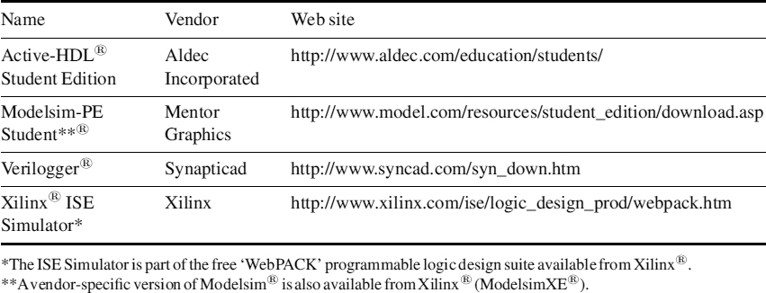
Table 6.1 Details of a few of the most popular Verilog simulator tools.
The above assignments generate a single-bit diagnostic signal named error which goes high if there is a discrepancy between the actual output of the 4-bit adder module and the theoretical value predicted by the built-in addition operator. Although this may seem a little unnecessary, given the simplicity of the design, it hopefully illustrates the potential advantage of using the expressive power of the Verilog language to aid in the verification of a more complex design.
Simulation of the 4-bit adder module and associated test-fixture requires a Verilog-2001 [9] compatible simulation tool. There are several excellent Verilog simulators available from a variety of vendors. Table 6.1 contains details of a few of the most popular tools.
Regardless of which of the simulators in Table 6.1 is used, the process of simulation starts with the creation of the Verilog sources. It is normal practice to store each individual module's textual description in aunique ASCII text file (usually named ‘module-name.v’). Most simulation tools include a context-sensitive text editor to aid in the creation of the source files; such an editor will include colour-coded keyword highlighting, line numbering and automatic indentation and formatting of the language statements. All the previously mentioned features help the designer to understand and maintain complex designs.
Most simulators make use of the concept of a project. This is essentially a repository for all of the Verilog files used in the design. Once written, the source files are added to the project prior to the next step, i.e. compilation. The process of compilation is similar in many ways to that used in other high-level language development systems: the objective is to build an executable model suitable for loading into the simulation kernel, once any syntax errors have been corrected.
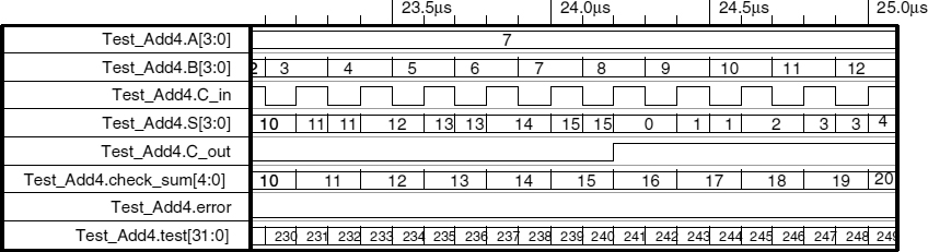
Figure 6.9 Partial simulation result for 4-bit adder test-module.
All Verilog simulators provide a graphical output in the form of timing waveforms. Figure 6.9 shows the partial result from running the simulation of the Test_Add4 test-fixture module given in Listing 6.3.
REFERENCES
1. Wakerly J.F. Digital Design: Principles and Practices, 4th edition. New Jersey: Pearson Education, 2006.
2. www.systemc.org [2007 October].
3. www.systemverilog.org [2007 October].
4. www.verilog.com [2007 October]. (Links to IEEE Standards site and other Verilog information.)
5. www.accellera.org/home [2007 October].
6. www.adacore.com/home/ada_answers/ada_overview [2007 October].
7. www.synopsys.com/products/logic/design_compiler.html [2007 October].
8. Weste N.H.E., Eshraghian K. Principles of CMOS VLSI Design. Addison Wesley, 1993; Section 6.2.
9. Ciletti M.D. Advanced Digital Design with the Verilog HDL. New Jersey: Pearson Education, 2003; Appendix I – Verilog-2001.
In addition to the references listed, there are a considerable number of excellent internet sites containing tutorial and reference material on Verilog; many of these can be located using a standard internet search engine by entering the keyword ‘Verilog’