
7
Elements of Verilog HDL
This chapter introduces the basic lexical elements of the Verilog HDL. In common with other high-level languages, Verilog defines a set of types, operators and constructs that make up the vocabulary of the language. Emphasis is placed on those aspects of the language that support the description of synthesizable combinatorial and sequential logic.
7.1 BUILT-IN PRIMITIVES AND TYPES
7.1.1 Verilog Types
As mentioned in Chapter 6, Verilog makes use of two basic types: nets and registers. Generally, nets are used to establish connectivity and registers are used to store information, although the latter does not always imply the presence of sequential logic.
Within each category there exist several variants; these are listed in Table 7.1. All of the type names, listed in Table 7.1, are Verilog reserved words; the most commonly used types are shown in bold.
Along with the basic interconnection net type wire, two additional predefined nets are provided to model power supply connections: supply0 and supply1.
These special nets possess the so-called ‘supply’ drive strength (the strongest; it cannot be overridden by another value) and are used whenever it is necessary to tie input ports to logic 0 or logic 1. The following snippet of Verilog shows how to declare and use power supply nets:
module …

supply0 gnd;
supply1 vdd;
  nand g1(y, a, b, vdd); //tie one input of nand gate high

endmodule
The power supply nets are also useful when using Verilog to describe switch-level MOS circuits. However, the Verilog switch-level primitives [1] (nmos, pmos, cmos, etc.) are not generally supported by synthesis tools; therefore, we will not pursue this area any further here.
| Nets (connections) | Registers (storage) |
| wire | |
| tri | |
| supply0 | reg |
| supply1 | integer |
| wand | real |
| wor | time |
| tri0 | realtime |
| tri1 | |
| triand | |
| trireg | |
| trior |
Of the remaining types of net shown in the left-hand column of Table 7.1, most are used to model advanced net types that are not supported by synthesis tools; the one exception is the net type tri. This net is exactly equivalent to the wire type of net and is included mainly to improve clarity. Both wire and tri nets can be driven by multiple sources (continuous assignments, primitives or module instantiations) and can, therefore, be in the high-impedance state (z) when none of the drivers are forcing a valid logic level. The net type tri can be used instead of wire to indicate that the net spends a significant amount of the time in the high-impedance state.
Nets such as wire and tri cannot be assigned an initial value as part of their declaration; the default value of these nets at the start of a simulation is high impedance (z).
The handling of multiple drivers and high-impedance states is built in to the Verilog HDL, unlike some other HDLs, where additional IEEE-defined packages are required to define types and supporting functions for this purpose.
The right-hand column of Table 7.1 lists the register types provided by Verilog; these have the ability to retain a value in-between being updated by a sequential assignment and, therefore, are used exclusively inside sequential blocks. The two most commonly used register variables are reg and integer; the remaining types are generally not supported by synthesis tools and so will not be discussed further.
There are some important differences between the reg and integer types that result in the reg variable being the preferred type in many situations.
A reg can be declared as a 1-bit object (i.e. no size range is specified) or as a vector, as shown by the following examples:
reg a, b; //single-bit register variables
reg [7:0] busa; //an 8-bit register variable
As shown above, a reg can be declared to be of any required size; it is not limited by the word size of the host processor.
An integer, on the other hand, cannot normally be declared to be of a specified size; it takes on the default size of the host machine, usually 32 or 64 bits.
The other difference between the integer and reg types relates to the way they are handled in arithmetic expressions. An integer is stored as a two's complement signed number and is handled in arithmetic expressions in the same way, i.e. as a signed quantity (provided that all operands in the expression are also signed). In contrast, a reg variable is by default an unsigned quantity.
If it is necessary to perform signed two's complement arithmetic on regs or wires, then they can be qualified as being signed when they are declared. This removes the host-dependent word length limit imposed by the use of the integer type:
reg signed [63:0] sig1; //a 64-bit signed reg
wire signed [15:0] sig2; //a 16-bit signed wire
…
The use of the keyword signed to qualify a signal as being both positive and negative also applies to module port declarations, as shown in the module header below:
module mod1(output reg signed [11:0] dataout,
         input signed [7:0] datain,
         output signed [31:0] dataout2);
…
Finally, both the integer and reg types can be assigned initial values as part of their declarations, and in the case of the reg this can form part of the module port declaration, as shown below:
module mod1(output reg clock = 0,
         input [7:0] datain = 8′hFF,
         output [31:0] dataout2 = 0);
integer i = 3;
…
The differences discussed above mean that the reg and integer variables have different scopes of application in Verilog descriptions. Generally, reg variables are used to model actual hardware registers, such as counters, state registers and data-path registers, whereas integer variables are used for the computational aspects of a description, such as loop counting. The example in Listing 7.1 shows the use of the two types of register variable.
The Verilog code shown describes a 16-bit synchronous binary up-counter. The module makes use of two always sequential blocks – a detailed description of sequential blocks is given in the Chapter 8.
The first sequential block, spanning lines 5 to 11 of Listing 7.1, describes a set of flip flops that are triggered by the positive edges (logic 0 to logic 1) of the ‘clock’ input.
The state of the flip flops is collectively stored in the 16-bit reg-type output signal named q, declared within the module header in line 2. Another 16-bit reg-type signal, named t, is declared in line 3. This vector is the output of a combinational circuit described by the sequential block spanning lines 12 to 20. This illustrates the point that a reg-type signal does not always represent sequential logic, being necessary wherever a signal must retain the value last assigned to it by statements within a sequential block. The always block starting on line 12 responds to changes in the outputs of the flip flops q and updates the values of t accordingly. The updated values of the t vector then determine the next values of the q outputs at the subsequent positive edge of the ‘clock’ input.
1 module longcnt (input clock, reset, output reg [15:0] q);
2
3 reg [15:0] t; //flip-flop outputs and inputs
4 //sequential logic
5 always @ (posedge clock)
6 begin
7        if (reset)
8           q <= 16'b0;
9        else
10          q <= q ^ t;
11 end

12 always @(q) //combinational logic
13 begin: t_block
14      integer i; //integer used as loop-counter
15      for (i = 0; i < 16; i = i + 1)
16          if (i == 0)
17             t[i] = 1'b1;
18          else
19             t[i] = q[i − 1] & t[i − 1];
20 end
21 endmodule
Listing 7.1 Use of Verilog types reg and integer.
The second sequential block (lines 12–20) is referred to as a named block, due to the presence of the label t_block after the colon on line 13. Naming a block in this manner allows the use of local declarations of both regs and integers for use inside the confines of the block (between begin and end). In this example, the integer i is used by the for loop spanning lines 15–19, to process each bit of the 16-bit reg t, such that apart from t[0], which is always assigned a logic 1, the ith bit of t(t[i]) is assigned the logical AND (&) of the (i − 1 )th bits of q and t. The sequential always block starting on line 12 describes the iterative logic required to implement a synchronous binary ascending counter.

Figure 7.1 Block diagram of module longcnt.
Figure 7.1 shows the structure of the longcnt module given in Listing 7.1. Simulation of a 4-bit version of the binary counter module longcnt results in the waveforms shown in Figure 7.2. The waveforms in Figure 7.2 clearly show the q outputs counting up in ascending binary, along with the corresponding t vector pulses causing the q output bits to ‘toggle’ state at the appropriate times. For example, when the q output is ‘01112’, the t vector is ‘11112’ and so all of the output bits toggle (change state) on the next positive edge of ‘clock’.
7.1.2 Verilog Logic and Numeric Values
Each individual bit of a Verilog HDL reg or wire can take on any one of the four values listed in Table 7.2. Verilog also provides built-in modelling of signal strength; however, this feature is generally not applicable to synthesis and, therefore, we will not cover it here.
Of the four values listed in Table 7.2, logic 0 and logic 1 correspond to Boolean false and true respectively. In fact, any nonzero value is effectively true in Verilog, as it is in the C/C++ programming languages. Relational operators all result in a 1-bit result indicating whether the comparison is true (1) or false (0).

Figure 7.2 Simulation results for module longcnt (4-bit version)
| Logic value | Interpretation |
| 0 | Logic 0 or false |
| 1 | Logic 1 or true |
| x | Unknown (or don't care) |
| z | High impedance |
Two meta-logical values are also defined. These model unknown states (x) and high impedance (z); the x is also used to represent ‘don't care’ conditions in certain circumstances. At the start of a simulation, at time zero, all regs are initialized to the unknown state x, unless they have been explicitly given an initial value at the point of declaration. On the other hand, wires are always initialized to the undriven state z.
Once a simulation has commenced, all regs and wires should normally take on meaningful numeric values or high impedance; the presence of x usually indicates a problem with the behaviour or structure of the design.
Occasionally, the unknown value x is deliberately assigned to a signal as part of the description of the module. In this case, the x indicates a so-called don't care condition, which is used during the logic minimization process underlying logic synthesis.
Verilog provides a set of built-in pre-defined logic gates, these primitive elements respond to unknown and high-impedance inputs in a sensible manner. Figure 7.3 shows the simulation results for a very simple two-input AND gate module using the built-in and primitive. The simulation waveforms show how the output of the module below responds when its inputs are driven by x and z states.
1 module valuedemo(output y, input a, b) ;
2 and g1(y, a, b);
3 endmodule
Referring to the waveforms in Figure 7.3, during the period 0–250 ns the and gate output y responds as expected to each combination of inputs a and b. At time 250 ns, the a input is driven to the z state (indicated by the dotted line) and the gate outputs an x (shaded regions) between 300 and 350 ns, since the logical AND of logic 1 and z is undefined. Similarly, during the interval 400–450 ns, the x on the b input also causes the output y to be an x.

Figure 7.3 The and gate response to x and z.
However, during the intervals 350–400 ns and 250–300 ns, one of the inputs is low, thus causing y to go low. This is due to the fact that anything logically ANDed with a logic 0 results in logic 0.
7.1.3 Specifying Values
There are two types of number used in Verilog HDL: sized and unsized. The format of a sized number is
<size>'<base><number>.
Both the <size> and <base> fields are optional; if left out, the number is taken to be in decimal format and the size is implied from the variable to which the number is being assigned.
The <size> is a decimal number specifying the length of the number in terms of binary bits; <base> can be any one of the following:
| binary | b or B |
| hexadecimal | h or H |
| decimal (default) | d or D |
| octal | o or O |
The actual value of the number is specified using combinations of the digits from the set ![]() 0, 1, 2, 3, 4, 5, 6, 7, 8, 9, A, B, C, D, E, F
0, 1, 2, 3, 4, 5, 6, 7, 8, 9, A, B, C, D, E, F![]() . Hexadecimal numbers may use all of these digits; however, binary, octal and decimal are restricted to the subsets
. Hexadecimal numbers may use all of these digits; however, binary, octal and decimal are restricted to the subsets ![]() 0, 1
0, 1![]() ,
, ![]() 0–7
0–7![]() and
and ![]() 0–9
0–9![]() respectively. Below, are some examples of literal values written using the format discussed above:
respectively. Below, are some examples of literal values written using the format discussed above:
4'b0101 //4-bit binary number
12'hefd //12-bit hex number
16'd245 //16-bit decimal number
1'b0, 1'b1 //logic-0 and logic-1
Generally, it is not necessary to specify the size of a number being assigned to an integer-type variable, since such objects are unsized (commonly occupying 32 bits or 64 bits, depending upon the platform).
The literals x and z (unknown and high impedance) may be used in binary-, hexadecimal- and octal-based literal values. An x or z sets 4 bits in a hex number, 3 bits in an octal number and 1 bit in a binary number.
Furthermore, if the most-significant digit of a value is 0, z or x, then the number is automatically extended using the same digit so that the upper bits are identical.
Below, are some examples of literal values containing the meta-logical values x and z:
12'h13x //12-bit hex number ‘00010011xxxx’ in binary
8'hx //8-bit hex number ‘xxxxxxxx’ in binary
16'bz //16-bit binary number ‘zzzzzzzzzzzzzzzz’
11'b0 //11-bit binary number ‘00000000000’
As shown above, the single-bit binary states of logic 0 and logic 1 are usually written in the following manner:
1'b0 //logic-0
1'b1 //logic-1
Of course, the single decimal digits 0 and 1 can also be used in place of the above. As mentioned previously, in Verilog, the values 1'b0 and 1'b1 correspond to the Boolean values ‘false’ and ‘true’ respectively.
7.1.4 Verilog HDL Primitive Gates
The Verilog HDL provides a comprehensive set of built-in primitive logic and three-state gates for use in creating gate-level descriptions of digital circuits. These elements are all synthesizable; however, they are more often used in the output gate-level Verilog net-list produced by a synthesis tool.
Figures 7.4 and 7.5 show the symbolic representation and Verilog format for each of the primitives [1]. The use of the primitive gates is fairly self-explanatory; the basic logic gates, such as AND, OR, etc., all have single-bit outputs but allow any number of inputs (Figure 7.4 shows two-input gates only). The Buffer and NOT gates allow multiple outputs and have a single input.
The three-state gates all have three terminals: output, input and control. The state of the control terminal determines whether or not the buffer is outputting a high-impedance state or not.
For all gate primitives, the output port must be connected to a net, usually a wire, but the inputs may be connected to nets or register-type variables.
An optional delay may be specified in between the gate primitive name and the instance label; these can take the form of simple propagation delays or contain separate values for rise-time, fall-time and turnoff-time delays [1], as shown by the examples below:
//AND gate with output rise-time of 10 time units
//and fall-time of 20 time units
and #(10, 20) g1 (t3, t1, a);

//three-state buffer with output rise-time of 15 time unit,
//fall-time of 25 time units
//and turn-off delay time of 20 time units
bufif1 #(15, 25, 20) b1 (dout, din, c1);
Figure 7.6 shows a simple example of a gate-level Verilog description making use of the built-in primitives; each primitive gate instance occupies a single line from numbers 4 to 8 inclusive. A single propagation delay value of 10 ns precedes the gate instance name; this means that changes at the input of a gate are reflected at the output after this delay, regardless of whether the output is rising or falling. The actual units of time to be used during the simulation are defined using the timescale compiler directive; this immediately precedes the module to which it applies, as shown in line 1 in Figure 7.6.
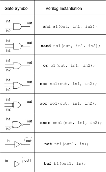
Figure 7.4 Verilog primitive logic gates.

Figure 7.5 Verilog primitive three-state gates

Figure 7.6 Gate-level logic circuit and Verilog description.
Gate delays are inertial, meaning that input pulses which have a duration of less than or equal to the gate delay do not produce a response at the output of the gate, i.e. the gate's inertia is not overcome by the input change. This behaviour mirrors that of real logic gates.
Gate delays such as those used in Figure 7.6 may be useful in estimating the performance of logic circuits where the propagation delays are well established, e.g. in the model of a TTL discrete logic device. However, Verilog HDL descriptions intended to be used as the input to logic synthesis software tools generally do not contain any propagation delay values, since these are ignored by such tools.
7.2 OPERATORS AND EXPRESSIONS
The Verilog HDL provides a powerful set of operators for use in digital hardware modelling. The full set of Verilog operators is shown in Table 7.3. The table is split into four columns, containing (from left to right) the category of the operator, the symbol used in the language for the operator, the description of the operator and the number of operands used by the operator.
Inspection of Table 7.3 reveals the similarity between the Verilog operators and those of the C/C++ languages. There are, however, one or two important differences and enhancements provided by Verilog in comparison with C/C++. The main differences between the C-based languages and Verilog, in terms of operators, are summarized overleaf:

- Verilog provides a powerful set of unary logical operators (so-called reduction operators) that operate on all of the bits within a single word.
- Additional ‘case’ equality/inequality operators are provided to handle high-impedance (z) and unknown (x) values.
- The curly braces ‘{’ and ‘}’ are used in the concatenation and replication operators instead of block delimiters (Verilog uses begin … end for this).
The operators listed in Table 7.3 are combined with operands to form an expression that can appear on the right hand side of a continuous assignment statement or within a sequential block.

Figure 7.7 Exclusive OR of part-selects.
The operands used to form an expression can be any combination of wires, regs and integers; but, depending on whether the expression is being used by a continuous assignment or a sequential block, the target must be either a wire or a reg respectively.
In the case of multi-bit objects (buses), an operand can be the whole object (referenced by the name of the object), part-select (a subset of the bits within a multi-bit bus) or individual bit, as illustrated by the following examples.
Given the following declarations, Figures 7.7–7.10 show a selection of example continuous assignments and the corresponding logic circuits.
wire   [7:0] a, b; //8-bit wire
wire   [3:0] c;   //4-bit wire
wire   d;  //1-bit wire
Figure 7.7 illustrates the use of the bitwise exclusive OR operator on two 4-bit operands. As shown by the logic circuit in Figure 7.7, part-selects [3:0] of the two 8-bit wires, a and b, are processed bit-by-bit to produce the output c.
Individual bits of a wire or reg are accessed by means of the bit-select (square brackets [ ]) operator. Figure 7.8 shows the continuous assignment statement and logic for an AND gate with an inverted input.

Figure 7.8 Logical AND of bit-selects.

Figure 7.9 Reduction NOR operator.
The bit-wise reduction operators, shown in Table 7.3, are unique to Verilog HDL. They provide a convenient method for processing all of the bits within a single multi-bit operand. Figure 7.9 shows the use of the reduction-NOR operator. This operator collapses all of the bits within the operand a down to a single bit by ORing them together; the result of the reduction is then inverted, as shown by the equivalent expression below:
assign d = ~(a[7] |a[6] |a[5] |a[4] |a[3] |a[2] |a[1] |a[0]);
The target d of the continuous assignment statement in Figure 7.9 will be logic 1 if all 8 bits of a are logic 0, otherwise d is assigned logic 0. All of the reduction operators act on one operand positioned to the right of the operator. Those that are inverting, such as reduction NOR (~|) and reduction NAND (~&), combine all of the bits of the operand using bitwise OR or bitwise AND prior to inverting the single-bit result. The bitwise reduction operators provide a convenient means of performing multi-bit logical operations without the need to instantiate a primitive gate. Finally, if any bit or bits within the operand are high impedance (z), the result is generated as if the corresponding bits were unknown (x).
The last example, shown in Figure 7.10, illustrates the use of the conditional operator (? :) to describe a set of four 2-to-1 multiplexers, the true expression a[3:0] is assigned to c when the control expression, in this case d, is equal to 1'b1. When the single-bit signal d is equal to logic 0(1'b0), the target c is assigned the false expression a[7:4].
The unsigned shift operators (![]() ,
, ![]() in Table 7.3) shuffle the bits within a multi-bit wire or reg by a number of bit positions specified by the second operand. These operators shift logic 0s into the vacant bit positions; because of this, care must be taken when shifting two's complement (signed) numbers. If a negative two's complement number is shifted right using the ‘
in Table 7.3) shuffle the bits within a multi-bit wire or reg by a number of bit positions specified by the second operand. These operators shift logic 0s into the vacant bit positions; because of this, care must be taken when shifting two's complement (signed) numbers. If a negative two's complement number is shifted right using the ‘![]() ’ operator, then the sign bit is changed from a 1 to a 0, changing the polarity of the number from negative to positive.
’ operator, then the sign bit is changed from a 1 to a 0, changing the polarity of the number from negative to positive.
Right-shifting of two's complement numbers can be achieved by means of the ‘shift right signed’ (![]() ) operator (provided the wire or reg is declared as signed) or by using the replication/concatenation operators (see later).
) operator (provided the wire or reg is declared as signed) or by using the replication/concatenation operators (see later).
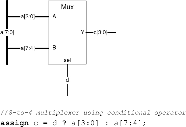
Figure 7.10 An 8-to-4 multiplexer.
The following assignments illustrate the use of the unsigned shift operators:
//declare and initialize X
reg [3:0] X = 4'b1100;
Y = X » 1; //Result is 4'b0110
Y = X « 1; //Result is 4'b1000
Y = X » 2; //Result is 4'b0011
Verilog supports the use of arithmetic operations on multi-bit reg and wire objects as well as integers; this is very useful when using the language to describe hardware such as counters (+, − and %) and digital signal processing systems (* and /).
With the exception of type integer, the arithmetic and comparison operators treat objects of these types as unsigned by default. However, as discussed in Section 7.1, regs and wires (as well as module ports) can be qualified as being signed. In general, Verilog performs signed arithmetic only if all of the operands in an expression are signed; if an operand involved in a particular expression is unsigned, then Verilog provides the system function $signed() to perform the conversion if required (an additional system function named $unsigned() performs the reverse conversion).
Listing 7.2 illustrates the use of the multiply, divide and shifting operators on signed and unsigned values. As always, the presence of line numbers along the left-hand column is for reference purposes only.
//test module to demonstrate signed/unsigned arithmetic
1 module test_v2001_ops();
2 reg [7:0] a = 8'b01101111; //unsigned value
3 reg signed [3:0] d = 4'b0011; //signed value
4 reg signed [7:0] b = 8'b10010110; //signed value
5 reg signed [15:0] c; //signed value
6 initial
7 begin
8    c = a * b; // unsigned value * signed value
9    #100;
10   c = $signed (a) * b; // signed value * signed value
11   #100;
12   c = b / d; // signed value ÷ signed value
13   #100;
14   b = b
15   #100;
16   d = d « 2; //shift left logically
17   #100;
18   c = b * d; // signed value * signed value
19   #100;
20   $stop;
21 end
22 endmodule

Listing 7.2 Signed and unsigned arithmetic.
The table shown below the Verilog source listing in Listing 7.2 shows the results of simulating the module test_v2001_ops(); the values of a, b, c and d are listed in decimal.
The statements contained within the initial sequential block starting on line 6 execute from top to bottom in the order that they are written; the final $stop statement, at line 20, causes the simulation to terminate. The result of each statement is given along with the corresponding line number in the table in Listing 7.2.
The statement on line 8 assigns the product of an unsigned and a signed value to a signed value. The unsigned result of 16 65010 is due to the fact that one of the operands is unsigned and, therefore, the other operand is also handled as if it were unsigned, i.e. 15010 rather than – 10610.
The statement on line 10 converts the unsigned operand a to a signed value before multiplying it by another signed value; hence, all of the operands are signed and the result, therefore, is signed (−11 76610).
The statement on line 12 divides a signed value (−10610) by another signed value (+310), giving a signed result (−3510). The result is truncated due to integer division.
Line 14 is a signed right-shift, or arithmetic right-shift (![]() operator). In this case, the sign-bit (most significant bit (MSB)) is replicated four times and occupies the leftmost bits, effectively dividing the number by 1610 while maintaining the correct sign. In binary, the result is ‘111110012’, which is −710.
operator). In this case, the sign-bit (most significant bit (MSB)) is replicated four times and occupies the leftmost bits, effectively dividing the number by 1610 while maintaining the correct sign. In binary, the result is ‘111110012’, which is −710.
A logical shift-left (![]() ) is performed on a signed number on line 16. Logical shifts always insert zeros in the vacant spaces and so the result is ‘11002’, or −410.
) is performed on a signed number on line 16. Logical shifts always insert zeros in the vacant spaces and so the result is ‘11002’, or −410.
Finally, on line 18, two negative signed numbers are multiplied to produce a positive result.
The use of the keyword signed and the system functions $signed and $unsigned are only appropriate if the numbers being processed are two's complement values that represent bipolar quantities. The emphasis in this book is on the design of FSMs where the signals are generally either single-bit or multi-bit values used to represent a machine state. For this reason, the discussion presented above on signed arithmetic will not be developed further.
The presence of the meta-logical values z or x in a reg or wire being used in an arithmetic expression results in the whole expression being unknown, as illustrated by the following example:
//assigning values to two 4-bit objects
in1 = 4'b101x;
in2 = 4'b0110;
sum = in1 + in2; //sum = 4′bxxxx due to ‘x’ in in1
Figure 7.11 shows a further example of the use of the Verilog bitwise logical operators. The continuous assignment statement on lines 4 to 7 makes use of the AND(&), NOT(~) and OR(|) operators; note that there is no need to include parentheses around the inverted inputs, since the NOT operator (~) has a higher precedence than the AND (&) operator. However, the parentheses around the ANDed terms are required, since the ‘&’ and ‘|’ operators have the same precedence.
Figure 7.12 shows an alternative way of describing the same logic described by Figure 7.11. Here, a nested conditional operator is used to select one of four inputs i0-i3, under the control of a 2-bit input s1, s0 and assign it to the output port named out.
There is no limit to the degree of nesting that can be used with the conditional operator, other than that imposed by the requirement to maintain a certain degree of readability.
The listing in Figure 7.13 shows another use of the conditional operator. Here, it is used on line 3 to describe a so-called ‘three-state buffer’ as an alternative to using eight instantiations of the built-in primitive bufif1 (see Figure 7.5).
When the enable input is at logic 1, the Dataout port is driven by the value applied to Datain; on the other hand, when the enable input is at logic 0, the Dataout port is effectively undriven, being assigned the value ‘zzzzzzzz’.
In addition to ports of direction input and output, Verilog provides for ports that allow two-way communication by means of the inout keyword. Figure 7.14 illustrates a simple bidirectional interface making use of an inout port. It is necessary to drive bidirectional ports to the high-impedance state when they are acting as an input, hence the inclusion of the 8-bit three-state buffer on line 3. The Verilog simulator makes use of a built-in resolution mechanism to predict correctly the value of a wire that is subject to multiple drivers. In the current example, the bidirectional port Databi can be driven to a logic 0 or logic 1 by an external signal; hence, it has two drivers. The presence of a logic level on the Databi port will override the high-impedance value being assigned to it by line 3; hence, Datain will take on the value of the incoming data applied to Databi as a result of the continuous assignment on line 4.
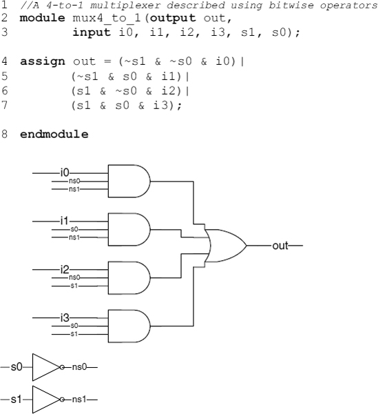
Figure 7.11 A 4-to-1 multiplexer described using bitwise operators.
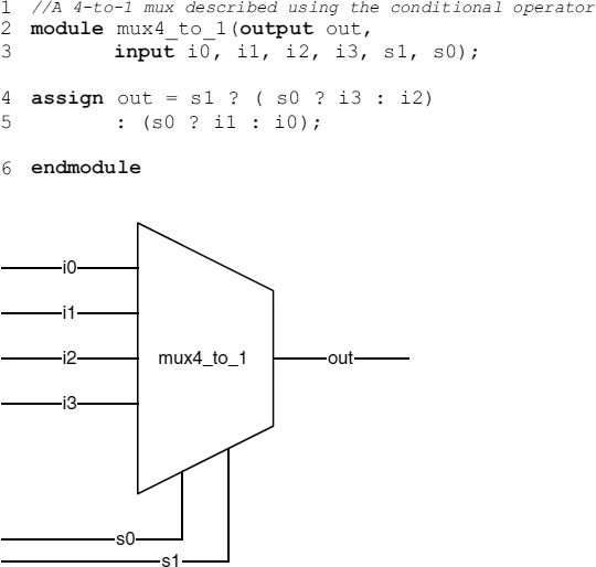
Figure 7.12 A 4-to-1 multiplexer described using nested conditional operators.

Figure 7.13 An 8-bit three-state buffer.
The simple combinational logic example given in Figure 7.15 illustrates the use of the logical OR operator (||) and the equality operator (==). The module describes a three-input majority voter that outputs a logic 1 when two or more of the inputs is at logic 1.
On line 4, the individual input bits are grouped together to form a 3-bit value on wire abc. The concatenation operator ({ }) is used to join any number of individual 1-bit or multi-bit wires or regs together into one bus signal. Line 4 illustrates the use of the combined wire declaration and continuous assignment in a single statement.

Figure 7.14 A bidirectional bus interface.

Figure 7.15 A three-input majority voter.
The continuous assignment on lines 5 to 8 in Figure 7.15 incorporates a delay, such that any input change is reflected at the output after a 10 ns delay. This represents one method of modelling propagation delays in modules that do not instantiate primitive gates.
The expression on the right-hand side of the assignment operator on line 5 makes use of the logical OR operator (||) rather than the bitwise OR operator (|). In this example, it makes no difference which operator is used, but occasionally the choice between bitwise and object-wise is important, since the latter is based on the concept of Boolean true and false. In Verilog, any bit pattern other than all zeros is considered to be true; consider the following example:
wire[3:0] a = 4'b1010; //true
wire[3:0] b = 4'b0101; //true
wire[3:0] c = a&b; //bit-wise result is 4′b0000 (false)
wire d = a&&b; //logical result is 1′b1 (true)
Verilog-HDL provides a full set of relational operators, such as greater than, less than and greater than or equal to, as shown in Table 7.3. The following example, given in Figure 7.16, illustrates the use of these operators in the description of a memory address decoder.
The purpose of the module shown in Figure 7.16 is to activate one of four active-low ‘chip select’ outputs Csbar[3:0], depending upon what particular range of hexadecimal address values is present on the 16-bit input address. Such a decoder is often used to implement the memory map of a microprocessor-based system.
Each of the continuous assignments on lines 4, 6, 8 and 10 responds to changes in the value of the input Address. For example, Csbar[2] is driven to logic 0 when Address changes to a hexadecimal value within the range 150016 to 16FF16 inclusive.
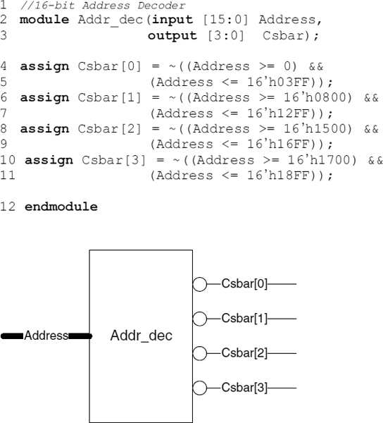
Figure 7.16 Memory address decoder using the relational operators.
Another example of the use of the relational operators is shown in Figure 7.17. This shows the Verilog description of a 4-bit magnitude comparator.
The module given in Figure 7.17 makes use of the relational and equality operators, along with logical operators, to form the logical expressions contained within the conditional operators on the right-hand side of the continuous assignments on lines 5 and 7. Note the careful use of parentheses in the test expression contained within line 7 for example:
((a > b) || ( (a == b) && (agtbin == 1'b1))) ?
The parentheses force the evaluation of the logical AND expression before the logical OR expression, the result of the whole expression is logical ‘true’ or ‘false’, i.e. 1'b1 or 1'b0. The result of the Boolean condition selects between logic 1 and logic 0 and assigns this value to the agtbout output. The expression preceding the question mark (?) on lines 7 and 8 could have been used on its own to produce the correct output on port agtbout; the conditional operator is used purely to illustrate how a variety of operators can be mixed in one expression.
The expression used on the right-hand side of the continuous assignment on line 9, shown below, makes use of the bitwise logical operators to illustrate that, in this case, the outcome is exactly the same as that which would be produced by the logical operators:
altbout = (a < b) | ((a == b) & altbin);
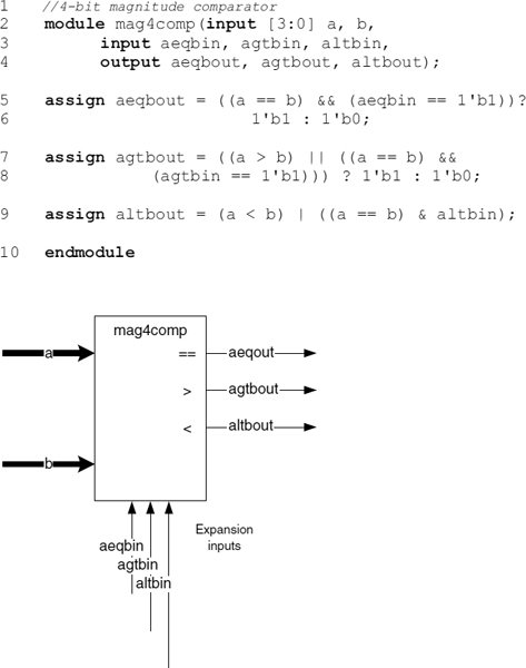
Figure 7.17 A 4-bit magnitude comparator.
The relational and logical operators used in the above examples will always produce a result of either logic 0 or logic 1 provided the operands being compared do not contain unknown (x) or high-impedance (z) values in any bit position. In the event that an operand does contain a meta-logical value, these operators will generate an unknown result (x), as illustrated by the examples below:
reg[3:0] A = 4'b1010;
reg[3:0] B = 4'b1101;
reg[3:0] C = 4'b1xxx;

A <= B //Evaluates to logic-1
A > B //Evaluates to logic-0
A && B //Evaluates to logic-1
C == B //Evaluates to x
A < C //Evaluates to x
C || B //Evaluates to x
In certain situations, such as in simulation test-fixtures, it may be necessary to detect when a module outputs an unknown or high-impedance value; hence, there exists a need to be able to compare values that contain x and z.
Verilog HDL provides the so-called case-equality operators (‘===’ and ‘!==’) for this purpose. These comparison operators compare xs and zs, as well as 0s and 1s; the result is always 0 or 1. Consider the following examples:
reg[3:0] K = 4'b1xxz;
reg[3:0] M = 4'b1xxz;
reg[3:0] N = 4'b1xxx;

K === M //exact match, evaluates to logic-1
K === N //1-bit mismatch, evaluates to logic-0
M !== N //Evaluates to logic-1
Each of the three reg signals declared above is initialized to an unknown value; the three comparisons that follow yield 1s and 0s, since all four possible values (0, 1, x, z) are considered when performing the case-equality and case-inequality bit-by-bit comparisons.
The last operators in Table 7.3 to consider are the replication and concatenation operators; both make use of the curly-brace symbol ({ }) commonly used to denote a begin…end block in the C-based programming languages.
The concatenation ({ }) operator is used to append, or join together, multiple operands to form longer objects. All of the individual operands being combined must have a defined size, in terms of the number of bits. Any combination of whole objects, part-selects or bit-selects may be concatenated, and the operator may be used on either or both sides of an assignment. The assignments shown below illustrate the use of the concatenation operator:
// A = 1'b1, B = 2'b00, C = 3'b110
Y = {A, B}; //Y is 3'b100
Z = {C, B, 4'b0000}; //Z is 9'b110000000
W = {A, B[0], C[1]}; //W is 3'b101
The following Verilog statements demonstrate the use of the concatenation operator on the left-hand side (target) of an assignment. In this case, the ‘carry out’ wire c_out occupies the MSB of the 5-bit result of adding two 4-bit numbers and a ‘carry input’:
wire[3:0] a, b, sum;
wire c_in, c_out;

//target is 5-bits long [4:0]
{c_out, sum} = a + b + c_in;
The replication operator can be used on its own or combined with the concatenation operator. The operator uses a replication constant to specify how many times to replicate an expression. If j is the expression being replicated and k is the replication constant, then the format of the replication operator is as follows:
{k{j}}
The following assignments illustrate the use of the replication operator.
//a = 1'b1, b = 2'b00, c = 2'b10

//Replication only
Y = {4{a}} //Y is 4'b1111

//Replication and concatenation
Y = {4{a}, 2{b}} //Y is 8'b11110000
Y = {3{c}, 2{1'b1}} //Y is 8'b10101011
One possible use of replication is to extend the sign-bit of a two's complement signed number, as shown below:
//a two's comp value wire[7:0] data = 8'b11001010; //arithmetic right shift by 2 places //data is 8'b11110010
assign data = {3{data[7]}, data[6:2]};
The above operation could have been carried out using the arithmetic shift right operator ‘![]() ’; however, the wire declaration for data would have to include the signed qualifier.
’; however, the wire declaration for data would have to include the signed qualifier.
7.3 EXAMPLE ILLUSTRATING THE USE OF VERILOG HDL OPERATORS: HAMMING CODE ENCODER
This section presents a complete example involving the use of some of the Verilog HDL operators discussed previously. Figure 7.18 shows the block symbol representation and Verilog HDL description of a Hamming code [2] encoder for 8-bit data. The function of the module Hamenc8 is to generate a set of parity check bits from an incoming 8-bit data byte; the check bits are then appended to the data to form a 13-bit Hamming codeword [2]. Such a codeword provides error-correcting and -detecting capabilities, such that any single-bit error (including the check bits) can be corrected and any 2-bit error (double error) can be detected.
The details of how the Hamming code achieves the above error-correcting and -detecting capabilities are left to the interested reader to explore further in Reference [2].
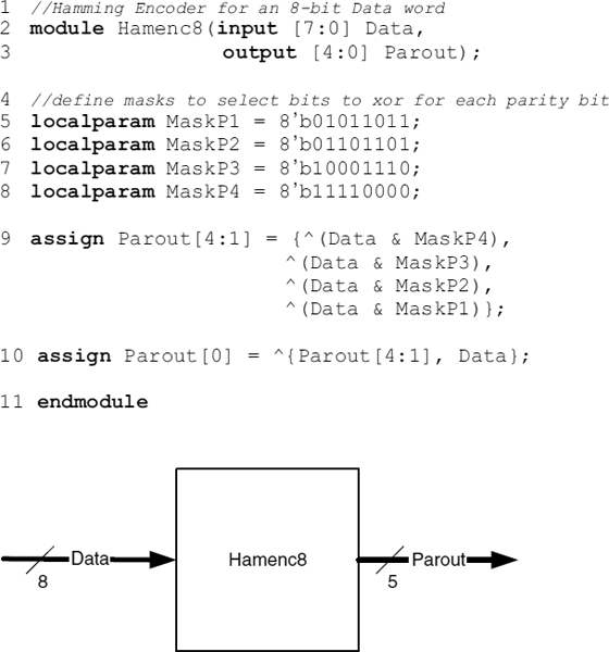
Figure 7.18 An 8-bit Hamming code encoder.
Lines 2 and 3 of Figure 7.18 define the module header for the Hamming encoder, the output Parout is a set of five parity check bits generated by performing the exclusive OR operation on subsets of the incoming 8-bit data value appearing on input port Data.
The bits of the input data that are to be exclusive ORed together are defined by a set of masks declared as local parameters on lines 5 to 8. The localparam keyword allows the definition of parameters or constant values that are local to the enclosing module, i.e. they cannot be overridden by external values. For example, mask MaskP1 defines the subset of data bits that must be processed to generate Parout[1], as shown below:
Bit position -> 76543210
    MaskP1 = 8'b01011011;
Parout[1] = Data[6]^Data[4]^Data[3]^Data[1]^Data[0];
The above modulo-2 summation is achieved in module Hamenc8 by first masking out the bits to be processed using the bitwise AND operation (&), then combining these bit values using the reduction exclusive OR operator. These operations are performed for each parity bit as part of the continuous assignment on line 9:
^(Data & MaskP1)
The concatenation operator ({ }) is used on the right-hand side of the continuous assignment on line 9 to combine the four most significant parity check bits in order to assign them to Parout[4:1].
The double-error-detecting ability of the Hamming code is provided by the overall parity check bit Parout[0]. This output is generated by modulo-2 summing (exclusive OR) all of the data bits along with the aforementioned parity bits, this being achieved on line 10 of Figure 7.18 by a combination of concatenation and reduction, as repeated below:
assign Parout[0] = ^{Parout[4:1], Data};
In performing the above operation, certain data bits are eliminated from the result due to cancellation, this is caused by the fact that the exclusive OR operation results in logic 0 when the same bit is combined an even number of times. The overall parity bit is therefore given by the following expression:
Parout[0] = Data[7]^Data[5]^Data[4]^Data[2]^Data[1]^Data[0];
Data bits Data[6] and Data[3] are not included in the above equation for the overall parity. This is reflected in the logic diagram of the Hamming encoder, shown in Figure 7.19; this circuit could represent the output produced by a logic synthesis software tool after processing the Verilog description of the Hamming encoder shown in Figure 7.18.
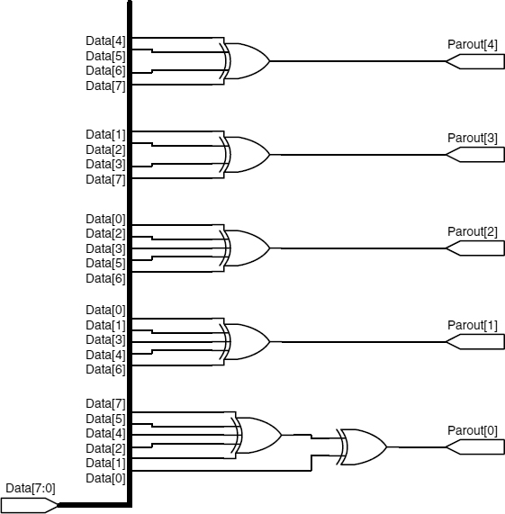
Figure 7.19 Hamming encoder logic diagram.
7.3.1 Simulating the Hamming Encoder
The operation of the Hamming encoder module shown in Figure 7.18 could be verified by simulation in an empirical manner. This would involve applying a set of random input data bytes and comparing the resulting parity check bit outputs against the values predicted from the encoder Boolean equations.
An alternative, and more systematic, approach would be to make use of a Hamming code decoder to decode the encoder output automatically, thus providing a more robust checking mechanism (assuming the Hamming decoder is correct of course!).
The use of a Hamming decoder module also allows the investigation of the error-correcting and -detecting properties of the Hamming code, by virtue of being able to introduce single and double errors into the Hamming code prior to processing by the decoder.
A Verilog HDL description of an 8-bit Hamming code decoder is given in Listing 7.3.
//Verilog description of a 13-bit Hamming Code Decoder
1 module Hamdec8(input [7:0] Datain,
     input[4:0] Parin,
     output reg[7:0] Dataout,
     output reg[4:0] Parout,
     output reg NE, DED, SEC);

  //define masks to select bits to xor for each parity
2 localparam MaskP1 = 8'b01011011;
3 localparam MaskP2 = 8'b01101101;
4 localparam MaskP4 = 8'b10001110;
5 localparam MaskP8 = 8'b11110000;

6 reg[4:1] synd; //error syndrome
7 reg P0; //regenerated overall parity

8 always @(Datain or Parin)
9 begin

      //assign default outputs (assumes no errors)
10 NE = 1'b1;
11 DED = 1'b0;
12 SEC = 1'b0;
13 Dataout = Datain;
14 Parout = Parin;
15 P0 = ^{Parin, Datain} ; //overall parity
16
   //generate syndrome bits
17 synd[4] = (^(Datain & MaskP8))^Parin[4];
18 synd[3] = (^(Datain & MaskP4))^Parin[3];
19 synd[2] = (^(Datain & MaskP2))^Parin[2];
20 synd[1] = (^(Datain & MaskP1))^Parin[1];
21 if ((synd == 0) && (P0 == 1'b0)) //no errors
22   ; //accept default o/p
23 else if (P0 == 1'b1) //single error (or odd no!)
24 begin

25   NE = 1'b0;
26   SEC = 1'b1;
   //correct single error
27 case  (synd)
28   0: Parout[0] =~Parin[0];
29   1: Parout[1] =~Parin[1];
30   2: Parout[2] =~Parin[2];
31   3: Dataout[0] =~Datain[0];
32   4: Parout[3] =~Parin[3];
33   5: Dataout[1] =~Datain[1];
34   6: Dataout[2] =~Datain[2];
35   7: Dataout[3] =~Datain[3];
36   8: Parout[4] =~Parin[4];
37   9: Dataout[4] =~Datain[4];
38   10: Dataout[5] =~Datain[5];
39   11: Dataout[6] =~Datain[6];
40   12: Dataout[7] =~Datain[7];
41 default:
42    begin
43      Dataout = 8'b00000000;
44      Parout = 5'b00000;
45    end
46  endcase
47 end
48 else if ((P0 == 0) && (synd != 4'b0000))
49 begin //double error
50   NE = 1'b0;
51   DED = 1'b1;
52   Dataout = 8'b00000000;
53   Parout = 5'b00000;
54 end
55 end //always
56
57 endmodule
Listing 7.3 An 8-bit Hamming code decoder.
The module header on line 1 of Listing 7.3 defines the interface of the decoder, the 13-bit Hamming code input is made up from Datain and Parin and the corrected outputs are on ports Dataout and Parout. Three diagnostic outputs are provided to indicate the status of the incoming code:
- NE: no errors (Datain and Parin are passed through unchanged)
- DED: double error detected (Dataout and Parout are set to all zeros)
- SEC: single error corrected (a single-bit error has been corrected1).
Note that all of the Hamming decoder outputs are qualified as being of type reg; this is due to the behavioural nature of the Verilog description, i.e. the outputs are assigned values from within a sequential always block (starting on line 8).
Lines 2 to 5 define the same set of 8-bit masks as those declared within the encoder module; they are used in a similar manner within the decoder to generate the 4-bit code named synd, declared in line 6. This 4-bit code is known as the error syndrome; it is used in combination with the regenerated overall parity bit P0 (line 7) to establish the extent and location of any errors within the incoming Hamming codeword.
The main part of the Hamming decoder is contained within the always sequential block starting on line 8 of Listing 7.3. The statements enclosed between the begin and end keywords, situated on lines 9 and 55 respectively, execute sequentially whenever there is a change in either (or both) of the Datain and Parin ports. The always block represents a behavioural description of a combinational logic system that decodes the Hamming codeword.
At the start of the sequential block, the module outputs are all assigned default values corresponding to the ‘no errors’ condition (lines 10 to 14); this ensures that the logic described by the block is combinatorial. Following this, on lines 15 to 20 inclusive, the overall parity and syndrome bits are generated using expressions similar to those employed within the encoder description.
Starting on line 21, a sequence of conditions involving the overall parity and syndrome bits is tested, in order to establish whether or not any errors are present within the incoming codeword.
If the overall parity is zero and the syndrome is all zeros, then the input codeword is free of errors and the presence of the null statement (;) on line 22 allows the default output values to persist.
If the first condition tested by the if…else statement is false, then the next condition (line 23) is tested to establish whether a single error has occurred. If the overall parity is a logic 1, then the decoder assumes that a single error has occurred; the statements between lines 24 and 47 flag this fact by first setting the ‘single error’ (SEC) output high before going on to correct the error. The latter is achieved by the use of the case statement on lines 27 to 46; the value of the 4-bit syndrome is used to locate and invert the erroneous bit.
Finally, the if…else statement tests for the condition of unchanged overall parity combined with a nonzero syndrome; this indicates a double error. Under these circumstances, the Hamming decoder cannot correct the error and, therefore, it simply asserts the ‘double error detected’ output and sets the Dataout and Parout port signals to zero.
The Hamming code encoder and decoder are combined in a Verilog test module named TestHammingCcts, shown in Listing 7.5, and in block diagram form in Figure 7.20. An additional module, named InjectError, is required to inject errors into the valid Hamming code produced by the Hamming encoder prior to being decoded by the Hamming decoder.
The InjectError module is given in Listing 7.4.
//Module to inject errors into Hamming Code
1 module InjectError(input[7:0] Din,
      input[4:0] Pin,
      output[7:0] Dout,
      output[4:0] Pout,
      input[12:0] Ein);
2 assign {Dout, Pout} = {Din, Pin} ^ Ein;

3 endmodule
Listing 7.4 The 13-bit error injector module.
This uses a single continuous assignment to invert selectively one or more of the 13 bits of the incoming Hamming codeword by exclusive ORing it with a 13-bit error mask named Ein, in line 2.
As shown in the block diagram of Figure 7.20 and Listing 7.5, the test module comprises instantiations of the encoder, decoder and error injector (lines 33 to 46) in addition to two initial sequential blocks named gen_data and gen_error, these being situated on lines 13 and 20 respectively of Listing 7.5.
// Verilog test fixture for Hamming Encoder and Decoder
1 ‘timescale 1ns / 1ns
2 module TestHammingCcts();

  //Hamming encoder data input
3   reg[7:0] Data;
  //Error mask pattern
4   reg[12:0] Error;
  //Hamming encoder output
5   wire[4:0] Par;
  //Hamming code with error
6   wire[7:0] EData;
7   wire[4:0] EPar;
//Hamming decoder outputs
8   wire DED;
9   wire NE;
10 wire SEC;
11 wire[7:0] Dataout;
12 wire[4:0] Parout;

13 initial //generate exhaustive test data
14 begin : gen_data
15    Data = 0;
16    repeat (256)
17      #100 Data = Data + 1;
18    $stop;
19 end

20 initial //generate error patterns
21 begin : gen_error
22   Error = 13'b0000000000000;
23   #1600;
24   Error = 13'b0000000000001;
25     #100;
26   repeat (100) //rotate single error
27     #100 Error = {Error[11:0], Error[12]};
28   Error = 13′b0000000000011;
29     #100;
30   repeat (100) //rotate double error
31     #100 Error = {Error[11:0], Error[12]};
32 end

//instantiate modules

33 Hamenc8 U1 (.Data(Data),
34            .Parout(Par));
35 Hamdec8 U2 (.Datain(EData),
36            .Parin (EPar),
37            .Dataout(Dataout),
38            .DED(DED),
39            .NE(NE),
40            .Parout(Parout),
41            .SEC(SEC));
42 InjectError U3 (.Din(Data),
43            .Ein(Error),
44            .Pin(Par),
45            .Dout(EData),
46            .Pout(EPar));
47 endmodule
Listing 7.5 Hamming encoder/decoder test-fixture module.
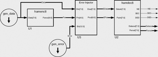
Figure 7.20 Hamming encoder/decoder test-fixture block diagram.
The gen_data initial block uses the repeat loop to generate an exhaustive set of 8-bit input data values ascending from 010 to 25510 at intervals of 100 ns, stopping the simulation on line 18 by means of the $stop command. The gen_error block, on lines 20 to 32, starts by initializing the error mask Error to all zeros and allows it to remain in this state for 1600 ns in order to verify the ‘no error’ condition.
On line 24 of Listing 7.5, the error mask is set to 13'b0000000000001, thereby introducing a single-bit error into the least significant bit of the Hamming codeword. After applying this pattern for 100 ns, a repeat loop (lines 26 and 27) is used to rotate the single-bit error through all 13 bits of the error mask at intervals of 100 ns for 100 iterations, this sequence will demonstrate the Hamming decoder's ability to correct a single-bit error in any bit position for a variety of test data values.

Figure 7.21 TestHammingCcts simulation results showing: (a) no errors; (b) single-error correction; (c) double-error detection.
Finally, on lines 28 to 31, the error mask is reinitialized to a value of 13'b0000000000011. This has the effect of introducing a double-error into the Hamming codeword. As above, this pattern is rotated through all 13-bits of the Hamming code 100 times, at intervals of 100 ns, in order to verify the decoder's ability to detect double errors for a variety of test data. Simulation results for the TestHammingCcts test module are shown in Figure 7.21a–c.
Figure 7.21a shows the first 16 test pattern results corresponding to an error mask value of all zeros (third waveform from the top), i.e. no errors. The top two waveforms are the 8-bit data (Data) and 5-bit parity (Par) values representing the 13-bit Hamming code output of the Hamming encoder module; all waveforms are displayed in hexadecimal format.
The outputs of the error injector module (EData and EPar), shown on the fourth and fifth waveforms, are identical to the top two waveforms due to the absence of errors. The diagnostic outputs, SEC, NE and DED, correctly show the ‘no errors’ output asserted, while the bottom two waveforms show the Hamming code being passed through the decoder unchanged.
Figure 7.21b shows a selection of test pattern results corresponding to an error mask containing a single logic 1 (third waveform from the top), i.e. a single error.
The outputs of the error injector module (EData and EPar), shown on the fourth and fifth waveforms, differ when compared with the top two waveforms by a single bit (e.g. 2A16, 1016 becomes AA16, 1016 at time 4.2 μs). The diagnostic outputs, SEC, NE and DED, correctly show the ‘single error corrected’ output asserted, while the bottom two waveforms confirm that the single error introduced into the original Hamming code (top two waveforms) has been corrected after passing through the decoder.
Figure 7.21c shows a selection of test pattern results corresponding to an error mask containing two logic 1s (third waveform from the top), i.e. a double error.
The outputs of the error injector module (EData and EPar), shown on the fourth and fifth waveforms, differ when compared with the top two waveforms by 2 bits (e.g. BC16, 1C16 becomes BA16, 1C16 at time 18.8 μs). The diagnostic outputs, SEC, NE and DED, correctly show the ‘double error detected’ output asserted, while the bottom two waveforms confirm that the double error introduced into the original Hamming code (top two waveforms) has been detected and the output codeword is set to all zeros.
In summary, this section has presented a realistic example of the use of the Verilog HDL operators and types to describe a Hamming code encoder, decoder and test module. The behavioural style of description has been used to illustrate the power of the Verilog language in describing a relatively complex combinatorial logic system in a high-level manner.
Chapter 8 covers those aspects of the Verilog language concerned with the description of sequential logic systems, in particular the FSM.
REFERENCES
1. Ciletti M.D. Modeling, Synthesis and Rapid Prototyping with the Verilog HDL. New Jersey: Prentice Hall, 1999.
2. Wakerly J.F. Digital Design: Principles and Practices, 4th Edition. New Jersey: Pearson Education, 2006 (Hamming codes: p. 61, section 2.15.3).
1 An odd number of erroneous bits greater than one would be handled as a single error, usually resulting in an incorrect output.).