
8
Describing Combinational and Sequential Logic using Verilog HDL
8.1 THE DATA-FLOW STYLE OF DESCRIPTION: REVIEW OF THE CONTINUOUS ASSIGNMENT
We have already come across numerous examples in the previous chapters of Verilog designs written in the so-called data-flow style. This style of description makes use of the parallel statement known as a continuous assignment. Predominantly used to describe combinational logic, the flow of execution of continuous assignment statements is dictated by events on signals (usually wires) appearing within the expressions on the left- and right-hand sides of the continuous assignments. Such statements are identified by the keyword assign. The keyword is followed by one or more assignments terminated by a semicolon.
All of the following examples describe combinational logic, this being the most common use of the continuous assignment statement:
//some continuous assignment statements
   assign A = q [0], B = q [1], C = q [2];

   assign out = (~s1 & ~s0 & i0) |
       (~s1 & s0 & i1) |
       (s1 & ~s0 & i2) |
       (s1 & s0 & i3);

  assign #15 {c_out, sum} = a + b + c_in;
The continuous assignment statement forms a static binding between the wire being assigned on the left-hand side of the = operator and the expression on the right-hand side of the assignment operator. This means that the assignment is continuously active and ready to respond to any changes to variables appearing in the right-hand side expression (the inputs). Such changes result in the evaluation of the expression and updating of the target wire (output). In this manner, a continuous assignment is almost exclusively used to describe combinatorial logic.

Figure 8.1 Describing a level-sensitive latch using a continuous assignment.
As mentioned previously, a Verilog module may contain any number of continuous assignment statements; they can be inserted anywhere between the module header and internal wire/reg declarations and the endmodule keyword.
The expression appearing on the right-hand side of the assignment operator may contain both reg- and wire-type variables and make use of any of the Verilog operators mentioned in Chapter 7.
The so-called target of the assignment (left-hand side) must be a wire, since it is continuously driven. Both single-bit and multi-bit wires may be the targets of continuous assignment statements.
It is possible, although not common practice, to use the continuous assignment statement to describe sequential logic, in the form of a level-sensitive latch.
The conditional operator (?:) is used on the right-hand side of the assignment on line 2 of the listing shown in Figure 8.1. When en is true (logic 1) the output q is assigned the value of the input data continuously. When en goes to logic 0, the output q is assigned itself, i.e. feedback maintains the value of q, as shown in the logic diagram below the Verilog listing.
It should be noted that the use of a continuous assignment to create a level-sensitive latch, as shown in Figure 8.1, is relatively uncommon. Most logic synthesis software tools will issue a warning message on encountering such a construct.
8.2 THE BEHAVIOURAL STYLE OF DESCRIPTION: THE SEQUENTIAL BLOCK
The Verilog HDL sequential block defines a region within the hardware description containing sequential statements; these statements execute in the order they are written, in just the same way as a conventional programming language. In this manner, the sequential block provides a mechanism for creating hardware descriptions that are behavioural or algorithmic. Such a style lends itself ideally to the description of synchronous sequential logic, such as counters and FSMs; however, sequential blocks can also be used to describe combinational functions.
A discussion of some of the more commonly used Verilog sequential statements will reveal their similarity to the statements used in the C language. In addition to the two types of sequential block described below, Verilog HDL makes use of sequential execution in the so-called task and function elements of the language. These elements are beyond the scope of this book; the interested reader is referred to Reference [1].
Verilog HDL provides the following two types of sequential block:
- The always block. This contains sequential statements that execute repetitively, usually in response to some sort of trigger mechanism. An always block acts rather like a continuous loop that never terminates. This type of block can be used to describe any type of digital hardware.
- The initial block. This contains sequential statements that execute from beginning to end once only, commencing at the start of a simulation run at time zero. Verilog initial blocks are used almost exclusively in simulation test fixtures, usually to create test input stimuli and control the duration of a simulation run. This type of block is not generally used to describe synthesizable digital hardware, although a simulation model may contain an initial statement to perform an initialization of memory or to load delay data.
The two types of sequential block described above are, in fact, parallel statements; therefore, a module can contain any number of them. The order in which the always and initial blocks appear within the module does not affect the way in which they execute. In this sense, a sequential block is similar to a continuous assignment: the latter uses a single expression to assign a value to a target whenever a signal on the right-hand side undergoes a change, whereas the former executes a sequence of statements in response to some sort of triggering event.
Figure 8.2 shows the syntax of the initial sequential block, along with an example showing how the construct can be used to generate a clock signal.
As can be seen in lines 3 to 8, an initial block contains a sequence of one or more statements enclosed within a begin…end block. Occasionally, there is only a single statement enclosed within the initial block; in this case, it is permissible to omit the begin…end bracketing, as shown in lines 12 and 13. It is recommended, however, that the bracketing is included, regardless of the number of sequential statements, in order to minimize the possibility of syntax errors.
Figure 8.2 also includes an example initial block (lines 14 to 21), the purpose of which is to generate a repetitive clock signal. A local parameter named PERIOD is defined in line 14; this sets the time period of the clock waveform to 100 time-units. The execution of the initial block starts at time zero at line 18, where the CLK signal is initialized to logic 0; note that the signal CLK must be declared as a reg, since it must be capable of retaining the value last assigned to it by statements within the sequential block. Also note that the initialization of CLK could have been included as part of its declaration in line 15, as shown below:
15 reg CLK = 1'b0;

Figure 8.2 Syntax of the initial block and an example.
Following initialization of CLK to logic 0, the next statements to execute within the initial block are lines 19 and 20 of the listing in Figure 8.2. These contain an endless loop statement known as a forever loop, having the general syntax shown below:
In common with the initial block itself, the forever loop may contain a single statement or a number of statements that are required to repeat indefinitely; in the latter case, it must include the begin…end bracketing shown above. The example shown in Figure 8.2 contains a single delayed sequential assignment statement in line 20 (the use of the hash symbol # within a sequential block indicates a time delay). The effect of this statement is to invert the CLK signal every 50 time-units repetitively; this results in the CLK signal having the waveform shown at the bottom of Figure 8.2.
As it stands, the Verilog description contained in lines 14–21 of Figure 8.2 could present a potential problem to a simulator, in that most such tools have a command to allow the simulator to effectively run forever (e.g. ‘run –all’ in Modelsim®). The forever loop in lines 19 and 20 would cause a simulator to run indefinitely, or at least until the host computer ran out of memory to store the huge amount of simulation data generated.
There are two methods by which the above problem can be solved:
- Include an additional initial block containing a $stop system command.
- Replace the forever loop with a repeat loop.
The first solution involves adding the following statement:
//n is the no. of clock pulses required
initial #(PERIOD*n) $stop;
The above statement can be inserted anywhere after line 14 within the module containing the statements shown in Figure 8.2. The execution of the initial block in line 16 commences at the same time as the statement shown above (0 s); therefore, the delayed $stop command will execute at an absolute time equal to n*PERIOD seconds. The result is a simulation run lasting exactly n clock periods. It should be noted that, in order for the above statement to compile correctly, the variable n would have to be replaced by an actual positive number or would have to have been previously declared as a local parameter.
The second solution involves modifying the initial block in lines 16–21 of the listing given in Figure 8.2 to that shown below:
1  initial
2  begin
3     CLK = 1'b0;
4     repeat (n) //an finite loop
5  begin
6     #(PERIOD/2) CLK = 1'b1;
7     #(PERIOD/2) CLK = 1'b0;
8  end
9  $stop;
10 end
The repeat loop is a sequential statement that causes one or more statements to be repeated a fixed number of times. In the above case, the variable n defines the number of whole clock periods required during the simulation run. In this example, the loop body contains two delayed assignments to the reg named CLK; consequently, the begin…end bracketing is required.
Each repetition of the repeat loop lasts for 100 time-units, i.e. one clock period. Once all of the clock pulses have been applied, the repeat loop terminates and the simulation is stopped by the system command in line 9 above.
An important point to note regarding the repeat and forever loops is that neither can be synthesized into a hardware circuit; consequently, these statements are exclusively used in Verilog test-fixtures or within simulation models.
Listing 8.1a–e shows the various formats of the Verilog HDL sequential block known as the always block. The most general form is shown in Listing 8.1a: the keyword always is followed by the so-called event expression; this determines when the sequential statements in the block (between begin and end) execute. The @(event expression) is required for both combinational and sequential logic descriptions.
In common with the initial block, the begin…end block delimiters can be omitted if there is only one sequential statement subject to the always @ condition. An example of this is shown in Listing 8.1e.
(a)
  1  always @(event_expression)
  2  begin
  3    //sequential statement 1
  4    //sequential statement 2
  5    …
  6  end

(b)
  1  always @ (input1 or input2 or input3…)
  2  begin
  3   //sequential statement 1
  4   //sequential statement 2
  5   …
  6  end

(c)
  1  always @(input1, input2, input3…)
  2  begin
  3   //sequential statement 1
  4   //sequential statement 2
  5   …
  6  end

(d)
  1  always @( * )
  2  begin
  3        //sequential statement 1
  4        //sequential statement 2
  5   …
  6  end

(e)
  1  always @(a)
  2        y = a * a;
Listing 8.1 Alternative formats for the always sequential block: (a) General form of the always sequential block; (b) always sequential block with or-separated list; (c) always sequential block with comma-separated list; (d) always sequential block with wildcard event expression; (e) always sequential block containing a single sequential statement.
Unlike the initial block, the sequential statements enclosed within an always block execute repetitively, in response to the event expression. After each execution of the sequential statements, the always block usually suspends at the beginning of the block of statements, ready to execute the first statement in the sequence. When the event expression next becomes true, the sequential statements are then executed again. The exact nature of the event expression determines the nature of the logic being described; as a general guideline, any of the forms shown in Listing 8.1 can be used to describe combinational logic. However, the format shown in Listing 8.1b is most commonly used to describe sequential logic, with some modification (see later).
Also in common with the initial block, signals that are assigned from within an always block must be reg-type objects, since they must be capable of retaining the last value assigned to them during suspension of execution.
It should be noted that the always block could be used in place of an initial block, where the latter contains a forever loop statement. For example, the following always block could be used within a test module to generate the clock waveform shown in Figure 8.2:
1  localparam PERIOD = 100; //clock period

  2  reg CLK = 1'b0;

  3  always
  4  begin
  5     #(PERIOD/2) CLK = 1'b1;
  6     #(PERIOD/2) CLK = 1'b0;
  7  end
The always sequential block, shown in lines 3 to 7 above, does not require an event expression since the body of the block contains sequential statements that cause execution to be suspended for a fixed period of time.
This example highlights an important aspect of the always sequential block: it must contain either at least one sequential statement that causes suspension of execution or the keyword always must be followed by an event expression (the presence of both is ambiguous and, therefore, is not allowed).
The absence of any mechanism to suspend execution in an always block will cause a simulation tool to issue an error message to the effect that the description contains a zero-delay infinite loop, and the result is that the simulator will ‘hang’, being unable to proceed beyond time zero.
In summary, the use of an always block in a test module, as shown above, is not recommended owing to the need to distinguish clearly between modules that are intended for synthesis and implementation and those that are used during simulation only.
8.3 ASSIGNMENTS WITHIN SEQUENTIAL BLOCKS: BLOCKING AND NONBLOCKING
An always sequential block will execute whenever a signal change results in the event expression becoming true. In between executions, the block is in a state of suspension; therefore, any signal objects being assigned to within the block must be capable of remembering the value that was last assigned to them. In other words, signal objects that are assigned values within sequential blocks are not continuously driven. This leads to the previously stated fact that only reg-type objects are allowed on the left-hand side of a sequential assignment statement.
The above restriction regarding objects that can be assigned a value from within a sequential block does not apply to those that appear in the event expression, however. A sequential block can be triggered into action by changes in both regs and/or wires; this means that module input ports, as well as gate outputs and continuous assignments, can cause the execution of a sequential block and, therefore, behavioural and data-flow elements can be mixed freely within a hardware description.
8.3.1 Sequential Statements
Table 8.1 contains a list of the most commonly used sequential statements that may appear within the confines of a sequential block (initial or always); some are very similar to those used in the C language, while others are unique to the Verilog HDL.
A detailed description of the semantics of each sequential statement is not included in this section; instead, each statement will be explained in the context of the examples that follow. It should also be noted that Table 8.1 is not exhaustive; there are several less commonly used constructs, such as parallel blocks (fork…join) and procedural continuous assignments, that the interested reader can explore further in Reference [1].
With reference to Table 8.1, items enclosed within square brackets ( [ ] ) are optional, curly braces ( { } ) enclose repeatable items, and all bold keywords must be lower case.
Table 8.1 The most commonly used Verilog HDL sequential statements.
| Sequential statement | Description |
| = | Blocking sequential assignment |
| <= | Nonblocking sequential assignment |
| ; | Null statement. Also required at the end of each statement |
begin {seq_statements} end |
Block or compound statement. Always required if there is more than one sequential statement |
if(expr) seq_statement [else seq_statement ] |
Conditional statement, expression (expr) must be in parentheses. The else part is optional and the statement may be nested. Multiple statements require begin…end bracketing |
case(expr) { {value,} : seq_statement} [default: seq_statement] endcase |
Multi-way decision, the expression (expr) must be in parentheses. Multiple values are allowed in each limb, but no overlapping values are allowed between limbs. Default limb is required if previous values do not cover all possible values of expression. Multiple statements require begin…end bracketing |
forever
  seq_statement
|
Unconditional loop. Multiple statements require begin…end bracketing |
repeat (expr)
  seq_statement
|
Fixed repetition of seq_statement a number of times equal to expr. Multiple statements require begin…end bracketing |
while (expr)
  seq_statement
|
Entry test loop (same as C) repeats as long as expr is nonzero. Multiple statements require begin…end bracketing |
for (exp1;exp2;exp3)
  seq_statement
|
Universal loop construct (same as C). Multiple statements require begin…end bracketing |
#(time_value) seq_statement |
Suspends a block for time_value time-units |
@(event_expr) seq_statement |
Suspends a block until event_expr triggers |
The continuous assignment parallel statement makes use of the = assignment operator exclusively. As shown in Table 8.1, sequential assignments can make use of two different types of assignment:
- blocking assignment – uses the = operator;
- nonblocking assignment – uses the <= operator.
The difference between the above assignments is quite subtle and can result in simulation and/or synthesis problems if not fully understood.
The blocking assignment is the most commonly used type of sequential assignment when describing combinational logic. As the name suggests, the target of the assignment is updated before the next sequential statement in the sequential block is executed, in much the same way as in a conventional programming language. In other words, a blocking assignment ‘blocks’ the execution of the subsequent statements until it has completed. Another aspect of blocking sequential assignments is that they effectively overwrite each other when assignments are made to the same signal. An example of this is seen in the Hamming code decoder example at the end of Chapter 7 (see Listing 7.3), where the decoder outputs are initialized to a set of default values prior to being conditionally updated by subsequent statements.
On encountering a nonblocking assignment, the simulator schedules the assignment to take place at the beginning of the next simulation cycle, this normally occurs at the end of the sequential block (or at the point when the sequential block is next suspended). In this manner, subsequent statements are not blocked by the assignment, and all assignments are scheduled to take place at the same point in time.
Nonblocking assignments can be used to assign several reg-type objects synchronously, under control of a common clock. This is illustrated by the example shown in Figure 8.3.
The three nonblocking assignments on lines 17, 18 and 19 of the listing shown in Figure 8.3 are all scheduled to occur at the positive edge of the signal named ‘CLK’. This is achieved by means of the event expression on line 15 making use the event qualifier posedge (derived from positive-edge), i.e. the execution of the always sequential block is triggered by the logic 0 to logic 1 transition of the signal named CLK. This particular form of triggering is commonly used to describe synchronous sequential logic and will be discussed in detail later in this chapter.
The nonblocking nature of the assignments enclosed within the sequential block means that the value being assigned to R2 at the first positive edge of the clock, for example, is the current value of R1, i.e. ‘unknown’ (1'bx). The same is true for the value being assigned to R3 at the second positive edge of CLK; that is, the current value of R2, which is also 1'bx. Hence, the initial unknown states of R1, R2 and R3 are successively changed to logic 0 after three clock pulses; in this manner, the nonblocking assignments describe what is, in effect, a 3-bit shift register, as shown in Figure 8.4.
Figure 8.5 shows an almost identical listing to Figure 8.3, apart from the three assignments in lines 17, 18 and 19, which in this case are of the blocking variety. The initial value of regs R1, R2 and R3 is unknown as before, and the reg R0 is initialized at time zero to logic 0.
The effect of the blocking assignments is apparent in the resulting simulation result shown in Figure 8.5: all three signals change to logic 0 at the first positive edge of the CLK. This is due to the fact that the blocking assignment updates the signal being assigned prior to the next statement in the sequential block. The result is that the three assignments become what is, in effect, one assignment of the value of R0 to R3. The equivalent circuit of the always block listed in Figure 8.5 is shown in Figure 8.6.
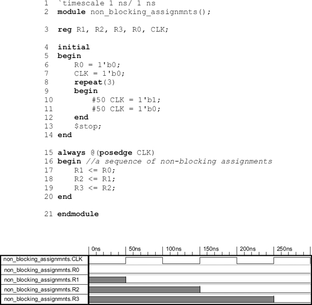
Figure 8.3 Illustration of nonblocking assignments.
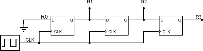
Figure 8.4 Nonblocking assignment equivalent circuit.

Figure 8.5 Illustration of blocking assignments.
The choice of whether to use blocking or nonblocking assignments within a sequential block depends on the nature of the digital logic being described. Generally, it is recommended that nonblocking assignments are used when describing synchronous sequential logic, whereas blocking assignments are used for combinational logic.

Figure 8.6 Blocking assignment equivalent circuit.
Sequential blocks intended for use within test modules are usually of the initial type; therefore, blocking assignments are the most appropriate choice.
A related point regarding the above guidelines is that blocking and nonblocking assignments should not be mixed within a sequential block.
8.4 DESCRIBING COMBINATIONAL LOGIC USING A SEQUENTIAL BLOCK
The rich variety of sequential statements that can be included within a sequential block means that the construct can be used to describe virtually any type of digital logic. Figure 8.7 shows the Verilog HDL description of a multiplexer making use of an always sequential block.
The module header in line 1 declares the output port out as a reg, since it appears on the left-hand side of an assignment within the sequential block. This example illustrates that despite the keyword reg being short for register, it is often necessary to make use of the reg object when describing purely combinational logic.
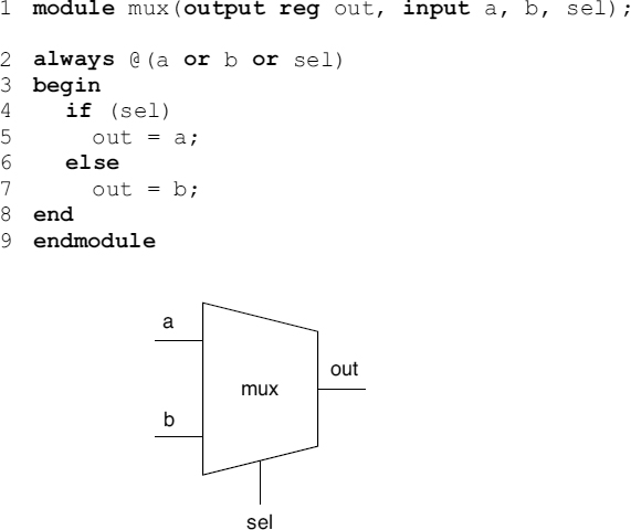
Figure 8.7 A two-input multiplexer described using an always block.
The event expression in line 2 of the listing in Figure 8.7 includes all of the inputs to the block in parentheses and separated by the keyword or. This format follows the original Verilog-1995 style; the more recent versions of the language allow either a comma-separated list or the use of the wildcard ‘*’ to mean any reg or wire referenced on the right-hand side of an assignment within the sequential block.
Regardless of the event expression format used, the meaning is the same, in that any input change will trigger execution of the statements within the block.
The sequential assignments in lines 5 and 7 are of the nonblocking variety, as recommended previously. The value assigned to out is either the a input or the b input, depending on the state of the select input sel.
One particular aspect of using an always sequential block to describe combinational logic is the possibility of creating an incomplete assignment. This occurs when, for example, an if…else statement omits a final else part, resulting in the reg target signal retaining the value that was last assigned to it.
In terms of hardware synthesis, such an incomplete assignment will result in a latch being created. Occasionally, this may have been the exact intention of the designer; however, it is a more common situation that the designer has inadvertently omitted a final else or forgotten to assign a default value to the output. In either case, most logic synthesis software tools will issue warning messages if they encounter such a situation.
The following guidelines should be observed when describing purely combinational logic using an always sequential block:
Include all of the inputs to the combinatorial function in the event expression using one of the formats shown in Listing 8.1b–d.
To avoid the creation of unwanted latches, ensure either of the following is applicable:
- assign a default value to all outputs at the top of the always block, prior to any sequential statement such as if, case, etc.;
- in the absence of default assignments, ensure that all possible combinations of input conditions result in a value being assigned to the outputs.
The example in Figure 8.8 illustrates the points discussed above regarding incomplete assignments.
The designer of the module latch_implied listed in Figure 8.8 has used an always block to describe the behaviour of a selector circuit. The 2-bit input sel [1:0] selects one of three inputs a, b or c and feeds it through to the output y.
The assumption has been made that y will be driven to logic 0 if sel is equal to 2'b11. This is, of course, incorrect: the omission of a final else clause results in y retaining its current value (since it is a reg), hence the presence of the feedback connection between the y output and the lower input of the left-hand multiplexer of the circuit shown in Figure 8.8. The synthesis tool has correctly inferred a latch from the semantics of the if…else statement and the reg object.
There are two alternative ways in which the listing in Figure 8.8 may be modified in order to remove the presence of the inferred latch in the synthesized circuit. These are shown in Figure 8.9a and b, with the corresponding latch-free circuit shown in Figure 8.9c.
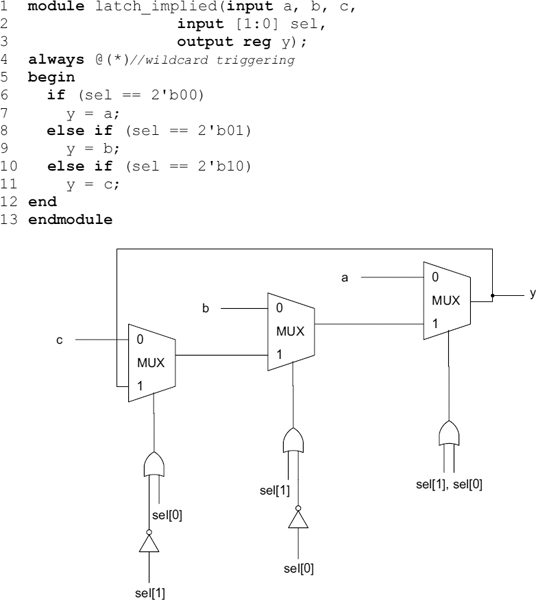
Figure 8.8 Example showing latch inference.
The listing shown in Figure 8.9a adds a final else part in lines 12 and 13; this has the effect of always guaranteeing the output y is assigned a value under all input conditions. Figure 8.9b achieves the same result by assigning a default value of logic 0 to output y in line 6.
Of the alternative strategies for latch removal exemplified above, the use of default assignments at the beginning of the sequential block is the more straightforward of the two to apply; therefore, this is the recommended approach to eliminating this particular problem.
The following examples further illustrate how the Verilog HDL can be used to describe a combinational logic function using an always sequential block. The first example, shown in Figure 8.10, describes a three-input to eight-output decoder (similar to the TTL device known as the 74LS138).
The function of the ttl138 module is to decode a 3-bit input ![]() A, B, C
A, B, C![]() , and assert one of eight active-low outputs. The decoding is enabled by the three G inputs
, and assert one of eight active-low outputs. The decoding is enabled by the three G inputs ![]() G1, G2A, G2B
G1, G2A, G2B![]() , which must be set to the value
, which must be set to the value ![]() 1,0,0
1,0,0![]() . If the enable inputs are not equal to
. If the enable inputs are not equal to ![]() 1,0,0
1,0,0![]() , then all of the Y outputs are set high.
, then all of the Y outputs are set high.
This behaviour is described using an always sequential block that responds to changes on all inputs, starting in line 3 of the listing shown in Figure 8.10. The Y outputs are set to a default value of all ones in line 5 and this is followed by an if statement that conditionally asserts one of the

Figure 8.9 Removal of unwanted latching feedback: (a) removal of latch using final else part; (b) removal of latch using assignment of default output value; (c) synthesized circuit for (a) and (b).

Y outputs to logic 0, depending on the decimal equivalent (0–7) of ![]() A, B, C
A, B, C![]() , in lines 6 and 7 respectively.
, in lines 6 and 7 respectively.
Simulation of the ttl138 module is achieved using the Verilog test-fixture shown in Figure 8.11. The test-fixture module shown in Figure 8.11 makes use of a so-called named sequential block starting in line 6. The name of the block, gen_tests, is an optional label that must be placed after a colon following the keyword begin. Naming a sequential block in this manner (both always and initial blocks may be named) allows items, such as regs and integers, to be declared and made use of within the confines of the block. These locally declared objects may only be referenced from outside the block in which they are declared by preceding the object name with the block name; for example, the integer t in the listing of Figure 8.11 could be referenced outside of the initial block as follows:
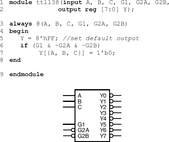
Figure 8.10 Three-to-eight decoder Verilog description and symbol.
gen_tests.t
The use of locally declared objects, as described above, allows the creation of a more structured description. However, it should be noted that, at the time of writing, not all logic synthesis tools recognize this aspect of the Verilog language.
The integer t is used within the initial block to control the iteration of the for loop situated between lines 9 and 12 inclusive. The purpose of the loop is to apply an exhaustive set of input states to the ![]() A, B, C
A, B, C![]() inputs of the decoder. The syntax and semantics of the Verilog for loop is very similar to that of its C-language equivalent, as shown below:
inputs of the decoder. The syntax and semantics of the Verilog for loop is very similar to that of its C-language equivalent, as shown below:
for (initialization; condition; increment) begin
     sequential statements
end
The above is equivalent to the following:
initialization;
while (condition) begin
sequential statements
…
increment;
end
In line 10 it can be seen how Verilog allows the 32-bit integer to be assigned directly to 3-bit concatenation of the input signals without the need for conversion.
The timing simulation results are also included in Figure 8.11; these clearly show the decoding of the 3-bit input into a one-out-of-eight output during the first 800 ns. During the last 200 ns of the simulation, the enable inputs are set to 3'b000 and then 3'b011 in order to show all of the Y outputs going to logic 1 as a result of the decoder being disabled.
Finally, it should be noted that the very simple description of the decoder given in Figure 8.10 is not intended to be an accurate model of the actual TTL device; rather, it is a simple behavioural model intended for fast simulation and synthesis.
A second example is shown in Figure 8.12. This shows the Verilog source description and symbolic representation of a majority voter capable of accepting an n-bit input word. The function of this module is to drive a single-bit output named maj to either a logic 1 or logic 0 corresponding to the majority value of the input bits. Clearly, such a module requires an odd number of input bits greater than or equal to 3 in order to produce a meaningful output.
The module header (lines 2 and 3 of the listing in Figure 8.12) includes a parameter named n to set the number of input bits, having a default value of 5. The use of a parameter makes the majority voter module potentially more useful due to it being scalable, i.e. the user simply sets the parameter to the desired value as part of the module instantiation.
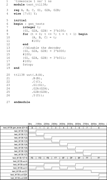
Figure 8.11 Test fixture and simulation results for the three-to-eight decoder module.

Figure 8.12 Verilog description and symbol for an n-bit majority voter.
Two register-type objects, in the form of integers are declared in line 4. The first, num_ones, is used to keep track of the number of logic 1s contained in the input A, and the second, named bit, is used as a loop counter within the for loop situated in lines 10–15. A single-bit reg named is_x is declared in line 5 to act as a flag to record the presence of any unknown or high-impedance input bits.
The behaviour of the majority voter is described using an always sequential block commencing in line 6 of the listing show in Figure 8.12. The block is triggered by changes in the input word A, and starts by initializing is_x and num_ones to their default values of zero. The for loop then scans through each bit of the input word, first checking for the presence of an unknown or high-impedance state and then incrementing num_ones each time a logic 1 is detected. Note the use of the case-equality operator (===) in line 11 to compare each input bit of A explicitly with the meta-logical values 1'bx and 1'bz:
(A [bit] === 1'bx)||(A [bit] === 1'bz)
On completion of the for loop in line 15, the sequential block suspends until subsequent events on the input A.
The output maj is continuously assigned a value based on the outcome of the always block. The expression in lines 17 and 18 assigns 1'bx to the output subject to the conditional expression being true, thereby indicating the presence of an unknown or high impedance among the input bits. In the absence of any unknown input bits, the output is determined by comparing the number of logic 1s within A (num_ones) with the total number of bits in A (n):
(n - num_ones) < num_ones
It is left to the reader to verify that the above expression is true (false), i.e. yields a logic 1 (logic 0) if num_ones is greater (less) than the number of logic 0s in the n-bit input A.
The simulation of a 7-bit majority voter module is carried out using the test module shown in Figure 8.13. This test module instantiates a 7-bit (n = 7) majority voter in line 5. The initial block starting in line 6 sets the input to all zeros in line 8 and then applies an exhaustive set of input values by means of a repeat loop in lines 9–12 inclusive. The expression 1 << 7, used to set the number of times to execute the repeat loop, effectively raises the number 2 to the power 7, by shifting a single logic 1 to the left seven times. This represents an alternative to using the ‘raise-to-the-power’ operator ‘** ’, which is not supported by all simulation and synthesis tools.
After applying all known values to the A input of the majority voter module, the test module then applies two values containing the meta-logical states (lines 14–17) in order to verify that the module correctly detects an unknown input.
Figure 8.13 also shows a sample of the simulation results produced by running the test module. Inspection of the results reveals that the module correctly outputs a logic 1 when four or more, i.e. the majority of the inputs, are at logic 1. The behaviour of the internal objects num_ones and is_x can also be seen to be correct.
8.5 DESCRIBING SEQUENTIAL LOGIC USING A SEQUENTIAL BLOCK
With the exception of the simple level-sensitive latch given in Figure 8.1, Verilog HDL descriptions of sequential logic are exclusively constructed using the always sequential block. The reserved words posedge (positive edge) and negedge (negative edge) are used within the event expression to define the sensitivity of the sequential block to changes in the clocking signal. Figure 8.14 shows the general forms of the always block that are applicable to purely synchronous sequential logic, i.e. logic systems where all signal changes occur either on the rising (a) or falling (b) edges of the global clock signal.
The use of both posedge and negedge triggering is permitted within the same event expression at the beginning of an always block; however, this does not usually imply dual-edge clocking. The use of both of the aforementioned event qualifiers is used to describe synchronous sequential logic that includes an asynchronous initialization mechanism, as will be seen later in this section.
Figure 8.15 shows the symbol and Verilog description of what is perhaps the simplest of all synchronous sequential logic devices: the positive-edge-triggered D-type flip flop.
The module header, in line 1 of the listing in Figure 8.15, declares the output Q to be a reg-type signal, owing to the fact that it must retain a value in between active clock edges. The use of the keyword reg is not only compulsory, but also highly appropriate in this case, since Q represents the state of a single-bit register.
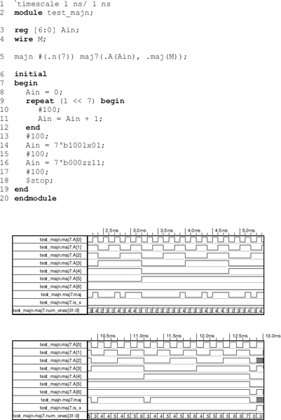
Figure 8.13 Test fixture and simulation results for the n-bit majority voter.
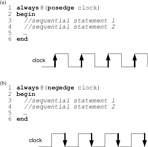
Figure 8.14 General forms of the always block when describing synchronous sequential logic: (a) positive-edge-triggered sequential logic; (b) negative-edge-triggered sequential logic.
The always sequential block in lines 2 and 3 contains a single sequential statement (hence the absence of the begin…end bracketing) that performs a nonblocking assignment of the input value D to the stored output Q on each and every positive edge of the input named CLK. In this manner, the listing given in Figure 8.15 describes an ideal functional model of a flip flop: unlike areal device, it does not exhibit propagation delays, nor are there any data set-up and hold times that must be observed. To include such detailed timing aspects would result in a far more complicated model, and this is not required for the purposes of logic synthesis.
As mentioned previously, it is conventional to use the nonblocking assignment operator when describing sequential logic. However, it is worth noting that the above flip-flop description would perform identically if the assignment in line 3 was of the blocking variety. This is due to the fact that there is only one signal being assigned a value from within the always block.

Figure 8.15 A positive-edge-triggered D-type flip-flop.
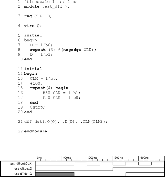
Figure 8.16 D-type flip-flop test module and waveforms.
Figure 8.16 shows a Verilog test-module and corresponding simulation waveform results for the D-type flip flop. This test module makes use of two initial sequential blocks to produce the D and CLK inputs of the flip flop. Line 8 illustrates the use of the @(event_expression) statement within a test module; in this case, the repeat loop waits for three consecutive negative-edge transitions to occur on the CLK before setting the data input D to a logic 1.
Inspection of the timing waveforms below the listing in Figure 8.16 shows that the Q output of the flip flop remains in an unknown state (shaded) until the first 0-to-1 transition of the clock; in other words, the flip-flop is initialized synchronously. In addition, the change in the data input D appears to occur at the second falling-edge of the clock, despite the fact that the repeat loop specifies three iterations; this apparent discrepancy is due to the change from the initial state of CLK, i.e. 1'bx, to 1'b0 at time zero, being equivalent to a negative edge at the very start of the simulation run. Finally, it can be seen that the Q output of the flip-flop changes state coincident with the rising edge of the clock, in response to the change from logic 0 to logic 1 on the data input at the preceding clock falling edge.

Figure 8.17 Verilog description of a 4-bit counter.
The following examples illustrate how the always sequential block is used to describe a number of common sequential logic building blocks.
Figure 8.17 shows the symbol and Verilog description for a 4-bit binary counter having an active-high asynchronous reset input. The input named reset takes priority over the synchronous clock input and, when asserted, forces the counter output to zero immediately. This aspect of the behaviour is achieved by means of the reference to posedge reset in the event expression in line 4 along with the use of the if…else statement in lines 6–9 of the listing in Figure 8.17.
The presence of the event qualifier posedge before the input reset might imply that the module has two clocking mechanisms. However, when this is combined with the test for reset == 1'b1 in line 6, the overall effect is to make reset act as an asynchronous input that overrides the clock.
When the reset input is at logic 0, arising edge on the clock input triggers the always block to execute, resulting in the count being incremented by the sequential assignment statement located within the else part of the if statement (see line 9).
Consistent with previous sequential logic modules, the 4-bit counter makes use of nonblocking assignments directly to the 4-bit output signal, this having been declared within the module header as being of type reg, in line 3. Note that Verilog allows an output port such as count to appear on either side of the assignment operator, allowing the value to be either written to or read from. This is evident in line 9 of the listing in Figure 8.17, where the current value of count is incremented and the result assigned back to count.
Figure 8.18 shows a test module and the corresponding simulation results for the 4-bit counter. The waveforms clearly show the count incrementing on each positive edge of the clock input, until the asynchronous reset input RST is asserted during the middle of the count = 8 state, immediately forcing the count back to zero.

Figure 8.18 Verilog test-module and simulation results for the 4-bit counter.

Figure 8.19 Verilog description of a 4-bit shift register.
As expected, the 4-bit count value automatically wraps around to zero on the next positive edge of the clock when the count of all-ones (4'b1111) is reached.
The next example of a common sequential logic module is given in Figure 8.19, showing the Verilog description and symbol for a 4-bit shift register. The module header declares an active-low asynchronous clear input named clrbar and a synchronous control input named shift, the latter enables the contents of the shift register (4-bit output reg q) to shift left on the active clock edge.
The sequential always block is triggered by the following event expression in line 5 of the listing shown in Figure 8.19:
always @(negedge clrbar or posedge clock)
The presence of the qualifier negedge indicates that it is the logic 1 to logic 0 transition (negative edge) of the input clrbar that triggers execution of the sequential block. This, in conjunction with the test for clrbar being equal to logic 0, at the start of the if…else statement in line 7, implements the asynchronous active-low initialization.
In line 9, the input shift is compared with logic 1 at each positive edge of the clock input. If this is true, then the following statement updates the output q:
q <= {q [2:0], serial};
The above sequential assignment shuffles the least significant three bits of q into the three most significant bit positions while simultaneously clocking the serial data input (serial) into the least significant bit position. In other words, a single-bit, left-shift operation is performed for each clock cycle that shift is asserted.
The corresponding test module for the shift register is provided in Figure 8.20. The module test_shift4 is very similar to the test module shown in Figure 8.18 for the 4-bit counter. Two initial sequential blocks are used, one to provide an input stimulus and the other a set of clock pulses; the resulting simulation waveforms are also shown in Figure 8.20.

Figure 8.20 Verilog test-module and simulation results for the 4-bit shift register.
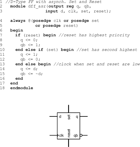
Figure 8.21 D-type flip-flop with asynchronous set and reset.
The previous two examples have shown how a sequential logic module can be described having either a single active-high or active-low asynchronous reset. The following example shows how both asynchronous reset and set inputs can be accommodated, if required.
Figure 8.21 shows the Verilog module and symbol for a D-type flip-flop having true and complementary outputs along with both a set input and a reset input for asynchronous initialization to either logic 1 or logic 0 respectively. Note that, in general, although this example makes use of only active-high control inputs, any combination of active-high and active-low control can be described by use of the posedge and negedge event qualifiers.
Lines 4 and 5 of the listing given in Figure 8.21 or together three inputs to form the event expression, one of which (clk) is the synchronous clock. This event expression, combined with the nested if…else…if…else statement, implements the hierarchical reset and set operations in conjunction with synchronous clocking. Notice the use of the begin…end bracketing to enclose the two assignments that make up each part of the if…else statement.

Figure 8.22 Example of a module using synchronous reset.
In certain situations it may be necessary, or indeed desirable, to perform all initialization synchronously. In this case, all assignments to the reg-type outputs of a sequential logic module are synchronized to the positive or negative edges of the master clock input.
The example shown in Figure 8.22 illustrates how the above can be implemented. The figure shows a Verilog module and symbol for a fully synchronous 8-bit data register. The event expression in line 5 of the listing shown in Figure 8.22 refers only to the positive edge of the Clk input. Therefore, all assignments to Dataout are subject to this condition, including the reset operation that occurs when Rst is at logic 1.
The last example in this section is a Verilog design that makes use of various aspects from previous examples, such as scalability, synchronous clocking and behavioural modelling.
Figure 8.23 shows the listing and symbolic representation for a so-called universal register/counter capable of performing a number of useful operations, in addition to having scalable input and output data ports. The latter is achieved by means of a parameter named size declared in the module header.
The module unireg, as well as being a parallel data register, is capable of performing the function of an up/down counter as well as providing left and right shifting. The number of bits that make up the register is defined by a parameter in line 2 of the listing, and, as shown, it is set to a default value of 8.

Figure 8.23 A universal counter/register module.
The dataout port of the unireg module constitutes the register itself; this is declared inline 6 of the module header. Each operation that the register performs is synchronized with the positive edges of the clock input; the nature of the operation is determined by a 3-bit control input named mode declared in line 4. The function selection nature of the mode input is implemented using a case…endcase statement between lines 10 and 22; each possible value of mode corresponds to one of the unique branches situated in lines 11–21. There are a total of seven operating modes, the last (mode = 6 or 7) being covered by the final default branch in line 21.
Serial data inputs are provided for left and right shifting, via input ports serinl and serinr respectively. With reference to the listing in Figure 8.23, lines 15–18 correspond to the shift left operation (mode = 4), where the register bits are shifted to the left by one position and the serial data present on input port serinl is loaded into bit 0 of the register. This synchronous data movement is achieved through the use of two nonblocking assignments in lines 16 and 17.
A mode value of 5 corresponds to aright shift. This corresponds to line 20 of the listing, where the concatenation operator is used to move the most significant size-1 bits into the least significant size-1 bit positions. The leftmost bit (MSB) of the register is loaded with the serial data applied to the serinr input port.
Operating modes 0 to 3 are self-explanatory; these correspond to the sequential assignments situated in lines 11–14 of the listing in Figure 8.23.
The remaining mode of operation is covered by the default branch of the case statement; this is the refresh mode, corresponding to a mode value of 6 or 7. The default sequential assignment simply assigns the register with the current value of dataout, i.e. itself. This could have been achieved in an alternative manner, as shown below:
default: ; // refresh using null statement
The null statement (;) is a ‘do nothing’ statement; in the above context it indicates that the dataout register is to retain its current value by virtue of not being updated. The choice of whether to use this method of retaining or refreshing the value stored in a reg-type signal, as opposed to the method shown in line 21, is a matter of personal preference.
The last output port of the unireg module is a wire-type signal named termcnt, which is a shortened form of ‘terminal count’. The purpose of this output is to indicate when the register has reached the maximum or minimum value when operating in count-up or count-down mode respectively.
The flexible nature of the dataout register length makes it difficult to compare it with a fixed maximum value such as 8'hFF; this problem is overcome by the use of the conditional operator and the bitwise reduction operators, as shown in the continuous assignment in lines 25 and 26 of the listing of Figure 8.23, and repeated below:
assign termcnt = (mode == 3) ? ~|dataout:( (mode == 2) ? &dataout: 0);
The above expression detects when the operating mode is either ‘count-up’ (2) or ‘count-down’ (3) and respectively assigns the reduction AND or the reduction NOR of dataout to the termcnt port. It is straightforward to appreciate that the expression will result in a logic 1 if mode is equal to 2 (3) and all of the register bits are logic 1 (logic 0), otherwise the above expression will be a logic 0.
Figure 8.24 includes a listing of a test module named Test_unireg, the purpose of which is to allow simulation of the universal register/counter described above. The module contains a declaration of a local parameter (test_size)in line 3 that is effectively a constant value for use within the enclosing module. In this case, the local parameter test_size is assigned the value 4. This corresponds to the number of bits contained in the parallel data input reg, and data output wire, connected to the register (see lines 7 and 9), as well as being used to override the value of the parameter that sets the width of the instantiated universal register/counter (size). This latter use of a local parameter, to determine the value of a parameter used in a scalable module, is implemented in line 12 of the test module shown in Figure 8.24.
The test module shown in Figure 8.24 includes two initial sequential blocks, the first of which generates a repetitive clock signal in lines 20–25 inclusive. The second initial block, spanning lines 26–49, generates a sequence of stimulus signals to exercise the various operating modes of the universal register/counter. The results of running the simulation are shown below the listing in Figure 8.24.
After clearing the register to zero by forcing the mode input to zero, the register is then set to counting-up mode (2) for 30 clock cycles. Inspection of the simulation waveforms clearly shows the data output bits counting up in binary, during which the terminal count (termcnt) output goes high coincident with a data output value of all ones.
The test module then sets the mode control to count-down mode (3) for a further 30 clock cycles. The data output bits follow a descending sequence and, as expected, the terminal count output is asserted when the state of all zeros is reached. The other operating modes of the universal register/counter are activated by subsequent statements in the initial block, shifting left (mode = 4) and shifting right (mode = 5), parallel load (mode = 1) and refresh (mode = 7) between lines 38 and 47; the simulation is stopped by the system command in line 48.
8.6 DESCRIBING MEMORIES
This section presents some very simple modules that can be used as rudimentary simulation models of RAM and ROM. These modules lack the timing accuracy and sophistication of the Verilog simulation models that are occasionally provided by commercial memory-device manufacturers. However, they can nevertheless be used effectively whenever a fast, functional model is required as part of a larger system simulation.
The Verilog descriptions discussed in this section serve to further reinforce some of the aspects that have already been covered, such as scalability and the use of parameters, as well as behavioural modelling with sequential blocks. In addition to these important elements of Verilog, the memory models presented here make use of other features not yet covered in previous chapters; these are as follows:
- arrays – the principle mechanism used to model a memory;
- bidirectional ports – the ability to use a single port as an input or output;
- memory initialization – loading a memory array with values from a file.
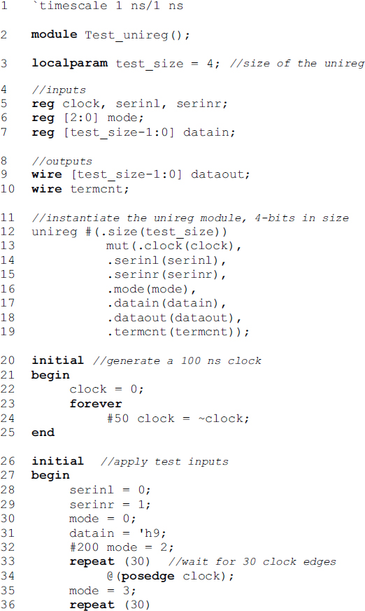
Figure 8.24 Test module and simulation results for universal register/counter.

The Verilog language does not support the creation of a new and distinct composite type such as an array or record; instead, an array of regs can be declared using the following syntax (an array of wires can be declared in a similar manner):
//An array of m, n-bit regs
reg [n-1: 0] mem[0:m-1];
The above line declares an array having m elements, each one comprising an n-bit reg. In this manner, the object named mem can be viewed as a two-dimensional array of bits, i.e. a memory.
The capabilities of the Verilog language in terms of array handling were considerably enhanced with the release of the Verilog-2001 standard, with multidimensional arrays and the ability to reference an individual bit directly being two of the key improvements. The aforementioned new features provided by the update are not required by the simple memory models presented here, however; for further information, see Reference [2].
The other feature commonly made use of in memory models is bidirectional data communication. Most RAMs make use of a bidirectional three-state data bus to allow both read and write accesses using a single set of bus wires. The Verilog language provides for this by means of the inout port mode, along with the built-in simulation support for the high-impedance state in conjunction with the resolution of multiple signal drivers. It should be noted that the inout port is modelled as a wire having one or more drivers. During a read operation, for example, the inout port is driven by the value being accessed from the memory array; otherwise it is driven to the high-impedance state. During a write operation to a RAM, the port is driven by an external source which, combined with the high-impedance value being driven onto the data bus by the memory module itself, automatically resolves to a value to be written into the memory array.
Figure 8.25 shows the symbol and Verilog description of a simple and flexible RAM module. The model is general purpose insofar as it provides scalable address and data buses, allowing different-sized memories to be instantiated.
Line 4 of the listing of the module named ram declares the parameters Awidth and Dwidth. These define the width of the address and data ports subsequently declared in lines 6 and 7 of the module header. Three active-low control signals are declared in line 5, having the following functionality:
- web – write-enable, writes data into the memory array when low;
- ceb – chip-enable, enables the memory for reading or writing;
- oeb – output-enable, drives the data from the memory array onto the data port during a read operation.
The length of the memory array is equal to the number 2 raised to the power of the number of address input bits, i.e. 2Awidth. The local parameter declared on line 8 computes this value by means of the shift-left operator (since, as mentioned previously, not all simulators support the ‘** ’ operator).
The localparam Length is then used in the declaration of the memory array in line 9 of the listing in Figure 8.25.
Lines 11 and 12 describe the logic for a memory read operation using a continuous assignment, as repeated below:
assign data = (~ceb & ~oeb & web) ?
         mem[address]: 'bz;
The above statement is executed whenever a change occurs in any of the signals on the right-hand side of the assignment operator (=); this includes all of the memory control inputs, as well as the address value.

Figure 8.25 Verilog description and symbol for a simple RAM.
The inclusion of the condition that ‘write-enable’ must be a logic 1 during a read limits the possibility of a so-called bus contention, the result of trying to perform a read and a write simultaneously.
The memory word being read is accessed using the familiar array indexing notation ([]) found in the C language and also when accessing individual bits or bit ranges of a multi-bit reg or wire.
It should be pointed out that the Verilog-1995 language does not allow part- or bit-selects to be used in conjunction with an array access, this being one of the enhancements introduced with the update resulting in Verilog-2001. This limitation does not affect the simple memory models discussed here, since all accesses to memory arrays are to whole words only.
The use of a continuous assignment in lines 11 and 12 of the listing in Figure 8.25 is consistent with the definition of the data port as mode inout, effectively making it behave as a wire. The continuous assignment will drive the bidirectional data ports of the memory module with the high-impedance state if the condition preceding the ‘?’ is false.
The memory write operation is implemented by the sequential always block in lines 14–16 of the listing in Figure 8.25. The incoming data value is latched into the memory array at the rising edge of the active-low ‘write-enable’ control input, providing the memory is enabled and not attempting to perform a read. In this case, the bidirectional data ports of the memory are being used as input wires; the Verilog simulator automatically resolves the value on the data port from the combination of the high-impedance state being assigned by the continuous assignment in lines 11 and 12 and the value being driven onto the port from the external source.
Figure 8.26 shows the Verilog source description of a test module for the ram model of Figure 8.25. An important aspect of the test module test_ram is the requirement to declare the local signal to be connected to the bidirectional data port of the ram as a wire rather than a reg, as would normally be the case if it were purely an input.
The wire named data, declared and continuously assigned in lines 9 and 10, must be driven to the high-impedance state when the memory is being operated in read mode.
In order to achieve the above, the test module makes use of a single-bit reg, named tri_cntr (short for tri-state control), to control when the data to be written, data_reg, is driven onto the bus wire data. During write operations, tri_cntr is set high to enable the data_reg values to be written to the memory array, whereas during read operations tri_cntr is forced to logic 0 with the corresponding effect of making the data bus wire high impedance.
A 16-byte RAM is instantiated in the test module in lines 35–38, by overriding the address and data width parameters with the numbers 4 and 8 respectively. The initial sequential block, starting at line 11, performs a sequence of 10 writes to the address locations 0 to 9; the data being written is an alternating sequence containing the hexadecimal values 8'h55 and 8'hAA. At the end of this sequence of writes the address is reset back to zero and the data bus wire is driven to the high impedance state by setting tri_cntr to logic 0 in line 26. The second repeat loop situated between lines 27 and 32 then performs 10 read operations from addresses 0 to 9, as above.
Figure 8.27 shows a block diagram to illustrate the structure of the test module described in Figure 8.26.
Simulation of the test-module results in the waveforms shown below the listing in Figure 8.26. As shown, the write operations occur as a result of the webar pulses being applied during the middle of each valid address and data value interval. The resulting stored values are then read out by disabling the datareg source by lowering tri_cntr, and then applying a sequence of oebar pulses while incrementing the address.
A ROM can be used wherever there is a need to store and retrieve fixed data during a simulation. For example, a set of test patterns could be stored in a ROM and subsequently used as test data (both stimulus and responses) for a module under test during the execution of a test module.
An embedded microcontroller may make use of an external ROM to store the fixed machine code program it will fetch and execute as part of a system-level simulation.
A simple Verilog model of a ROM, along with the corresponding symbolic representation, is given in Figure 8.28. In common with the RAM described above, the memory is designed to be scalable, having parameters to define the width of both the address bus and the data bus declared as part of the module header.

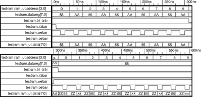
Figure 8.26 Test module and simulation results for the simple RAM.
As in the case of the RAM module of Figure 8.25, the module rom in Figure 8.28 uses a localparam to calculate the length of the memory using the number of address bits at line 6, and then goes on to declare the actual memory array at line 7. The behaviour of the model is encapsulated in a single continuous assignment in line 8 of the listing in Figure 8.28; this statement assigns the contents of the memory array mem, indexed at location address, to the data output port, providing that the output enable control input oeb is asserted. Note that, in the case of the ROM, the data output port is of mode output rather than inout, since data are only ever read from the module. With the output enable control input at logic 1, the data output is set to the high-impedance state.
The actual contents of the ROM array mem are not specified anywhere in the Verilog description shown in Figure 8.28. For this type of ROM description, the stored data are defined externally, in an ASCII text file, and loaded into the memory array at the beginning of the simulation. This method of initializing a ROM can also be used for a RAM, if required. It also provides a convenient way of loading a large amount of data into a memory from a file generated by a third-party tool, such as an assembler.

Figure 8.27 Block diagram of the module test_ram.

Figure 8.28 Verilog description of a ROM.
There are two ‘system commands’ that are available for loading a memory array from a text file:
- $readmemb( “filename”, array_name);
- $readmemh( “filename”, array_name);
The difference between the two functions lies in the format used to represent the stored data within the text file; the first function requires the data to be entered into the text file in binary, whereas the second makes use of a text file containing hexadecimal values.
Listing 8.2 shows the contents of an example text file containing binary data values for loading into a memory array. The first line specifies the numeric address, in hexadecimal format, of the starting location. This is usually equal to zero. Subsequent use of the @hex_address delimiter allows the memory to be initialized in discrete sections with different blocks of data.
@0
1010 0000 1111 1011 0010 1001 0110 1110
0111 1101 1011 1111 0000 0001 0010 0101
1010 0000 1111 1011 0010 1001 0110 1110
0111 1101 1011 1111 0000 0001 0010 0101
Listing 8.2 Contents of the file rom_data.txt.
The actual data values are listed in the order they will be stored in memory separated by white space, such as one or more space characters or the new-line character. If the number of values contained within the text file is less than the size of the memory array, then the remaining memory array locations are undefined.

Figure 8.29 Verilog test-module for the ROM.
The text file name fieldy “filename” is a valid path name to the text file containing the data. The exact format used here depends on the operating system of the computer used to perform the Verilog simulation, but generally the name of the text file is all that is required if the file is in the same location (folder or directory) as the Verilog source files that make use of it.
The call to the system commands $readmemb() and $readmemh() may be made from within the actual memory module itself, in which case the array_name field refers to the name of the memory array defined within the enclosing module, e.g. mem in the listing shown in Figure 8.28.
In the present example, the initialization of the ROM memory array is performed within the test-module Test_rom, shown in Figure 8.29. Here, an initial block in lines 6 and 7, containing a single statement, loads the binary data shown in Listing 8.2 into the memory array:
$readmemb(“rom_data.txt”, dut.mem);
As shown above, the reference to mem must be preceded by the instance name of the rom being instantiated in lines 8–11 of the listing shown in Figure 8.29. The default values of the address and data widths of the ROM are overridden such that a ‘32 × 4’ (32 words, 4-bits per word) memory is instantiated; this corresponds to the memory array values defined by the rom_data.txt file shown in Listing 8.2.
The remainder of the test module shown in Figure 8.29 corresponds to an initial block between lines 12 and 24 that reads each stored value out from the memory array, from location 0 to 31. The resulting simulation waveforms shown below the listing in Figure 8.29 illustrate this process; careful inspection of the data values output during the periods when oebar is asserted reveals that they are identical to those stored in the text file rom_data.txt.
The last example in this section on Verilog memories shows an alternative approach to describing a ROM. Listing 8.3 shows the source description of a module named rom_case. As the name suggests, this variation of a ROM makes use of the Verilog case…endcase sequential statement.
1 //read only memory using a case statement
2 module rom case #(parameter Awidth = 8, Dwidth =
3                 (input oeb,
4                 output [Dwidth-1:0] data,
5                 input [Awidth-1:0] address);

6 reg [Dwidth-1:0] data i;

7 always @(address)
8 begin
9   case (address) //define rom contents
10     0: data_i = 'h88;
11     1: data_i = 'h55;
12     2: data_i = 'haa;
13     3: data_i = 'h55;
14     4: data_i = 'hcc;
15     5: data_i = 'hee;
16     6: data_i = 'hff;
17     7: data_i = 'hbb;
18     8: data_i = 'hdd;
19     9: data_i = 'h11;
20     10: data_i = 'h22;
21     11: data_i = 'h33;
22     12: data_i = 'h44;
23     13: data_i = 'h55;
24     14: data_i = 'h66;
25     15: data_i = 'h77;
26     default: data_i = 'h0; //use `‘x’ or ‘0’
27  endcase
28 end
29 //three-state buffer
30 assign data = (oeb == 1'b0) ? data_i: 'bz;

31 endmodule
Listing 8.3 Verilog description for the ROM using a case statement.
The module header is identical to that of the module shown in Figure 8.28; this is followed by the declaration of a reg named data_i having Dwidth bits. This object acts as a signal to hold the output of the case statement, prior to being fed through the ‘three-state buffer’ at line 30.
The always block in line 7 responds to events on the input address only; the enclosed case statement then effectively maps each address value to the appropriate data value. In this manner, the ‘contents’ of the memory are explicitly defined within the module itself, rather than being contained in an external file. This may restrict this approach to the description of relatively small memories, due to having to specify each value explicitly within the module text.
Where the number of data values is less than the capacity of the memory (2Awidth), the default branch in line 26 must be included to cover the unused memory locations. A default value of x rather than zero will result in a smaller logic circuit if the ROM is to be implemented in the form of a combinational logic circuit, since an x is interpreted as a ‘don't care’ condition by a logic synthesis software tool.
8.7 DESCRIBING FINITE-STATE MACHINES
This section describes how the Verilog HDL can be used to create concise behavioural-style descriptions of FSMs. The underlying building block of many digital systems, the FSM is a vitally important part of the digital system designer's toolbox. The behavioural statements provided by Verilog facilitate the quick and straightforward creation of synchronous FSM simulation models, once the state diagram has been drawn. This, when combined with the wide availability of powerful logic synthesis software tools, makes the realization of state machines extremely efficient and rapid.
Figure 8.30 shows the block diagram structure of a general synchronous FSM. As shown in Figure 8.30, the FSM comprises two major blocks connected in a feedback configuration: the STATE REGISTER and the OUTPUT/NEXT-STATE LOGIC. There are several possible variations on the basic structure; however, the state register generally consists of a collection of n flip-flops (where 2n must be greater than or equal to the number of FSM states), and the OUTPUT/NEXT-STATE LOGIC block contains the combinational logic that predicts the next state and the output values.
Figure 8.30 General FSM block diagram.
The general block diagram shown in Figure 8.30 represents the so-called Mealy FSM, where the k output bits depend both on the n state bits and the m input bits. Initialization of the FSM may be provided through the use of an asynchronous Reset input that forces all of the state flip-flops into a known state (usually zero). One possible disadvantage of the Mealy FSM architecture is the fact that the Output can change asynchronously, in response to asynchronous changes in the Input. This can be removed by making the outputs depend only on the Present-State signal, i.e. the output of the state register. This modified structure is better known as the Moore FSM. This section will present guidelines and examples on how to construct Verilog behavioural descriptions of both Mealy and Moore FSMs.
The starting point in the design of any FSM is the state diagram. This graphical representation provides a crucially important visual description of the machine's behaviour, allowing the designer to determine the number of states required and establish the logical transitions between them. Once the number of states has been determined, the next step is to assign a unique binary code to each state; this is known as the state assignment. In Verilog, the state assignment can be defined in a number of different ways, using:
- local parameters;
- parameters declared as part of the module header;
- the `define compiler directive.
The first of these is perhaps the most obvious choice, since the state values are likely to be a set of fixed codes referenced from within the module describing the FSM. The following line of Verilog illustrates how a set of state values is defined for an FSM having four states:
From the point of the above declaration, the symbolic names s0…s3 can be used instead of the binary codes, making the description more readable.
Defining the state values as a set of in-line parameters within the module header provides the additional flexibility of being able to reassign them when the FSM module is instantiated, as shown below:
//module header with in-line parameters
module fsm # (parameter s0 = 0,
                  s1 = 1,
                  s2 = 2,
                  s3 = 3)
           (input clk, …, output…);
//overriding default parameter values
fsm #(.s0(2),
       .s1(0),
       .s2(3),
       .s3(1))
     F1(.clk (CLK), …);
The third approach makes use of the `define compiler directive in a similar manner to the way in which #define is used in the C/C++ languages to perform text substitution. The compiler directives come before the module header, as shown by the following example:
‘define WAIT 4'b001
‘define IDLE 4'b011
‘define ACK1 4'b101
‘define ACK2 4'b110

module fsm(…);
Within the body of the fsm module above, reference is made to the defined state values as follows:
//identifier must be prefixed by grave-accent character
Present-State <= ‘IDLE;
The STATE REGISTER block shown in Figure 8.30 is described by an always sequential block; therefore, the output signal it assigns to must be declared as a reg-type object, as shown below:
The typical format of the state register sequential block is shown in Listing 8.4.
1 always @(posedge Clock or posedge Reset)
2 begin
3    if (Reset == 1'b1)
4      Present-State <= s0;
5    else
6      Present-State <= Next-State;
7 end
Listing 8.4 General format of state register always block.
As described in previous sections, the sequential block shown in Listing 8.4 describes synchronous sequential logic with active-high asynchronous initialization (active-low asynchronous initialization is equally possible).
On each 0-to-1 transition of the Clock signal, the Present-State is updated by the incoming Next-State value in line 6, the latter being produced by the OUTPUT/NEXT-STATE LOGIC block. Now the Present-State signal is an input to the OUTPUT/NEXT-STATE LOGIC block; therefore, it responds to this input change, combined with the current values of the inputs, by updating the Next-State output value. The feedback signal Next-State is now ready for the next positive edge of the clock to occur, thereby updating the Present-State in a cyclic manner.
It is good practice to split the OUTPUT/NEXT-STATE LOGIC block into two separate parts, one for the outputs and another for the next state. This results in a more readable and, therefore, maintainable description. Listing 8.5 shows the outline Verilog source description for the ‘next-state’ part of this block.
1 always @(Present-State, Input1, Input2, Input3…)
2 begin
3 //consider each possible state
4   case (Present-State)
5     s0: if   (Input1 == 1'b0)
6          Next-State <= s1;
7       else
8          Next-State <= s0;
9      s1: …;
10     s2: …;
11     default: Next-State <= s0;
12   endcase
13  end
Listing 8.5 General format of next-state always block.
As shown in Listing 8.5, the next-state always block describes combinational logic; therefore, the guidelines discussed in Section 8.2 must be observed in order to ensure that Next-State is assigned a value under all possible conditions. (This is achieved in Listing 8.5 by means of the default branch in line 11.)
The always sequential block must be sensitive to changes in both the Present-State signal and all of the FSM inputs, as shown in line 1. The case…endcase statement, situated between lines 4 and 12 inclusive, considers each possible state and assigns the resulting Next-State depending on the input conditions. In this manner, the next-state part of the block describes the flow around the state machine's state diagram in terms of behavioural statements. The fact that the Next-State signal is assigned values by an always sequential block means that it must be declared in a similar manner to the Present-State signal, as follows:
reg [n-1:0] Next-State; //output of combinational behaviour
The default branch (line 11) of the case statement is required to define the behaviour of the FSM for any unused states; these states result from the fact that the number of used states may be less than the number of possible states. If the FSM finds itself in an unused state, then the safest approach is to move it directly and unconditionally to the reset state, otherwise the designer may take the slightly more risky approach of treating all unused states as don't care states, in which case the default branch would be
default: Next-State <= 'bx;
The part of the OUTPUT/NEXT-STATE LOGIC block shown in Figure 8.30 that drives the FSM outputs may be described using either an additional always block or by means of continuous assignments. The choice between these approaches depends upon the complexity of the output logic. For Moore-type FSMs, the outputs depend only on the present state; therefore, the expressive capabilities of the continuous assignment are usually adequate. The potentially more complicated output logic of a Mealy FSM may require the use of a sequential block, in which case it is important to remember to qualify the outputs as being of type reg.
The following extract illustrates the use of the continuous assignment to describe the output logic of a simple Mealy FSM:
assign Output1 = ((Present-State == s0)
                  && (Input1 == 1'b0)) | |
                  ((Present-State == s2)
                  && (Input2 == 1'b1));
Here, the output Output1 depends directly on both the present state and the inputs. A variation on the use of separate sequential blocks, for the state-register and next-state feedback logic, is to combine these in a single always block. This approach has the advantage of making the Verilog description more concise and involves combining the sequential logic behaviour shown in Listing 8.4 with the combinational logic behaviour shown in Listing 8.5, as shown in Listing 8.6.
1 …
2 reg [n-1:0] state; //single state register
3 …
4 always @(posedge clock or posedge reset)
5 begin
6 if (reset == 1)
7   state <= State0;
8  else
9    case (state)
10      State1: if (Input1 == 0)
11            state <= State2;
12          else
13            state_reg <= read1one;
14      State2: if (Input2 == 1)
15            state <= State3;
16          else
17            state <= State2;
18     …
19     default: state <= 3'bxxx
20   endcase
21 end
Listing 8.6 General format of combined state-register and next-state logic always block.
Another consequence of using a combined sequential block for the state register and next-state logic is the removal of the need for two separate reg-type signals for present state and next state. As shown in Listing 8.6, only a single declared reg named state is required in line 2; the behavioural description both assigns to (lines 7, 11, 15….) and reads from (line 9) this combined signal. The combined sequential block is triggered by positive edges on either the clock or reset input (assuming asynchronous active-high initialization is being employed). After testing for the reset condition in line 6, the behaviour is much the same as that of the next-state logic given in Listing 8.5, making use of the case…endcase statement to consider each state and input condition to implement the sequential behaviour described by the state diagram.
In effect, the statements between lines 9 and 20 of the source listing shown in Listing 8.6 describe a self-contained synchronous feedback logic system where the signal state is the output of a set of D-type flip-flops and the inputs of the flip-flops are described by the combination of the case and if…else statements.
The following example FSM designs serve to illustrate the points discussed above further. The first example is concerned with the description of an FSM to control the timers used by two people playing a game of timed chess, and the second looks at a simple combination lock with automatic locking mechanism.
8.7.1 Example 1: Chess Clock Controller Finite-State Machine
Figure 8.31 shows the block diagram of a system used by two chess players to record the amount of time taken to make their respective moves. The players, referred to as Player-A and Player-B, each have their own timer (TIMER-A and TIMER-B), the purpose of which is to record the total amount of time taken in hours, minutes and seconds for their moves since the commencement of the game.
The exact details of the timer internal operation are beyond the scope of this discussion, since we are primarily concerned with the description of the FSM that controls them. The timer control inputs, en and rst, shown in Figure 8.31, operate as follows:
- rst – when logic 1, resets the time to zero hours, zero minutes and zero seconds.
Figure 8.31 Block diagram of chess clock system.
- en – when logic 1, enables the time to increment from the current time value. When en is logic 0, the current elapsed time is held constant.

At the start of a new game, the Reset input is asserted to initialize the system and clear both timers to zero time. This is achieved by means of the Clr output of the Chess Clock FSM being driven high, thereby asserting the reset (rst) input of both timers. Each chess player has a pushbutton, which when pressed applies a logic 1 to their respective inputs, Pa and Pb, of the Chess Clock FSM. After resetting the timers, the player who is not making the first move presses their push-button in order to enable the other player's timer to commence timing.
For example, if Player-A is to make the first move, then Player-B starts the game by pressing their push-button. This has the effect of activating the Ta output of the Chess Clock FSM block shown in Figure 8.31, in order to enable TIMER-A to record the time taken by Player-A to make the first move. Once Player-A completes the first move, Player-A's button is pressed in order to stop their own timer and start Player-B's timer (Ta is negated and Tb is asserted).

Figure 8.32 State diagram for chess clock controller FSM.
For the purposes of this simulation, it is assumed that the Pa and Pb inputs are asserted momentarily for at least one clock cycle, and the potential problems resulting from switch bounce and metastability [3] may be neglected.
In the unlikely event that both players press their buttons simultaneously, the Chess Clock FSM is designed to disable both timers by negating Ta and Tb.
This will hold each player's elapsed time until play recommences in the manner described above, i.e. Player-A (Player-B) presses their push-button to re-enable TIMER-B (TIMER-A).
The state diagram for the Chess Clock FSM is shown in Figure 8.32. As shown, the FSM makes use of four states having the names shown in the upper half of the state circles. The states of the FSM outputs Ta, Tb and Clr are listed in the lower half of every state circle; those outputs preceded by ‘/’ are forced to logic 0, whereas those without ‘/’ are forced to logic 1. The presence of the output states within each of the state circles indicates that the Chess ClockFSM is of the Moore variety.
The values of the inputs, Pa and Pb, are shown alongside each corresponding state transition path (arrow) using a format similar to that used to show the state of the outputs. The movement from one state to another occurs on the rising edge of the Clock input. Where the number of transitions shown originating from a given state is less than the total number possible, the remaining input conditions result in a so-called sling, i.e. the next state is the same as the current state.
For example, the state named RunA in Figure 8.32 has two transitions shown on the diagram corresponding to the input conditions ![]() Pa, Pb
Pa, Pb![]() =
= ![]() 1, 0
1, 0![]() and
and ![]() 1, 1
1, 1![]() . The remaining input conditions,
. The remaining input conditions, ![]() Pa, Pb
Pa, Pb![]() =
= ![]() 0, 0
0, 0![]() and
and ![]() 0, 1
0, 1![]() , cause the state machine to remain in the current state; hence, there exists a sling in state RunA corresponding to the condition that the Pa input is at logic 0 and the Pb input can be either logic 0 or logic 1, the latter indicating the presence of a don't care condition for input Pb.
, cause the state machine to remain in the current state; hence, there exists a sling in state RunA corresponding to the condition that the Pa input is at logic 0 and the Pb input can be either logic 0 or logic 1, the latter indicating the presence of a don't care condition for input Pb.
The asynchronous, active-high Reset input forces the FSM directly into the state named Stop, irrespective of any other condition.
The FSM depicted visually by the state diagram shown in Figure 8.32, is described in a behavioural style by the Verilog HDL listing given in Listing 8.7.
1 module chessclkfsm(input reset, Pa, Pb, clock,
2                  output Ta, Tb, Clr);

3 //ascending state assignment
4 localparam RunA = 0, RunB = 1, Stop = 2, Wait = 3;

5 reg [1:0] state;

6 //combined state register and next state sequential block
7 always @(posedge clock or posedge reset)
8   begin
9     if (reset)
10       state <= Stop;
11    else
12       case (state)
13         RunA:
14           casex ({Pa, Pb})
15             2'b0x: state <= RunA;
16             2'b10: state <= RunB;
17             2'b11: state <= Wait;
18           endcase
19         RunB:
20           casex ({Pa, Pb})
21             2'bx0: state <= RunB;
22             2'b01: state <= RunA;
23             2'b11: state <= Wait;
24            endcase
25           Stop:
26             case ({Pa, Pb})
27               2'b00: state <= Stop;
28               2'b01: state <= RunA;
29               2'b10: state <= RunB;
30               2'b11: state <= Wait;
31              endcase
32             Wait:
33               if (Pa == Pb)
34                state <= Wait;
35               else if (Pa == 1'b1)
36                state <= RunB;
37               else
38                state <= RunA;
39     endcase
40 end

41 //Moore output assignments depend only on state
42 assign Ta = state == RunA;
43 assign Tb = state == RunB;
44 assign Clr = state == Stop;

45 endmodule
Listing 8.7 Verilog description of the Chess Clock FSM.
The module chessclkfsm makes use of a local parameter to define the state values. Each state name shown in the state diagram of Figure 8.32 is assigned a value in line4. This is followed by the declaration of a 2-bit reg to hold the state of the FSM; this description makes use of the single always block approach outlined in Listing 8.6.
The sequential always block spanning lines 7–40 of the listing shown in Listing 8.7 describes the state register and next-state logic. The presence of a don't-care condition in one of the state transitions for states RunA and RunB suggests the use of a special variation of the case statement known as casex.
The use of casex instead of case in lines 14 and 20 allows the explicit use of the ‘don't-care’ value (x) within the literals specified in lines 15 and 21. In effect, this means that one or more of the inputs can be either logic 0 or logic 1, e.g. lines 14 and 15 are equivalent to the following:
14 case ({Pa,Pb})
15   2'b00, 2'b01: state <= RunA;
16 …
The case statement considers each possible value of state; in this example there is no requirement for a default branch, since the number of states is equal to a power of 2. State Stop has four unique next states, hence the need for a nested case…endcase statement with four branches, or limbs, situated in lines 27–30 inclusive. The case statement gives equal priority to each of the individual limbs or branches enclosed within the bounds of case…endcase; hence, the matching expressions must be nonoverlapping or mutually exclusive. As seen previously, multiple values may be specified on a single branch, so long as none of these values appears within any other of the branches within the statement.
The next-state behaviour of the Wait state is described using a nested if…else statement in order to illustrate the flexibility of the Verilog language. It is straightforward to appreciate that the semantics of the statement in lines 33–38 inclusive of the source description in Listing 8.7 are equivalent to the state transitions shown on the state diagram of Figure 8.32, bearing in mind that there is a sling condition corresponding to input values ![]() Pa, Pb
Pa, Pb![]() =
= ![]() 0, 0
0, 0![]() and
and ![]() 1, 1
1, 1![]() .
.
It should be noted that, despite the priority implied by the nested if…else…if statement semantics, the circuitry resulting from synthesis of this description will not include any prioritized logic. This is due to the fact that the conditions specified in each part of the if…else statement are mutually exclusive.
The outputs Ta, Tb and Clr, of the Chess Clock FSM, are of the Moore variety, i.e. dependent on the state of the machine only. These are generated by means of the continuous assignments in lines 42–44 of the source description shown in Listing 8.7. Each output is generated by continuously comparing the value of the state-register state with the local parameter value corresponding to the state in which the output is asserted.
In this simple example, each output is asserted in only one state; therefore, the logic of the outputs amounts to little more than a single AND gate.
The output logic can be further simplified by encoding the states of the FSM with values that match the outputs. In the present example, the output values are unique for each state, so this would involve simply defining the state values to be the same as the output values, i.e. replace the local parameter declarations with those shown in lines 4–7 of Listing 8.8.
3 //state assignment matches outputs Ta, Tb, Clr
4 localparam RunA = 3'b100,
5      RunB = 3'b010,
6      Stop = 3'b001,
7      Wait = 3'b000;

8 reg [2:0] state; //no. of state bits = no. of outputs

  …
39   default: state <= 3'bx;
40 endcase
   …
41 //outputs are equal to state bits
42 assign Ta = state [2];
43 assign Tb = state [1];
44 assign Clr = state [0];
Listing 8.8 Alternative state assignment to match outputs.
The output continuous assignments, situated in lines 42–44 of the listing given in Listing 8.7, would be replaced by the corresponding lines shown in Listing 8.8. As shown, each output is now mapped directly to the corresponding bit of the state register.
Another consequence of modifying the state assignments, as described above, is the need to change the number of state bits to match the number of outputs. The replacement state-register declaration, in line 8 of Listing 8.8 now declares a register having 3-bits; therefore, the next-state behaviour must be modified by the addition of a default branch in line 39, so that the additional (23 – 4 = 4) unused states are covered by the case statement.
Simulation of the Chess Clock FSM module chessclkfsm is achieved by means of the simple test module shown in Figure 8.33. The resulting timing waveforms are also shown in Figure 8.33, where the relationship between the inputs, state and outputs can be seen to follow that defined by the state diagram. Most Verilog simulation tools provide a facility whereby the values of the state waveform can be displayed in terms of the state names used on the state diagram, as is the case here. This is a significant visual aid when attempting to analyse, understand and verify the behaviour of an FSM using simulation.

Figure 8.33 Test module and simulation waveforms for chess clock FSM.
8.7.2 Example 2: Combination Lock Finite-State Machine with Automatic Lock Feature
The second example of an FSM-based design is a rather more complex system that makes use of several modules, both combinational and sequential. This example also serves to illustrate the interaction of an FSM with other synchronous sequential modules, all described in a behavioural style and clocked by a common clock signal.
Figure 8.34 shows the block diagram of a so-called ‘digital combination lock’ system. At the heart of the system there is an FSM, labelled CONTROLLER in the figure, the function of which is to detect when a user has entered the correct four-digit secret code via the Key Pad Switches, shown at the left-hand side of Figure 8.34.
The user sees a keypad with eight active-low push-button switches (SW[0]…SW[7]). The first four (SW[0…3]) are hardwired into the system via a four-to-one multiplexer; these represent the code switches. It is up to the user to connect the multiplexer inputs to the keypad switches corresponding to the secret code; in this manner, the secret access code is hardwired into the system.
The eight-input AND gate, connected to all of the switches in Figure 8.34, provides an output named allsw that goes to logic 0 if any switch is pressed. The output of the four-to-one multiplexer, named mux_out, will go to logic 0 if the switch being pressed corresponds to the multiplexer select address input sel[0..1]. In this manner, the multiplexer is able to select each switch in the code in sequence; the output mux_out will go low only if the correct switch has been pressed.
The input push-button switches are asynchronous inputs by nature, whereas the combination lock system operates entirely synchronously. It is impossible to predict for how long any pushbutton will be pressed; therefore, the duration of the logic 0 pulses coming into the system on signals mux_out and allsw is entirely unpredictable. If the aforementioned signals were fed directly into the FSM, then a single key depression lasting 0.5 s, for example, would be interpreted as a sequence of approximately n inputs, where
n = 0.5/clock_period.
The above problem is overcome by means of the simple ‘edge detector’ circuit shown in Figure 8.35. The system makes use of two of these circuits, labelled DET1 and DET2 in Figure 8.34. As shown in Figure 8.35, the circuit is essentially a synchronous 2-bit shift register with the output of the first flip-flop ANDed with the inverse of the output of the second flip-flop.

Figure 8.34 Block diagram of combination lock system.
Figure 8.35 Logic diagram of edge detector edgedet.
This simple circuit performs both synchronization and edge detection, in that it produces a single clock-cycle-length logic 1 pulse at the output named detected, near to the point when the input, edge_in, undergoes a logic 1 to logic 0 transition, regardless of how long edge_in remains at logic 0.
Neglecting the usual problems of metastability [3], which result whenever there is a need to interface between asynchronous and synchronous domains, the logic circuit of Figure 8.35 provides an effective means of interfacing the push-button switches to the FSM.
The outputs, codesw and anysw, of the two edge detectors feed directly into the FSM LOCKFSM. The fact that the edge detectors and the FSM are clocked by the same signal ensures synchronization between the two separate modules such that if a key is pressed, and it is the correct key (i.e. the four-to-one multiplexer is selecting the key), the lockfsm receives a logic 1 pulse on both codesw and anysw during the same clock cycle. The arrival of the two pulses indicates the correct key was pressed and the FSM then advances to the next state.
The Verilog descriptions of the D-type flip-flop and the edge detector are shown in Listings 8.9 and 8.10 respectively.
1  module dff(output reg q, input d, clk);

2  always @(posedge clk) q <= d;

3  endmodule
Listing 8.9 Verilog source description of D-type flip-flop.
1  module edgedet(input edge_in,
2             output detected,
3            input clock);

4  wire q0, q1;

5  dff dff0(.q(q0), .d(edge_in), .clk(clock));
6  dff dff1(.q(q1), .d(q0), .clk(clock));

7  assign detected = q0 & ~q1;

8  endmodule
Listing 8.10 Verilog source description of edge detector.
The block diagram of Figure 8.34 includes a timer module (TIMER) labelled T1. This module interfaces with the FSM via signals entimer (enable timer) and timeout (timer timed out) and is clocked by the same master clock as the FSM and edge detectors, ensuring synchronization.
The function of the timer is to provide an automatic locking mechanism, returning the system to the locked state after a delay of 30 s subsequent to the system entering the unlocked state.
The master clock signal is intended to have a frequency of 10 Hz, so the timer implements the required delay by counting to 30010, as shown in the Verilog source description shown in Listing 8.11.
1  module Timer(input Clock, Start, output Timeout);
2  //time delay value in clk pulses
3  localparam NUMCLKS = 300;

4  reg [8:0] q;
5  always @(posedge Clock)
6  begin
7     if (!Start||(q == NUMCLKS))
8        q <= 9'b0;
9     else
10       q <= q + 1;
11 end
12 //decode counter output
13 assign Timeout = (q == NUMCLKS);

14 endmodule
Listing 8.11 Verilog source description of automatic lock timer.
The Timer module behaviour is entirely synchronous: with the input named Start at logic 0, the timer is disabled and the count q held at zero.
The FSM starts the timer when it enters the unlocked state by asserting entimer (connected to timer input Start), this allows the count q to increment on each clock edge until it reaches the terminal value NUMCLKS (30010), at which point the Timeout output of the timer goes high for one clock cycle and the count returns to zero.
The FSM responds to the logic 1 on its timeout input by returning to state s0, where the locked output returns high. By returning to state s0, the FSM also negates the entimer output, thereby disabling the timer until the next time it is required.
The remaining module, as yet not discussed, in the block diagram of Figure 8.34, is the seven-segment decoder named SEGDISP. This module is purely combinational and drives an active-low seven-segment display unit that displays the state of the system, based on the values of the alarm and locked outputs of the FSM: ‘L’ for locked, ‘U’ for unlocked and ‘A’ for alarm. The Verilog behavioural description of the module is given in Listing 8.12.
1  module segdisp(input locked, alarm,
2             output SA,SB,SC,SD,SE,SF,SG);

3  reg [6:0] seg;

4  always @(locked or alarm)
5  begin
6    if (alarm == 0)
7         seg = 7'b0001000; //display ‘A’
8    else if (locked == 0)
9         seg = 7'b10 00001; //display ‘ U’
10   else
11        seg = 7'b1110001; //display ‘L’
12 end

13 assign {SA, SB, SC, SD, SE, SF, SG} = seg;

14 endmodule
Listing 8.12 Verilog source description of seven-segment display decoder.
Figure 8.36 shows the state diagram for the lockfsm module at the heart of the combination lock system.
The FSM is initialized by asserting the asynchronous reset input, this forces it into state s0, where the locked and alarm outputs are both at logic 1, indicating the system is locked and not in a state of alarm (alarm is active-low). The 2-bit selsw output of the lockfsm is set to zero, thereby selecting the first input push-button in the sequence via the four-to-one multiplexer. The timer is disabled on account of entimer being at logic 0.
What happens next depends on which of the eight push-button switches is pressed. If the first switch in the code sequence is pressed (SW[0]), then the input signals codesw and anysw go high simultaneously, causing the FSM to move into state s1, where it remains until a subsequent key is pressed.
In state s1 the selsw output of the FSM is set to 1, thereby selecting the second input of the multiplexer, this being connected to the second switch in the code sequence, SW[1]. Pressing SW[1] in state s1 asserts both codesw and anysw again, advancing the FSM into state s2.
On entering state s2, the FSM changes selsw to 2, thereby selecting the third input of the multiplexer, this being connected to the third switch in the code sequence, SW[2].
In a similar manner to that described above, pressing switches SW[2] followed by SW[3] causes the lockfsm to enter the unlock state, having pressed all four keys (SW[0]…SW[3]) in the correct order. The locked output goes to logic 0 and the seven-segment display shows the letter ‘U’.
As shown in Figure 8.36, the entimer output of the FSM is now asserted, thereby enabling the timer. The lockfsm will remain in the unlock state for as long as the timeout input remains at logic 0 (assuming the asynchronous reset input is not asserted).
As discussed above, this corresponds to a duration equal to 30010 clock periods or 30 s, whereupon the FSM will return to state s0 and reassert the locked output.
In any of the lockfsm states (s0, s1, s2 and s3), pressing the incorrect key pad switch will result in a pulse arriving from anysw, via the eight-input AND gate, but there will be no such pulse on codesw, due to the fact that the currently selected multiplexer input will not be asserted low.
Figure 8.36 Combination lock FSM (lockfsm) state diagram.
The state diagram of Figure 8.36 shows that, under these circumstances, the FSM will move to state wrong, indicating that the incorrect key was pressed. In this particular state, the active-low alarm output is asserted and the display unit outputs the code for the letter ‘A’.
The absence of any transitions leaving state wrong indicates the presence of an unconditional state transition leading from the wrong state back to itself (a ‘sling’), i.e. the only way to exit the alarm state is to force an asynchronous reset. Needless to say, the clear input would, therefore, have to be located in a secure environment, enabling only a qualified operator to reset the alarm.
The Verilog behavioural description of the lockfsm module is shown in Listing 8.13.
1 module lockfsm(input clock, reset,
2      codesw, anysw,
3            output reg [1:0] selsw,
4            output locked, alarm, entimer,
5            input timeout);

6  localparam s0 = 3'b000, s1=3'b001, s2 = 3'b010,
7            s3=3'b011,
8            wrong=3'b100, unlock=3'b101;

9  reg[2:0] lockstate;

10 always @(posedge clock or posedge reset)
11 begin
12 if (reset == 1'b1)
13    lockstate <= s0;
14 else
15    case (lockstate)
16        s0 : if (anysw & codesw)
17           lockstate <= s1;
18        else if (anysw)
19           lockstate <= wrong;
20        else
21           lockstate <= s0;
22      s1 : if (anysw & codesw)
23           lockstate <= s2;
24      else if (anysw)
25           lockstate <= wrong;
26      else
27           lockstate <= s1;
28    s2: if (anysw & codesw)
29           lockstate <= s3;
30      else if (anysw)
31           lockstate <= wrong;
32      else
33           lockstate <= s2;
34   s3: if (anysw & codesw)
35           lockstate <= unlock;
36      else if (anysw)
37           lockstate <= wrong;
38      else
39           lockstate <= s3;
40   wrong: lockstate <= wrong;
41   unlock: if (timeout)
42           lockstate <= s0;
43     else
44           lockstate <= unlock;
45     default: lockstate <= 3'bx;
46 endcase
47 end

48 always @(lockstate)
49 begin
50  case(lockstate)
51            s0: selsw = 0;
52            s1: selsw = 1;
53            s2: selsw = 2;
54            s3: selsw = 3;
55            wrong: selsw = 0;
56            unlock: selsw = 0;
57            default: selsw = 2'bx;
58    endcase
59 end

60 assign locked = (lockstate == unlock) ? 0: 1;
61 assign alarm = (lockstate == wrong) ? 0: 1;

62 assign entimer = (lockstate == unlock) ? 1: 0;

63 endmodule
Listing 8.13 Verilog source description of combination lock FSM.
In common with the previous example, this FSM is of the Moore type; therefore, the always sequential block starting at line 10 describes the state register and next-state behaviour only.
The output logic is captured by the combinational always block situated in lines 48–59 inclusive, and the continuous assignments on lines 60–62. The 3-bit state register lockstate is declared in line 9 and the six used states are assigned ascending numbers by means of a local parameter starting in line 6.
The two unused states are exploited as don't-care states by means of the default branches in lines 45 and 57 of the source shown in Listing 8.13.
All of the used states, with the exception of state wrong, make use of the if…else statement to describe the state transition logic defined by the state diagram of Figure 8.36. For example, the next-state behaviour for state s1 is repeated below:
s1 : if (anysw & codesw)
        lockstate <= s2;
     else if (anysw)
        lockstate <= wrong;
     else
        lockstate <= s1;
The first condition to be tested is the expression anysw & codesw; this will be true (logic 1) if both anysw and codesw are at logic 1. If this is the case, then the state of the FSM is moved to s2. If the first condition is false, then this leaves the possibility of either input being high or both inputs being low. The structure of the logic means that codesw cannot be high if anysw is low, so it is only necessary to test the state of anysw to see whether an incorrect key was pressed and, hence, move to the alarm state.
If no keys are pressed, then the FSM state remains the same, i.e. in this case s1. This is achieved by means of the final, and optional, else part of the above statement.
The complete combination lock system block diagram, shown in Figure 8.34, is described by the Verilog source given in Listing 8.14.
1  module comblock(input clock, clear,
2              input [7:0] switches,
3              output alarm, locked,
4              output SA, SB, SC, SD, SE, SF, SG);

5  wire mux_out, anysw, codesw,
6          allsw, entimer, timeout;

7  wire [1:0] selsw;

8  //4-to-1 multiplexor
9  assign mux_out = selsw == 0 ? switches [0]:
10             (selsw == 1? switches[1]:
11             (selsw == 2? switches[2]:
12             (selsw == 3? switches [3]: 1'b0)));

13 //AND gate for all switches
14 assign allsw = &switches;

15 edgedet det1(.edge_in(mux_out),
16            .detected(codesw),
17            .clock(clock));

18 edgedet det2(.edge_in(allsw),
19            .detected(anysw),
20            .clock(clock));

21 Timer t1(.Clock(clock),
22            .Start(entimer),
23            .Timeout(timeout));

24 lockfsm controller(.clock(clock),
25             .reset(clear),
26             .codesw(codesw),
27             .anysw(anysw),
28             .selsw(selsw),
29             .locked(locked),
30             .alarm(alarm),
31             .entimer(entimer),
32             .timeout(timeout));

33 segdisp sg1(.locked(locked),
34            .alarm(alarm),
35            .SA(SA),
36            .SB(SB),
37            .SC(SC),
38            .SD(SD),
39            .SE(SE),
40            .SF(SF),
41            .SG(SG));
42 endmodule
Listing 8.14 Verilog source description of complete combination lock system.
The comblock module comprises instantiations of the modules discussed previously, along with two continuous assignments, situated in lines 9 and 14, to implement the four-to-one multiplexer and the eight-input AND gate respectively.
Simulation of the combination lock system is achieved with the use of a Verilog test module named test_comblock, shown in Listing 8.15.
1  ‘timescale 1 ms / 1 ms
2  module test_comblock();

3  // Inputs
4  reg clock;
5  reg clear;
6  reg [7:0] switches;

7  // Outputs
8  wire alarm;
9  wire locked;
10 wire SA, SB, SC, SD, SE, SF, SG;

11 // Instantiate the combination lock
12 comblock UUT(
13             .clock(clock),
14             .clear(clear),
15             .switches(switches),
16             .alarm(alarm),
17             .locked(locked),
18             .SA(SA), .SB(SB),.SC(SC),
19             .SD(SD),.SE(SE),.SF(SF),. SG(SG)
20             );

21 initial
22 begin
23    clock = 1'b0;
24    forever
25       #50 clock = ~clock;
26 end

27 initial
28 begin
29     clear = 1'b1;
30     switches = 8'b11111111;

31     repeat (3) @(negedge clock);
32     clear = 1'b0;

33     repeat (3) @(negedge clock);
34     switches[0] = 1'b0;

35     repeat (2) @( negedge clock);
36     switches[0] = 1'b1;

37     repeat (3) @(negedge clock);
38     switches[1] = 1'b0;

39     repeat (2) @(negedge clock);
40     switches[1] = 1'b1;

41     repeat (3) @(negedge clock);
42     switches[2] = 1'b0;

43     repeat (2) @(negedge clock);
44     switches[2] = 1'b1;

45     repeat (3) @(negedge clock);
46     switches [3] = 1'b0;

47     repeat (2) @(negedge clock);
48     switches [3] = 1'b1;

49     repeat (400) @( negedge clock); //wait for timeout

50     clear = 1'b1;

51     repeat(4) @( negedge clock);
52     clear = 1'b0;
53     repeat(3) @(negedge clock);
54     switches[0] = 1'b0;

55     repeat(2) @(negedge clock);
56     switches[0] = 1'b1;

57     repeat(3) @(negedge clock);
58     switches [5] = 1'b0;

59     repeat(2) @(negedge clock);
60     switches [5] = 1'b1;

61     repeat(3) @(negedge clock);
62     switches[2] = 1'b0;

63     repeat(2) @(negedge clock);
64     switches[2] = 1'b1;

65     repeat(3) @(negedge clock)
66     switches[3] = 1'b0;

67     repeat(2) @(negedge clock)
68     switches[3] = 1'b1;

69     repeat(4) @(negedge clock)
70     clear = 1'b1;

71     repeat(4) @(negedge clock);

72     $stop;
73 end

74 endmodule
Listing 8.15 Verilog source description of combination lock system test module.
The test-module generates a 10 Hz clock using an initial sequential block starting at line 21.

Figure 8.37 Combination lock simulation showing: (a) application of correct switch sequence; (b) automatic locking feature; (c) incorrect key input sequence.

A second initial block, starting at line 27, exercises the combination lock by applying the correct sequence of switch inputs in order to reach the unlock state. This is followed by a 40 s delay, implemented using a repeat loop, to allow observation of the automatic lock feature. Finally, after resetting the system, an incorrect sequence of switches is applied in order to verify the operation of the alarm state.
Figure 8.37a–c shows a selection of simulation waveforms obtained as a result of running the test-module simulation.
REFERENCES
1. Ciletti MD. Modeling, Synthesis and Rapid Prototyping with the Verilog HDL. New Jersey: Prentice Hall, 1999.
2. Ciletti MD. Advanced Digital Design with the Verilog HDL. New Jersey: Pearson Education, 2003 (Appendix I – Verilog-2001).
3. Wakerly JF. Digital Design: Principles and Practices, 4th edition. New Jersey: Pearson Education, 2006 (Metastability and Synchronization, Section 8.9).