
9
Asynchronous Finite-State Machines
9.1 INTRODUCTION
Most FSM systems are synchronous; that is, they make use of a clock to move from one state to the next. Using a clock to control the synchronous movement between one state and the next allows the FSM logic time to settle before the next transition and, hence, overcomes some logic delay problems that may arise. For this reason, synchronous systems are, by far, the most popular in digital electronics; and most HDLs used to define them are optimized for synchronous system design.
However, there is another kind of FSM, one that does not use a clock to instigate a transition between states. This is knows as the asynchronous FSM. In an asynchronous FSM, the transition between states is controlled by the event inputs, so that the FSM does not need to wait for a clock signal input. For this reason, asynchronous FSM are sometimes called ‘event-driven’ FSMs.
A typical event FSM is shown in Figure 9.1. In this FSM, the transition from state s0 to s1 will take place when input s is logic 1 AND input c is logic 0. On reaching state s1, the FSM will remain in this state until the input c goes to logic 1, at which point it will move to state s2. Here, it will remain until input c goes to logic 0 to move to state s3, before returning to state s0 when input s goes to logic 0.
In this example, the FSM will only change state when there is a change of input variable; hence, the event nature of the system.
Sometimes, it is desired to change state when there is no input signal change (as has been seen in clocked driven systems).
In Figure 9.2, the transition between s3 and s0 does not have an input term along the transitional line. This implies that when the FSM reaches state s3 (when input x became logic 1) the FSM will move to s0. The time taken for the FSM to move to s0, when it reaches state s3, will be determined by the propagation delay of the event logic used in the system. This will be as fast as the logic technology used to implement the design.
An important feature with event-driven FSM systems is that when the FSM is in a stable state (perhaps waiting for an input event to move to the next state) the power drain is very low in CMOS circuits, since there is no repetitive clock to consume power. This allows asynchronous (event) systems to be low power, while also being very fast. This latter point is due to the fact that the event FSM will move to the next state as soon as the relevant event input changes, and is only limited by the propagation delay for its event-driven logic.
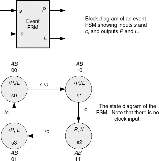
Figure 9.1 Example of an asynchronous FSM.
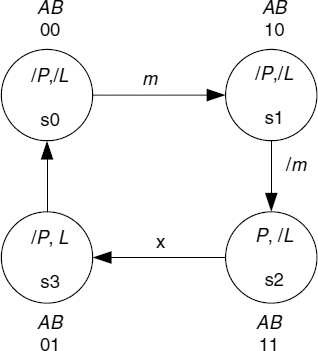
Figure 9.2 Transition without an input event.
9.2 DEVELOPMENT OF EVENT-DRIVEN LOGIC
From the previous section it is clear that an event state diagram can be developed in much the same way as a clocked driven state diagram. However, whilst with a clocked FSM, the implementation (synthesis) will make use of some type of flip-flop (D type, T type, or JK type), the event-driven system needs to make use of memory elements that do not require a clock input. This implies that perhaps SR latches are required. But in practice these latches may, in some cases, need multiple set (s) and multiple reset (r) inputs. What follows is the development of a set of equations that can be used to implement a general ‘event-driven’ cell for each particular application.
Consider Figure 9.3. This shows the block diagram for the proposed event cell. This cell has a ‘turn-on set’ input to set the cell output to logic 1, a ‘turn-off set’ to turn the cell output to logic 0, and a hold term input, derived from the cell output to hold the cell either in its set, or rest state.
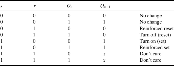
In order to develop the logic equations for the event cell a table of required states for each input condition is required. This is shown in Table 9.1. In this table, the ‘turn-on set’ input is denoted as s, the ‘turn-off set’ is denoted as r, the current state of the cell output is Qn, and the next state of the cell output is Qn+1. The two inputs s and r, together with the current output state, are shown as a binary sequence. This defines all possible states for the cell. What is now required is to fill in the required state condition for each Qn+1 state.
- In row 1, s = r = 0, and the cell is currently reset. Since our event cell is to remain in whatever state it happens to be in, when s = r = 0, then Qn+1 = Qn = 0.
- In row 2, s = r = 0, but the cell is currently set. Therefore, Qn+1 = 1, since the cell must remain in the set state.
- In row 3, s = 0 but r = 1, implying a reset condition for the event cell. Since the cell in this row is currently reset, then Qn+1 = 0 as well.
- In row 4, s = 0, r = 1 as before, but the cell is currently set, so the required action is that Qn+1 = 0 to reset the cell.
Figure 9.3 The event cell.
Table 9.1 State table for the event cell.a
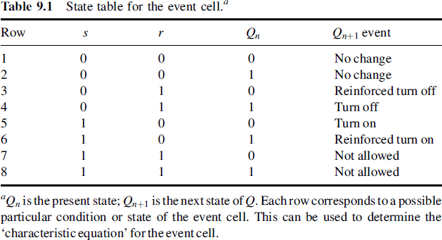
- Moving to row 5, s = 1 and r = 0. The cell is currently reset; thus, Qn+1 = 1 to set the cell.
- In row 6, s = 1 and r = 0 as before, and the cell is currently set; therefore, Qn+1 = 1 to hold the cell in its set state.
- In rows 7 and 8, both s = 1 and r = 1. This is not a very practical condition for the cell, since it implies that the cell inputs are ambiguous (i.e. set the cell and reset the cell at the same time!). Clearly, this is impossible. Here, our own common sense will prevail, and both rows 7 and 8 are defined as ‘not allowed’ states. What is meant here is that it is rather hoped that the input conditions defined by rows 7 and 8 ‘won't’ happen. This is usually referred to as ‘don't care’ states. It is important that the ‘don't care’ does not happen, and this will be assumed in the design of asynchronous systems that use the corresponding equations being developed here. The input conditions s = 1 and r = 1 will not be allowed to occur. This is not too difficult to ensure, so one marks out the row 7 and 8 Qn+1 outputs with x.
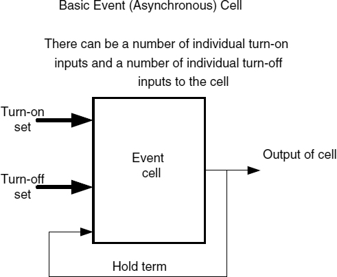
Table 9.2 illustrates the completed table.
Now, an equation for Qn+1 can be developed from this table in terms of s, r, and Qn:
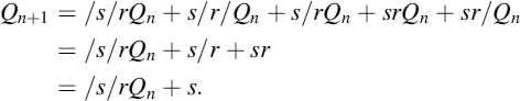
Table 9.2 Completed state table for the event cell.
Applying the auxiliary rule and rearranging results in the following sequential equation:
Qn+1 = s + Qn/r.
The sequential equation produced here represents the ‘characteristic equation’ for the event cell. Notice that in line 3 the ‘don't care’ terms s/r + sr have been reduced to the term s.
The sequential equation can be stated as:
The new output state for the event cell is equal to the condition of the set input s or the current state of the cell Qn and the inverse of the reset input r.
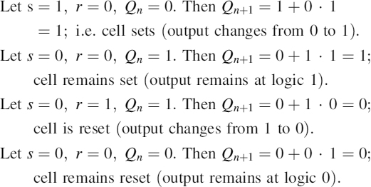
This can be easily proved, as shown below, by defining initial states for s, r, and Qn using the sequential equation to predict the new output Qn+1. Note that, in these equations, the r term is /r, so r = 0 means /r = 1, and r = 1 means /r = 0.
As it stands, the sequential equation is rather limited because it caters for only a single input s term and a single input r term. In real event-driven systems there may be a requirement for multiple set and multiple reset terms so that the cell can be set and reset under different conditions. But these will be OR terms, since the state diagram is sequential and can only deal with one set and one reset condition at a time. So the sequential equation can be modified by introducing the possibility of multiple set inputs as:
Sum of set inputs ∑s = s1 + s2 + ··· + sn, where sn is the final set input term.
Sum of reset inputs ∑r = r1 + r2 + ··· + rn, where rn is the final rest input term.
Thus, the sequential equation becomes:
This is the final form of the sequential equation used to define the event cell. It is referred to as the NAND sequential equation [1].
Note that there is a corresponding equation called the NOR sequential equation that is defined as
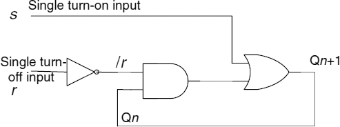
Figure 9.4 Basic event cell.
But it is not used much these days. You may like to try to see how this NOR sequential equation is obtained from the sequential equation. (Hint: AND (∑rQ + ∑/rQ) with the ∑sQ and expand.)
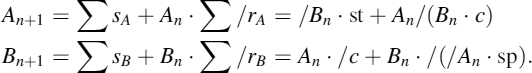
Equation (9.1) can be described for an event cell A as
A = ∑(turn-on sets of A) · A + ∑/(turn-off sets of A)
and Equation (9.2) as
A = (∑(turn-on sets of A) + A) · ∑/(turn-off sets of A).
Both these equations were used in the book Problems and Solutions in Logic Design by D. Zissos [1] (chapter 1: ‘Basic concepts in logic design’) and are repeated here by permission of Oxford University Press.
The next stage is to show how the sequential equation can be used to synthesize an event FSM. This will be followed by an example of how to design an event-driven FSM from a specification.
Returning to the sequential equation, Equation (9.1), a circuit can be produced. This is shown in Figure 9.4.
Qn+1 = s + Qn · /r.
This is the equation defining the circuit of Figure 9.4. This can be converted into NAND form by applying De Morgan's rule to obtain:
This is where the ‘NAND’ sequential equation name comes from. The event cell circuit is shown in Figure 9.5.
Either type can be used in practice, although with PLD and FPGA devices the AND/OR arrangement fits best.
9.3 USING THE SEQUENTIAL EQUATION TO SYNTHESIZE AN EVENT FINITE-STATE MACHINE
The event state diagram shown in Figure 9.6 will be used to synthesize an event system. The design process for event state diagrams will be dealt with later. The system is essentially able to determine a 0 to 1 transition on the c input.
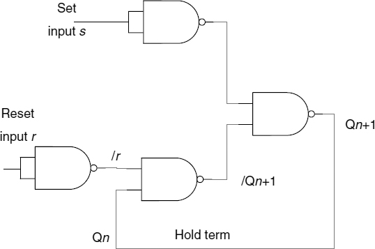
Figure 9.5 Event cell circuit.
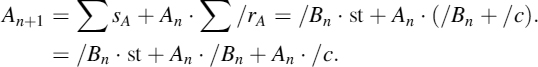
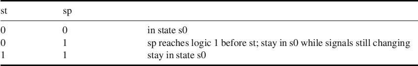
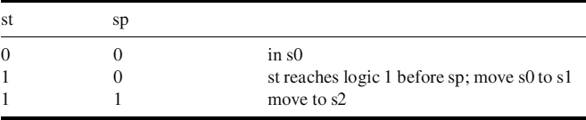
In this system there are three inputs: st, c, and sp. There is a single output P that is logic 1 in state s3. Note that there are two event cells in this state diagram: event cell A and event cell B. These form the secondary state variables.
When the operator asserts input st, the system moves from state s0 to s1, where it waits for the input c (the incoming pulse) to become logic 0 (if c is logic 0 in state s0, then the FSM will simply move through s1 to s2). When the FSM reaches s2 the system waits for c going high. In this way, the event-driven system is able to catch the positive-going transition on input c. The P output will remain high until the sp input is asserted. In this way, the P output acts as a memory of the transition event on c.
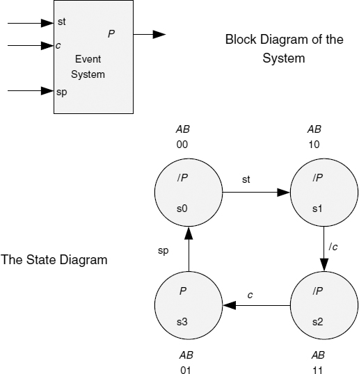
Figure 9.6 The basic event-driven system.
When the operator asserts input sp, the FSM will move back to state s0.
This system can be left unattended, since it will indicate the c 0 to 1 transition, and asserting sp will allow the operator to return the system to its initial state again. Note that the system can be reset to s0 via its reset input as well (not shown).
First, the turn-on set of conditions to set the A event cell must be determined.
The ∑sA is found by looking for the state where An goes from 0 to 1. This is state s0, for An = 0 in state s0, and An = 1 in state s1. There is an input along the transitional line between s0 and s1, so this input st is included in the turn on set for An. Therefore:
The reason why s1 · st is needed is because the input st must still be logic 1 (active) when the FSM reaches state s1 to ensure that it will remain in this state.
Now:
∑sA = /An · /Bn · st + An · /Bn · st = (/An · /Bn + An · /Bn) · st = /Bn · st
due to the application of the logical adjacency rule. Note: this has effectively led to the removal of the An term in the equation for the turn-on set for event cell An.
Now, looking for the turn-off condition, this occurs in state s2 when An is changing from 1 to 0. Therefore:
since the c input must be held true in state s3 to ensure that the event cell hold reset. In terms of the state variables:
∑rA = AnBn · c + /An · Bn · c = (An · Bn + /An · Bn) · c = Bn · c.
The An term is removed by the logical adjacency rule to leave the Bn and c terms. This results in the turn-off term
∑rA = Bn · c.
The complete sequential equation can now be written thus:
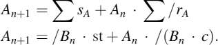
This represents the required behaviour for the event cell A. It is the sequential equation for the event cell A originally called the NAND sequential equation by Professor D. Zissos in his book Problems and Solutions in Logic Design [1].
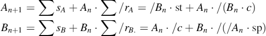
The sequential equation for the event cell B can be obtained in the same way:
Bn+1 = ∑sB + Bn · ∑/rB.
The turn-on set for B is
Note here that the application of the logical adjacency rule has removed the Bn term in the same way that the An term in the turn on set equation for A was dropped.
The turn-off set for B is
Likewise, the Bn term is dropped using the logical adjacency rule. So now the logic to specify the behaviour of the event cells is complete.
The complete sequential equation for cell B is thus
Bn+1 = ∑sB + Bn · ∑/rB. = An · /c + Bn · /(/An · sp).
The two sequential equations
represent the behavioural logic for the two event cells.
The final equation is the output equation for the signal P. This, like clock-driven systems, is based on the state, in this case state s3:
P = s3 = /An · Bn.
Note that in the ∑sA set the /An state variable has disappeared and in the ∑/rA set the An terms have disappeared.
Likewise, the /Bn and Bn terms have disappeared from the respective ∑sB and ∑/rB sets.
9.3.1 Short-cut Rule
This is always going to be the case since the logical adjacency rule will always be applied to the state variable for the cell.
Thus, it is possible to apply a short-cut where in the event cell X the turn-on set ∑sx will have the /x term removed, and in the turn-off set ∑/rx the x term will be removed as a result of applying the logical adjacency rule in Equations (9.4)–(9.7).
This allows the equations to be written thus:
∑sA = s0 · st = /An · /Bn · st = /Bn · st;
i.e. drop the /A state variable in the 0 to 1 term. This means you do not need to write down the second term s1 · st in Equation (9.4).
∑rA = s2 · c = AnBn · c = Bn · c;
i.e. drop the A state variable in the 1 to 0 term. This means you do not need to write down the second term s3 · c in Equation (9.5).
∑sB = s1 · /c = An/Bn · /c = An · /c;
i.e. drop the /B state variable in the 0 to 1 term. The s2 · c term is not required in Equation (9.6).
∑/rB = /s3 · sp = /(/An.Bn · sp) = /(/An · sp);
i.e. drop the B state variable in the 1 to 0 term and you do not need to write down the term s0 · sp in Equation (9.7).
This provides a rapid way to obtain the sequential equations direct from the state diagram. The easiest way to remember this rule is to simply ‘drop’ the state variable term in the equation for that state variable. Therefore, in the equation for A, drop the /A state variable in the ∑sA 0 to 1 transition term. In the equation for B, drop the A state variable in the ∑rA 1 to 0 transition term. From now on, the short-cut rule will be applied.
Having established the equations, they can now be implemented using a PLD or FPGA.
9.4 IMPLEMENTING THE DESIGN USING SUM OF PRODUCT AS USED IN A PROGRAMMABLE LOGIC DEVICE
To do this the NAND part of the equations might want to be replaced to turn them into sum of product terms:
In the equation for An+1, for example, the term /(Bn · c) can be converted using De Morgan's rule. The De Morgan rule used here is
/(X · Y) == /X + /Y
to produce
/(Bn · c) == /Bn + /c.
And for the term /(/An · sp), using De Morgan's rule results in An + /sp. The final equation is
Bn+1 = ∑sB + Bn · ∑/rB = An · /c + Bn · /(/An · sp) = An · /c + Bn · (An + /sp)
and
Bn+1 = An · /c + AnBn + /sp · Bn.
Using these two sequential equations, the final event cell circuits can be synthesized.
9.4.1 Dropping the Present State n and Next State n +1 Notation
Up to now the sequential equations used have been of the form:
An+1 = ∑sA + An · ∑/rA,
where An+1 is the next state of the event cell. However, it could be written as
A = ∑sA + A · ∑/rA,
where A on the left is taken to be the next state and A on the right the present state of the event cell. This is, in effect, a recursive equation.
This notation will be used from now on. This can be clearly seen in Figure 9.7, where the outputs A and B are fed back to inputs. Figure 9.7 illustrates the final circuit for the system. This could be synthesized using a PLD device such as the 22V10.
9.5 DEVELOPMENT OF AN EVENT VERSION OF THE SINGLE-PULSE GENERATOR WITH MEMORY FINITE-STATE MACHINE
The clock-driven single-pulse generator circuit that was developed in Chapter 1 when dealing with synchronous (clock-driven) systems will now be revisited. This time it will be developed as an event-driven system.
In the clocked version, use was made of a system clock to control the timing of the single pulse produced when the input p was asserted. However, in an event version, there is no system clock, so an input (named the c input) will be used for that purpose (it can also be used to set the pulse duration). The event-driven system will make use of this input as an event input that happens to be changing state at a regular interval, but it will be seen by the event system as ‘an event’ input.
Figure 9.8 illustrates the final system. Looking at the state diagram, it can be seen that the system starts when input s is asserted, but the FSM will not move from state s0 until both s is logic 1 and the c input is at logic 0. The reason for this is that the transition of c from 0 to 1 is to be used to assert the outputs P and L to logic 1 (beginning of the output pulse).
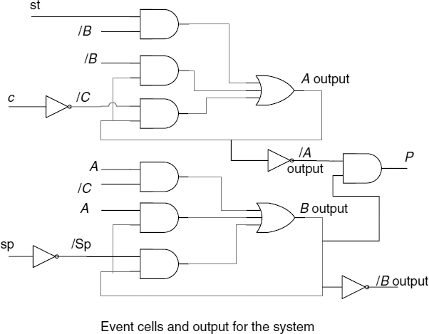
Figure 9.7 Final circuit for the system.
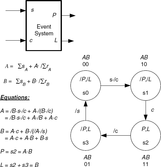
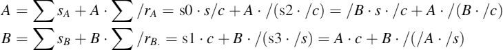
Figure 9.8 Event-driven single-pulse system with memory showing block diagram, state diagram and equations.
Therefore, when the FSM moves from state s0 to s1 it waits in s1 for the c input to go to logic 1, then moves to state s2 where P and L are made logic 1. This will happen on the 0 to 1 transition of the c input. The FSM will remain in state s2 until the c input again drops to logic 0, and the FSM will move to state s3 where the output P will resume its logic 0 state while the output L remains at logic 1.
At this point, the FSM will remain in state s3 until the input s reverts back to logic 0, ready for the next single-pulse generation. This will also cancel the output L. In this design, the output L is being used as a pulse indicator, since the pulse duration is dependant upon the width of the c pulse and may not be seen by the user.
In this system, the actual width of the P output pulse can be controlled by the logic 1 period of the c input.
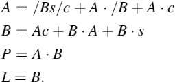
Turning to the equations, the two-event cell equations can be obtained in the same way as in the previous example, by first obtaining the turn-on set and then the turn-off set for each equation, then inserting them into the sequential equations. However, a little thought shows that each sequential equation can be written down directly using the short-cut method, more or less as has been done in Figure 9.8:
with outputs
P = s2 = A · B
and
L = s2 + s3 = A · B + /A · B = B.
The two-event cell equations can now be converted so that they can be implemented with sum of product logic (typically found in PLD devices):
The circuit is illustrated in Figure 9.9. Notice the Reset line (thick line) to initialize the event cells to zero. This is essential in order to ensure that the system is reset to state s0. In operation, this Reset line will be at logic 1. During reset it will be at logic 0, thus clearing both event cells to zero. Clearly, the reset line is ANDed with the turn-on/turn-off logic of the event cells:
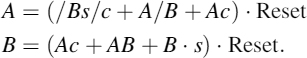
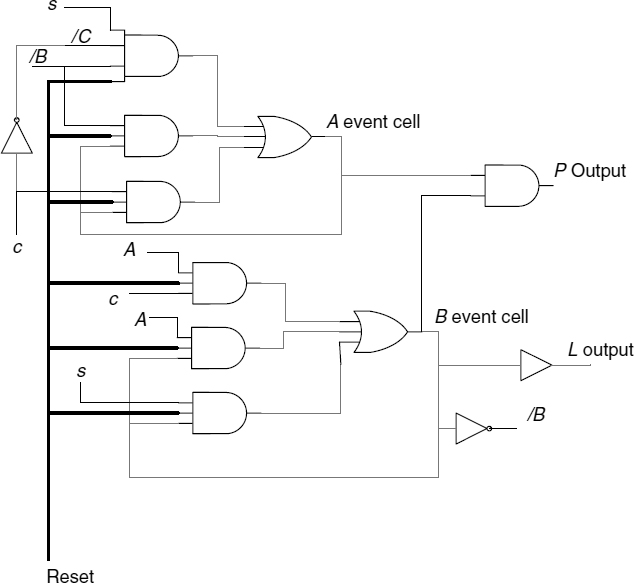
Figure 9.9 Circuit for the event-driven FSM system.
For clarity, the Reset input line will be left out of the event cell equations, but remember to add it in when implementing each design, otherwise the circuit will not simulate, since it will not be able to initialize. At this stage the reader might like to revisit Figure 9.7 and add a reset connection to allow this circuit to reset to state s0.
9.6 ANOTHER EVENT FINITE-STATE MACHINE DESIGN FROM SPECIFICATION THROUGH TO SIMULATION
In this next example, an event FSM will be developed from its written specification through to a Verilog HDL description of the FSM (as described in Chapter 6). This is then simulated using the Syncad™ simulator system.
The idea here is to illustrate how a complete design can be implemented. Later, the Verilog file could be used to program a PLD device and, hence, realize the design in physical hardware.
9.6.1 Important Note!
Since the Verilog behavioural level is not optimized for an event-driven system, as yet, the Verilog description is at the Boolean equation level. This is fine for our purposes, since it will provide a one-to-one correspondence with the system equations. It is also possible to implement the event-driven system using the gate level direct. The Boolean equation level, however, is useful for quick simulation and verification. On the other hand, simulating in terms of the logic gates allows the designer to experiment with different gate delay values to ensure that the circuits will not maloperate due to violation of the 33.3% gate tolerance rule (see Section 9.12.3 and Reference [1] for details).
9.6.2 A Motor Controller with Fault Current Monitoring
This is an event-based FSM used to control a motor. An external device (possibly based on a Hall-effect transducer) is used to monitor the motor current. This will be set so that normal start current is allowed, but if the motor current exceeds some defined limit a fault signal will be sent to the FSM to switch off the motor and light up a fault LED indicator. The details of the Hall-effect fault circuitry and the power circuit to switch the motor on and off are excluded from the diagram of Figure 9.10a.
Figure 9.10b shows the state diagram for the FSM controller. The motor can be switched on by asserting input st, and off by disasserting input st. If a fault is encountered by the Fault Detection Unit its output signal ms will go high thus causing the FSM to move into state s2 where the motor will be switched off and the Fault indicator L turned on (an active-low signal). The system will remain in s2 until the start input st is disasserted to move the FSM into state s3 turning off the Fault indicator LED L. The FSM can return to its initial state s0 on reaching state s3 if input t is logic 0.
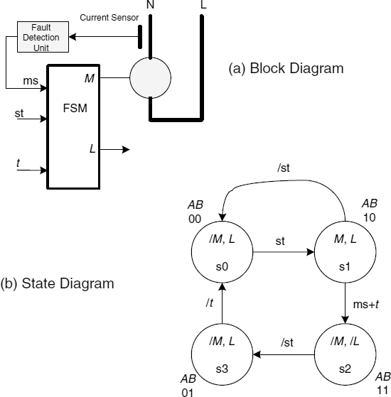
Figure 9.10 The block diagram and state diagram for the motor controller.
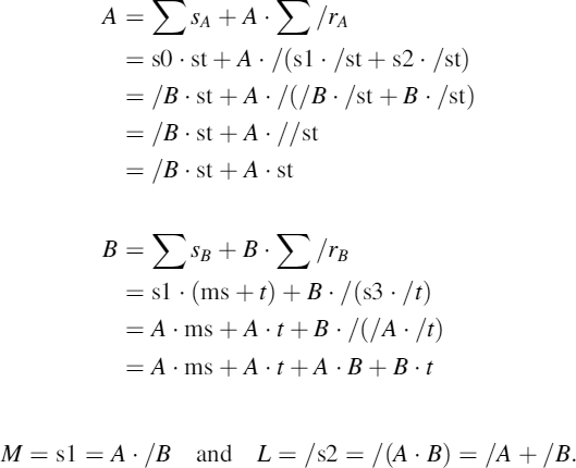
The system can be tested in the absence of a fault by pressing the test input t. Note that t = 1 will hold the FSM in state s3. The equations for the event cells can now be developed:
The schematic diagram of the design is illustrated in Figure 9.11. This has the test input included so that the system can be tested in the absence of a fault input.
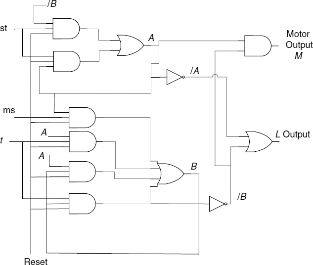
Figure 9.11 Schematic circuit diagram for the FSM controller.
Although it is not necessary to draw a circuit diagram, it is useful to see the circuit of the FSM. Note that the essential interface buffering between the low-voltage FSM circuit and the high-voltage motor circuit is not shown.
This design can be developed as a Verilog module and this is illustrated in Listing 9.1.
///////////////////////////////////////
module fsm(rst,st,ms,t,M,L,A,B);
   output M,L,A,B;
   input rst,st,sp,ms,t;

assign
   A = (~B&st | A&st)&rst,
   B = (A&ms | A&t | A&B | B.t)&rst,
   M = A&~B,
   L = ~A | ~B;
endmodule
////////////////////////////////////////
Note that the module inputs and outputs are defined outside of the parentheses, as was usual in older style Verilog modules. This is still supported in later versions of the Verolog compiler tools. Chapter 6 shows the more recent way to define the inputs and outputs.
In the Verilog file, the event equations have been implemented using an assign with blocking statements. The equations also cater for the test t input to test the system in the absence of a fault.
The Verilog code in Listing 9.2 is a test bench that is used to test the design. A test bench provides an instance of the FSM, along with a set of test signals to be used in the simulation in order to verify the design.
module test;
reg st,ms,t,rst;

fsm uut(rst,st,ms,t,M,L,A,B);

initial
    begin
    $dumpfile (“motflt.vcd”) ; // to get a printout of waveforms.
    $dumpvars;
    rst=0;
    st=0;

    ms=0;
    t=0;
// Note it is important to ensure signals change in
// proper sequence. Also to ensure ms and sp are
// mutually exclusive.
//---------------- remove reset
    #20 rst=1;
//---------------- move to s1
    #20 st=1;
//---------------- stay in s1
//---------------- move to s0
    #20 st=0;
//---------------- move to s1 again
    #20 st=1;
//---------------- move to s2
    #20 ms=1;
//----------------
    #30 ms=0;
//---------------- move to s3
    #20 st=0;
//---------------- move back to s0
    #20 st=0;
//---------------- move to s1
    #20 st=1;
//---------------- stay in s1
//---------------- move to s2
    #20 t=1;
//---------------- move to s3
    #20 st=0;
//---------------- move to s0
//---------------- end of tests.

$stop(60); // stop the simulation.
    end
endmodule
Listing 9.2 Test-bench module.
The FSM module is very simple and, apart from the input and output defines, consists of only an assign block. The event cells are defined individually within this block, together with the output equations.
The test bench module is also seen to be quite simple. One point to note is that the signals must change one at a time, and with a time delay. This is mandatory, since the event cells can respond to potential static 1 or 0 hazards (glitches). This will be a necessary requirement with all event-driven designs.
Finally, Figure 9.12 illustrates the timing waveforms from the simulation.
Comparing this with the test bench module sequence, it can be seen that the state diagram has been traversed twice: once with a fault signal and next with a test signal.
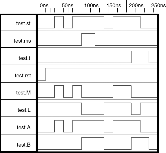
Figure 9.12 Verilog simulation of the design.
Note that, in the case of a fault, the transition from s2 to s3 to s0 is very fast and the s3 state is not apparent in the simulation. In the case of the test, the FSM stops in state s3 until the t input is returned to its low state. In this way, the operator can test the complete state sequence (particularly if the state variables are available as LED indicator outputs).
9.7 THE HOVER MOWER FINITE-STATE MACHINE
A hover-type lawnmower usually uses a mechanical interlock to prevent the motor from starting unless the user presses a button before operating the on/off lever. By replacing the mechanical mechanism with an electronic equivalent, the safety mechanism can be made easier to manufacture.
9.7.1 The Specification and a Possible Solution
A hover lawnmower has a safety button sf that must be pressed before operating the start lever st. When the safety button is pressed, an LED indicator P is lit; when the start lever st is operated after this, the motor will turn on. The motor can be stopped by releasing the start lever. The safety button sf must be pressed before the motor can be restarted with the start lever.
A block diagram with a suitable state diagram for the system are illustrated in Figure 9.13a and b. The specification is a typical one that might be given as a specification for a product. Looking at the original state diagram 1 in Figure 9.13b (with four states), it can be seen that a number of safety features have been added. This was done during the development of the state diagram as the true nature of the control sequence was revealed.
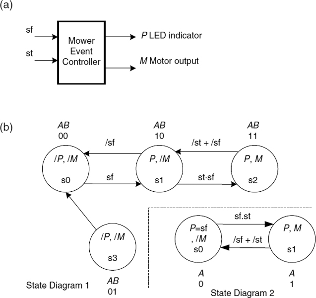
Figure 9.13 (a) Block diagram of the mower FSM controller. (b) Two possible state-diagram solutions.
The state diagram controls the sequence of the controller by ensuring that only if the safety button is pressed before the start lever is operated will the motor operate. The P LED will remain on in s1 if the start button is released. If the safety button is released in either states s1 or s2 the FSM will move back to state s0.
Note that the FSM will return to s1 when the start lever st is released or the safety button is released. This ensures that the operator's hands are on both the safety button and the start lever in order to start the motor. The operator must see the LED P turn on before the start lever can be used to turn on the motor. Finally, note that the unused state s3 has been returned to s0. This ensures that the system will fall into s0 should a glitch cause it to get into this unused state.
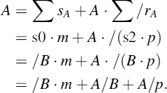
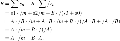
Returning to Figure 9.13, state diagram 2 (with only two states) is an alternative solution, where combinational logic is used on the inputs (along the transitional lines between s0 and s1). The logic equations can be deduced in the usual way:
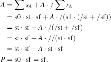
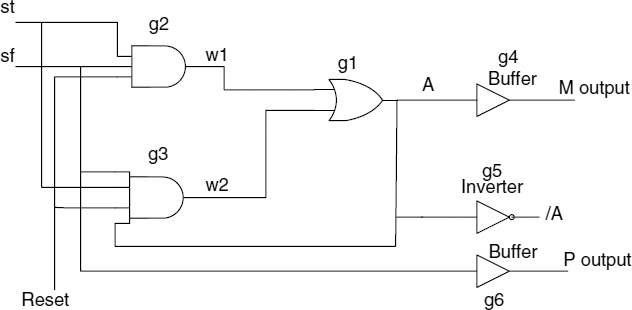
Figure 9.14 Schematic circuit diagram of the mower FSM.
This latter equation can be seen by noting that the P indicator can be on in s0 (Mealy output) and also in s1 as a result of getting into s1 via inputs sf · st.
M = s1 = A.
This leads to more simplified logic requiring only three logic gates: two AND gates and one OR gate. Buffers would, of course, be required for outputs P and M.
Figure 9.14 illustrates the circuit for the mower FSM of state diagram 2 in Figure 9.13. Additional buffers have been added to provide appropriate power levels. In particular, the motor output M would need to be connected to a relay (static or electromechanical) to isolate the FSM from the mains electrical supply.
The FSM of state diagram 2 is implemented in Verilog using a gate-level module. This allows individual gates to be given propagation delay values. This is shown in Listing 9.3.
module mowerfsm (st,sf,P,M,A, rst);

    input st,sf,rst;
    output P,M,A;
    wire na,nb,w1,w2;

    or #5 g1(A,w1,w2);
    and #5 g2(w1,sf,st,rst);
    and #5 g3(w2,A,st,sf,rst);
    //----------------
    buf #5 g4(M,A);
    //----------------
    not #5 g5(na,A);
    buf #5 g6(P,sf);
    //----------------

endmodule
The test bench module is illustrated in Listing 9.4.
module test;
    reg rst, st, sf;
    mowerfsm uut(st,sf,P,M,A,rst);

    initial
      begin
         $dumpfile (“mower.vcd”);
         $dumpvars;
         rst=0;
         st=0;
         sf =0;
         #20 rst=1;
         #20 sf =1;
         #20
         #20 st=1;
         #20
         #20 st=0;
         #20
         #20 st=1;
         #20
         #20 sf=0;
         #20
         #20 st=1;
         #20
         #20 st=0;
         #10 $finish;
end

endmodule
Listing 9.4 Test-bench module.
Figure 9.15 illustrates the simulation of state diagram 2 in Figure 9.13. This follows the test-bench sequence of Listing 9.4.
The simulation starts by activating the sf input. The P indicator turns on. This is followed by the st input going high, which starts the mower motor. The start input is released and the motor stops. It can be started again with the start input because the sf input is still activated. The sf input is then deactivated (with the start input st still asserted) and the motor turns off.
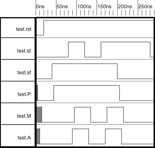
Figure 9.15 Mower FSM simulation.
Returning to the problem again, and after a little thought, the control of the mower can be reduced to a combinational one requiring
This final solution is now obvious when seen, and perhaps you saw this at the beginning of this example. This is effectively back to a mechanical switch design!
The original solution based on state diagram 1 in Figure 9.13 is correct but requires three states and two event cells. The second attempt provides an equally working solution with fewer states using state diagram 2 in Figure 9.13. Finally, the combinational solution provides the simplest solution. It pays to look at the problems carefully to see whether they can be simplified. The sequential nature of the specification can easily lead to this kind of overdesign from the designer.
9.8 AN EXAMPLE WITH A TRANSITION WITHOUT ANY INPUT
Now consider the next example in Figure 9.16; in this example, the transition between s3 and s0 does not have any input.
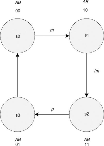
Figure 9.16 State diagram with no input along a transition.
Here are the equations for this example:
The equation for B will be obtained by not using the short-cut rule:
In the equation for B, the ∑/rA term is (by the short-cut method) // s3 which is //A because there is no input term along the transitional line.
This example does not have any output (something that most FSMs would have), but it is only an academic example.
Remember: add the reset input before trying to simulate the design.
9.9 UNUSUAL EXAMPLE: RESPONDING TO A MICROPROCESSOR-ADDRESSED LOCATION
Now here is an unusual example. Suppose one has an FSM-based event controller chip (PLD/FPGA) that is required to synchronize with a microprocessor. A possible solution follows.
In the system shown in Figure 9.17, an address 380h is produced by the address decoding logic. This might be implemented on the PLD/FPGA chip. The output of this is the signal 380h, which is to be used to operate the FSM.
The FSM will respond to this signal when c is low by moving to its state s1, where it will wait for c to go high.
At this point the FSM will move to s2 to assert the ACK signal to signal to the microcontroller that it has seen the 380h signal. The FSM will return to its initial state when the signal c goes low again via state s2 and s3. The signal c is derived from the system clock.
Note that this signal is used by the event FSM to control the return to initial state and thus provide a clearly defined ACK pulse width. If this were not done, the width of ACK signal would be dictated by the propagation time of the event logic only.
The state diagram is shown in Figure 9.18. Here, one can see the turn-on and turn-off terms, derived from the address decoder and c clock signals. This example shows how a simple event-driven FSM can be used to provide a control action without having to add a lot of logic to the system.
In a microprocessor system, the address decoding logic might well be already available; in a microcontroller system the FPGA could provide the decoding logic as well as the FSM, although it is using up a lot of I/O pins. The ACK signal, as implied in Figure 9.17, could be used to cause an interrupt in the microprocessor system, thus avoiding the need to provide an input port bit.
Figure 9.17 Block diagram of the basic address-activated system.
Figure 9.18 State diagram and equations for address-activated FSM.
This system will work correctly if the clock signal c connection between the microprocessor and the FSM is short to avoid lead delays. It is also assumed that the clock period is much greater than the largest propagation delay in the FSM, so as to allow the FSM time to settle.
The equations are
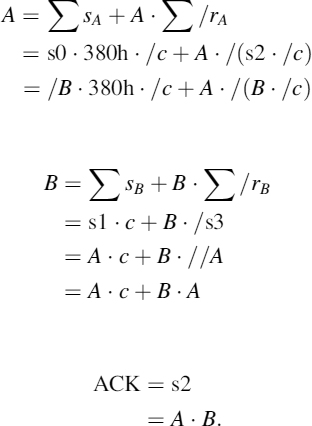
9.10 AN EXAMPLE THAT USES A MEALY OUTPUT
Sometimes it is useful to have an output that is a function of one or more inputs, but only in particular states. You might remember that during the programmed learning sections a Mealy FSM was defined as one in which some of the outside world inputs were fed into the outside world decoder. This next example illustrates this.
9.10.1 Tank Water Level Control System with Solutions
In the example shown in Figure 9.19, a pump is used to fill the tank (by making P1 = 1 and P2 = 0). The idea is to fill the tank so that the liquid level is between the level sensors Sh and Sl. When this is the case, the outlet flow from the tank is balanced by the inlet flow to the tank via the pump.
If the liquid level falls below level sensor Sl (l1 asserted), the pump is to be switched to highspeed mode where P1 = 0 and P2 = 1. This is important to avoid air locks in the outlet part of the system.
Should the liquid level rise to level Sh (l2 asserted), the pump is to switch off.
This system will work continuously to maintain the liquid level. It can, of course, be switched on, or off via the relevant switches st and sp, which could be replaced with a single on/off switch if desired.
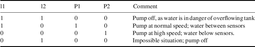
Table 9.3 shows the relationship between the level sensor inputs l1 and l2, and the outputs to the pump P1 and P2 can be constructed as illustrated below. Note that the last row of Table 9.3 is dictated by the practical arrangement of the system. Clearly, the water level cannot be at the high setting in the tank and there be no water at the lower setting.
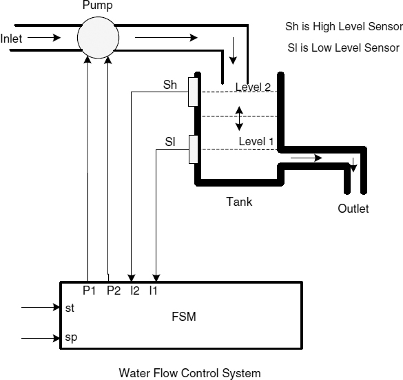
Figure 9.19 Block diagram of the FSM-based Mealy pump control system.
Table 9.3 Relationship between level sensor inputs and outputs to the pump.
From this information, a state diagram can be developed that will meet the required specification. Figure 9.20 illustrates the state diagram. In this design, the system resets in to its idle state and waits for a start signal. Once obtained, the system moves into s1, the dormant state. It will stay in this state while the water level is above the level 1 sensor. The level sensors will now dictate when the system will move to s3. This will only occur if sensor l1 is zero, so the P2 input can start the pump in high mode to pump water above the lower level sensor. Once in state s3 the FSM will move between s3 and s2 to maintain the water level between the two level sensors.
Note that the system can be stopped at any time and the FSM will fall back to state s0. Note also that the P2 output will be disabled in state s3 if stop is activated, thus preventing the pump speed changing on a transition from s2 to s3 to s1 to s0. The water level would then fall to empty once the system was turned off. If the tank is empty when the system is turned on, then the FSM will move from s0 to s1, then straight to s3 to fill the tank to a level between l1 and l2.
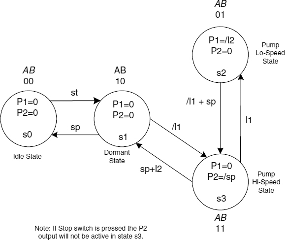
Figure 9.20 First attempt at a solution: four-state FSM with Mealy output.
This solution can now be developed into a practical system by assigning a set of secondary state variables. In this example, possible assignments could be
![]()
or perhaps
![]()
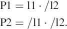
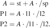
Looking at this solution, one may wonder if it could be made simpler. In fact, looking at the table of sensor inputs and pump outputs, there is a combinational equation that can be formed using the level sensor inputs l1 and l2, and the two pump outputs P1 and P2. This is because the physical liquid movement forms a natural sequence for the problem. Lookback to Table 9.3 with the impossible situation of l1 not active but l2 active, in which the pump should be held off. The equations for P1 and P2 are
However, these on their own are not enough, since there is the start and stop switch inputs to consider. Assuming that these two switches are push buttons, an event memory cell is needed to allow the system to occupy the two states.
The final system is illustrated in Figure 9.21. Here, the system is only able to operate when it is in state s1. In state s0 it is disabled.
The two equations for P1 and P2 are only true when the FSM is in state s1. Therefore, the two equations are written in the form
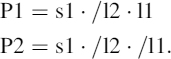
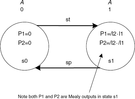
Figure 9.21 Final solution: two-state FSM with Mealy outputs.
To obtain the event cell (there is only one in this state diagram)
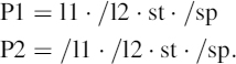
A = ∑sA + A · ∑/rA.
Therefore:
A = s0 · st + A · /(s1 · sp).
Replacing s0 and s1 with the secondary state variables gives
A = /A · st + A · /(A · sp)
The /A in /A · st and the A in A · sp need to be dropped (short-cut method), leaving
A = st + A · /sp.
This is because when the /A term in /A · st is dropped the result is effectively 1 · st, since /A · 1 = /A.
In a similar way, A · sp is 1 · A · sp which is 1 · sp = sp. Therefore, the final set of equations for this example is
Finally, before leaving this example, it is possible to reduce this particular problem to a combinational logic circuit that does not require an event cell. This is possible owing to the physical nature of the problem. The water in the tank creates a sequential operation for the water level sensors.
This is only possible if the design uses switches that remain open or closed when released. If the system uses push switches that release when one leaves go of them, then the event cell is needed to remember the switch action.
9.11 AN EXAMPLE USING A RELAY CIRCUIT
The event sequential equations can be used to implement a design using relay logic. This might seem to be an outdated way to implement an FSM, but, in some cases, old-style electromechanical relays might be a more preferred solution. Alternatively, semiconductor static relays could be used in place of electromechanical relays. Both could be designed to operate at high voltage or high current levels.
In this next example, the design will be implement using logic gates and then relay logic.
Consider the following specification, which is very similar to the motor controller problem of Section 9.6.
A motor can be started by pressing the start button st, provided the stop button sp is not pressed. It can be stopped by pressing the stop button provided the start button is not pressed. If the stop button is pressed while the start button is still pressed, then the motor is to stop and an indicating LED turned on. The system can only leave this state and return to its initial state via a manual reset-key-activated switch. The reset key switch can also be used to deactivate the system regardless of the state of the start and stop buttons.
The state diagram in Figure 9.22 is developed to implement the specification. In this state diagram, the motor can be started by pressing the start button st thus moving the FSM to state s1, but only if sp = 0. The motor can be stopped by pressing the stop button to move the FSM back to state s0, provided st = 0. Pressing the stop button while the start button is still pressed will cause the FSM to move to s2, which is an invariant state (from which the FSM cannot leave without a system reset). The idea is to allow the reset input to move the FSM back to state s0.
From this, a set of equations can be derived, resulting in
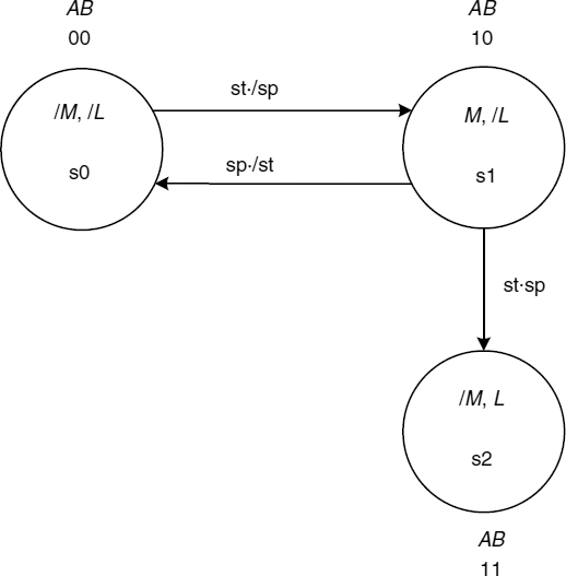
Figure 9.22 Motor controller state diagram.
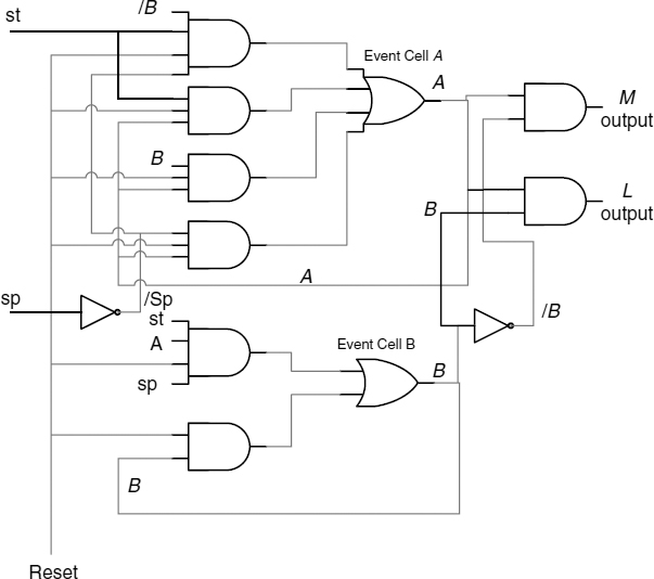
Figure 9.23 Logic circuit for the motor controller FSM.
Note, there is no turn-off term in the B equation, so the negated term is /0, which of course is 1. The outputs are:
M = s1 = A/B
L = s2 = AB.
These equations are in a suitable form for implementing the design using either a PLD or relays.
A circuit schematic is drawn in Figure 9.23. This circuit uses AND/OR/NOT logic, so is suitable to be implemented using a PLD device. Note that an AND gate is needed in the feedback loop for event cell B so that the reset can be used to reset the cell back to its zero state.
However, a little thought will reveal that such a circuit needs a 5 V power supply, and this would need to be obtained from the mains supply via a transformer and rectifier circuit. The transformer could be replaced with a mains resistor dropper and single diode and capacitor, but this still requires these overheads.
An alternative design could be based upon electromechanical or static relays. These have the advantage that they can be used with a very rough power supply direct from the mains (using relays that can be operated at mains voltage of course). The relay circuit is obtained directly from the sequential equations.
The circuit in Figure 9.24 is the final result. In this diagram, the relay contacts are shown with the relays not operated. This circuit will use a simple half-wave rectifier in series with a suitable capacitor to obtain a rough DC voltage for the relays A and B. The resistor across the capacitor provides a discharge path when the supply is disconnected (by a reset for example).
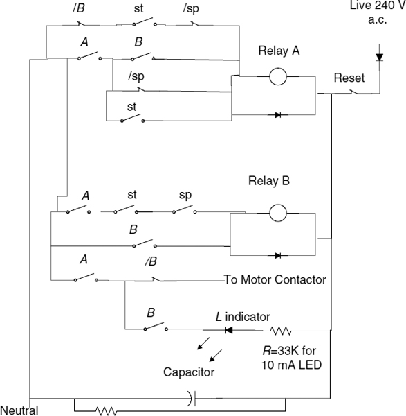
Figure 9.24 Relay logic for the motor controller FSM.
The circles A and B represent the relay operating coils (or control input to static relays). The diodes across each coil are needed to provide a path for relay current when the contacts open; otherwise, the large EMF across the coils could damage the switch and relay contacts. These are usually referred to as ‘catching diodes’.
Note: the reset switch is in series with the supply. This can reset both relays and turn off both the motor and indicator LED.
Before moving on to look at more asynchronous (event-driven) examples, one needs to consider the effects of race hazards in event-driven types of FSM.
9.12 RACE CONDITIONS IN AN EVENT FINITE-STATE MACHINE
In this section some of the problems that can occur in asynchronous (event) FSM systems will be discussed, with suggestions on how they can be eliminated.
In an event FSM there are three types of potential race condition:
- race between primary inputs;
- race between secondary state variables (the event cells themselves);
- race between primary and secondary variables.
This is particularly important, since one needs to be aware of potential problems that can occur in event-driven systems in order to avoid making design errors. These are used with permission from Oxford University Press from their publication Problems and Solutions in Logic Design [1].
9.12.1 Race between Primary Inputs
This is when two signals both happening at the same time on the same transition of a three-way branch state are expected to cause the FSM to move to one particular state. Clearly, one cannot guarantee that two (or more) input signals will change at the same time, since there are always delays in the paths from two or more signals.
Note: to avoid this type of condition, do not try to look for more than one input changing at the same time.
In the example of Figure 9.18 there are two signals 380h · /c along a transitional line, but in this case the FSM was looking for the condition 380h AND /c, and in the next state c was to be seen to go high before a state change (it must have been low to get to this state). So, this is a very different situation, where the inputs have a dictated sequence and cannot cause confusion if they happen at the same time.
9.12.2 Race between Secondary State Variables
This is when the designer has not followed a unit distance coding for the secondary state sequence (A, B, event cells for example). The use of a none unit distance coding can result in the FSM falling into a state different to the one intended as a result of unequal propagation delays between event cells.
Consider the earlier state diagram of Figure 9.18 with the following secondary state assignment:
![]()
If, in state s0, the 380h input is 1 and c is 0, with A changing to 1 before B, then the resulting transition might be s0 to s2, and in s2, since c is still logic 0, a further transition to s3. Since there is no input along the transitional line between s3 and s0, the FSM would move back to s0! This sort of behaviour is unpredictable, since if it was B that changed first in state s0 then the transitional path could be s0 to s3, back to s0.
Remember, in an asynchronous (event-driven) FSM there is no synchronizing clock to introduce a delay to allow signals to settle.
Solution: always use a unit distance code for asynchronous (event) FSM systems.
9.12.3 Race between Primary and Secondary Variables
The final race condition to look at is also the most complex. There are more details to be found in Reference [1].
Essentially, as the heading suggests, this is a race between the primary (outside world) inputs to the FSM and its event cell operation (secondary state variables). This is caused if the propagation delay through to the primary input path to set the cell is greater than the secondary delay path (cell output to cell input to cause the cell to set or clear). It can result in the cell maloperating.
To prevent this kind of race from occurring, ensure that the primary delay Tp is less than the secondary delay Ts at all times, i.e.
Tp < Ts.
More specifically:
Tpmax < Tsmin.
This leads to the identity defined in Reference [1], repeated here by permission of Oxford University Press:
Tpmax/Tsmin < 1,
where Tpmax is the maximum possible propagation delay for a primary input path and Tsmin is the minimum possible delay for a secondary delay path (total gate delays between A and B outputs, for example).
The event cell structure used in the asynchronous designs in this book (and, indeed, in the Zissos book [1]) meet these requirements if the gate tolerances are within 33.3% of each other. This is not difficult to achieve in modern integrated circuits, particularly PLD and FPGA devices.
There is also a somewhat dated paper on gate tolerances in Reference [2] that is worth studying.
9.13 WAIT-STATE GENERATOR FOR A MICROPROCESSOR SYSTEM
Some microprocessor systems have a feature that allows the processor to introduce ‘wait states’ into a particular memory cycle.
Figure 9.25 shows the basic input or output (I/O) cycle timing (simplified for this example, but accurate in its sequence to produce a working design). In this example, it is assumed that each memory or I/O cycle consists of four T states created by the system clock c. T1 is address setup time, T2 read or write setup time, T3 a wait state to allow the data bus time to settle, and T4 used to read or write data. In this figure, the event FSM controller monitors the chip enable signal ce, which will go low when a slow I/O device is selected by the microprocessor software. This will occur in the T1 timing slot for the particular I/O cycle. There are four T slots per I/O access. During the T2 period of the clock, either the input/output write w or the input/output read r signal lines will be taken low by the microprocessor.
During the T2 period, an output signal from the FSM (IORDY), which is a special input signal to the microprocessor, can be taken low, and if the microprocessor detects this during the T2 period it will insert an additional T period Tw between T3 and T4.
This extra period is known as a wait state (Tw) and it effectively increases the T3 period used to allow slow devices time to settle before the T4 period that is used to perform the data transfer. In this way, a slow I/O device can have its chip enable ce signal monitored by the FSM controller and used to generate a wait state. To be sure, the particular microprocessor will need to be consulted to find out how to activate a wait state, but this is usually available in the data sheets for the microprocessor.
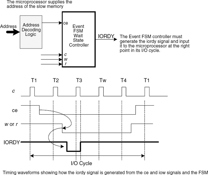
Figure 9.25 Showing the block diagram and memory/IO cycle timing.
The purpose of the event FSM controller is to identify when to send the IORDY signal line low, and when to return it high again. In effect the event FSM is being used to detect the point in the timing diagram of Figure 9.25 at which to generate the IORDY signal to be sent to the microprocessor.
Using the timing diagram as a guide, the required state diagram can be developed as seen in Figure 9.26. As can be seen from Figure 9.26, the state diagram follows the sequence by detecting ce and either w or r going low in state s0 to turn on the IORDY (active-low) signal in T2. Then, it detects when the clock c goes low in state s1 in order to identify when it goes high in state s2 (to identify entry into T3 state). The FSM must then determine when the clock signal c goes low again, indicating the point at which IORDY must go high again.
Note that fast memory cycles will not activate the wait-state generator because those chip select signals will not be connected into the wait-state event FSM controller.
Finally, Figure 9.27 illustrates the sequential equations and output equation for the system. This example has illustrated how an event-driven FSM can be used to track points in a sequential sequence of signals. This example could easily be adapted for a particular microprocessor. However, one must determine the correct sequence from the microprocessor data sheet, since different microprocessors use their own signals and sequences to control access to slower memory.
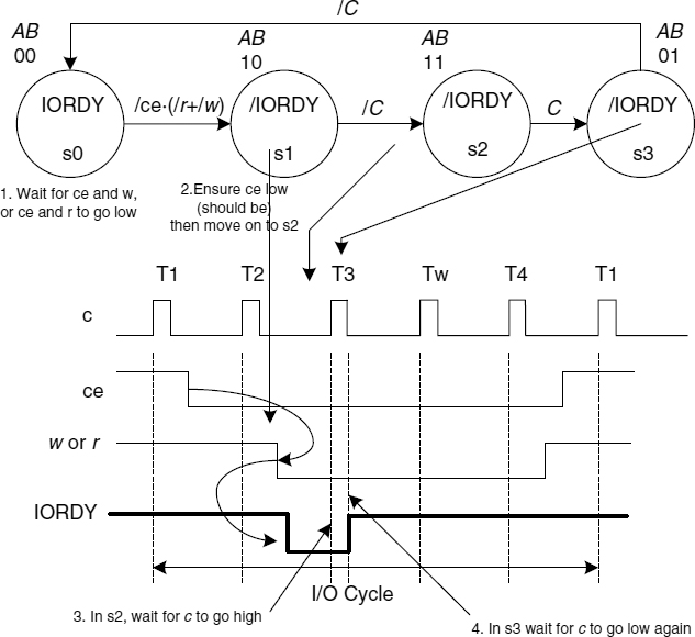
Figure 9.26 The state diagram and how it was derived from the timing waveform.
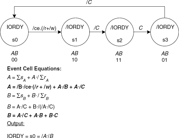
Figure 9.27 The sequential equations for the memory/IO FSM controller.
9.14 DEVELOPMENT OF AN ASYNCHRONOUS FINITE-STATE MACHINE FOR A CLOTHES SPINNER SYSTEM
Figure 9.28 illustrates the system. There is a spin motor to spin the clothes drum at high speed so as to remove excess water from the clothes by centrifugal force. The water released from the clothes into the drum is removed by the pump. There is a water level sensor to detect whether the water level is too high before turning on the spin motor to avoid excess load on the latter.
The user loads wet clothes into the clothes drum and presses the start button st. This starts the pump on release of the start button. When the water level is below the water level sensor, the spin motor is started and a timer (not shown here) is started.
In due course, the timer times out and the system stops both the spin motor and the pump. A done indicator is illuminated to indicate to the user that the spin cycle is complete. The user must press the stop button sp before another spin cycle can commence. This system does not have a sensor to test that the door is closed. You might like to add this to the system and modify the state diagram to include this feature.
A suitable state diagram is illustrated in Figure 9.29. In this state diagram, on pressing the start button a test is made to determine whether the water level is above or below the sensor on the drum. If above the sensor, the FSM moves to s2 via s1 and starts the pump.
Note, the pump can only start if the start button has been released. Once the water level has dropped below the sensor, the FSM moves to s3 to turn on the spin motor, as well as start the timer. At time out, the FSM moves to s4 to turn off both spin motor and pump as well as turn on the done indicator D. Note that the FSM cannot leave s4 via any transition. In fact, the stop input acts as a reset input and can stop the system in any state.
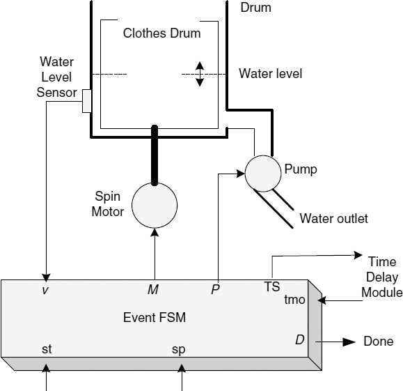
Figure 9.28 Basic system showing a clothes spin system with FSM.
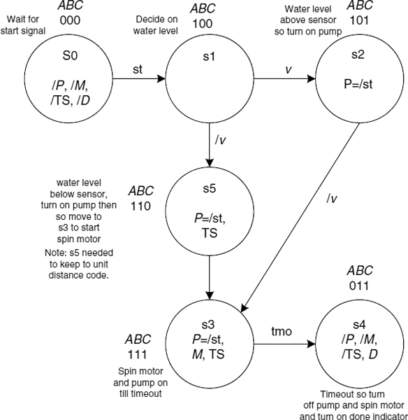
Figure 9.29 State diagram of a possible solution for clothes spinning system.
If, on starting the system, the water level in the drum is below the water level sensor, the FSM will move from s0 to s1, to s5, then directly to s3. State s5 is needed to allow a unit distance code to be used for the state machine; s5 is in fact a dummy state.
Note that there is no input along the transitional line connecting s5 to s3. This implies that when the FSM moves into s5, it will immediately move on to state s3, the delay being that of the propagation delay of the logic used to implement the event cells B then C.
The equations for the design are
The stop input sp will be logically ANDed to each equation A, B, and C to allow the FSM to return to ABC = 000 when sp is made logic 0.
The Verilog module follows in Listing 9.5. In this module, the equation level is seen commented out and replaced with a gate-level description.
///////////////////////////////////////////////////
         // Spin motor and pump Asyhchronous FSM //
///////////////////////////////////////////////////
module smpfsm(st, sp, v, tmo, P, M, TS, D, A, B, C);

   input st, sp, v, tmo;
   output P, M, TS, D, A, B, C;
wire w1, w2, w3, w4, w5, w6, w7, w8, w9;
// equation level description. Used in Figure 9.31.
//assign
  //A = (~B&~C&st | A&~B | A&~C | A&~tmo)&sp,
  //B = (A&~v | B)&sp,
  //C = (A&v | A&B | C)&sp,

    // alternative gate level description Used in Figure 9.32.
    // each gate has been given a delay of 5 time units.

      or #5 g1(A, w1, w2, w3, w4);
      and #5 g2(w1, ~B, ~C, st, sp);
      and #5 g3(w2, ~B, A, sp);
      and #5 g4(w3, ~c, A, sp);
      and #5 g5(w4, ~tmo, A, sp);
      //-------------------------
      or #5 g6(B, w5, w8);
      and #5 g7(w5, A, ~v, sp);
      and #5 g11(w8, B, sp);
      //-------------------------
      or #5 g8(C, w6, w7, w9);
      and #5 g9(w6, A, v, sp);
      and #5 g10(w7, A, B, sp);
      and #5 g12(w9, C, sp);
      //-------------------------
P = A&C&~st | A&B&~st,
M = A&B&C,
TS = A&B,
D = ~A&B&C;

endmodule
////////////////////////////////////////////////
Listing 9.5 Verilog module for clothes spin FSM.
The test bench module is illustrated in Listing 9.6.
‘timescale 1ns / 10ps
module test;
    reg st, sp, tmo, v;
    smpfsm uut(st, sp, v, tmo, P, M, TS, D, A, B, C);
    initial
      begin
         sp=0;
         st=0;
         v=0;
         tmo=0;
         ///////
         #10 sp=1; // remove reset.
         #10
         #10 v=1; // water in drum.
         #10
         #10 st=1; //start system
         #10 //should move to s1 then s2.
         #10 st=0;
         #10 // starts pump to empty drum.
         #10 // wait for drum empty.
         #10 v=0; // signal that drum empty.
         #10 // should move to s3 and turn on spin motor
         #10
         #10 //waiting for timer to stop spn motor.
         #10 tmo=1; // signal to stop spin motor.
         #10 // should have moved to s4.
         #10 tmo=0;
         #20 st=0; //return start to off state.
         #10 sp=0; //stop system and return to s0.
         #20
         #20 sp=1; // release reset buton.
         #10 st=1; //start system with empty drum.
         #20
         #20 st=0;
         #20 // should move to s1 then s5 then s3.
         #10 tmo=1; // time out. should move to s3.
         #20 //waiting for user to press stop.
     #10 $stop;
     end
endmodule
Listing 9.6 Verilog test-bench module.
Finally, the simulation is shown in Figure 9.30 using the equation-level description. In the simulation, the event cells A, B, and C appear to be changing state at the same time in some parts of the simulation, but in fact the transitions are so fast that the actual transitions cannot be seen. However, care must be taken to ensure that propagation timing satisfies the 33.3% rule discussed in Section 9.12.3.
In Figure 9.31, the simulation using the gate-level description is seen. Here, each gate has been given a delay value of 5 time-units so that the state transitions can be clearly seen. In Figure 9.31, the delays between the gates allow the state transitions to be seen clearly. For example, the transitions between s1 (ABC = 100) and s2 (ABC = 101), and the transitions between s1 (ABC = 100) to s5 (ABC = 110), then on to s3 (ABC = 111). The dashed lines help to identify these transition points.
Figure 9.30 Simulation of a clothes spinner system using equation-level description.
Figure 9.31 Gate-level simulation of a clothes spin system.
9.15 CAUTION WHEN USING TWO-WAY BRANCHES
In the state diagram of Figure 9.10 there is a two-way branch in state s1 with /st along one transitional line and ms + t along the other. These inputs must be mutually exclusive, otherwise the FSM could maloperate. If this cannot be guaranteed, then the design will need to be changed so that the state diagram can only change from one state to the next on a single input change.
Figure 9.32 illustrates a possible alternative design (without the test input t). In this arrangement, the FSM can move from s1 to s2 if either the start input st is returned to logic 0 and/or if the fault input ms becomes logic 1. On reaching s2 from a fault, the motor is turned off and the fault indicator L turned on (active-low). If the st input is now returned to logic 0, then the fault indicator can be turned off but the FSM can only return to s0 if the fault input ms returns to its logic 0 level.
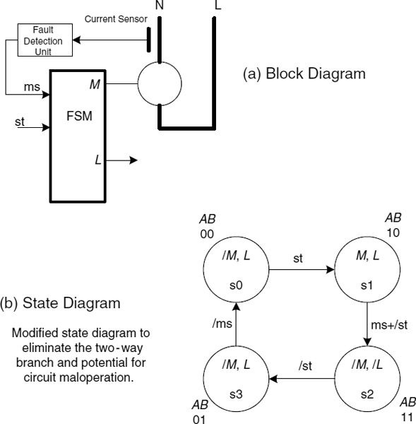
Figure 9.32 Modified state diagram for the motor controller of Section 9.6.2.
The equations for A and B are
The output equations are the same as those for Figure 9.10.
Other examples using two-way branches in this chapter are as follows.
In Section 9.10.1, Figure 9.20, there are two possible two-way branches: one in state s1 and the other in state s3. In each case there are different inputs along each transition path that could result in maloperation; therefore, this design could fail. However, the alternative design in Figure 9.21 overcomes this problem.
In Section 9.11, Figure 9.22, there is a two-way branch in state s1. If input sp is logic 1 in state s1, then the FSM can move to either s0 if st = 0, or to s2 if st = 1. If, however, inputs st and sp were to change at the same time from logic 0 to logic 1 in state s0, then it is possible that the sequence shown below could occur:
or
The latter example appears to work correctly.
In general, however, changes in two or more input signals can result in circuit maloperation due to propagation delays between input signal changes producing static or dynamic hazards. The best way to handle this situation is to allow only one input to affect the FSM. Figure 9.33 shows how this could be done.
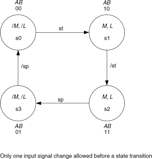
Figure 9.33 Modification to the state diagram of Figure 9.22 to avoid maloperation.
This, of course is not what the original specification for this FSM was designed to do. In fact the idea of trying to produce an event FSM to meet the specification in Figure 9.22 is not very practical.
Designing an asynchronous FSM to work correctly under multiple changing inputs is not easy and is beyond the scope of this book. Reference [3] is a good source that covers in detail and in a formal manner how to develop complex asynchronous FSMs using both Huffman and Muller circuits. In particular, the C gate is used to decouple the set terms and reset terms. This can reduce the potential for static and dynamic hazards when two or more inputs are changing.
9.16 SUMMARY
This chapter has introduced the idea of asynchronous (event-driven) FSMs and how to design them for implementation in devices such as PLD and FPGSs, as well as relay circuits. Also, the simplest method to simulate the designs has been considered, using the Verilog HDL at the equation and basic gate levels. This allows designs to be implemented directly at either the equation or logic gate level, and avoids the problems that most HDL systems can introduce at the behavioural level when implementing event-driven controllers. A number of simple FSM designs have been considered, showing how the event FSM can be used. In addition, the potential race problems associated with event-driven FSMs have been discussed, with ways to avoid these conditions from happening.
REFERENCES
1. Zissos D, Duncan FG. Problems and solutions in logic design, 2nd edn. Oxford University Press, 1979.
2. Duncan FG, Zissos D. Gate tolerance in sequential circuits. Proc. IEE 1971;118(2):317–320.
3. Myers C. Asynchronous circuit design. John Wiley & Sons, Ltd, 2001.