
Appendix C: Tutorial on the Use of Verilog HDL to Simulate a Finite-State Machine Design
C.1 INTRODUCTION
This appendix quickly describes an FSM model in Verilog code and then simulates it using SynaptiCAD's VeriLogger Extreme simulator. The code for the model, VeriLogger Extreme, and the code for most of the examples in the book are contained on the CDROM provided with the book.
A more detailed account of the Verilog HDL is provided in Chapters 6–8, where the language is developed at a slower and more defined pace.
C.2 THE SINGLE PULSE WITH MEMORY SYNCHRONOUS FINITE-STATE MACHINE DESIGN: USING VERILOG HDL TO SIMULATE
The design of a single-pulse generator with memory is outlined and then a Verilog HDL file is created. This Verilog file will use the most basic of the Verilog methods so as to keep it simple.
C.2.1 Specification
Whenever input s is asserted high, a single pulse is to be generated at the output P. Signal s must be returned low and then reasserted high again before another pulse can be generated. In addition, a memory output L is to go high to indicate that a pulse has been generated; going low again when the s input is returned to logic 0.
C.2.2 Block Diagram
Figure C.1 illustrates the block diagram of the system.
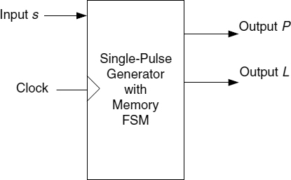
Figure C.1 Block diagram of the system.
C.2.3 State Diagram
A state diagram is implemented as illustrated in Figure C.2.
C.2.4 Equations from the State Diagram
The equations can be derived directly from the state diagram of Figure C.2, in this case using D-type flip-flops:
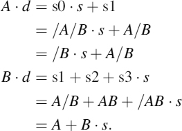
The output equations are
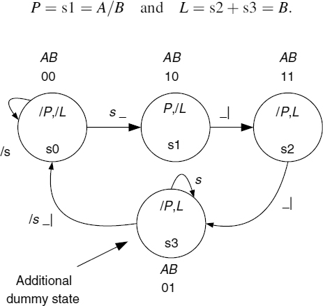
Figure C.2 State diagram of the system.
C.2.5 Translation into a Verilog Description
These equations can be translated into their Verilog form as shown below:
ad = ~B&s | A&~B,
bd = A | B&s,
P = A&~B,
L = B;
Here, the AND operator (·) is replaced with (&), the OR operator (+) replaced with (|), and the NOT operator (/) replaced with (~). Also, each equation ends with a comma (,) except for the last equation which is ended with a semicolon (;). Finally, the whole equation set must be placed into a continuous assignment thus:
assign
ad = ~B&s | A&~B,
bd = A | B&s,
P = A&~B,
L = B;
Now the Verilog HDL file will be created. To create a design using the equations just derived, a Verilog HDL file using the data-flow mode of design will be created; that is, the Verilog HDL file is developed using the predefined logic equations.
Alternative ways would be to develop the Verilog HDL file using the logic gates required to build the design or to use a behavioral structure. These alternative methods are described in Chapters 6–8.
In Verilog, a design is built up using one or more modules. A module can have one or more inputs and one or more outputs that define its terminal properties. These can, in turn, be connected together by wires.
In this example, the Verilog description is made up of three modules:
- the module that describes the behavior of the D type flip flop used in the design;
- the module that describes the FSM;
- the module that describes the tests to be carried out on the design (usually referred to as a ‘test fixture’, or ‘test bench’, or ‘test module’).
The first module consists of a behavioural description of the D-type flip-flop used in the design. Despite what has been said about the behavioural method, the D-type flip-flop is a standard circuit element that will behave as expected. This D flip-flop is created as a module called D_FF. It is illustrated in Listing C.1.
1  module D_FF(output q, input d,clk,rst);
2  reg q;
3  always @ (posedge clk or negedge rst)
4    if (rst == 0)
5      q <=1′b0;
6    else
7      q <=d;
8  endmodule
Listing C.1 The module to define the D-type flip-flop used in the design.
The behavioural description of the D-type flip-flop is a description of its terminal behavior. The key words module and endmodule define the beginning and end of the module. D_FF is its name, and the signals between the parentheses are the terminal signals of the flip-flop. In this case, q is the output and d, clk, and rst are inputs. The keywords output and input are needed to define the signal types. The line numbers are provided for reference purposes only; they are not entered when creating this Verilog code.
The flip-flop output needs to remember its last (present) state, so is further declared as a register using the keyword reg in line 2. Note that each of the lines 1, 2, 5, and 7 ends with a semicolon.
In line 3, an always keyword is used to define the conditions under which lines 4 to 7 will occur. Verilog is defining hardware, and each part of the hardware description needs to be able to execute in parallel. Thus, the always keyword with @ is used to define the conditions under which the assignments on lines 5 and 7 will occur. In this case, the conditions are either when there is a logic 0 to logic 1 transition on the clk signal (referred to as posedge), or there is a logic 1 to logic 0 transition on the rst signal (referred to as negedge).
In line 4, the conditions upon which of the two assignments on lines 5 and 7 will occur are specified using the if and else keywords. Here, if the input signal rst is logic 0, then the assignment on line 5 will occur, i.e. q <=1'b0;, otherwise the assignment in line 7 (under the else) will occur, i.e. q <=d;. Note the use of <= rather than =. This is preferred in a sequential block (see Chapter 6 for details on why this is the case).
The assignment in line 5, i.e. q <=1'b0;, assigns the logic value 0 to the output q. The 1'b0 is the way that Verilog defines a single binary bit to logic 0. Logic 1 would be 1'b1. Hence, the syntax is <number of bits> 'b< binary value, 0 or 1>.
The assignment in line 7, i.e. q <=d;, simply makes the q output equal to the input signal value of d, this being the required behaviour for the D-type flip-flop.
Finally, line 8 defines the end of the module.
Thus, it is seen that the module D_FF defines the terminal behavior of a D-type flip-flop. If the rst (reset) is taken low (negedge rst), then the if (rst == 0) will be true and the assignment of line 5 will occur q<=1'b0; to reset the flip-flop. Thereafter, if rst is taken to logic 1 (reset removed from the rst input of the flip-flop), every time the clock input clk receives a logic 0 to 1 transition (posedge clk) the q output will take on the logic value of the d input.
The behavioural methods to define logic circuits and systems are fully described in Chapters 6 and 7.
In the second module (shown in Listing C.2), called the FSM module, two instances of the D_FF are created from the D_FF module, one called FFA in line 3 and the other FFB in line 4. These are connected to the circuit of the single-pulse FSM; see signals inside the parentheses of FFA and FFB.
1  module fsm(input S,clk, output P,L,A,B);

2  wire ad, bd;
3  D_FFFFA(A,ad,clk,rst);
4  D_FFFFB(B,bd,clk,rst);

5  assign
6  ad = ~B&s | A&~B | A&~s,
7  bd = A | B&s,
8  P = A&~B,
9  L = B;
10 endmodule
Note that the terminal signals for the FSM are declared between the parentheses in line 1; they are also defined as inputs and outputs. Note also that the flip-flop outputs A and B are defined here as well. Each instance of the D flip-flop needs to be connected to external gates defined in the assignment block so they need to be defined for each flip flop instance.
In line 2, the signals ad and bd (the d inputs to each flip-flop) are defined as wires, since they are internal to the FSM module. Lines 3 and 4 define instances of the two flip-flops, using the D_FF name, followed by an instance name (FFA for flip-flop A and FFB for flip-flop B).
Note here that the A output is placed first in the parameter list since it is a q output from the flip-flop, the data d input is the ad, the clock input clk, and finally the reset input rst. Flip-flop B follows in the same manner.
So, by defining the signals used by the D_FF as q, d, clk, and rst in the behavioral description of the D flip-flop, these signals can then be connected up to the signals A, ad, clk and rst of the FFA, and B, bd, clk and rst of the FFB used in the FSM. The order of these signals is important.
The logic equations follow in lines 6–9; note that this continuous assignment begins with a Verilog keyword assign, which is needed so that the Verilog compiler can distinguish the following logic equations.
Each line ends with a comma, except the last line 9, which should end with a semicolon, thus defining the end of the continuous assignment. The assignments make use of the = (blocking assignment), since the equations can take place in any order (see Chapter 6 for explanation).
In line 10 the Verilog keyword endmodule is used to terminate the module that describes the FSM.
Note that in earlier versions of Verilog the modules were defined as shown in Listing C.3. Here, the inputs and outputs are defined after the module header in lines 2 and 3, rather than on the module header in line 1. This is a minor difference, and some older versions of Verilog use this arrangement and not the one shown in Listing C.2.
1  module fsm(s,clk, P,L,A,B); // signals here are not specified as inputs or outputs.
2  input s,clk; //inputs defined here, not in the header.
3  output P,L,A,B; //outputs defined here, not in the header.
4  wire ad, bd;
5  D_FF FFA(A,ad,clk,rst);
6  D_FF FFB(B,bd,clk,rst);

7  assign
8  ad = ~B&s | A&~B | A&~s,
9  bd = A | B&s,
10 P = A&~B,
11 L = B;
12 endmodule
Listing C.3 Alternative ‘older’ way to define a module.
The two modules defined so far, DFF and FSM, are all that are required to define the FSM. However, in order to test the FSM to ensure that it is correct and performs in the way intended in the specification, a third module is required. This is the test-bench module.
C.3 TEST-BENCH MODULE AND ITS PURPOSE
Figure C.3 illustrates the arrangement of the test-bench module in relation to the FSM module, from which it can be seen that the test-bench module provides test signals (outputs that are registered) to the FSM module. These outputs from the test-bench module are used to test the FSM by applying the signals s, rst, and clk in such a way as to test the operation of the state diagram, and hence the FSM.
The test-bench sequence is created by observing the requirements of the state diagram and applying the signals s, rst, and clk so that it can test for all conditions. It is the test-bench module that will define the sequence of signals that will be applied to the FSM in order to verify that the state diagram structure is followed correctly. Test-bench modules can be defined in a much more concise form than the one shown here, and you will learn about these in Chapters 6 and 7.

Figure C.3 Connection of test-bench module to the FSM for testing.
The test-bench module is shown in Listing C.4. This is a simplistic way to define the test-bench module and is the easiest to understand. Chapters 6–8 contain other ways to define these.
//The Test Bench module.
1  module test;
2  reg s,clk,rst;
3  fsm single_pulse(s,clk,rst,P,L,A,B);

4  initial
5    begin
6     $dumpfile(“single_pulse.vcd”);
7     $dumpvars;
   // initialise the inputs.
8      s=0;
9      rst=0;
10     clk = 0; // clk normally low.
   //should stay in s0 since reset still on.
11     #10clk=~clk;
12     #10clk=~clk;
   //release reset, should stay in s0.
13     #10 rst=1;
14     #10clk=~clk;
15     #10clk=~clk;
   // set s to 1 to move to s1.
16     #10 s=1;
17     #10clk=~clk;
18     #10clk=~clk;
   // move to s2 on next clock pulse.
19     #10clk=~clk;
       #10 clk=~clk;
20 // and on to s3 on next clock pulse.
21     #10clk=~clk;
22     #10clk=~clk;
   // should stay in s3 on next clock pulse
   // since s still 1.
23     #10clk=~clk;
24     #10clk=~clk;
   // let s=0 to allow fsm to return to s0
   // on the next clock pulse.
25     s=0;
26     #10clk=-clk;
27     #10clk=~clk;
   // go around the loop again using
   // repeat loop with 4 clk pulses.
28     #10 s=1;
29     repeat(8)
30     #10 clk=~clk;
   // back to s3
31     #10 s=0;
32     #10 clk=~clk;
33     #10 clk=~clk;
   // back to s0.
   // finish the simulation.
34     #10 $finish;
35      end
36  endmodule
Listing C.4 The test-bench module.
The module of Listing C.4 starts at line 1 and is simply called test. It does not have, nor indeed does it need, any input parameters apart from those in line 2, i.e. the signals to connect to the FSM. These are s, clk, and rst and are defined as registers using the reg keyword. This is because the signal values to be defined within the test module need to be remembered (stored in a register type) during the test sequence.
The FSM module is instantiated in line 3, and given the name single_pulse.
The signal assignment between the parentheses must follow the same order as that in the FSM module definition.
What follows in lines 4–33 is the sequence of signal values to be applied to the inputs of the FSM to test that the state sequence (and outputs) are correct. The sequence is obtained by looking at the state diagram and applying signal values that allow the FSM to be completely tested. The comment lines (beginning with //) indicate the test being carried out.
The state diagram (Figure C.2) and Listing C.3 should be studied to see how the test sequence has been obtained from the state diagram.
The keyword initial in line 4, followed by begin in line 5, defines the start of an initialization block that ends with the keyword end in line 35. There are more elaborate ways to do this, and these are discussed in Chapters 6 and 7.
In the initial block, the logic level of the outputs s, rst, and clk are defined in lines 8, 9, and 10, all set to logic 0. In the case of the clock signal clk, this defines the clk to be initially at logic 0, so that any clock pulses will be 0 to 1 transitions.
In line 11, the clock signal clk is toggled to logic 1, then in line 12 it is toggled to logic 0 again. This is how a clock pulse is produced. ~clk simply inverts the logic level of the clk signal.
The purpose of the test in lines 11 and 12 is to ensure that with the reset rst = 0 the FSM will remain in state s0 (see state diagram in Figure C.2).
The rst signal is raised to logic 1 in line 13, but notice that the assignment is
#10 rst = 1;
The significance of the #10 is that it will delay the assignment 10 time-units before it will allow rst to become logic 1. The actual delay value can be specified, but for now assume it to be 10 ns into the simulation. So what has happened here is that the signals s, rst, and clk were assigned the value 0 at time 0 ns, then after 10 ns the signal rst was assigned the value 1. In this way, a sequence of test signals can be applied sequentially to the FSM under test by changing signal levels after a certain time interval. The clock pulse in lines 11 and 12 can now be seen to create a clock pulse of 10 ns duration.
In lines 14 and 15, another clock pulse is produced (clk going 0 → 1 → 0); however, since s is still at logic 0, the FSM should remain in state s0.
In line 16, s is made equal to logic 1 and the FSM can now clock through from s0 to s3 on the clock pulses produced in lines 17–24.
At line 23 and 24, the FSM should remain in s3, since s is still at logic 1.
At line 25, s = 0 and the FSM can return to s0 on the next clock pulses in lines 26 and 27.
At line 28, s is again raised to logic 1, and in lines 29 and 30 a repeat block is used to cause the FSM to step through states s0 to s3 to produce four clock pulses. This arrangement allows a number of operations (in this case clock pulses) to be produced in a loop. In line 31 the input s is cleared to 0. The next two clock assignments in lines 32 and 33 cause the FSM to move back to its initial s0 state. Finally, the simulation finishes at line 34 with the keyword $finish (this could be replaced with $stop).
The whole Verilog file is compiled and simulated. If there are any errors in the design (these could be syntax errors, i.e. spelling mistakes or errors in the design), then these need to be eliminated and the process of compiling and simulation repeated.
Note that pressing the compile button (see Figure C.4) brings up a file-modified window. Click ‘yes’ and then click the simulate button to resimulate after errors have been corrected.
This FSM has been simulated using the SynaptiCAD's VeriLogger Extreme simulator. Figure C.4 is a screenshot of the VeriLogger Extreme with the source Verilog code displayed in the left-hand window and the waveforms of the simulation displayed in the right-hand window.
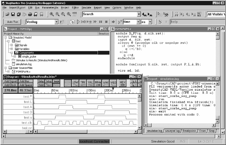
Figure C.4 Screenshot of VeriLogger Extreme running under the BugHunter graphical debugger.
C.4 USING SYNAPTICAD'S VERILOGGER EXTREME SIMULATOR
Install SynaptiCAD's VeriLogger Extreme Simulator located on the CDROM provided with the book or on SynaptiCAD's website at www.syncad.com. This installation is the evaluation version of the program, which is capable of simulating small Verilog projects and displaying the results. You may contact SynaptiCAD directly to purchase a full version (or student version) that can simulate larger models and save the results files.
Run VeriLogger Extreme:
- Choose Start > SynaptiCAD > Simulation Debug > VeriLogger Extreme + BugHunter menu to launch the simulator with the graphical debugger.
- Notice that the Help > BugHunter VeriLogger Manual menu launches a help program with the full simulator instructions.
- Also notice that Help > Tutorials > Basic Verilog Simulation is a tutorial on how to use the graphical interface and test-bench generation features of VeriLogger Extreme.
Create a project to store the list of files to be simulated:
- Choose the Project > New Project menu to open the New Project Wizard dialog (Figure C.5).
- In the Project Name box, type in FSM1, then click the Finish button. This will create a project file named FSMl.hpj in the directory specified.
Copy or Create-&-Add the source file to the project:
- Either copy the source file, by right clicking on the User Source Files Folder and choosing Copy HDL Files to Source File Folder from the context menu which will open a file dialog
Figure C.5 Project wizard screen.
Figure C.6 Showing how to copy source file of Listings C.1–C.4 to project.
(Figure C.6) and then use the browse button in the dialog to find the FSMSPWM.v on the CDROM.
- Or create a file called FSMSPWM.v by choosing the Editor > New HDL File menu option to open an editor window. Type in your source code printed in this appendix and save the file. Then add the file to the project by right clicking on the User Source Files Folder and choosing Add HDL Files to Source File Folder from the context menu.
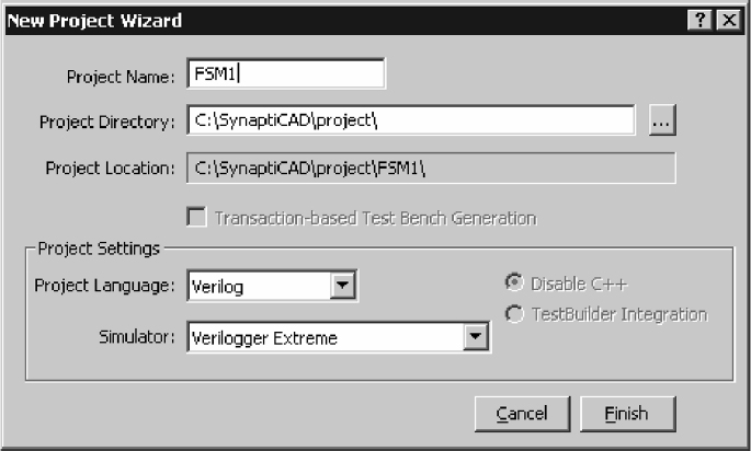

Figure C.7 Tool bar to build and simulate the code.

Figure C.8 Verilog simulator output waveforms.
- First, build the project by pressing the yellow Build button on the simulation button bar or selecting the Simulate > Build menu (Figure C.7).
- Building the project compiles the source files, fills the project window with the hierarchical structure of the design, and sets watches on all the signals and variables in the top-level component. A build will automatically be done each time the simulation is run, but having a separate build button enables you to create the project tree without having to wait for a simulation to run. After the build you are also able to set the top-level component for the project and/or select additional signals to watch using the project tree context menus. Watch signals are those listed in the Stimulus and Results diagram.
- Check the Report window to find any syntax errors found by the build.
- Next, start the simulator by pressing one of the green buttons on the Build and Simulate button bar. Section 2.1 Build and Simulate in the on-line help explains the differences between the types of single stepping and running.
- The simulated signals should appear in the Waveform window (Figure C.8).
- To produce waveforms with vertical transitions, first select the Options > Drawing Preferences menu to open a dialog, and then in the Edge Display section and check the Straight radio button.
C.5 SUMMARY
This tutorial looks at only one of many ways in which to develop a Verilog description of an FSM design. Other ways are discussed in Chapters 6–8. This tutorial also shows how you can use SynaptiCAD's VeriLogger Extreme simulator to verify your FSM design.
The design method is very easy to apply, with all the design information contained within the state diagram. This information can then be ‘extracted’ via the equations in order to synthesize a given design. The simulation of the circuit can then be used to confirm the design. The latest version of the software used in this tutorial can be downloaded free from SynaptiCAD at http://www.syncad.com. The version of VeriLogger Extreme may be updated from time to time, and a more recent copy of the demo version can be down loaded from the above website.