
1
Introduction to Finite-State Machines and State Diagrams for the Design of Electronic Circuits and Systems
1.1 INTRODUCTION
This chapter, and Chapters 2 and 3, is written in the form of a linear frame, programmed learning text. The reason for this is to help the reader to learn the basic skills required to design clocked finite-state machines (FSMs) so that they can develop their own designs based on traditional T flip-flops and D flip-flops. Later, other techniques will be introduced, such as One Hot, asynchronous FSMs, and Petri nets; these will be developed along the same lines as the work covered in this chapter, but not using the linear frame, programmed learning format.
The text is organized into frames, each frame following on consecutively from the previous one, but at times the reader may be redirected to other frames, depending upon the response to the questions asked. It is possible, however, to read the programmed learning chapters as a normal book.
There are tasks set throughout the frames to test your understanding of the material.
To make it easier to identify input and output signals, inputs will be in lowercase and outputs in uppercase.
Please read the Chapters 1–3 first and attempt all the questions before moving on to the later chapters. The reason for this approach is that the methods used in the book are novel, powerful, and when used correctly can lead to a rapid approach to the design of digital systems that use FSMs.
Chapters 1–5, 9 and 10 make use of techniques to develop FSM-based systems at the equation and gate level, where the designer has complete control of the design.
Chapters 6–8 can be read as a self-contained study of the Verilog hardware description language (HDL).
1.2 LEARNING MATERIAL
An FSM is a digital sequential circuit that can follow a number of predefined states under the control of one or more inputs. Each state is a stable entity that the machine can occupy. It can move from this state to another state under the control of an outside-world input.
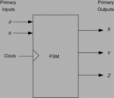
Figure 1.1 Block diagram of an FSM-based application.
Figure 1.1 shows an FSM with three outside-world inputs p, q, and the clock, and three outside-world outputs X, Y, and Z are shown. Note that some FSMs have a clock input and are called synchronous FSMs, i.e. those that do not belong to a type of FSM called asynchronous FSMs. However, most of this text will deal with the more usual synchronous FSMs, which do have a clock input. Asynchronous FSMs will be dealt with later in the book.
As noted above, inputs use lower case and output upper case names.
A synchronous FSM can move between states only if a clock pulse occurs.
| Task | Draw a block diagram for an FSM with five inputs x, y, z, t, and a clock, and with two outputs P and Q. |
Go to Frame 1.2 after attempting this question.
The FSM with five inputs x, y, z, t, and a clock, and with two outputs P and Q is shown in Figure 1.2.

Figure 1.2 Block diagram with inputs, outputs, and a clock input.
The reader may wish to go back and reread Frame 1.1 if the answer was incorrect.
Each state of the FSM needs to be identifiable. This is achieved by using a number of internal (to the FSM block) flip-flops. An FSM with four states would require two flip-flops, since two flip-flops can store 22 = 4 state numbers. Each state has aunique state number, and states are usually assigned numbers as s0 (state 0), s1, s2, and s3 (for the four-state example).
The rule here is
Number of states = 2Number of flip–flops,
for which
![]()
So an FSM with 13 states would require 24 flip-flops (i.e. 16 states, of which 13 are used in the FSM); that is:
![]()
This must be rounded up to the nearest integer, i.e. 4.
| Task |
|
After answering these questions, go to Frame 1.3.
The answers to the questions are as follows:
- How many flip-flops would be required for an FSM using 34 states?
26 = 64
would accommodate 34 states. In general:

- What would the state numbers be for this FSM?
These would be
s0, s1, s2, s3, s4, s5, s6, s7, s8, s9, s10, s11, s12, s13, s14, s15, s16, s17, s18, s19, s20, s21, s22, s23, s24, s25, s26, s27, s28, s29, s30, s31, s32, s33.
The unused states would be s34–s63.
Note, in this book, lower case‘s’ will be used to represent states to avoid confusion of state s0 with the word ‘so’ or ‘So’.
As well as containing flip-flops to define the individual states of the FSM uniquely, there is also combinational logic that defines the outside-world outputs. In addition, the outside-world inputs connect to combinational logic to supply the flip-flops inputs.
Go to Frame 1.4.
Figure 1.3 illustrates the internal architecture for a Mealy FSM.

Figure 1.3 Block diagram of a Mealy state machine structure.
This diagram shows that the FSM has a number of inputs that connect to the Next State Decoder (combinational) logic. The Q outputs of the memory element Flip-Flops connect to the Output Decoder logic, which in turn connects to the Outside World Outputs.
The Flip-Flops outputs are used as Next State inputs to the Next State Decoder, and it is these that determine the next state that the FSM will move to. Once the FSM has moved to this Next State, its Flip-Flops acquire a new Present State, as dictated by the Next State Decoder.
Note that some of the Outside World Inputs connect directly to the Output Decoder logic. This is the main feature of the Mealy-type FSM.
Go to Frame 1.5.
Another architectural form for an FSM is the Moore FSM.
The Moore FSM (Figure 1.4) differs from the Mealy FSM in that it does not have the feed-forward paths.
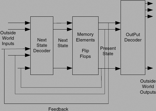
Figure 1.4 Block diagram of a Moore state machine structure.
This type of FSM is very common. Note that the Outside World Outputs are a function of the Flip-Flops outputs only (unlike the Mealy FSM architecture, where the Outside World Outputs are a function of Flip-Flops outputs and some Outside World Inputs).
Both the Moore and Mealy FSM designs will be investigated in this book.
Go to Frame 1.6.
Complete the following:
A Moore FSM differs to that of a Mealy FSM in that it has
_______________________________________________________________________________.
This means that the Moore FSM outputs depend on
_______________________________________________________________________________
_______________________________________________________________________________
whereas the Mealy FSM outputs can depend upon____________________________________.
Go back and read Frame 1.4 and Frame 1.5 for the solutions.
_______________________________________________________________________________.
Look at the Moore FSM architecture again, but with removal of all of the Outside World Inputs, apart from the clock. Also remove the Output Decoding logic. What is left should be a very familiar architecture. This is shown in Figure 1.5.

Figure 1.5 Block diagram of a Class C state-machine structure.
This architecture is in fact the synchronous counter that is used in many counter applications. Note that an Up/Down counter would have the additional outside-world input ‘Up/Down’, which would be used to control the direction of counting.
The Flip-Flops outputs in this architecture are used to connect directly to the outside-world. Note that, in a synchronous (clock-driven) FSM, one of the inputs would be the clock.
Go to Frame 1.8.
Historically, two types of state diagram have evolved: one for the design of Mealy FSMs and one for the design of Moore-type FSMs. The two are known as Mealy state diagrams and Moore state diagrams respectively.
These days, a more general type of state diagram can be used to design both the Mealy and Moore types of FSM. This is the type of state diagram that will be used throughout the remainder of this book.
A state diagram shows each state of the FSM and the transitions to and from that state to other states. The states are usually drawn as circles (but some people like to use a square box) and the transition between states is shown as an arrowed line connecting the states (Figure 1.6).

Figure 1.6 Transition between states.
In addition to the transitional line between states there is an input signal name (Figure 1.7).

Figure 1.7 Outside-world input to cause transition between states.
In the above diagram, the transition between state s0 and s1 will occur only if the Outside World Input st = 1 and a 0-to-1 transition occurs on the clock input.
| Task | What changes would be needed to the state diagram of Figure 1.9 to make the transition between s0 and s1 occur when input st = 0? |
After attempting this question, go to Frame 1.9.
The answer is shown in Figure 1.8.

Figure 1.8 Outside-world input between states.
Here, st has been replaced with /st, indicating that st must be logic 0 before a transition to s1 can take place), i.e. /st means ‘NOT st’; hence, when st = 0, /st = 1.
Note that outside-world inputs always lie along the transitional lines.
The state diagram must also show how the outside-world outputs are affected by the state diagram. This is achieved by placing the outside-world outputs either
- inside the state circle/square (Figure 1.9), or
- alongside the state circle/square.
In this diagram, outside-world outputs P and Q are shown inside the state circles. In this particular case, P is logic 1 in state s0, and changes to logic 0 when the FSM moves to state s1. Output Q does not change in the above transaction, remaining at logic 0 in both states.
Inputs like st are primary inputs; outputs like P and Q are primary outputs.
| Task | Draw a block diagram showing inputs and outputs for the state diagram of Figure 1.9. |
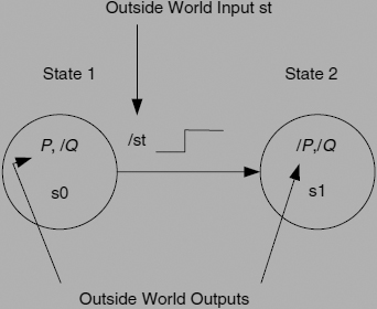
Figure 1.9 Showing placing of outside-world outputs.
Now go to Frame 1.10.
The block diagram will look like Figure 1.10.

Figure 1.10 The block diagram for state diagram of Figure 1.9.
This is easily obtained from the state diagram since inputs are located along transitional lines and outputs inside (or along side) the state circle.
Recall that in Frame 1.2 each state had to have a unique state number and that a number of flip-flops were needed to perform this task. These flip-flops are part of the internal design of the FSM and are used to produce an internal count sequence (they are essentially acting like a synchronous counter, but one that is controlled by the outside-world inputs). The internal count sequence produced by the flip-flops is used to control the outside-world decoder so that outputs can be turned on and off as the FSM moves between states.
In Frames 1.4 and 1.5 the architecture for the Mealy and Moore FSMs were shown. In both cases, the memory elements shown are the flip-flops discussed in the previous paragraph.
At this stage it is perhaps worth while looking at a simple FSM design in detail to see what it looks like. This will bring together all the ideas discussed so far, as well as introducing a few new ones. However, try answering the following questions before moving on to test your understanding so far:
| Tasks |
|
Go to Frame 1.11
Frame 1.11 Example of an FSM: a single-pulse generator circuit with memory
The idea here is to develop a circuit based on an FSM that will produce a single output pulse at its primary output P whenever its primary input s is taken to logic 1. In addition, a primary output L is to be set to logic 1 whenever input s is taken to logic 1, and cleared to logic 0 when the input s is released to logic 0. Output L acts as a memory indicator to indicate that a pulse has just been generated. The FSM is to be clock driven, so it also has an input clock. The block diagram of this circuit is shown in Figure 1.11.

Figure 1.11 Block diagram of single-pulse with memory FSM.
A suitable state diagram is shown in Figure 1.12.
In this state diagram the sling (loop going to and from s0) indicates that while input s is logic 0 (/s) the FSM will remain in state s0 regardless of how many clock pulses are applied to the FSM.
Only when input s goes to logic 1 (s) will the FSM move from state s0 to s1, and then only when a clock pulse arrives. Once in state s1, the FSM will set its outputs P and L to logic 1, and on the next clock pulse the FSM will move from state s1 to state s2.

Figure 1.12 State diagram for single-pulse with memory FSM.
The reason why the FSM will stay in state s1 for only one clock pulse is because, in state s1, the transition from this state to state s2 occurs on a clock pulse only. Once the FSM arrives in state s2 it will remain there whilst input s = 1. As soon as the input s goes to logic 0 (/s) the FSM will move back to state s0 on the next clock pulse.
Since the FSM remains in state s1 for only a single clock pulse, and since P = 1 only in state s1, the FSM will produce a single output pulse. Note that the memory indicator L will remain at logic 1 until s is released, so providing the user with an indication that a pulse has been generated.
Note in the FSM state diagram (Figure 1.12) that each state has a unique state identity s0, s1, and s2.
Note also that each state has been allocated a unique combination of flip-flop states:
- state s0 uses the flip-flop combination A = 0, B = 0, i.e. both flip-flops reset;
- state s1 uses the flip-flop combination A = 1, B = 0, i.e. flip-flop A is set;
- state s2 uses the flip-flop combination A = 0, B = 1, i.e.flip-flop A is reset, flip-flop B is set.
The A and B flip-flops values are known as the secondary state variables.
The flip-flop outputs are seen to define each state. The A and B outputs of the two flip-flops could be used to determine the state of the FSM from the state of the A and B flip-flops. The code sequence shown in Figure 1.12 follow a none unit distance coding, since more than one flip-flop changes state in some transitions.
Go to Frame 1.12.
Frame 1.12 The output signal states
It would also be possible to tell in which state the output P was to be logic 1, i.e. in state s1, where the flip-flop output logic levels are A = 1 and B = 0.
Therefore, the output P = A · /B (where the middot is the logical AND operation). Note that the flip-flops are used to provide a unique identity for each state.
Similarly, output L is logic 1 in states s1 and s2 and, therefore, L = s1 + s2.
L = s1 + s2 = A · /B + /A · B.
Also, see that since each state can be defined in terms of the flip-flop output states, the outside-world outputs can also be defined in terms of the flip-flop output states since the outside-world's output states themselves are a function of the states (P is logic one in state s1, and state s1 is defined in terms of the flip-flop outputs A · /B).
L is defined by A · /B + /A · B.
The allocation of unique values of flip-flop outputs is rather an arbitrary process. In theory, any values can be used so long as each state has a unique combination. This means that one cannot have more than one state with the flip-flop values of say A · /B.
In practice, it is common to assign flip-flop values so that the transition between each state involves only one flip-flop changing state. This is known as following a unit distance pattern. This has not been done in the example above because there are two flip-flop changes between states s1 and s2.
The single-pulse generator with memory state diagram could be made to follow a unit distance pattern by adding an extra state. This extra state could be inserted between states s2 and s0, having the same outputs for P and L as state s2.
Go to Frame 1.13.
The completed state diagram with unit distance patterns for flip-flops is shown in Figure 1.13.
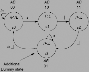
Figure 1.13 State diagram for single-pulse generator with memory.
Note that the added state has the unique name of s3 and the unique flip-flop assignment of A = 0 and B = 1. It also has the outputs P = 0, as it would be in state s0 (the state it is going to go to when s = 0). Also, L is retained at logic 1 until the input s is low, since L is the memory indicator and needs to be held high until the operator releases s.
In this design, the addition of the extra state has not added any more flip-flops to the design, since two flip-flops can have a maximum of 22 = 4 states (recall Frames 1.2 and 1.3).
The single pulse generator with memory FSM is to have an additional input added (called r) which will, when high (logic 1), cause the FSM to flash the P output at the clock rate. Whenever the r input is reverted to logic 0, the FSM will resume its single pulse with memory operation.
| Task |
|
Go to Frame 1.14 to see the result.
The block diagram is shown in Figure 1.14.

Figure 1.14 Block diagram for the FSM.
The new state diagram is shown in Figure 1.15.
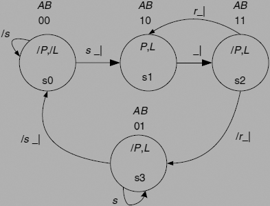
Figure 1.15 Single-pulse generator with multi-pulse feature.
The additional input has been added and a new transition from s2 to s1. Note that, when r = 1, the FSM is clocked between states s1 and s2. This will continue until r = 0.
In this condition, the P output will pulse on and off at the clock rate as long as input r is held at logic 1.
An alternative way of expressing output L
In the state diagram of Figure 1.15, L = s1 + s2 + s3 = A · /B + A · B + / A · B = A + /A · B. Therefore, L = A + B. See Appendix A and the auxiliary rule for the method of how this Boolean equation is obtained.
An alternative way of expressing L is in terms of its low state:
L = /(s0) = /(/A · /B).
This implies that when A = 0 and B = 0, L = 0.
Dealing with active-low signals
The state diagram fragment in Figure 1.16 illustrates how an active-low signal (in this case CS) that is low in states s4, s5 and s6 is obtained.

Figure 1.16 Dealing with active-low outputs.
Also, the active-low signal W is obtained as well. From this it can be inferred that, to obtain the active-low output, all states in which the output is low must be negated. This is a common occurrence in FSMs and will be used quite often.
Finally:
- If an output is high in more states than it is low, then the active-low equation might produce a minimal result.
- If the output is low in more states than it is high, then the active-high form of the output equation will produce the more minimal result.
Go to Frame 1.15.
The previous frames have considered the flip-flop output patterns. These are often referred to as the secondary state variables (Figure 1.17).

Figure 1.17 Block diagram showing secondary state variables in the FSM.
These are called secondary state variables because they are (from the FSM architecture viewpoint) internal to the FSM. Consider the Outside World inputs and outputs as being primary; then, it seems sensible to call the flip-flop outputs secondary state variables (state variables because they define the states of the state machine).
The outputs in the FSM are seen to be dependent upon the secondary state variables or flip-flops internal to the FSM. Looking back to Frame 1.5, see that Moore FSM outputs are dependent upon the flip-flop outputs only. The Output Decoding logic in the single-pulse generator with memory example is
P = s1 = A · /B
(see Frame 1.13) and
L = s1 + s2 + s3 = A · /B + A · B + /A · B = A + /A · B = A + B
(auxiliary rule again), i.e. it consists of one AND gate and an OR gate. This means that the single-pulse generator with memory design is a Moore FSM.
How could the single-pulse generator design be converted into a Mealy FSM?
One way would be to make the output P depend on the FSM being in state s1 (A. /B), but also gate it with the clock when it is low. This would make the P output have a pulse width equal to the clock pulse, but only in state s1, and only when the clock is low. This would be providing a feed-forward path from the (clock) input to the P (output).
| Task | How could the state diagram be modified to do this? |
Try modifying the state diagram, then go to Frame 1.16 to check the answer.
The modified state diagram is shown in Figure 1.18.

Figure 1.18 State diagram with Mealy output P.
Notice that, now, the output P is only equal to logic 1 when
- the FSM is in state s1 where flip-flop outputs are A = 1 and B = 0;
- the clock signal is logic 0.
The FSM enters state s1, where the P output will only be equal to logic 1 when the clock is logic 0. The clock will be logic 1 when the FSM enters state s1 (0-to-1 transition); it will then go to logic 0 (whilst still in state s1) and P will go to logic 1. Then, when the clock goes back to logic 1, the FSM will move to state s2 and the flip-flop outputs will no longer be A · /B, so the P output will go low again. Therefore, the P output will only be logic 1 for the time the clock is zero in state s1.
The timing diagram in Figure 1.19 illustrates this more clearly.
The waveforms show both versions of P (under the A and B waveforms in Figure 1.19). As can be seen, the Moore version raises P for the whole duration that the FSM is in state s1, whereas the Mealy version raises P for the time that the clock is low during state s1.
However, the bottom waveform for the Mealy P output illustrates what can happen as a result of a delay in the /clk signal, along with the change of state from s0 to s1(/A/B to A/B). Here, a glitch has been produced in the P signal as a result of the delay between clk and its complement /clk, after the A signal change. This is brought about by the clk signal causing A to change to logic 1 while the /clk signal is still at logic 1 due to the delay between the clk and / clk signals. This must be avoided.
This example is not unique; different delays can result in other unexpected outputs (glitches) from signal P. Essentially, if two signal changes occur, then a glitch can be produced in P as a result in the delays between signals (static 1 hazards).
Note that the P output signal is delayed in time as a result of the delays in signals A, B, and the /clk. This delay is not so important as long as it does not overrun the clock period (which in most practical cases it will not).

Figure 1.19 Timing diagram showing Moore and Mealy outputs.
It is best not to use the clock signal to create Mealy outputs. Also, as will be discussed in Chapter 3, it is wise, where possible, to use a unit distance coding for A and B variables to avoid two signal changes from occurring together; but more on this later.
Now for another example.
| Task | Produce a state diagram for an FSM that will generate a 101 pattern in response to m going high. The input m must be returned low before another 101 pattern can be produced. |
After attempting this task, go to Frame 1.17.
The solution to this problem is to use the basic arrangement of the single-pulse generator state diagram and insert more states to generate the required 101 pattern. This will be developed stage by stage so as to build up the complete design (Figure 1.20).
Start by first waiting for the input s to become logic 1. Therefore, in state s0, wait for s = 1. Once the input s =1 and the clock changes 0 to 1, the FSM is required to move into the next state s1, where P will be raised to the logic 1 level.
The next state s2 will be used to generate the required logic 0 at the P output. And then the next state s3 will be needed to generate the last P = 1.
Note that the FSM must leave state s3 on a clock pulse so that P = 1 for the duration of a single clock pulse only.

Figure 1.20 Development of the 101 pattern-generator sequence.
The final state required is to monitor for the input s = 0 condition. This state should return the FSM back to state s0.
| Task | Complete the FSM state diagram. |
Now go to Frame 1.18.
The completed state diagram is shown in Figure 1.21.

Figure 1.21 Complete state diagram for the 101 pattern-generator.
The Boolean equation for P in this diagram is P = s1 + s3. However, it is possible to make the P output a Mealy output that is only equal to one when in states s1 ands2, and only if an input y = 1.
Then:
P = s1 · y + s3 · y,
since P must be high in both states s1 and s3, but only when the input y is high.
A note on slings
A sling has been used for each state with an outside-world input along the transitional line. This is not really necessary, because slings are not used to obtain the circuits to perform the FSM function in modern state diagrams. In fact, they are really only included for cosmetic reasons, to improve the readability of the design. From now on, slings will only be used where they improve the readability of the state diagram.
| Task | Now try modifying the state diagram to make it produce a 1010 sequence of clock pulses (in the same manner shown in Figure 1.21, but with the P output pulse in state s3 to be conditional on a new input called x. If x = 0, the FSM should produce the output sequence 1000 at P. If x = 1, then the output sequence at P should be 1010. |
After drawing the state diagram, move to Frame 1.19.
The modified state diagram is shown in Figure 1.22.
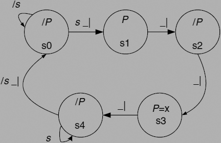
Figure 1.22 Modified state diagram with output P as a Mealy output.
In this state diagram, the input signal x is used as a qualifier in state s3 so that the output P is only logic 1 in this state when the clock is logic 1.
In state s3, the output P will only produce a pulse if the x input happens to be logic 1.
A pulse will always be produced in state s1.
It can be seen that if x = 0, then when the input s is raised to logic 1, the FSM will produce the sequence 1000 at output P.
If x = 1, then when s is raised to logic 1, the FSM will produce a 1010 sequence at the output P. This FSM is an example of a Mealy FSM, since the output P is a function of both the state and the input x, i.e. the input x is fed forward to the output decoding logic. Therefore, the equation for P is
P = s1 + s3 · x.
It would be easy to modify the FSM so that the 1000 sequence at P is produced if x = 1 and the 1010 sequence is produced if x = 0.
| Task |
|
After this, go to Frame 1.20.
The answer to Task 1 in Frame 1.19 is as follows: the Boolean equation for P which will produce a P 1010 sequence when x = 0 is
P = s1 + s3 · /x.
Note that in this case the qualifier for P is NOT x, rather than with x.
The answer to Task 2 in Frame 1.19, with regard to assigning a unit distance code to the state diagram, is shown in Figure 1.23.

Figure 1.23 State diagram with unit-distance coding of state variables.
The equation for P in s3 (it could be written outside the state circle if there is not enough room to show it inside the state circle) is conditional on the x input being logic 0. It is very likely that you will have come up with a different set of values for the secondary state assignments to those obtained here. This is perfectly all right, since there is no real preferred set of assignments, apart from trying to obtain a unit distance coding.
Some cheating has taken place here, since the transition between states s2 and s3 is not unit distance (since flip-flops A and C both change states). A unit distance coding could be obtained if an additional dummy state is added (as was the case in Frame 1.13 for the single-pulse generator with memory FSM).
However, in this example, one must be careful where one places the dummy state. If a dummy state is added between states s1 and s2, for example, then it would alter the P output sequence so that instead of producing, say, 1010, the sequence 10010 would be produced.
A safe place to add a dummy state would be between states s3 and s4, or between states s4 and s0, since they are outside the ‘critical’ P-sequence-generating part of the state diagram.
Move to Frame 1.21 for the timing waveform diagram solution.
The answer to Task 3 in Frame 1.19 is as follows.
A solution is shown in Figure 1.24 based on the secondary state assignment that was used earlier, so your solution could well be different.

Figure 1.24 Timing diagram showing the effect of input x on output P.
Note that in this solution the input x has been change to logic 0 in the middle of the clock pulse in state s3 just to illustrate the effect that this would have on the output P. Note that the output pulse on P is not a full clock high period in state s3.
This is a very realistic event, since the outside-world input x (indeed, any outside-world input) can occur at any time.
1.3 SUMMARY
At this point, the basics of what an FSM is and how a state diagram can be developed for a particular FSM design have been covered:
- how the outputs of the FSM depend upon the secondary state variables;
- that the secondary state variables can be assigned arbitrarily, but that following a unit distance code is good practice;
- a number of simple designs have shown how a Mealy or Moore FSM can be realized in the way in which the output equations are formed.
However, the state diagram needs to be realized as a circuit made up of logic gates and flip-flops; this part of the development process is very much a mechanized activity, which will be covered in Chapter 3.
Chapter 2 will look at a number of FSM designs that control outside-world devices in an attempt to provide some feel for the design of state diagrams for FSMs. The pace will be quicker, as it will be assumed that the preceding work has been understood.