CHAPTER 18
Line Inputs
External Signal Levels
There are several standards for line signal levels. The -10 dBV standard is used for a lot of semi-professional recording equipment, as it gives more headroom with unbalanced connections –the professional levels of +4 dBu and +6 dBu assume balanced outputs which inherently give twice the output level for the same supply rails, as it is measured between two pins with signals of opposite phase on them. See Table 18.1.
Signal levels in dBu are expressed with reference to 0 dBu = 775 mVrms; the origin of this odd value is that it gives a power of 1 mW in a purely historical 600 Ω load. The unit of dBm refers to the same level but takes the power in the load rather than the voltage as the reference– a distinction of little interest nowadays. Signal in dBV (or dBV) is expressed with reference to 0 dB = 1.000 Vrms.
These standards are well established, but that does not mean all equipment follows them. To take a current example, the Yamaha P7000S power amplifier requires +8 dBu (1.95 Vrms) to give its full output of 750W into 8Ω.
Internal Signal Levels
In any audio system, it is necessary to select a suitable nominal level for the signal passing through it. This level is always a compromise –the signal level should be high so it suffers minimal degradation by the addition of circuit noise as it passes through the system but not so high that it is likely to suffer clipping before the gain control or generate undue distortion below the clipping level. (This last constraint is not normally a problem with modern opamp circuitry, which gives very low distortion right up to the clipping point.)
It must always be considered that the gain control may be maladjusted by setting it too low and turning up the input level from the source equipment, making input clipping more likely. The internal levels chosen are usually in the range -6 to 0 dBu (388 mV to 775 mVrms), but in some specialised equipment such as broadcast mixing consoles, where levels are unpredictable and clipping distortion less acceptable than a bit more noise, the nominal internal level may be as low as–16 dBu (123 mVrms). If the internal level is in the normal -6 to 0 dBu range and the maximum output of an opamp is taken as 9 Vrms (+21.3 dBu), this gives from 27 to 20 dB of headroom before clipping occurs.
| Vrms | dBu | dBV | |
|---|---|---|---|
| Semi–professional | 0.316 | –7.78 | –10 |
| Professional | 1.228 | +4.0 | +1.78 |
| German ARD | 1.55 | +6.0 | +3.78 |
If the incoming signal does have to be amplified, this should be done as early as possible in the signal path to get the signal well above the noise floor as quickly as possible. If the gain is implemented in the first stage (i.e. the input amplifier, balanced or otherwise), the signal will be able to pass through later stages at a high level, so their noise contribution will be less significant. On the other hand, if the input stage is configured with a fixed gain, it will not be possible to turn it down to avoid clipping. Ideally, the input stage should have variable gain. It is not straightforward to combine this feature with a balanced input, but several ways of doing it are shown later in this chapter.
Input Amplifier Functions
First, RF filtering is applied at the very front end to prevent noise breakthrough and other EMC problems. It must be done before the incoming signal encounters any semiconductors where RF demodulation could occur and can be regarded as a “roofing filter”. At the same time, the bandwidth at the low end is given an early limit by the use of DC-blocking capacitors, and in some cases, overvoltage spikes are clamped by diodes. The input amplifier should present a reasonably high impedance to the outside world, not less than 10 kΩ, and preferably more. It must have a suitable gain –possibly switched or variable –to scale the incoming signal to the nominal internal level. Balanced input amplifiers also accurately perform the subtraction process that converts differential signals to single-ended ones, so noise produced by ground loops and the like is rejected. It’s quite a lot of work for one stage.
Unbalanced Inputs
The simplest unbalanced input feeds the incoming signal directly to the first stage of the audio chain. This is often impractical; for example, if the first stage was a Baxandall tone-control circuit, then the boost and cut curves would be at the mercy of whatever source impedance was feeding the input. In addition, the input impedance would be low and variable with frequency and control settings. Some sort of buffer amplifier that can be fed from a significant impedance without ill effect is needed.
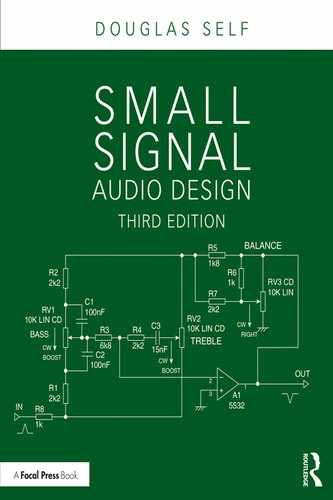
Figure 18.1 shows an unbalanced input amplifier, with the added components needed for interfacing to the real world. The opamp U1:A acts as a unity-gain voltage follower; it can be easily altered to give gain by adding two series feedback resistors. A 5532 bipolar type is used here for low noise; with the low source impedances that are likely to be encountered here, an FET-input opamp would be 10 dB or more noisier. R1 and C1 are a first-order low-pass filter to remove incoming RF before it has a chance to reach the opamp and demodulate into the audio band; once this has occurred, any further attempts at RF filtering are of course pointless. R1 and C1 must be as close to the input socket as physically possible to prevent RF from being radiated inside the box before it is shunted to ground and so come before all other components in the signal path.
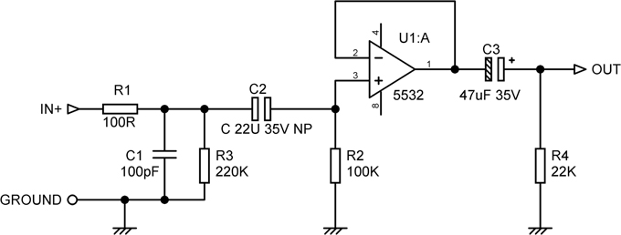
Figure 18.1 A typical unbalanced input amplifier with associated components.
Selecting component values for input filters of this sort is always a compromise, because the output impedance of the source equipment is not known. If the source is an active preamplifier stage, then the output impedance will probably be around 50 Ω, but it could be as high as 500 Ω or more. If the source is an oxymoronic “passive preamplifier” – i.e. just an input selector switch and a volume potentiometer –then the output impedance will be a good deal higher. (At least one passive preamplifier uses a transformer with switched taps for volume control; see Chapter 13.) If you really want to use a piece of equipment that embodies its internal contradictions in its very name, then a reasonable potentiometer value is 10 kΩ, and its maximum output impedance (when it is set for 6 dB of attenuation) will be 2.5 kΩ, which is very different from the 50 Ω we might expect from a good active preamplifier. This is in series with R1 and affects the turnover frequency of the RF filter. Effective RF filtering is very desirable, but it is also important to avoid a frequency response that sags significantly at 20 kHz. Valve equipment is also likely to have a high output impedance.
Taking 2.5 kΩ as a worst-case source impedance and adding R1, then 2.6 kΩ and 100 pF together give us -3 dB at 612 kHz; this gives a 20 kHz loss of only 0.005 dB, so possibly C1 could be usefully increased; for example, if we made it 220 pF, then the 20 kHz loss is still only 0.022 dB, but the -3 dB point is 278 kHz, much improving the rejection of what used to be called the Medium Wave. If we stick with C1 at 100 pF and assume an active output with a 50 Ω impedance in the source equipment, then together with the 100 Ω resistance of R1, the total is 150 Ω, which in conjunction with 100 pF gives us -3 dB at 10.6 MHz. This is rather higher than desirable, but it is not easy to see what to do about it, and we must accept the compromise. If there was a consensus that the output impedance of a respectable piece of audio equipment should not exceed 100 Ω, then things would be much easier.
Our compromise seems reasonable, but can we rely on 2.5 kΩ as a worst-case source impedance? I did a quick survey of the potentiometer values that passive preamplifiers currently employ, and while it confirmed that 10 kΩ seems to be the most popular value, one model had a 20 kΩ potentiometer, and another had a 100 kΩ pot. The latter would have a maximum output impedance of 25 kΩ and would give very different results with a C1 value of 100 pF –the worst-case frequency response would now be -3 dB at 63.4 kHz and –0.41 dB at 20 kHz, which is not helpful if you are aiming for a ruler-flat response in the audio band.
To put this into perspective, filter capacitor C1 will almost certainly be smaller than the capacitance of the interconnecting cable. Audio interconnect capacitance is usually in the range 50 to 150 pF/metre, so with our assumed 2.5 kΩ source impedance and 150 pF/metre cable, and ignoring C1, you can only permit yourself a rather short run of 3.3 metres before you are –0.1 dB down at 20 kHz, while with a 25 kΩ source impedance, you can hardly afford to have any cable at all; if you use low-capacitance 50 pF/metre cable, you might just get away with a metre. This is just one of many reasons why “passive preamplifiers” really are not a good idea.
Another important consideration is that the series resistance R1 must be kept as low as practicable to minimise Johnson noise; but lowering this resistance means increasing the value of shunt capacitor C1, and if it becomes too big, then its impedance at high audio frequencies will become too low. Not only will there be too low a roll-off frequency if the source has a high output impedance, but there might be an increase in distortion at high audio frequencies because of excessive loading on the source output stage.
Replacing R1 with a small inductor to make an LC low-pass filter will give much better RF rejection at increased cost. This is justifiable in professional audio equipment, but it is much less common in hi-fi, one reason being that the unpredictable source impedance makes the filter design difficult, as we have just seen. In the professional world, one can assume that the source impedance will be low. Adding more capacitors and inductors allows a 3- or 4-pole LC filter to be made. If you do use inductors then it is essential to check the frequency response to make sure it is what you expect and there is no peaking at the turnover frequency.
C2 is a DC-blocking capacitor to prevent voltages from ill-conceived source equipment getting into the circuitry. It is a non-polarised type, as voltages from the outside world are of unpredictable polarity, and it is rated at not less than 35 V so that even if it gets connected to defective equipment with an opamp output jammed hard against one of the supply rails, no harm will result. R3 is a DC drain resistor that prevents the charge put on C2 by the aforesaid external equipment from remaining there for a long time and causing a thud when connections are replugged; as with all input drain resistors, its value is a compromise between discharging the capacitor reasonably quickly and keeping the input impedance acceptably high. The input impedance here is R3 in parallel with R2, i.e. 220 kΩ in parallel with 100 kΩ, giving 68 kΩ. This is a good high value and should work well with just about any source equipment you can find, including valve technology.
R2 provides the biasing for the opamp input; it must be a high value to keep the input impedance up, but bipolar-input opamps draw significant input bias current. The Fairchild 5532 data sheet quotes 200 nA typical and 800 nA maximum, and these currents would give a voltage drop across R2 of 20 mV and 80 mV, respectively. This offset voltage will be reproduced at the output of the opamp, with the input offset voltage added on; this is only 4 mV maximum and so will not affect the final voltage much, whatever its polarity. The 5532 has NPN input transistors, and the bias current flows into the input pins, so the voltage at Pin 3 and hence the output will be negative with respect to ground by anything up to 84 mV.
Such offset voltages are not so great that the output voltage swing of the opamp is significantly affected, but they are enough to generate unpleasant clicks and pops if the input stage is followed by any sort of switching and enough to make potentiometers crackly. Output DC blocking is therefore required in the shape of C3, while R4 is another DC drain resistor to keep the output at zero volts. It can be made rather lower in value than the input drain resistor R3, as the only requirement is that it should not significantly load the opamp output. FET-input opamps have much lower input bias currents so that the offsets they generate as they flow through biasing resistors are usually negligible, but they still have input offset voltages of a few millivolts, so DC blocking will still be needed if switches downstream are to work silently.
This input stage, with its input terminated by 50 Ω to ground, has a noise output of only -119.0 dBu over the usual 22–22 kHz bandwidth. This is very quiet indeed and is a reflection of the fact that R1, the only resistor in the signal path, has the low value of 100 Ω and so generates a very small amount of Johnson noise, only -132.6 dBu. This is swamped by the voltage noise of the opamp, which is basically all we see; its current noise has negligible effect because of the low circuit impedances.
Balanced Interconnections
Balanced inputs are used to prevent noise and crosstalk from affecting the input signal, especially in applications in which long interconnections are used. They are standard on professional audio equipment and are slowly but steadily becoming more common in the world of hi-fi. Their importance is that they can render ground loops and other connection imperfections harmless. Since there is no point in making a wonderful piece of equipment and then feeding it with an impaired signal, making an effective balanced input is of the first importance.
The basic principle of balanced interconnection is to get the signal you want by subtraction, using a three-wire connection. In some cases, a balanced input is driven by a balanced output, with two anti-phase output signals; one signal wire (the hot or in-phase) sensing the in-phase output of the sending unit, while the other senses the anti-phase output.
In other cases, when a balanced input is driven by an unbalanced output, as shown in Figure 18.2, one signal wire (the hot or in phase) senses the single output of the sending unit, while the other (the cold or phase inverted) senses the unit’s output-socket ground, and once again the difference between them gives the wanted signal. In either of these two cases, any noise voltages that appear identically on both lines (i.e. common-mode signals) are in theory completely cancelled by the subtraction. In real life, the subtraction falls short of perfection, as the gains via the hot and cold inputs will not be precisely the same, and the degree of discrimination actually achieved is called the common-mode rejection ratio, of which more later.
Figure 18.2 Unbalanced output to balanced input interconnection.
It is deeply tedious to keep referring to non-inverting and inverting inputs, and so these are usually abbreviated to “hot” and “cold”, respectively. This does not necessarily mean that the hot terminal carries more signal voltage than the cold one. For a true balanced connection, the voltages will be equal. The “hot” and “cold” terminals are also often referred to as IN+ and IN-, and this latter convention has been followed in the diagrams here.
The subject of balanced interconnections is a large one, and a big book could be written on this topic alone; one of the classic papers on the subject is by Muncy. [1] To make a start, let us look at the pros and cons of balanced connections.
The Advantages of Balanced Interconnections
- Balanced interconnections discriminate against noise and crosstalk, whether they result from ground currents or electrostatic or magnetic coupling to signal conductors.
- Balanced connections make ground loops much less intrusive and usually inaudible, so people are less tempted to start “lifting the ground” to break the loop, with possibly fatal consequences. This tactic is only acceptable if the equipment has a dedicated ground-lift switch that leaves the external metalwork firmly connected to mains safety earth. In the absence of this switch, the foolhardy and optimistic will break the mains earth (not quite so easy now that moulded mains plugs are standard), and this practice is of course highly dangerous, as a short circuit from mains to the equipment chassis will result in live metalwork but dead people.
- A balanced interconnection incorporating a true balanced output gives 6 dB more signal level on the line, which should give 6 dB more dynamic range. However, this is true only with respect to external noise –as is described later in this chapter, a standard balanced input using 10 kΩ resistors is about 14 dB noisier than the unbalanced input shown in Figure 18.1 above.
- Balanced connections are usually made with XLR connectors. These are a professional three-pin format and are far superior to the phono (RCA) type normally used for unbalanced connections. More on this below.
The Disadvantages of Balanced Interconnections
- Balanced inputs are almost always noisier than unbalanced inputs by a large margin in terms of the noise generated by the input circuitry itself rather than external noise. This may appear paradoxical, but it is all too true, and the reasons will be fully explained in this chapter.
- More hardware means more cost. Small-signal electronics is relatively cheap; unless you are using a sophisticated low-noise input stage, of which more later, most of the extra cost is likely to be in the balanced input connectors.
- Balanced connections do not of themselves provide any greater RF immunity than an unbalanced input. For this to happen, both legs of the balanced input would have to demodulate the RF in equal measure for common-mode cancellation to occur. This is highly unlikely, and the chances of it happening over a wide frequency range are zero. It remains vital to provide the usual passive RF filtering in front of any electronics to avoid EMC troubles.
- There is the possibility of introducing a phase error. It is all too easy to create an unwanted phase inversion by confusing hot and cold when wiring up a connector, and this can go undiscovered for some time. The same mistake on an unbalanced system interrupts the audio completely and leaves no room for doubt.
Balanced Cables and Interference
In a balanced interconnection, two wires carry the signal, and the third connection is the ground wire, which has two functions. First, it joins the grounds of the interconnected equipment together. This is not always desirable, and if galvanic isolation is required, a transformer balancing system will be necessary, because the large common-mode voltages are likely to exceed the range of an electronic balanced input. A good transformer will also have a very high CMRR, which will be needed to get a clean signal in the face of large CM voltages.
Second, the presence of the ground allows electrostatic screening of the two signal wires, preventing both the emission and pick-up of unwanted signals. This can mean:
- A lapped screen, with wires laid parallel to the central signal conductor. The screening coverage is not total and can be badly degraded, as the screen tends to open up on the outside of cable bends. Not recommended unless cost is the dominating factor.
- A braided screen around the central signal wires. This is much more expensive, as it is harder to make, but it opens up less on bending than a lap screen. Even so, screening is not 100%. It has to be said that it is a pain to terminate in the usual audio connectors. Not recommended.
- An overlapping foil screen, with the ground wire (called the drain wire in this context for some reason) running down the inside of the foil and in electrical contact with it. This is usually the most effective, as the foil is a solid sheet and cannot open up on the outside of bends. It should give perfect electrostatic screening, and it is much easier to work with than either lap screen or braided cable. However, the higher resistance of aluminium foil compared with copper braid means that RF immunity may not be so good.
There are three main ways in which an interconnection is susceptible to hum and noise.
An interfering signal at significant voltage couples directly to the inner signal line, through stray capacitance. The stray capacitance between imperfectly screened conductors will be a fraction of a pF in most circumstances, as electrostatic coupling falls off with the square of distance. This form of coupling can be serious in studio installations with unrelated signals running down the same ducting.
The three main lines of defence against electrostatic coupling are effective screening, low impedance drive, and a good CMRR maintained up to the top of the audio spectrum. As regards screening, an overlapped foil screen provides complete protection.
Driving the line from a low impedance, of the order of 100 Ω or less, is also helpful because the interfering signal, having passed through a very small stray capacitance, is a very small current and cannot develop much voltage across such a low impedance. This is convenient because there are other reasons for using a low output impedance, such as optimising the interconnection CMRR, minimising HF losses due to cable capacitance, and driving multiple inputs without introducing gain errors. For the best immunity to crosstalk, the output impedance must remain low up to as high a frequency as possible. This is definitely an issue, as opamps invariably have a feedback factor that begins to fall from a low and quite possibly sub-audio frequency, and this makes the output impedance rise with frequency as the negative feedback factor falls, as if an inductor were in series. Some line outputs have physical series inductors to improve stability or EMC immunity, and these should not be so large that they significantly increase the output impedance at 20 kHz. From the point of view of electrostatic screening alone, the screen does not need to be grounded at both ends, or form part of a circuit. [2] It must of course be grounded at some point.
If the screening is imperfect and the line impedance non-zero, some of the interfering signal will get into the hot and cold conductors, and now the CMRR must be relied upon to make the immunity acceptable. If it is possible, rearranging the cable run away from the source of interference and getting some properly screened cable is more practical and more cost effective than relying on very good common-mode rejection.
Stereo hi-fi balanced interconnections almost invariably use XLR connectors. Since an XLR can only handle one balanced channel, two separate cables are almost invariably used, and interchannel capacitive crosstalk is not an issue. Professional systems, on the other hand, use multi-way connectors that do not have screening between the pins, and there is an opportunity for capacitive crosstalk here, but the use of low source impedances should reduce it to below the noise floor.
If a cable runs through an AC magnetic field, an EMF is induced in both signal conductors and the screen, and according to some writers, the screen current must be allowed to flow freely, or its magnetic field will not cancel out the field acting on the signal conductors, and therefore the screen should be grounded at both ends, to form a circuit. [3] In practice, the magnetic field cancellation will be very imperfect, and reliance is better placed on the CMRR of the balanced system to cancel out the hopefully equal voltages induced in the two signal wires. The need to ground both ends to possibly optimise the magnetic rejection is not usually a restriction, as it is rare that galvanic isolation is required between two pieces of audio equipment.
The equality of the induced voltages can be maximised by minimising the loop area between the hot and cold signal wires, for example by twisting them tightly together in manufacture. In practice, most audio foil-screen cables have parallel rather than twisted signal conductors, but this seems adequate almost all of the time. Magnetic coupling falls off with the square of distance, so rearranging the cable run away from the source of magnetic field is usually all that is required. It is unusual for it to present serious difficulties in a hi-fi application.
3. Ground Voltages
These are the result of current flowing through the ground connection and are often called “common-impedance coupling” in the literature. [1] This is the root of most ground-loop problems. The existence of a loop in itself does no harm, but it is invariably immersed in a 50 Hz magnetic field that induces mains-frequency currents plus harmonics into it. This current produces a voltage drop down non-negligible ground-wire resistances, and this effectively appears as a voltage source in each of the two signal lines. Since the CMRR is finite, a proportion of this voltage will appear to be a differential signal and will be reproduced as such.
Balanced Connectors
Balanced connections are most commonly made with XLR connectors, though it can be done with stereo (tip-ring-sleeve) jack plugs. XLRs are a professional three-pin format and are much better connectors in every way than the usual phono (RCA) connectors used for unbalanced interconnections. Phono connectors have the great disadvantage that if you are connecting them with the system active (inadvisable, but then people are always doing inadvisable things), the signal contacts meet before the grounds, and thunderous noises result. The XLR standard has Pin 2 as hot, Pin 3 as cold, and Pin 1 as ground.
Stereo jack plugs are often used for line level signals in a recording environment and are frequently found on the rear of professional power amplifiers as an alternative to an adjacent XLR connector. Both full-size and 3.5 mm sizes are used. Balanced jacks are wired with the tip as hot, the ring as cold, and the sleeve as ground. Sound reinforcement systems often use large multi-way connectors that carry dozens of three-wire balanced connections.
Balanced Signal Levels
Many pieces of equipment, including preamplifiers and power amplifiers designed to work together, have both unbalanced and balanced inputs and outputs. The general consensus in the hi-fi world is that if the unbalanced output is, say, 1 Vrms, then the balanced output will be created by feeding the in-phase output to the hot output pin and also to a unity-gain inverting stage, which drives the cold output pin with 1 Vrms phase inverted. The total balanced output voltage between hot and cold pins is therefore 2 Vrms, and so the balanced input must have a gain of ½ or -6 dB relative to the unbalanced input to maintain consistent internal signal levels.
Electronic Versus Transformer Balanced Inputs
Balanced interconnections can be made using either transformer or electronic balancing. Electronic balancing has many advantages, such as low cost, low size and weight, superior frequency and transient response, and no low-frequency linearity problems. It may still be regarded as a second-best solution in some quarters, but the performance is more than adequate for most professional applications. Transformer balancing does have some advantages of its own, particularly for work in very hostile RF/EMC environments, but serious drawbacks. The advantages are that transformers are electrically bulletproof, retain their high CMRR performance forever, and consume no power even at high signal levels. They are essential if galvanic isolation between ground is required. Unfortunately, transformers generate LF distortion, particularly if they have been made with minimal core sizes to save weight and cost. They are liable to have HF response problems due to leakage reactance and distributed capacitance, and compensating for this requires a carefully designed Zobel network across the secondary. Inevitably, they are heavy and expensive. Transformer balancing is therefore relatively rare, even in professional audio applications, and the greater part of this chapter deals with electronically balanced inputs.
Common Mode Rejection
Figure 18.3 shows a balanced interconnection reduced to its bare essentials; hot and cold line outputs with source resistances Rout+, Rout- and a standard differential amplifier at the input end. The output resistances are assumed to be exactly equal, and the balanced input in the receiving equipment has two exactly equal input resistances to ground R1, R2. The ideal balanced input amplifier senses the voltage difference between the points marked IN+ (hot) and IN- (cold) and ignores any common-mode voltage which is present on both. The amount by which it discriminates is called the common-mode rejection ratio or CMRR, and is usually measured in dB. Suppose a differential voltage input between IN+ and IN- gives an output voltage of 0 dB; now reconnect the input so that IN+ and IN- are joined together, and the same voltage is applied between them and ground. Ideally, the result would be zero output, but in this imperfect world, it won’t be, and the output could be anywhere between -20 dB (for a bad balanced interconnection, which probably has something wrong with it) and -140 dB (for an extremely good one). The CMRR when plotted may have a flat section at low frequencies, but it very commonly degrades at high audio frequencies and may also deteriorate at very low frequencies. More on that later.
In one respect, balanced audio connections have it easy. The common-mode signal is normally well below the level of the unwanted signal, and so the common-mode range of the input is not an issue. In other areas of technology, such as electrocardiogram amplifiers, the common-mode signal may be many times greater than the wanted signal.

The simplified conceptual circuit of Figure 18.3, under SPICE simulation, demonstrates the need to get the resistor values right for a good CMRR before you even begin to consider the rest of the circuitry. The differential voltage sources Vout+, Vout-, which represents that the actual balanced outputs are set to zero, and Vcm, which represents the common-mode voltage drop down the cable ground, is set to 1 volt to give a convenient result in dBV. The output resulting from the presence of this voltage source is measured by a mathematical subtraction of the voltages at IN+ and IN-, so there is no actual input amplifier to confuse the results with its non-ideal performance.
Let us begin with Rout+ and Rout- set to 100 Ω and R1 and R2 set to 10 kΩ. These are typical real-life values as well as being nice round figures. When all four resistances are exactly at their nominal value, the CMRR is in theory infinite, which my SPICE simulator rather curiously reports as exactly -400 dB. If one of the output resistors or one of the input resistors is then altered in value by 1%, then the CMRR drops like a stone to -80 dB. If the deviation from equality is 10%, things are predictably worse, and the CMRR degrades to -60 dB, as shown in Table 18.2. That would be quite a good figure in reality, but since we have not yet even thought about opamp imperfections or other circuit imbalances and have only altered one resistance out of the four that will in real circuitry all have their own tolerances, it underlines the need to get things right at the most basic theoretical level before we dig deeper into the circuitry. The CMRR is naturally flat with frequency because our simple model has no frequency-dependent components.
The essence of the problem is that we have two resistive dividers, and to get an infinite CMRR, they must have exactly the same attenuation. If we increase the ratio between the output and input resistors by reducing the former or increasing the latter, the attenuation factor becomes closer to unity, so variations in either resistor value have less effect on it. If we increase the input impedance to 100 kΩ, which is quite practical in real life (we will put aside the noise implications of this for the moment), things are 10 times better, as the Rin/Rout ratio has improved from 100 to 1000 times. We now get a CMRR of -100 dB with a 1% resistance deviation and -80 dB with a 10% deviation. An even higher input impedance of 1 MΩ, which is perhaps a bit less practical, raises Rin/Rout to 10,000 and gives -120 dB for a 1% resistance deviation and -100 dB for a 10% deviation.
| Rout+ | Rout- | Rout Deviation | R1 | R2 | R1, R2 deviation | Rin/Rout ratio | CMRR dB |
|---|---|---|---|---|---|---|---|
| 100 | 100 | 0 | 10k | 10k | 0 | 100 | Infinity |
| 100 | 101 | 1% | 10k | 10k | 0 | 100 | –80.2 |
| 100 | 110 | 10% | 10k | 10k | 0 | 100 | –60.2 |
| 100 | 100 | 0 | 10k | 10.1k | 1% | 100 | –80.3 |
| 100 | 100 | 0 | 10k | 11k | 10% | 100 | –61.0 |
| 100 | 100 | 0 | 100k | 101k | 1% | 1000 | –100.1 |
| 100 | 100 | 0 | 100k | 110k | 10% | 1000 | –80.8 |
| 100 | 100 | 0 | 1M | 1.01M | 1% | 10,000 | –120.1 |
| 100 | 100 | 0 | 1M | 1.1M | 10% | 10,000 | –100.8 |
| 68 | 68 | 0 | 20k | 20.2k | 1% | 294 | –89.5 |
| 68 | 68 | 0 | 20k | 22k | 10% | 294 | –70.3 |
We can attack the other aspect of the attenuation problem by reducing the output impedances to 10 Ω, ignoring for the moment the need to secure against HF instability caused by cable capacitance, and also return the input impedance resistors to 100 kΩ. Rin/Rout is 10,000 once more, and as you might suspect, the CMRR is once more -120 dB for a 1% deviation and -100 dB for a 10% deviation. Ways to make stable output stages with very low output impedances are described in Chapter 19; a fraction of an Ohm at 1 kHz is quite easy to achieve.
In conventional circuits, the combination of 68 Ω output resistors and a 20 kΩ input impedance is often encountered, 68Ω being about as low as you want to go if HF instability is to be absolutely guarded against with the long lines used in professional audio. The 20 kΩ common-mode input impedance is what you get if you make a basic balanced input amplifier with four 10 kΩ resistors. I strongly suspect that this value is so popular because it looks as if it gives standard 10 kΩ input impedances –in fact, it does nothing of the sort, and the common-mode input impedance, which is what matters here, is 20 kΩ on each leg; more on that later. It turns out that 68 Ω output resistors and a 20 kΩ input impedance give a theoretical CMRR of -89.5 dB for a 1% deviation of one resistor, which is quite encouraging. These results are summarised in Table 18.2.
The conclusion is simple: we need the lowest possible output impedances and the highest possible input impedances to get the maximum common-mode rejection. This is highly convenient, because low output impedances are already needed to drive multiple amplifier inputs and cable capacitance, and high input impedances are needed to minimise loading and maximise the number of amplifiers that can be driven.
The Basic Electronic Balanced Input
Figure 18.4 shows the basic balanced input amplifier using a single opamp. To achieve balance, R1 must be equal to R3 and R2 equal to R4. It has a gain of R2/R1 (=R4/R3). The standard one-opamp balanced input or differential amplifier is a very familiar circuit block, but its operation often appears somewhat mysterious. Its input impedances are not equal when it is driven from a balanced output; this has often been commented on [4], and some confusion has resulted.
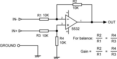
The source of the confusion is that a simple differential amplifier has interaction between the two inputs, so that the input impedance seen on the cold input depends on the signal applied to the hot input. Input impedance is measured by applying a signal and seeing how much current flows into the input, so it follows that the apparent input impedance on each leg varies according to how the cold input is driven. If the amplifier is made with four 10 kΩ resistors, then the input impedances on hot and cold are as shown in Table 18.3:
Some of these impedances are not exactly what you might expect and require some explanation.
Case 1
The balanced input is being used as an unbalanced input by grounding the cold input and driving the hot input only. The input impedance is therefore simply R3 + R4. Resistors R3 and R4 reduce the signal by a factor of a half, but this loss is undone as R1 and R2 set the amplifier gain to two times, and the overall gain is unity. If the cold input is not grounded, then the gain is 0.5 times. The attenuate-then-amplify architecture plus the Johnson noise from the resistors makes this configuration much noisier than the dedicated unbalanced input of Figure 18.1, which has only a single 100 Ω resistor in the signal path.
| Case | Pins driven | Hot input res Ω | Cold input res Ω |
|---|---|---|---|
| 1 | Hot only | 20k | Grounded |
| 2 | Cold only | Grounded | 10k |
| 3 | Both (balanced) | 20k | 6.66k |
| 4 | Both common–mode | 20k | 20k |
| 5 | Both floating | 10k | 10k |
Case 2
The balanced input is again being used as an unbalanced input, but this time by grounding the hot input and driving the cold input only. This gives a phase inversion, and it is unlikely you would want to do it except as an emergency measure to correct a phase error somewhere else. The important point here is that the input impedance is now only 10 kΩ, the value of R1, because shunting negative feedback through R2 creates a virtual earth at Pin 2 of the opamp. Clearly this simple circuit is not as symmetrical as it looks. The gain is unity, whether or not the hot input is grounded; grounding it is desirable because it not only prevents interference being picked up on the hot input pin but also puts R3 and R4 in parallel, reducing the resistance from opamp Pin 3 to ground and so reducing Johnson noise and the effects of opamp current noise.
Case 3
This is the standard balanced interconnection. The input is driven from a balanced output with the same signal levels on hot and cold, as if from a transformer with its centre-tap grounded, or an electronically balanced output using a simple inverter to drive the cold pin. The input impedance on the hot input is what you would expect; R3 + R4 add up to 20 kΩ. However, on the cold input, there is a much lower input impedance of 6.66 kΩ. This at first sounds impossible, as the first thing the signal encounters is a 10 kΩ series resistor, but the crucial point is that the hot input is being driven simultaneously with a signal of the opposite phase, so the inverting opamp input is moving in the opposite direction to the cold input due to negative feedback, and what you might call anti-bootstrapping reduces the effective value of the 10 kΩ resistor to 6.66 kΩ. These are the differential input impedances we are examining, the impedances seen by the balanced output driving them. Common-mode signals see a common-mode impedance of 20 kΩ, as in Case 4.
You will sometimes see the statement that these unequal differential input impedances “unbalance the line”. From the point of view of CMRR, this is not the case, as it is the CM input impedance that counts. The line is, however, unbalanced in the sense that the cold input draws three times the current from the output that the hot one does. This current imbalance might conceivably lead to inductive crosstalk in some multi-way cable situations, but I have never encountered it. The differential input impedances can be made equal by increasing the R1 and R2 resistor values by a factor of three, but this degrades the noise performance markedly and makes the common-mode impedances to ground unequal, which is a much worse situation, as it compromises the rejection of ground voltages, and these are almost always the main problem in real life.
Case 4
Here both inputs are driven by the same signal, representing the existence of a common-mode voltage. Now both inputs show an impedance of 20 kΩ. It is the symmetry of the common-mode input impedances that determines how effectively the balanced input rejects the common-mode signal. This configuration is of course only used for CMRR testing.
Case 5
Now the input is driven as from a floating transformer with the centre-tap (if any) unconnected, and the impedances can be regarded as equal; they must be, because with a floating winding, the same current must flow into each input. However, in this connection, the line voltages are not equal and opposite: with a true floating transformer winding, the hot input has all the signal voltage on it while the cold has none at all due to the negative feedback action of the balanced input amplifier. This seemed very strange when it emerged in SPICE simulation, but a sanity check with real components proves it true. The line has been completely unbalanced as regards crosstalk to other lines, although its own common-mode rejection remains good.
Even if absolutely accurate resistors are assumed, the CMRR of the stage in Figure 18.4 is not infinite; with a TL072, it is about -90 dB, degrading from 100 Hz upwards, due to the limited open-loop gain of the opamp. We will now examine this effect.
The Basic Balanced Input and Opamp Effects
In the earlier section on CMRR, we saw that in a theoretical balanced line, choosing low output impedances and high input impedances would give very good CM rejection even if the resistors were not perfectly matched. Things are a bit more complex (i.e. worse) if we replace the mathematical subtraction with a real opamp. We quickly find that even if perfectly matched resistors everywhere are assumed, the CMRR of the stage is not infinite, because the two opamp inputs are not at exactly the same voltage. The negative feedback error-voltage between the inputs depends on the open-loop gain of the opamp, and that is neither infinite nor flat with frequency into the far ultra-violet. Far from it. There is also the fact that opamps themselves have a common-mode rejection ratio; it is high, but once more, it is not infinite.
As usual, SPICE simulation is instructive, and Figure 18.5 shows a simple balanced interconnection, with the balanced output represented simply by two 100 Ω output resistances connected to the source equipment ground, here called Ground 1, and the usual differential opamp configuration at the input end, where we have Ground 2.

A common-mode voltage Vcm is now injected between Ground 1 and Ground 2, and the signal between the opamp output and Ground 2 is measured. The balanced input amplifier has all four of its resistances set to precisely 10 kΩ, and the opamp is represented by a very simple model that has only two parameters; a low-frequency open-loop gain, and a single pole frequency that says where that gain begins to roll off at 6 dB per octave. The opamp input impedances and the opamp’s own CMRR are assumed infinite, as in the world of simulation, they so easily can be. Its output impedance is set at zero.
| Open-loop gain | CMRR dB | CMRR ratio |
|---|---|---|
| 10,000 | –74.0 | 19.9 ×10⁻⁵ |
| 30,000 | –83.6 | 66.4 × 10⁻⁶ |
| 100,000 | –94.0 | 19.9 × 10⁻⁶ |
| 300,000 | –103.6 | 6.64 × 10⁻⁶ |
| 1,000,000 | –114.1 | 1.97 × 10⁻⁶ |
For the first experiments, even the pole frequency is made infinite, so now the only contact with harsh reality is that the opamp open-loop gain is finite. That is, however, enough to give distinctly non-ideal CMRR figures, as Table 18.4 shows:
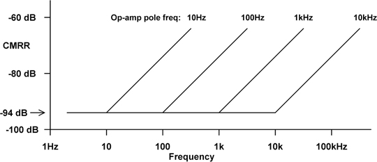
With a low-frequency open-loop gain of 100,000, which happens to be the typical figure for a 5532 opamp, even perfect components everywhere will never yield a better CMRR than -94 dB. The CMRR is shown as a raw ratio in the third column, so you can see that the CMRR is inversely proportional to the gain, and so we want as much gain as possible.
Opamp Frequency Response Effects
To examine these, we will set the low-frequency gain to 100,000, which gives a CMRR “floor” of -94 dB, and then introduce the pole frequency that determines where it rolls-off. The CMRR now worsens at 6 dB/octave, starting at a frequency set by the interaction of the low-frequency gain and the pole frequency. The results are summarised in Table 18.5, which shows that as you might expect, the lower the open-loop bandwidth of the opamp, the lower the frequency at which the CMRR begins to fall off. Figure 18.6 shows the situation diagrammatically.
Table 18.6 gives the open-loop gain and pole parameters for a few opamps of interest. Both parameters, but especially the gain, are subject to considerable variation; the typical values from the manufacturers’ data sheets are given here.
Some of these opamps have very high open-loop gains, but only at very low frequencies. This may be good for DC applications, but in audio line input applications, where the lowest frequency of CMRR interest is 50 Hz, they will be operating above the pole frequency, and so the gain available will be less –possibly considerably so in the case of opamps like the OPA2134. This is not, however, a real limitation, for even if a humble TL072 is used, the perfect-resistor CMRR is about -90 dB, degrading from 100 Hz upwards. This sort of performance is not attainable in practice. We will shortly see why not.
| Pole frequency | CMRR breakpoint freq |
|---|---|
| 10 kHz | 10.2 kHz |
| 1 kHz | 1.02 kHz |
| 100 Hz | 102 Hz |
| 10 Hz | 10.2 Hz |
Opamp CMRR Effects
Opamps have their own common-mode rejection ratio, and we need to know how much this will affect the final CMRR of the balanced interconnection. The answer is that if all resistors are accurate, the overall CMRR is equal to the CMRR of the opamp. [5] Since opamp CMRR is typically very high (see the examples in Table 18.6), it is very unlikely to be the limiting factor.
The CMRR of an opamp begins to degrade above a certain frequency, typically at 6 dB per octave. This is (fortunately) at a higher frequency than the open-loop pole and is frequently around 1 kHz. For example the OP27 has a pole frequency at about 3 Hz, but the CMRR remains flat at 120 dB until 2 kHz, and it is still greater than 100 dB at 20 kHz.
Amplifier Component Mismatch Effects
We saw earlier in this chapter that when the output and input impedances on a balanced line have a high ratio between them and are accurately matched, we got a very good CMRR; this was compromised by the imperfections of opamps, but the overall results were still very good –and much higher than the CMRRs measured in practice. There remains one place where we are still away in theory-land; we have so far assumed the resistances around the opamp were all exactly accurate. We must now face reality, admit that these resistors will not be perfect, and see how much damage to the CMRR they will do.
| Name | Input device type | LF gain | Pole freq | Opamp LF CMRR dB |
|---|---|---|---|---|
| NE5532 | Bipolar | 100,000 | 100 Hz | 100 |
| LM4562 | Bipolar | 10,000,000 | below 10 Hz | 120 |
| LT1028 | Bipolar | 20,000,000 | 3 Hz | 120 |
| TL072 | FET | 200,000 | 20 Hz | 86 |
| OP27 | FET | 1,800,000 | 3 Hz | 120 |
| OPA2134 | FET | 1,000,000 | 3 Hz | 100 |
| OPA627 | FET | 1,000,000 | 20 Hz | 116 |
| R1 Ω | R1 deviation | Gain x | CMRR dB |
|---|---|---|---|
| 10k | 0% | 100,000 | –94.0 |
| 10.001k | 0.01% | 100,000 | –90.6 |
| 10.01k | 0.1% | 100,000 | –66.5 |
| 10.1k | 1% | 100,000 | –46.2 |
| 11k | 10% | 100,000 | –26.6 |
| 10k | 0% | 1,000,000 | –114.1 |
| 10.001k | 0.01% | 1,000,000 | –86.5 |
| 10.01k | 0.1% | 1,000,000 | –66.2 |
| 10.1k | 1% | 1,000,000 | –46.2 |
| 11k | 10% | 1,000,000 | –26.6 |
SPICE simulation gives us Table 18.7. The situation with LF opamp gains of both 100,000 and 1,000,000 is examined, but the effects of finite opamp bandwidth or opamp CMRR are not included. R1 in Figure 18.5 is varied, while R2, R3 and R4 are all kept at precisely 10 kΩ, and the balanced output source impedances are set to exactly 100.
Table 18.7 shows with glaring clarity that our previous investigations, which took only output and input impedances into account, and determined that 68Ω output resistors and 20 kΩ input impedances gave a CMRR of -89.5 dB for a 1% deviation in either, were actually quite unrealistic, and even adding in opamp imperfections left us with unduly optimistic results. If a 1% tolerance resistor is used for R1 (and nowadays there is no financial incentive to use anything less accurate), the CMRR is dragged down at once to -46 dB; the same figure results from varying any other one of the four resistances by itself. If you are prepared to shell out for 0.1% tolerance resistors, the CMRR is a rather better -66 dB.
This shows that there really is no point in worrying about the gain of the opamp you use in balanced inputs; the effect of mismatches in the resistors around that opamp are far greater.
The results in the table give an illustration of how resistor accuracy affects CMRR, but it is only an illustration, because in real life –a phrase that seems to keep cropping up, showing how many factors affect a practical balanced interconnection –all four resistors will of course be subject to a tolerance, and a more realistic calculation would produce a statistical distribution of CMRR rather than a single figure. One method is to use the Monte Carlo function in SPICE, which runs multiple simulations with random component variations and collates the results. However, if you do it, you must know (or assume) how the resistor values are distributed within their tolerance window. Usually you don’t know, and finding out by measuring hundreds of resistors is not a task that appeals to all of us.
It is straightforward to assess the worst-case CMRR, which occurs when all resistors are at the limit of the tolerance in the most unfavourable direction. The CMRR in dB is then:
- Where R1 and R2 are as in Figure 18.5, and T is the tolerance in%.
This deeply pessimistic equation tells us that 1% resistors give a worst-case CMRR of only 34.0 dB, that 0.5% parts give only 40.0 dB, and expensive 0.1% parts yield but 54.0 dB. Things are not, however, quite that bad in actuality, as the chance of everything being as wrong as possible is actually very small. I have measured the CMRR of more of these balanced inputs, built with 1% resistors, than I care to contemplate, but I do not ever recall that I ever saw one with an LF CMRR worse than 40 dB.
There are eight-pin SIL packages that offer four resistors that ought to have good matching, if not accurate absolute values; be very, very wary of these as they usually contain thick-film resistive elements that are not perfectly linear. In a test I did a 10 kΩ SIL resistor with 10 Vrms across it generated 0.0010% distortion. Not a huge amount, perhaps, but in the quest for perfect audio, resistors that do not stick to Ohm’s Law are not a good start.
To conclude this section, it is clear that in practical use, it is the errors in the balanced amplifier resistors that determine the CMRR, though both unbalanced capacitances (C1, C2 in Figure 18.9) and the finite opamp bandwidth are likely to cause further degradation at high audio frequencies. If you are designing both ends of a balanced interconnection and you are spending money on precision resistors, you should put them in the input amplifier, not the balanced output. The LF gain of the opamp and opamp CMRR have virtually no effect.
Balanced input amplifiers made with four 1% resistors are used extensively in the professional audio business and almost always prove to have adequate CMRR for the job. When more CMRR is thought desirable, for example in high-end mixing consoles, one of the resistances is made trimmable with a preset, as in Figure 18.7. This means a bit of tweaking in manufacture, but the upside is that it is a quick set-and-forget adjustment that will not need to be touched again unless one of the four resistors needs replacing, and that is extremely unlikely. CMRRs at LF of more than 80 dB can easily be obtained by this method, but the CMRR at HF will degrade due to the opamp gain roll-off and stray capacitances.
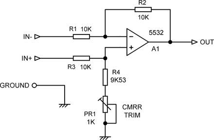
Figure 18.7 A balanced input amplifier, with preset pot to trim for best LF CMRR.
Figure 18.8 shows the CMRR measurements for a trimmed balanced input amplifier. The flat line at -50 dB was obtained from a standard fixed-resistor balanced input using four 1% 10 kΩ unselected resistors, while the much better (at LF, anyway) trace going down to -85 dB was obtained from Figure 18.7 by using a multi-turn preset for PR1. Note that R4 is an E96 value, so a 1k preset can swing the total resistance of that arm both above and below the nominal 10 kΩ. The CMRR is dramatically improved by more than 30 dB in the region 50–500 Hz, where ground noise tends to intrude itself, and is significantly better across almost all the audio spectrum.
The upward-sloping part of the trace in Figure 18.8 is partly due to the finite open-loop bandwidth of the opamp and partly due to unbalanced circuit capacitances. The CMRR is actually worse than 50 dB above 20 kHz due to the stray capacitances in the multi-turn preset. In practice, the value of PR1 would be smaller, and a one-turn preset with much less stray capacitance would be used. Still, I think you get the point; trimming can be both economic and effective.
Since the adjustment is somewhat critical, the amount of adjustment range should be limited to that necessary to cope with worst-case tolerance errors in all resistors, plus a safety margin.
Shock and vibration might affect preset adjustments in on-the-road mixing consoles. This can be prevented by using good-quality parts; multi-turn presets stay where they are put, but as noted, their stray capacitance can be a problem, and they are relatively expensive parts to apply to every line input. If a preset suffers failure it is usually the wiper losing contact with the track; it is wise to arrange the preset connections so that if this occurs, the CMRR will inevitably be degraded somewhat, but its basic function will continue. See Figure 18.7; if the preset wiper becomes disconnected, there is still a signal path through the preset track. If there was not, the CMRR would be destroyed and a significant gain error introduced.
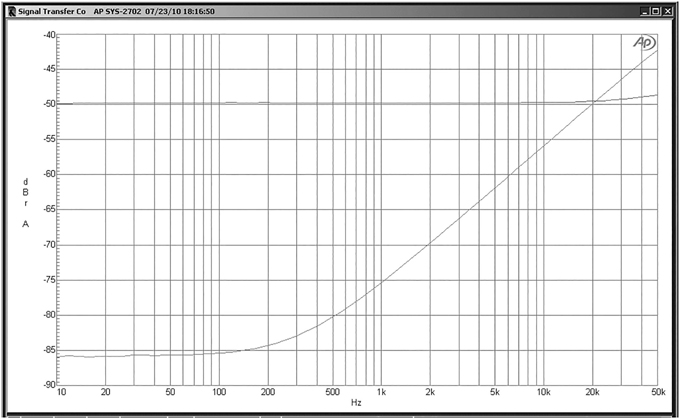
Figure 18.8 The CMRR of a fixed-resistor balanced amplifier compared with the trimmed version. The opamp was a 5532, and all resistors were 1%. The trimmed version gives better than 80 dB CMRR up to 500 Hz.
A Practical Balanced Input
The simple balanced input circuit shown in Figure 18.4 is not fit to face the outside world without additional components. Figure 18.9 shows a fully equipped version. First and most important, C1 has been added across the feedback resistor R2; this prevents stray capacitances from Pin 2 to ground causing extra phase shifts that lead to HF instability. The value required for stability is small, much less than that which would cause an HF roll-off anywhere near the top of the audio band. The values here of 10k and 27 pF give -3 dB at 589 kHz, and such a roll-off is only down by 0.005 dB at 20 kHz. C2, of equal value, must be added across R4 to maintain the balance of the amplifier, and hence its CMRR, at high frequencies.
C1 and C2 must not be relied upon for EMC immunity, as C1 is not connected to ground, and there is every chance that RF will demodulate at the opamp inputs. A passive RF filter is therefore added to each input, in the shape of R5, C3 and R6, C4, so the capacitors will shunt incoming RF to ground before it reaches the opamp. Put these as close to the input socket as possible to minimise radiation inside the enclosure.
I explained earlier in this chapter when looking at unbalanced inputs that it is not easy to guess what the maximum source impedance will be given the existence of “passive preamplifiers” and valve equipment. Neither is likely to have a balanced output unless implemented by transformer, but either might be used to feed a balanced input, and so the matter needs thought.
In the unbalanced input circuit, resistances had to be kept as low as practicable to minimise the generation of Johnson noise that would compromise the inherently low noise of the stage. The situation with a standard balanced input is, however, different from the unbalanced case, as there have to be resistances around the opamp, and they must be kept up to a certain value to give acceptably high input impedances; this is why a balanced input like this one is much noisier. We could therefore make R5 and R6 much larger without a measurable noise penalty if we reduce R1 and R3 accordingly to keep unity gain. In Figure 18.9, R5 and R6 are kept at 100 Ω, so if we assume 50 Ω output resistances in both legs of the source equipment, then we have a total of 150 Ω, and 150 Ω and 100 pF give -3 dB at 10.6 MHz. Returning to a possible passive preamplifier with a 10 kΩ potentiometer, its maximum output impedance of 2.5k plus 100 Ω with 100 pF gives -3 dB at 612 kHz, which remains well clear of the top of the audio band.
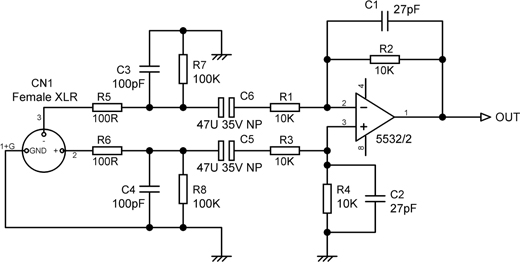
Figure 18.9 Balanced-input amplifier with the extra components required for DC blocking and EMC immunity.
As with the unbalanced input, replacing R5 and R6 with small inductors will give much better RF filtering but at increased cost. Ideally, a common-mode choke (two bifilar windings on a small toroidal core) should be used, as this improves performance. Check the frequency response to make sure the LC circuits are well damped and not peaking at the turnover frequency.
C5 and C6 are DC-blocking capacitors. They must be rated at no less than 35 V to protect the input circuitry and are the non-polarised type, as external voltages are of unpredictable polarity. The lowest input impedance that can occur with this circuit when using 10 kΩ resistors, is, as described earlier, 6.66 kΩ when it is being driven in the balanced mode. The low-frequency roll-off is therefore -3 dB at 0.51 Hz. This may appear to be undesirably low, but the important point is not the LF roll-off but the possible loss of CMRR at low frequencies due to imbalance in the values of C5 and C6; they are electrolytics with a significant tolerance. Therefore they should be made large so their impedance is a small part of the total input impedance. 47 μF is shown here, but 100 μF or 220 μF can be used to advantage if there is space to fit them in. The low-end frequency response must be defined somewhere in the input system, and the earlier the better, to prevent headroom or linearity being affected by subsonic disturbances, but this is not a good place to do it. A suitable time-constant immediately after the input amplifier is the way to go, but remember that capacitors used as time-constants may distort unless they are NP0 ceramic, polystyrene, or polypropylene. See Chapter 2 for more on this.
R7, R8 are DC drain resistors to prevent charges lingering on C5 and C6. These can be made lower than for the unbalanced input as the input impedances are lower, so a value of, say, 100 kΩ rather than 220 kΩ makes relatively little difference to the total input impedance.
A useful property of this kind of balanced amplifier is that it does not go mad when the inputs are left open circuit – in fact, it is actually less noisy than with its inputs shorted to ground. This is the opposite of the “normal” behaviour of a high-impedance unterminated input. This is because two things happen: open-circuiting the hot input doubles the resistance seen by the non-inverting input of the opamp, raising its noise contribution by 3 dB. However, opening the cold input makes the noise gain drop by 6 dB, giving a net drop in noise output of approximately 3 dB. This of course refers only to the internal noise of the amplifier stage, and pickup of external interference is always possible on an unterminated input. The input impedances here are modest, however, and the problem is less serious than you might think. Having said that, deliberately leaving inputs unterminated is always bad practice.
If this circuit is built with four 10 kΩ resistors and a 5532 opamp section, the noise output is -104.8 dBu with the inputs terminated to ground via 50 Ω resistors. As noted, the input impedance of the cold input is actually lower than the resistor connected to it when working balanced, and if it is desirable to raise this input impedance to 10 kΩ, it could be done by raising the four resistors to 16 kΩ; this slightly degrades the noise output to -103.5 dBu. Table 18.8 gives some examples of how the noise output depends on the resistor value; the third column gives the noise with the input unterminated and shows that in each case, the amplifier is about 3 dB quieter when open-circuited. It also shows that a useful improvement in noise performance is obtained by dropping the resistor values to the lowest that a 5532 can easily drive (the opamp has to drive the feedback resistor), though this usually gives unacceptably low input impedances. More on that at the end of the chapter.
| R value Ω | 50Ω terminated inputs | Open-circuit inputs | Terminated/open difference |
|---|---|---|---|
| 100k | –95.3 dBu | –97.8 dBu | 2.5 dBu |
| 10k | –104.8 dBu | –107.6 dBu | 2.8 dBu |
| 2k0 | –109.2 dBu | –112.0 dBu | 2.8 dBu |
| 820 | –111.7 dBu | –114.5 dBu | 2.8 dBu |
Variations on the Balanced Input Stage
I now give a collection of balanced input circuits that offer advantages or extra features over the standard balanced input configuration. The circuit diagrams often omit stabilising capacitors, input filters, and DC blocking capacitors to improve the clarity of the basic principle. They can easily be added; in particular, bear in mind that a stabilising capacitor like C1 in Figure 18.9 is often needed to guarantee freedom from high-frequency oscillation, and C2, of equal value, must also be added to maintain balance at HF.
Combined Unbalanced and Balanced Inputs
If both unbalanced and balanced inputs are required, it is extremely convenient if it can be arranged so that no switching between them is required. Switches cost money, mean more holes in the metalwork, and add to assembly time. Figure 18.10 shows an effective way to implement this. In balanced mode, the source is connected to the balanced input and the unbalanced input left unterminated. In unbalanced mode, the source is connected to the unbalanced input and the balanced input left unterminated, and no switching is required. It might appear that these unterminated inputs would pick up extra noise, but in practice, this is not the case. It works very well, and I have used it successfully in high-end equipment for two prestigious manufacturers.

Figure 18.10 Combined balanced and unbalanced input amplifier with no switching required.
As described, in the world of hi-fi, balanced signals are at twice the level of the equivalent unbalanced signals, and so the balanced input must have a gain of ½ or -6 dB relative to the unbalanced input to get the same gain by either path. This is done here by increasing R1 and R3 to 20 kΩ. The balanced gain can be greater or less than unity, but the gain via the unbalanced input is always approximately unity unless R5 is given a higher value to deliberately introduce attenuation in conjunction with R4.
There are two minor compromises in this circuit which need to be noted. First, the noise performance in unbalanced mode is worse than for the dedicated unbalanced input described earlier in this chapter, because R2 is effectively in the signal path and adds Johnson noise. Second, the input impedance of the unbalanced input cannot be very high because it is set by R4, and if this is increased in value, all the resistances must be increased proportionally, and the noise performance will be markedly worse. It is important that only one input cable should be connected at a time, because if an unterminated cable is left connected to an unused input, the cable capacitance to ground can cause frequency response anomalies and might, in adverse circumstances, cause HF oscillation. A prominent warning on the back panel and in the manual is a very good idea.
The Superbal Input
This version of the balanced input amplifier, shown in Figure 18.11, has been referred to as the “Superbal” circuit because it gives equal impedances into the two inputs for differential signals. It was publicised by David Birt of the BBC [6] but was apparently actually invented by M. Law and Ted Fletcher at Alice in 1978. Ted Fletcher discusses the issue on his website at [7], and apparently the original idea goes back to 1972. With the circuit values shown, the differential input impedance is exactly 10 kΩ via both hot and cold inputs. The common-mode input impedance is 20 kΩ as before.

In the standard balanced input R4 is connected to ground, but here its lower end is actively driven with an inverted version of the output signal, giving symmetry. The increased amount of negative feedback reduces the gain with four equal resistors to –6 dB instead of unity. The gain can be reduced below -6 dB by giving the inverter a gain of more than one; if R1, R2, R3, and R4 are all equal, the gain is 1/(A+1), where A is the gain of the inverter stage. This is of limited use, as the inverter U1:B will now clip before the forward amplifier U1:A, reducing headroom. If the gain of the inverter stage is gradually reduced from unity to zero, the stage slowly turns back into a standard balanced amplifier, with the gain increasing from -6 dB to unity and the input impedances becoming less and less equal. If a gain of less than unity is required, it should be obtained by increasing R1 and R3.
R5 and R6 should be kept as low in value as possible to minimise Johnson noise; there is no reason why they have to be equal in value to R1, etc. The only restriction is the ability of U1:A to drive R6 and U1:B to drive R5, both resistors being effectively grounded at one end. The capacitor C1 will almost certainly be needed to ensure HF stability; the value in the figure is only a suggestion. It should be kept as small as possible, because reducing the bandwidth of the inverter stage impairs CMRR at high frequencies.
Switched-Gain Balanced Inputs
A balanced input stage that can be switched to two different gains while maintaining CMRR is very useful. Equipment often has to give optimal performance with both semi-pro (-7.8 dBu) and professional (+4 dBu) input levels. If the nominal internal level of the system is in the normal range of -2 to -6 dBu, the input stage must be able to switch between amplifying and attenuating while maintaining good CMRR in both modes.
The brute-force way to change gain in a balanced input stage is to switch the values of either R1 and R3 or R2 and R4 in Figure 18.4, keeping the pairs equal in value to maintain the CMRR; this needs a double-pole switch for each input channel. A much more elegant technique is shown in Figure 18.12. Perhaps surprisingly, the gain of a differential amplifier can be manipulated by changing the drive to the feedback arm (R2 etc.) only and leaving the other arm R4 unchanged, without affecting the CMRR. The essential point is to keep the source resistance of the feedback arm the same but drive it from a scaled version of the opamp output. Figure 18.12 does this with the network R5, R6, which has a source resistance made up of 6k8 in parallel with 2k2, which is 1.662 kΩ. This is true whether R6 is switched to the opamp output (low gain setting) or to ground (high gain setting), for both have effectively zero impedance. For low gain, the negative feedback is not attenuated but fed through to R2 and R7 via R5, R6 in parallel. For high gain R5 and R6 become a potential divider, so the amount of feedback is decreased and the gain increased. The value of R2 + R7 is reduced from 7k5 by 1.662 kΩ to allow for the source impedance of the R5, R6 network; this requires the distinctly non-standard value of 5.838 kΩ, which is here approximated by R2 and R7 which give 5.6 kΩ + 240Ω = 5.840 kΩ. This value is the best that can be done with E24 resistors; it is obviously out by 2 Ω, but that is much less than a 1% tolerance on R2 and so will have only a vanishingly small effect on the CMRR.

Figure 18.12 A balanced input amplifier with gain switching that maintains good CMRR.
Note that this stage can attenuate as well as amplify if R1, R3 are set to be greater than R2, R4, as shown here. The nominal output level of the stage is assumed to be -2 dBu; with the values shown, the two gains are -6.0 and +6.2 dB, so +4 dBu and -7.8 dBu respectively will give -2 dBu at the output. Other pairs of gains can of course be obtained by changing the resistor values; the important thing is to stick to the principle that the value of R2 + R7 is reduced from the value of R4 by the source impedance of the R5, R6 network. With the values shown, the differential input impedance is 11.25 kΩ via the cold and 22.5 kΩ via the hot input. The common-mode input impedance is 22.5 kΩ.
This neat little circuit has the added advantage that nothing bad happens when the switch is moved with the circuit operating. When the wiper is between contacts, you simply get a gain intermediate between the high and low settings, which is pretty much the ideal situation.
Variable-Gain Balanced Inputs
The beauty of a variable-gain balanced input is that it allows you to get the incoming signal up or down to the nominal internal level as soon as possible, minimising both the risk of clipping and contamination with circuit noise. The obvious method of making a variable-gain differential stage is to use dual-gang pots to vary R2, R4 together to maintain CMRR. (Varying R1, R3 would also alter the input impedances.) This is clumsy and gives a CMRR that is both bad and highly variable due to the inevitable mismatches between pot sections. For a stereo input, the required four-gang pot is an unappealing proposition.
There is, however, a way to get a variable gain with good CMRR, using a single pot section. The principle is essentially the same as for the switched-gain amplifier: keep constant the source impedance driving the feedback arm but vary the voltage applied. The principle is shown in Figure 18.13. To the best of my knowledge, I invented this circuit in 1982; any comments on this point are welcome. The feedback arm R2 is driven by voltage-follower U1:B. This eliminates the variations in source impedance at the pot wiper, which would badly degrade the CMRR. R6 sets the maximum gain, and R5 modifies the gain law to give it a more usable shape. The minimum gain is set by the R2/R1 ratio. When the pot is fully up (minimum gain), R5 is directly across the output of U1:A, so do not make it too low in value. If a centre-detent pot is used to give a default gain setting, this may not be very accurate, as it partly depends on the ratio of pot track (no better than ±20% tolerance and sometimes worse) to 1% fixed resistors.
This configuration is very useful as a general line input with an input sensitivity range of -20 to +10 dBu. For a nominal output of 0 dBu, the gain of Figure 18.13 is therefore +20 to -10 dB, with R5 chosen to give 0 dB gain at the central wiper position. An opamp in a feedback path may appear a dubious proposition for HF stability because of the extra phase shift it introduces, but here it is working as a voltage-follower, so its bandwidth is maximised, and in practice, the circuit is dependably stable.

Figure 18.13 Variable-gain balanced input amplifier: gain +20 to -10 dB.
This configuration can be improved. The maximum gain in Figure 18.13 is set by the end stop resistor R6 at the bottom of the pot. The pot track resistance will probably be specified at ±20%, while the resistor will be a much more precise 1%. The variation of pot track resistance can therefore cause quite significant differences between the two channels. It would be nice to find a way to eliminate this, in the same way that the Baxandall volume control eliminates any dependency on the pot track. We could do this if we could get rid of the law-bending resistor R5 and also lose the end stop resistor R6; the pot would then be working as a pure potentiometer, with its division ratio controlled by the angular position of the wiper alone. If the gain range is restricted to around 10 dB, there is no very pressing need for law-bending, and R5 can be simply omitted. However, if we simply do away with the end stop resistor R6, the gain is going to be uncontrollably large with the pot wiper at the bottom of its track. We need a way to limit the maximum gain that keeps other resistors away from the pot.
The noise outputs at various gains are given in Table 18.9. The inputs were terminated with 47 Ω resistors to ground.
Combined Line Input and Balance Control Stage With Low Noise
This is a balanced low-noise input stage with gain variable over a limited range to implement the stereo balance control function. Maximum gain is +3.7 dB and minimum gain –6.1 dB, which may not sound like much but is more than enough for effective stereo balance control. Gain with balance central is +0.2 dB, which I would suggest is close enough to unity for anyone.
The noise of the stage is reduced by low-impedance design. Compared with Figure 8.13, the input resistors R7, R8 have been reduced from 15 kΩ to 1 kΩ and the feedback and attenuation arms to 500 Ω. This requires the addition of input buffers to give a reasonably high input impedance; in this case, it is set to 50 kΩ but could easily be made higher. The schematic in Figure 8.14 shows the stage fully equipped to meet the real world with EMC filtering R1, C1 and R2, C2 and non-polar DC blocking capacitors C3, C4. R3, R4 are the DC drain resistors.
| Max gain | Unity gain | Min gain | |
|---|---|---|---|
| 5532 | –99.7 dBu | –103.4 dBu | –109.3 dBu |
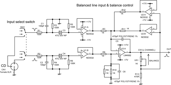
Figure 18.14 Variable-gain balanced-input amplifier. Gain here is +3.7 to -6.1 dB, with unity gain for control central.
U3:A is the basic balanced amplifier; it is an LM4562 for low-voltage noise and good driving ability. The stage gain and its range is set by 1 kΩ pot VR1 and R13. The negative feedback to U3:A is applied through two parallel unity-gain buffers U2:A and U2:B, so the variation in output impedance of the gain-control network will not degrade the CMRR.
The dual buffers reduce noise by partial cancellation of their own voltage noise and give also more drive capability so the feedback resistors can be low. In this stage, combining the buffer outputs is simple, with no need for 10 Ω resistors, because the feedback resistance can be conveniently split into R11 and R12. The attenuation arm is then made up of two 1 kΩ resistors R9, R10 in parallel to exactly match R11, R12 and so give good CMRR. Resist the cheapskate temptation to use a single 470 Ω instead, because that would degrade the CMRR significantly. The measured noise results are given in Table 18.10, with the inputs terminated with 47 Ω resistors to ground and with RMS-subtraction of the test gear noise floor. The top row shows the results with a 5532 for the basic balanced amplifier and only one buffer driving a 50 Ω feedback resistor. The middle row shows the relatively modest noise reduction achieved by using twin buffers and two 1 kΩ feedback resistors; this looks at first sight hardly worth it but is essential if we want the full improvement given by springing the money for an LM4562 as U3:A. The bottom row shows the final result and is, I think all will agree, rather quiet.
This input/balance stage, with the twin buffers and the LM4562, was used in my Elektor 2012 preamp design, where all the pots were 1 kΩ for low noise. [8] It was designed before I had the insight on pot-dependence described in the next section. Concerned about the effect of the pot value tolerances, I measured a number of the pots used, which had a nominal ±20% tolerance, and found the extreme values to be +5% and -7.8%. These led to worst-case gain errors of less than 0.1 dB, so I decided the problem was under control.
The Self Variable-Gain Line Input
I was just going to bed at dawn (the exigencies of the audio service, ma’am) when it occurred to me that the answer is to add a resistor that gives a separate feedback path around the differential opamp U1:A only. R7 in Figure 18.15 provides negative feedback independently of the gain control and so limits the maximum gain. It is not intuitively obvious (to me, at any rate), but the CMRR is still completely preserved when the gain is altered, just as for Figure 18.13. You will note in Figure 18.15 that two resistors R4, R8 are paralleled to get a value exactly equal to R2 in parallel with R7. It shows resistor values that give a gain range suitable for combining an active stereo balance control with a balanced line input in one economical stage. The minimum gain is -3.3 dB and the maximum gain of +6.6 dB. The gain with the pot wiper central is +0.2 dB, which once more I suggest is close enough to unity for most of us. This concept eliminates the effect of pot track resistance on gain, and I propose to call it the Self Input. All right?
| Max gain | Unity gain | Min gain | |
|---|---|---|---|
| 5532 1xFB buffer | –103.4 dBu | –107.0 dBu | –113.3 dBu |
| 5532 2xFB buffer | –104.0 dBu | –107.6 dBu | –113.9 dBu |
| LM4562 2xFB buffer | –105.9 dBu | –109.4 dBu | –115.7 dBu |

The gain equation looks more complex than for the previous example, but it is actually just a slight elaboration. The gain is now controlled by the ratio of R1 (=R3) to the parallel combination of R7 and R2, the latter being effectively scaled by the factor A introduced by the pot setting.
The Self Input stage in Figure 18.15 has reasonably high resistor values to allow direct connection to outside circuitry. As for the other configurations in this chapter, the noise performance can be much improved by scaling down all the resistor values and driving the inputs via a pair of unity-gain buffers; the low-value resistors reduce Johnson noise and the effect of opamp input current noise flowing through them; in this form, it was used in my recent Linear Audio preamp design.[9] There is much more on reducing noise in this way later in this chapter.
High Input-Impedance Balanced Inputs
We saw earlier that high input impedances are required to maximise the CMRR of a balanced interconnection, but the input impedances offered by the standard balanced circuit are limited by the need to keep the resistor values down to control Johnson noise and the effects of current noise. High-impedance balanced inputs are also useful for interfacing to valve equipment in the strange world of retro hi-fi. Adding output cathode-followers to valve circuitry is expensive and consumes a lot of extra power, and so the output is often taken directly from the anode of a gain-stage, and even a so-called bridging load of 10 kΩ may seriously compromise the distortion performance and output capability of the source equipment.
Figure 18.16 shows a configuration in which the input impedances are determined only by the bias resistances R1 and R2. They are shown here as 100 kΩ, but they may be considerably higher if opamp bias currents permit. A useful property of this circuit is that adding a single resistor Rg increases the gain but preserves the circuit balance and CMRR. This configuration cannot be set to attenuate because the gain of an opamp with series feedback cannot be reduced below unity.
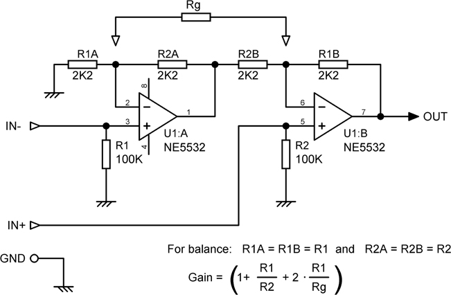
It is of course always possible to give a basic balanced input a high input impedance by putting unity-gain buffers in front of each input, but that uses three opamp sections rather than two. Sometimes, however, it is appropriate. Much more on that later.
We noted earlier that the simple balanced input is surprisingly quiet and well behaved when its inputs are unterminated. This is not the case with this configuration, which, because of its high input impedances, will be both noisy and susceptible to picking-up external interference.
The Inverting Two-Opamp Input
The configuration depicted in Figure 18.17 has its uses because the hot and cold inputs have the same impedances for differential signals, as well as for common-mode voltages.[10] It is not suited to high input impedances at normal gains because high resistor values would have to be used throughout, and they would generate excess Johnson noise, but if it is interfacing with a high-voltage source so the gain must be well below unity, R1 and R3 can be made high in value, and R2, R4, R5 set low, the latter components keeping the noise down. The CMRR may degrade at HF because the hot signal has gone through an extra opamp and suffered phase shift, interfering with the subtraction; this can be compensated for by the network Rc-1, Rc-2, and C1; the values needed depend on opamp type and must be checked by CMRR measurements.
I have used this configuration for balanced input feeds from a 100 V loudspeaker line of the sort still in use for distributing audio over wide areas. The circuit values shown reduce the 100 V input to a nominal -2 dBu (615 mV) internal level. If this circuit is used for that purpose, then effective input overvoltage protection on the inputs is essential as large voltage transients are possible on a loudspeaker line if parts of it are unplugged or plugged with signal present due to the inductance of the line matching transformers. This protection can be conveniently provided by the usual diode clamps to the supply rails; this is dealt with at the end of this chapter. The input resistors will be of high value in this application, so there is very little possibility of excessive inputs overheating the resistors or “pumping up” the opamp supply rails.
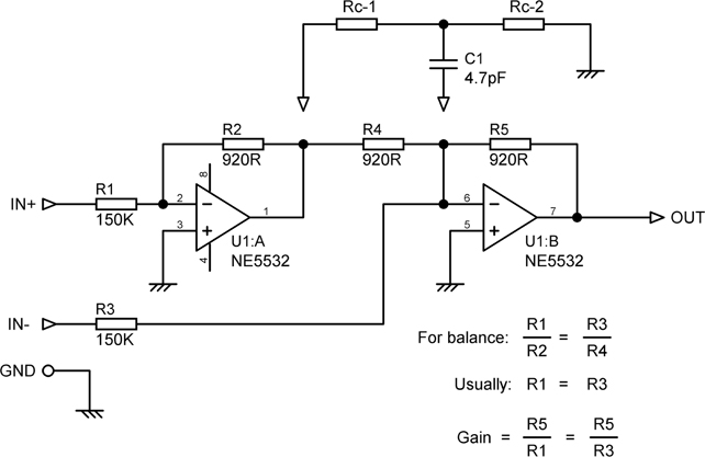
The Instrumentation Amplifier
Almost every book on balanced or differential inputs includes the three-opamp circuit of Figure 18.18 and praises it as the highest expression of the differential amplifier. It is usually called the instrumentation amplifier configuration because of its undoubted superiority for data acquisition. (Specialised ICs exist that are sometimes also called instrumentation amplifiers or in-amps; these are designed for very high CMRR data acquisition. They are expensive and in general not optimised for audio work.)
The dual input stage U1:A, U1:B buffers the balanced line from the input impedances of the final differential amplifier U2:A, so the four resistances around the latter can be made much lower in value, reducing their Johnson noise and the effects of opamp current noise by a significant amount while keeping the CMRR benefits of presenting high input impedances to the balanced line. However, the true beauty of the instrumentation amplifier, much emphasised because of its unquestionable elegance, is that the dual input stage, with its shared feedback network R3, R4, R5, can be set to have a high differential gain by giving R4 a low value, but its common-mode gain is always unity; this property is not affected by mismatches in R3 and R5. The final amplifier then does its usual job of common-mode rejection, and the combined CMRR can be very good indeed (over 100 dB) if the first-stage gain is high.
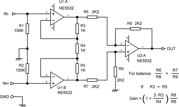
Figure 18.18 The instrumentation amplifier configuration. Gain here is 3 times.
This is all well and good, but it is not immediately obvious that the instrumentation amplifier configuration can usefully improve the CMRR of audio balanced line inputs. A data-acquisition application like ECG monitoring may need a gain of thousands of times; a good portion of this will be put into the first stage, allowing a stunning CMRR to be achieved without using precision resistors. Unfortunately, the cruel fact is that in audio usage, this much gain at a line input this point is simply not wanted except for microphone amplifiers. In a typical signal path comprised of opamps, the nominal internal level is usually between -6 and 0 dBu, and the line level coming in is at the professional level of +4 dBu; what is needed is 6 dB of attenuation rather than any gain. Gain at this point and attenuation later would introduce what can only be described as a headroom bottleneck. If the incoming level was the semi-pro -7.8 dBu, a small amount of gain could be introduced.
So does this mean that the instrumentation amplifier configuration has no real advantages over an ordinary balanced amplifier with input buffers? No. Stand by for what I believe is a whole new way of looking at this stage.
Instrumentation Amplifier Applications
First, there are some applications where gain in a balanced input amplifier is either essential or can be made use of. Active crossovers and power amplifiers are probably the two most common.
Active crossovers are commonly used with no volume control or only a limited-range gain trim between them and the power amplifiers, so that it can always be assumed that the power amplifier will clip first. As I pointed out in [11], under these conditions, the crossover can be run at an internal level of 3 Vrms or more, with the output level dropped back to, say, 1 Vrms at the very output of the crossover by a low-impedance passive attenuator. This can give a very impressive noise performance because the signal goes through the chain of filters at a high level. [12]
For a typical active crossover application like this, we therefore need an input stage with gain. If the nominal input is 0 dBu (775 mVrms), we want a gain of about 4 times to get the signal up to 3 Vrms (+11.8 dBu). We will not need a greater output than this because it is sufficient to clip the following power amplifiers, even after the passive attenuators. This demonstrates that you can break The Rule “Do not amplify then attenuate” so long as there is a more severe headroom restriction downstream and a limited gain control range.
If we use the strategy of input buffers followed by balanced amplifiers working at low impedances, as described later in this chapter (i.e. not an instrumentation amplifier, as there is no network between the two input opamps), the required gain can be obtained by altering the ratio of the resistors in the balanced amplifier of a 1–1 configuration. With suitable resistor values (R1 = R3 =560R, R2 = R4 = 2k2), the output noise from this stage (inputs terminated by 50 Ω) is -100.9 dBu, so its equivalent input noise (EIN) is -100.9−11.8 = -112.7 dBu, which is reasonably quiet. All noise measurements are 22–22kHz, rms sensing, unweighted, and 5532 opamps are used.
The other area for instrumentation amplifier techniques is that of power amplifiers with balanced inputs. The voltage gain of the power amplifier itself is frequently about 22 times (+26.8 dB) for its own technical reasons. If we take a power output of 100W into 8Ω as an example, the maximum output voltage is 28.3 Vrms, so the input level must be 28.3/22 = 1.29 Vrms. If the nominal input level is +4 dBu (1.23 Vrms), then a very modest gain of 1.05 times is required, and we will gain little from using an instrumentation amplifier with that gain in Stage 1. If, however, the nominal input level is 0 dBu (0.775 Vrms), a higher gain of 1.66 times is needed, but that is still only a theoretical CMRR improvement of 4.4 dB. However, we can again make use of the fact that a relatively small signal voltage is enough to clip the power amplifier, and we can amplify the input signal –perhaps by 4 times again –and then attenuate it, along with the noise from the balanced input amplifier.
The Instrumentation Amplifier With 4x Gain
Since we need a significant amount of gain, the instrumentation amplifier configuration is a viable alternative to the input buffer-balanced amplifier approach, giving a CMRR theoretically improved by 11.8 dB, the gain of its first stage. It uses the same number of opamps –three. A suitable circuit is shown in Figure 18.19. This gives a gain of 3.94 times, which is as close as you can get to 4.00 with single E24 values. My tests show that the theoretical CMRR improvement really is obtained. To take just one set of results, when I built the second stage, it gave a CMRR of -56 dB working alone, but when the first stage was added, the CMRR leapt up to -69 dB, an improvement of 13 dB. These one-off figures (13 dB is actually better than the 12 dB improvement you would get if all resistors were exact) obviously depend on the specific resistor examples I used, but you get the general idea. The CMRR was flat across the audio band.
I do realise that there is an unsettling flavour of something for nothing about this, but it really does work. The total gain required can be distributed between the two stages in any way, but it should all be concentrated in Stage 1, as shown in Figure 18.19, to obtain the maximum CMRR benefit.

Figure 18.19 Instrumentation-amplifier balanced input stage with gain of 4 times.
What about the noise performance? Fascinatingly, it is considerably improved. The noise output of this configuration is usefully lower at -105.4 dBu, which is no less than 4.5 dB better than the -100.9 dBu we got from the more conventional 1–1 configuration described earlier. This is because the amplifiers in Stage 1 are working in better conditions for low noise than those in Stage 2. They have no significant resistance in series with the non-inverting inputs to generate Johnson noise or turn the opamp current noise into voltage noise. As they implement all the gain before the signal reaches Stage 2, the noise contribution of the latter is therefore less significant.
When noise at –105.4 dBu is put through a 10 dB passive attenuator to get back down to the output level we want, as might typically be done at the output of an active crossover, it will become -115.4 dBu, which I suggest is very quiet indeed.
The circuit in Figure 18.19 requires some ancillary components before it is ready to face the world. Figure 18.20 shows it with EMC RF filtering (R19, C1 and R20, C4) non-polarised DC-blocking capacitors (C2, C3), and capacitors C5, C6 to ensure HF stability. R21, R22 are DC-drain resistors that ensure that any charge left on the DC-blocking capacitors by the source equipment when the connector is unplugged is quickly drained away. These extra components are omitted from subsequent diagrams to aid clarity.
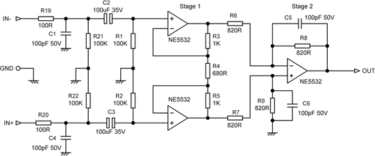
Figure 18.20 Practical instrumentation-amplifier balanced input stage with gain of 4 times.
So here we are with all of the gain in the first stage, for the best CMRR, and this is followed by a unity-gain Stage 2. Now let’s extend this thinking a little. Suppose Stage 2 had again of less than unity? We could then put more gain in Stage 1 and get a further free and guaranteed CMRR improvement while keeping the overall gain the same. But can we do this without causing headroom problems in Stage 1?
The instrumentation amplifier in Figure 18.21 has had the gain of Stage 1 doubled to 8 times (actually 7.67 times; 0.36 dB low, but as close as you can get with single E24 values) by reducing R4, while the input resistors R6, R7 to Stage 2 have been doubled in value so that stage now has a gain of 0.5 times, to keep the total gain at approximately 4 times.
In this case, the theoretical CMRR improvement is once more the gain of Stage 1, which is 7.67 times, and therefore 17.7 dB. Stage 2 gave a measured CMRR of -53 dB working alone, but when Stage 1 was added the CMRR increased to -70 dB, an improvement of 17 dB, significantly greater than the 14 dB improvement obtained when Stage 1 had a gain of 4 times. The noise output was –106.2 dBu, which is better than the four-times instrumentation amplifier by 0.8 dB and better than the somewhat more conventional 1–1 configuration by a convincing 5.3 dB. When the noise level of –106.2 dBu is put through the 10 dB passive attenuator to get back down to the level we want, this will become -116.2 dBu, which is even quieter than the previous version.
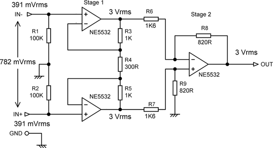
You may well be getting nervous about having a gain as high as 8 times followed by attenuation; have we compromised the headroom? If we assume that, as before, the maximum output we need is 3 Vrms, then with a total gain of 4 times, we will have 0.775 Vrms between the two inputs, and the corresponding signal voltages at each output of Stage 1 are also 3 Vrms. These outputs are in anti-phase, and so when they are combined in Stage 2, with its gain of 0.5 times, we get 3 Vrms at the final output. This means that in balanced operation, all three amplifiers will clip simultaneously, and the input amplifier can pass the maximum opamp output level before clipping. With the usual ±17 V supply rails, this is about 10 Vrms.
So far so good; all the voltages are well below clipping. But note that we have assumed a balanced input, and unless you are designing an entire system, that is a dangerous assumption. If the input is driven with an unbalanced output of the same level, we will have 0.775 Vrms on one input pin and nothing on the other. You might fear we would get 6 Vrms on one output of Stage 1 and nothing on the other; that would still be some way below clipping, but the safety margin is shrinking fast. In fact, things are rather better than that. The cross-coupling of the feedback network R3, R4, R5 greatly reduces the difference between the two outputs of stage 1 with unbalanced inputs. With 0.775 Vrms on one input pin and nothing on the other, the Stage 1 outputs are 3.39 Vrms and 2.61 Vrms, which naturally sum to 6 Vrms, reduced to 3 Vrms out by Stage 2. The higher voltage is at the output of the amplifier associated with the driven input. Maximum output with an unbalanced input is slightly reduced from 10 Vrms to 9.4 Vrms. This minor restriction does not apply to the earlier version with only 4 times gain in Stage 1.
This shows us that if we can assume a balanced input and stick with a requirement for a maximum output of 3 Vrms, we have a bit more elbowroom than you might think for using higher gains in Stage 1 of an instrumentation amplifier. Taking into account the possibility of an unbalanced input, we could further increase the gain by a factor of 10/3.39 = 2.95 times, on top of the doubling of Stage 1 gain we have already implemented. This gives a Stage 1 gain of 22.6 times. I decided to be conservative and go for a Stage 1 gain of 21 times; the gain of Stage 2 is correspondingly reduced to 0.19 times to maintain a total gain of 4 times. This version is shown in Figure 18.22; you will note that the feedback resistors R3, R4, R5 in Stage 1 have been scaled up by a factor of two. This is because Stage 1 is now working at a higher level; remember also that the resistors R3 and R5 are not the only load on Stage 1, because each of its opamp outputs is looking at the Stage 2 inputs driven in anti-phase, so its inverting input loading is heavier than it at first appears; see the section on The Basic Electronic Balanced Input for an explanation of why the inverting input of Stage 2 presents a lower impedance than is apparent. Leaving R3, R5 at 1kΩ would significantly degrade the distortion performance; I found it increased the THD at 10 kHz from 0.0012% to 0.0019% for a 3 Vrms output.
When Stage 2 was tested alone, its CMRR was -61 dB; clearly we have been lucky with our resistors. Adding on Stage 1 increased it to a rather spectacular -86 dB, an improvement of no less than 25 dB. This degrades to -83 dB at 20 kHz; this is the first time it has not appeared flat across the audio band. The theoretical CMRR improvement is 26.4 dB, without trim presets or selected components.
The output noise level remains at –106.2 dBu; we have clearly gained all the noise advantage we can by increasing the Stage 1 gain.
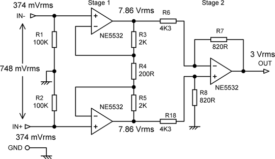
Note that throughout this discussion, I have assumed that there are no objections to running an opamp at a signal level not far from clipping and in particular that the distortion performance is not significantly harmed by doing that. This is true for many modern opamps such as the LM4562 and also for the veteran 5532 when it is not loaded to the limit of its capability.
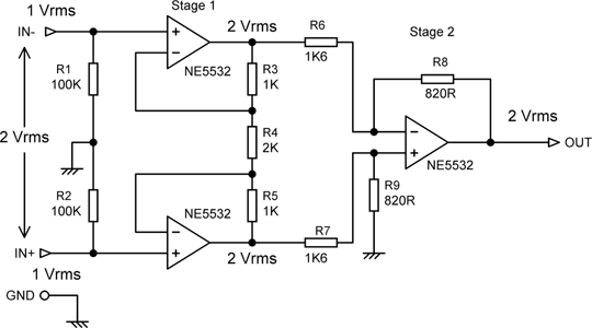
Figure 18.23 Instrumentation-amplifier balanced input stage with gain of 2 times in Stage 1 and 0.5 times in Stage 2 for overall unity gain.
The Instrumentation Amplifier at Unity Gain
If you want a unity-gain input stage but also some CMRR improvement, some compromise is required.
Putting R3, R5 = 1kΩ and R4 = 2kΩ gives a Stage 1 gain of 2 times, which is undone by setting R6, R7 to 1k6 in Stage 2 to give a gain of 0.5 times. This will pass the full 10 Vrms maximum opamp level but only in balanced mode. In unbalanced mode Stage 1 will clip at the opamp connected to the driven input, because when unbalanced, the gain to this point from the input is 1.5 times. The maximum signal that can be handled in unbalanced mode is therefore about 7 Vrms. The resulting input amplifier is shown in Figure 18.23. A heavy load is placed on the Stage 1 amplifiers in this situation, and for the best distortion behaviour, it would be better to make R3, R5 = 2kΩ and R4 = 4kΩ.
When I did the measurements, Stage 2 alone had a CMRR of -57 dB; adding on Stage 1 brought this up to -63 dB. (This exact correspondence of theoretical and measured improvement is just a coincidence.) You can therefore have 6 dB more CMRR free, gratis, and for absolutely nothing, so long as you are prepared to tolerate a loss of 3.5 dB in headroom if the stage is run unbalanced but with the same input voltage. The noise output is -111.6 dBu.
The Instrumentation Amplifier and Gain Controls
A typical hi-fi output gives 1 Vrms in unbalanced use and 2 Vrms when run balanced, as the cold output is provided by a simple inverter, the presence of which doubles the total output voltage. Figure 18.24 shows the signal voltages when our unity-gain input stage is connected to a 2 Vrms balanced input. This sort of situation is more likely to occur in hi-fi than in professional audio; in the latter, simulated “floating transformer winding” outputs are sometimes found, where the total output voltage is the same whether the output is run balanced or unbalanced. These are described in Chapter 19.
In hi-fi use, it may be possible to assume that the instrumentation amplifier will never be connected to a balanced output with a total signal voltage of more than 2 Vrms. If this is the case, we can once more put extra gain into Stage 1 and undo it with stage 2 without compromising headroom. We are now dealing with a restriction on input level rather than output level. We will assume that the 2 Vrms input is required to be reduced to 1 Vrms to give adequate headroom in the circuitry that follows, so an overall gain of 0.5 times is required.

Finally, we will look at how the range of gain control between the instrumentation amplifier and the power amplifier affects the headroom situation. Figure 18.24 shows one of the instrumentation amplifiers described earlier with a maximum output of 3 Vrms, the version in Figure 18.21 with a gain of 8 times in Stage 1 and 0.5 times in Stage 2. This is followed by a ±10 dB gain trim network that is normally expected to work at the 0 dB setting, i.e. giving 10 dB of attenuation and so reducing the noise from the input stage. I should point out that with a linear pot, this simple network does not give “0 dB” at the centre of the pot rotation; that point is more like three-quarters of the way down.
Since the maximum output of this stage is 10 Vrms with a balanced input (slightly less with an unbalanced input), clipping will always occur in the power amplifier first so long as the gain trim is set above -10 dB. At the -10 dB setting (which introduces 20 dB of actual attenuation), the input amplifier and the power amp will clip simultaneously; if more attenuation is permitted, then there is the danger that the input amplifier will clip first, and this cannot be corrected by the gain trim. Note the low resistor values in the gain trim network to minimise Johnson noise and also the effect of the power amplifier input noise current. A low source impedance is also required by most power amplifiers to prevent input current distortion. [13] In the worst-case position (approximately wiper central), the output impedance of the network is 275 Ω, and the Johnson noise from that resistance is -128.2 dBu, well below the noise from the input amplifier, which is -106.2 dBu–6 dB = -112.2 dBu, and also below the equivalent input noise of the power amplifier, which is unlikely to be better than -122 dBu.
The Instrumentation Amplifier and the Whitlock Bootstrap
In some balanced applications, the hot and cold source resistances may not be exactly the same. In a typical balanced link, the output resistors of the sending equipment are likely to be in the range 47 Ω–100 Ω and of 1% tolerance, and when used with the 100 kΩ input bias resistors shown, the effect is likely to be negligible. However, if the source impedances are higher, it is important to keep the common-mode impedance as high as possible to maximise the CMRR. It is going to be difficult to increase the input bias resistors without creating excessive DC offsets, but there is a very clever way of bootstrapping them, introduced by Bill Whitlock in an AES paper in 1996. [14]
As noted, the common-mode gain of the first stage of an instrumentation amplifier is always unity, no matter what differential gain is set by R3, R4, R5, so a common-mode bootstrapping signal can be derived by the two resistors R10, R11. The unity-gain buffer A4 then uses this to drive the midpoint of R1–R2, raising the common-mode impedance considerably. Figure 18.25 shows the unity-gain instrumentation amplifier of Figure 18.19 with bootstrapping added; the component values are mine. R12 provides a DC path for biasing the opamps. Since C1 is not in the differential signal path, with the circuit as shown, the frequency response extends down to DC; in practice, input DC-blocking capacitors would be used.
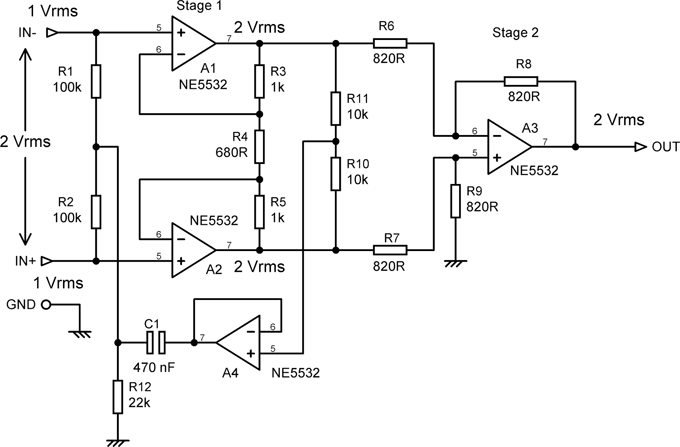
The Whitlock bootstrap is used in the THAT 1200 line receiver IC. EDN tested it and some of its competitors, and you can read about it here. [15] Note that the Whitlock bootstrap is the subject of a US patent [16], and if you plan to use it commercially, you had better talk to THAT Corporation about licensing.
Transformer Balanced Inputs
When it is essential that there is no galvanic connection (i.e. no electrical conductor) between two pieces of equipment, transformer inputs are indispensable. They are also useful if EMC conditions are severe. Figure 18.26 shows a typical transformer input. The transformer usually has a 1:1 ratio and is enclosed in a metal shielding can, which must be grounded. Good line transformers have an inter-winding shield that must also be grounded, or the high-frequency CMRR will be severely compromised. The transformer secondary must see a high impedance, as this is reflected to the primary and represents the input impedance; here it is set by R2, and a buffer drives the circuitry downstream. In addition, if the secondary loading is too heavy, there will be increased transformer distortion at low frequencies. Line input transformers are built with small cores and are only intended to deliver very small amounts of power; they are not interchangeable with line output transformers. A most ingenious approach to dealing with this distortion problem by operating the input transformer core at near-zero flux was published by Paul Zwicky in 1986 [17]
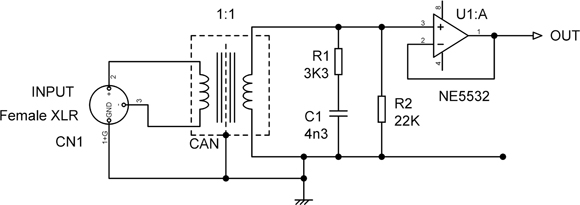
There is a bit more to correctly loading the transformer secondary. If it is simply loaded with a high-value resistor, there will be peaking of the frequency response due to resonance between the transformer leakage inductance and the winding capacitance. This is shown in Figure 18.27, where a Sowter 3276 line input transformer (a high-quality component) was given a basic resistive loading of 100 kΩ. The result was Trace A, which has a 10 dB peak around 60 kHz. This is bad not only because it accentuates the effect of out-of-band noise but because it intrudes on the audio frequency response, giving a lift of 1 dB at 20 kHz. Reducing the resistive load R2 would damp the resonance, but it would also reduce the input impedance. The answer is to add a Zobel network, i.e. a resistor and capacitor in series, across the secondary; this has no effect except high frequencies. The first attempt used R1 = 2k7 and C1= 1 nF, giving Trace B, where the peaking has been reduced to 4 dB around 40 kHz, but the 20 kHz lift is actually slightly greater. R1 = 2k7 and C1= 2 nF gave Trace C, which is a bit better in that it only has a 2 dB peak. Some more experimentation resulted in R1 = 3k3 and C1= 4.3 nF (3n3 + 1nF) and yielded Trace D, which is pretty flat, though there is a small droop around 10 kHz. The Zobel values are fairly critical for the flattest possible response and must certainly be adjusted if the transformer type is changed.
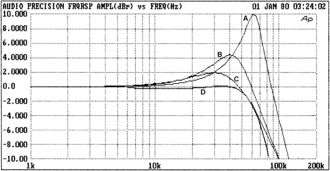
Figure 18.27 Optimising the frequency response of a transformer balanced input with a Zobel network.
Input Overvoltage Protection
Input overvoltage protection is not common in hi-fi applications but is regarded as essential in most professional equipment. The normal method is to use clamping diodes, as shown in Figure 18.26, that prevent certain points in the input circuitry from moving outside the supply rails.
This is straightforward, but there are two points to watch. First, the ability of this circuit to withstand excessive input levels is not without limit. Sustained over voltages may burn out R5 and R6 or pump unwanted amounts of current into the supply rails; this sort of protection is mainly aimed at transients. Second, diodes have a non-linear junction capacitance when they are reverse biased, so if the source impedance is significant, the diodes will cause distortion at high frequencies. To quantify this problem, here are the results of a few tests. If Figure 18.28 is fed from the low impedance of the usual kind of line output stage, the impedance at the diodes will be about 1 kΩ, and the distortion induced into an 11 Vrms 20 kHz input will be below the noise floor. However, if the source impedance is high so the impedance at the diodes is increased to 10 kΩ, with the same input level, the THD at 20 kHz was degraded from 0.0030% to 0.0044% by adding the diodes. I have thought up a rather elegant way to eliminate this effect completely; anybody interested?
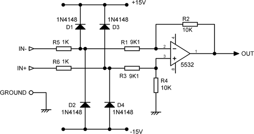
Figure 18.28 Input overvoltage protection for a balanced input amplifier.
Low-Noise Balanced Inputs
So far, we have not said much about the noise performance of balanced inputs, though we have noted several times that the standard balanced input amplifier with four 10 kΩ resistors as in Figure 18.29a is markedly noisier than an unbalanced input like that in Figure 18.1. The unbalanced input stage, with its input terminated by 50 Ω to ground, has a noise output of -119.0 dBu over the usual 22–22 kHz bandwidth. If the balanced circuit is built with 10 kΩ resistors and a 5532 section, the noise output is -104.8 dBu with the inputs similarly terminated. This is a big difference of 14.2 dB.
In the hi-fi world in particular, where an amplifier may have both unbalanced and balanced inputs, many people would feel that this situation is the wrong way round. Surely the balanced input, with its professional XLR connector and its much-vaunted rejection of ground noise, should show a better performance in all departments? Well, it does –except as regards internal noise, and a 14 dB discrepancy is both clearly audible and hard to explain away. This section explains how to design it away instead.
We know that the source of the extra noise is the relatively high resistor values around the opamp (see Table 18.8 earlier in the chapter), but these cannot be reduced in the simple balanced stage without reducing the input impedances below what is acceptable. The answer is to lower the resistor values but buffer them from the input with a pair of voltage-followers; this arrangement is shown in Figure 18.29b. 5532s are a good choice for this, as they combine low voltage noise with low distortion and good load-driving capability. Since the input buffers are voltage-followers with 100% feedback, their gain is very accurately defined at unity and CMRR is not degraded; CMRR is still defined by the resistor tolerances and by the bandwidth of the differential opamp. I call this a 1–1 configuration for reasons that will be made clear.
There is a limit to how far the four resistors can be reduced, as the differential stage has to be driven by the input buffers, and it also has to drive its own feedback arm. If 5532s are used, a safe value that gives no measurable deterioration of the distortion performance is about 820 Ω, and a 5532 differential stage alone (without the buffers) and 4 × 820 Ω resistors gives a noise output of -111.7 dBu, which is 6.6 dB lower than the standard 4 × 10 kΩ version. Adding the two input buffers degrades this only slightly to -110.2 dB, because we are adding only the voltage noise component of the two new opamps, and we are still 5.1 dB quieter than the original 4 × 10 kΩ version. It is an interesting point that we now have three opamps in the signal path instead of one, but we still get a significantly lower noise level.
This might appear to be all we can do; it is not possible to reduce the value of the four resistors around the differential amplifier any further without compromising linearity. However, there is almost always some way to go further in the great game that is electronics, and here are three possibilities. A step-up transformer could be used to exploit the low source impedance (remember we are still assuming the source impedances are 50 Ω), and it might well work superbly in terms of noise alone, but transformers are always heavy, expensive, susceptible to magnetic fields, and of doubtful low-frequency linearity. We would also very quickly run into headroom problems; balanced line input amplifiers are normally required to attenuate rather than amplify.
We could design a hybrid stage with discrete input transistors, which are quieter than those integrated into IC opamps, coupled to an opamp to provide raw loop gain; this can be quite effective, but you need to be very careful about high-frequency stability, and it is difficult to get an improvement of more than 6 dB.
Third, we could design our own opamp using all discrete parts; this approach tends to have fewer stability problems, as all circuit parameters are accessible, but it definitely requires rather specialised skills, and the result takes up a lot of PCB area.
Since none of those three approaches is appealing, now what? One of the most useful techniques in low-noise electronics is to use two identical amplifiers so that the gains add arithmetically, but the noise from the two separate amplifiers, being uncorrelated, partially cancels. Thus we get a 3 dB noise advantage each time the number of amplifiers used is doubled. This technique works very well with multiple opamps, as expounded in Chapter 1; let us apply it and see how far it may be usefully taken.
Since the noise of a single 5532-section unity-gain buffer is only -119.0 dBu, and the noise from the 4 × 820 Ω differential stage (without buffers) is a much higher -111.7 dBu, the differential stage is clearly the place to start work. We will begin by using two identical 4 × 820 Ω differential amplifiers as shown in the top section of Figure 18.29c, both driven from the existing pair of input buffers. I call this a 1–2 configuration. This will give partial cancellation of both resistor and opamp noise from the two differential stages if their outputs are summed. The main question is how to sum the two amplifier outputs; any active solution would introduce another opamp, and hence more noise, and we would almost certainly wind up worse off than when we started. The answer is, however, beautifully simple. We just connect the two amplifier outputs together with 10 Ω resistors; the gain does not change, but the noise output drops. We are averaging rather than summing. The signal output of both amplifiers is nominally the same, so no current should flow from one opamp output to the other. In practice, there will be slight gain differences due to resistor tolerances, but with 1% resistors, I have never experienced any hint of a problem. The combining resistor values are so low at 10 Ω that their Johnson noise contribution is negligible.
The use of multiple differential amplifiers has another advantage: the CMRR errors are also reduced in the same way that this noise is reduced. This is similar to the use of multiple parallel capacitors to improve RIAA accuracy, as explained in Chapter 9.
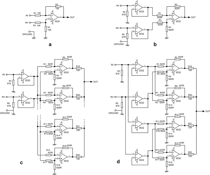
We therefore have the arrangement of Figure 18.29c, with single input buffers (i.e. one per input) and two differential amplifiers, and this reduces the noise output by 2.3 dB to -112.5 dBu, which is quieter than the original 4 × 10 kΩ version by an encouraging 7.4 dB. We do not get a full 3 dB noise improvement because both differential amplifiers are handling the noise from the input buffers, which is correlated and so is not reduced by partial cancellation. The contribution of the input buffer noise is further brought out if we take the next step of using four differential amplifiers (1–4 configuration). There is of course nothing special about using amplifiers in powers of 2. It is perfectly possible to use three or five differential amplifiers in the array, which will give intermediate amounts of noise reduction. If you have a spare opamp section, then put it to work!
So, leaving the input buffers unchanged, we use them to drive an array of four differential amplifiers. These are added on at the dotted lines in the lower half of Figure 18.29c. We get a further improvement, but only by 1.5 dB this time. The output noise is down to -114.0 dBu, quieter than the original 4 × 10 kΩ version by 8.9 dB. You can see that at this point, we are proceeding by decreasing steps, as the input buffer noise is starting to dominate, and there seems little point in doubling up the differential amplifiers again; the amount of hardware could be regarded as a bit excessive, and so would the PCB area occupied. The increased loading on the input buffers is also a bit of a worry.
A more fruitful approach is to tackle the noise from the input buffers by doubling them up as in Figure 18.29d so that each buffer drives only two of the four differential amplifiers (2–4 configuration). This means that the buffer noise will also undergo partial cancellation and will be reduced by 3 dB. There is, however, still the contribution from the differential amplifier noise, and so the actual improvement on the previous version is 2.2 dB, bringing the output noise down to -116.2 dBu, which is quieter than the original 4 × 10 kΩ version by a thumping 11.1 dB. Remember that there are two inputs, and “double buffers” means two buffers per hot and cold input, giving a total of four in the complete circuit.
Since doubling up the input buffers gave us a useful improvement, it’s worth trying again, so we have a structure with quad buffers and four differential amplifiers, as shown in Figure 18.30, where each differential amplifier now has its very own buffer (4–4 configuration). This improves on the previous version by a rather less satisfying 0.8 dB, giving an output noise level of -117.0 dBu, quieter than the original 4 × 10 kΩ version by 11.9 dB. The small improvement we have gained indicates that the focus of noise reduction needs to be returned to the differential amplifier array, but the next step there would seem to be using eight amplifiers, which is not very appealing. Thoughts about ears of corn on chessboards tend to intrude at this point.
This is a good moment to pause and see what we have achieved. We have built a balanced input stage that is quieter than the standard circuit by 11.9 dB using standard components of low cost. We have used increasing numbers of them, but the total cost is still small compared with enclosures, power supplies, etc. On the other hand, the power consumption is clearly several times greater. The technology is highly predictable and the noise reduction reliable; in fact, it’s bulletproof. The linearity is as good as that of a single opamp of the same type, and in the same way there are no HF stability problems.
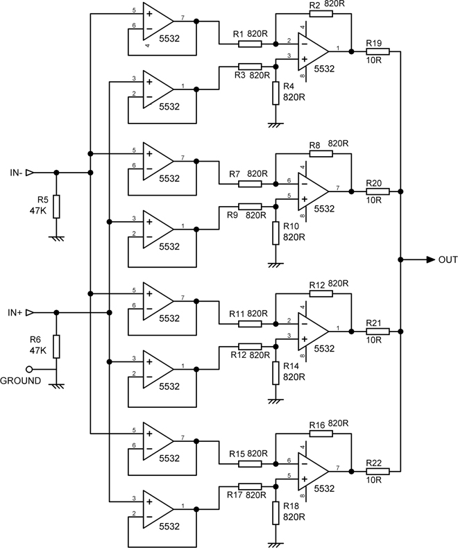
What we have not done is build a balanced input that is quieter than the unbalanced one –we are still 2.0 dB short of that target, but at least we have reached a point at which the balanced input is not obviously noisier.
These noise results are summarised in Table 18.12 at the end of the chapter.
Low-Noise Balanced Inputs in Action
Please don’t think that this examination of low-noise input options is merely a voyage off into pure theory. It has real uses and has been applied in practice, for example in the Cambridge Audio 840W power amplifier, a design of mine which, I might modestly mention in passing, won a CES Innovation Award in January 2008. This unit has both unbalanced and balanced inputs, and conventional technology would have meant that the balanced inputs would have been significantly the noisier of the two. Since the balanced input is the “premium” input, many people would think there was something amiss with this state of affairs. We therefore decided the balanced input had to be quieter than the unbalanced input. Using 5532s in an architecture similar to those outlined earlier, this requirement proved straightforwardly attainable, and the final balanced input design was both economical and quieter than its unbalanced neighbour by a dependable 0.9 dB. Two other versions were evaluated that made the balanced input quieter than the unbalanced one by 2.8 dB and by 4.7 dB at somewhat greater cost and complexity. These were put away for possible future upgrades.
The Signal Transfer Company [18] manufactures a low-noise balanced input card based on these principles which has 47 kΩ input impedances, unity gain, and a noise output of only -115 dBu.
Ultra-Low-Noise Balanced Inputs
In the section on low-noise balanced inputs, we reclined briefly on our laurels, having achieved an economical balanced input stage with output noise at the extremely low level of -117.0 dBu. Regrettably, this is still 2 dB noisier than a simple unbalanced input. It would be wrong to conclude from this that the resources of electronic design are exhausted. At the end of the noise-reduction sequence, we were aware that the dominant noise source was currently the differential amplifier array, and we shrank from doubling up again to use eight amplifiers because of issues of cost and the PCB area occupied. We will take things another step by taking a much more relaxed view of cost (as one does at the “high end”) and see how that changes the game. We will, however, retain some concern about PCB area.
An alternative way to make the differential amplifier array quieter is simply to use opamps that are quieter. These will inevitably be more expensive –much more expensive –than the ubiquitous 5532. Because of the low resistor values around the opamps, we need to focus on low voltage noise rather than low current noise, and there are several that are significantly better than the 5532, as shown by the typical noise density figures in Table 18.11.
Clearly moving to the 5534A will give a significant noise reduction, but since there is only a single opamp per package, and external compensation is needed, the board area used will be much greater. Instead, we will try the LM4562, a bipolar opamp which has finally surpassed the 5532 in performance. The input voltage noise density is typically 2.7 nV/√Hz, substantially lower than the 5 nV/√Hz of the 5532. For applications with low source impedances, this implies a handy noise advantage of 5 dB or more. The LM4562 is a dual opamp and will not take up more space. At the time of writing, it is something like 10 times more expensive than the 5532.
| Opamp | Voltage noise density nV√Hz | Current noise density pA√Hz |
|---|---|---|
| 5532 | 5 | 0.7 |
| 5534A | 3.5 | 0.4 |
| LM4562 | 2.7 | 1.6 |
| AD797 | 0.9 | 2 |
| LT1028 | 0.85 | 1 |
Step One: we replace all four opamps in the differential amplifiers with LM4562s. They are a drop-in replacement with no circuit adjustments required at all. We leave the quad 5532 input buffers in place. The noise output drops by an impressive 1.9 dB, giving an output noise level of -118.9 dBu, quieter than the original 4 × 10 kΩ version by 14.1 dB and only 0.1 dB noisier than the unbalanced stage.
Step Two: replace the quad 5532 buffers with quad LM4562 buffers. Noise falls by only 0.6 dB, the output being -119.5 dBu, but at last we have a balanced stage that is quieter than the unbalanced stage by a small but solid 0.5 dB.
One of the pre-eminent low-noise-with-low-source-resistance opamps is the AD797 from Analog Devices, which has a remarkably low voltage noise at 0.9 nV/√Hz (typical at 1 kHz), but it is a very expensive part, costing between 20 and 25 times more than a 5532 at the time of writing. The AD797 is a single opamp, while the 5532 is a dual, so the cost per opamp is actually 40 to 50 times greater, and more PCB area is required, but the potential improvement is so great we will overlook that…
Step Three: we replace all four opamps in the differential amplifiers with AD797s, putting the 5532s back into the input buffers in the hope that we might be able to save money somewhere. The noise output drops by a rather disappointing 0.4 dB, giving an output noise level of -119.9 dBu, quieter than the original 4 × 10 kΩ version by 15.1 dB.
Perhaps putting those 5532s back in the buffers was a mistake? Our fourth and final move in this game of electronic chess is to replace all the quad 5532 input buffers with dual (not quad) AD797 buffers. This requires another four AD797s (two per input) and is once more not a cheap strategy. We retain the four AD797s in the differential amplifiers. The noise drops by another 0.7 dB, yielding an output noise level of -120.6 dBu, quieter than the original 4 × 10 kΩ version by 15.8 dB and quieter than the unbalanced stage by a satisfying 1.6 dB. You can do pretty much anything in electronics with a bit of thought and a bit of money.
You are probably wondering what happened to the LT1028 lurking at the bottom of Table 18.11. It is true that its voltage noise density is slightly better than that of the AD797, but there is a subtle snag. As described in Chapter 4, the LT1028 has bias-current cancellation circuitry that injects correlated noise currents into the two inputs. These will cancel if the impedances seen by the two inputs are the same, but in moving-magnet amplifier use, the impedances differ radically and the LT1028 is not useful in this application. The input conditions here are more benign, but the extra complication is unwelcome, and I have never used the LT1028 in audio work. In addition, it is a single opamp with no dual version.
This is not, of course, the end of the road. The small noise improvement in the last step we made tells us that the differential amplifier array is still the dominant noise source, and further development would have to focus on this. A first step would be to see if the relatively high current noise of the AD797s is significant with respect to the surrounding resistor values. If so, we need to see if the resistor values can be reduced without degrading linearity at full output. We should also check the Johnson noise contribution of all those 820 Ω resistors; they are generating -123.5 dBu each at room temperature, but of course the partial cancellation effect applies to them as well.
All these noise results are also summarised in Table 18.12.
| Noise output | Improvement on previous version | Improvement over 4 x 10 kΩ diff amp | Noisier than unbal input by: | ||
|---|---|---|---|---|---|
| Buffer type | Amplifier | dBu | dB | dB | dB |
| 5532 voltage–follower | –119.0 | 0.0 dB ref | |||
| None | Standard diff amp 10k 5532 | –104.8 | 0 | 0.0 dB ref | 14.2 |
| None | Single diff amp 820R 5532 | –111.7 | 6.9 | 6.9 | 7.3 |
| Single 5532 | Single diff amp 820R 5532 | –110.2 | 5.4 | 5.4 | 8.8 |
| Single 5532 | Dual diff amp 820R 5532 | –112.5 | 2.3 | 7.4 | 6.5 |
| Single 5532 | Quad diff amp 820R 5532 | –114.0 | 1.5 | 9.2 | 5.0 |
| Dual 5532 | Quad diff amp 820R 5532 | –116.2 | 2.2 | 11.4 | 2.8 |
| Quad 5532 | Quad diff amp 820R 5532 | –117.0 | 0.8 | 12.2 | 2.0 |
| Quad 5532 | Quad diff amp 820R LM4562 | –118.9 | 1.9 | 14.1 | 0.1 |
| Quad LM4562 | Quad diff amp 820R LM4562 | –119.5 | 0.6 | 14.7 | –0.5 |
| Quad 5532 | Quad diff amp 820R AD797 | –119.9 | 0.4 | 15.1 | –0.9 |
| Dual AD797 | Quad diff amp 820R AD797 | –120.6 | 0.7 | 15.8 | –1.6 |
References
[1] Muncy, N. “Noise Susceptibility in Analog and Digital Signal Processing Systems” JAES, Vol. 3, No. 6, Jun 1995, p 447
[2] Williams, T. EMC for Product Designers. Newnes (Butterworth-Heinemann) pub 1992, p 176
[3] Williams, T. As [2] above, p 173
[4] Winder, S. “What’s the Difference?” Electronics World, Nov 1995, p 989
[5] Graeme, J. Amplifier Applications of Opamps. McGraw-Hill, 1999, p 16
[6] Birt, D. “Electronically Balanced Analogue-line Interfaces” Proceedings of the Institute of Acoustics Conference, Windermere, UK, Nov 1990
[7] Fletcher, Ted www.tfpro.com/phpbb/viewtopic.php?f=4&t=164 Accessed Jun 2019
[8] Self, Douglas “Preamplifier 2012” Elektor, Apr/May/Jun 2012
[9] Self, Douglas “A Low Noise Preamplifier with Variable-frequency Tone Controls” Linear Audio, Vol. 5, pub. Jan Didden, pp 141–162
[10] Jung, W., ed Op Amp Applications Handbook. Newnes, Elsevier, 2006
[11] Self, Douglas The Design of Active Crossovers. Focal Press, 2011, p 417
[12] Self, Douglas Ibid, pp 552–560
[13] Self, Douglas Audio Power Amplifier Design 6th edition. Taylor & Francis, 2013, p 142
[14] Whitlock, Bill “A New Balanced Audio Input Circuit for Maximum Common-Mode Rejection in Real World Environments” preprint #4372 presented at the 101st Convention of the Audio Engineering Society, 8–11 Nov 1996, in Los Angeles, CA
[15] Isrealsohn, Joshua www.thatcorp.com/datashts/A_Matter_of_Balance.pdf
[16] Whitlock, Bill US patent 5,568,561 22 Oct 1996
[17] Zwicky, P. Low-Distortion Audio Amplifier Circuit Arrangement US Patent No. 4,567,443 1986
[18] Signal Transfer Company www.signaltransfer.freeuk.com/