CHAPTER 21
Signal Switching
The switching and routing of analogue signals is an important part of signal processing but not one that is easily implemented if accuracy and precision are required. This article focuses on audio applications, but the basic parameters such as isolation and linearity are equally relevant in many fields.
Mechanical Switches
A mechanical switch normally makes a solid unequivocal connection when it is closed, and it is as “on” as the resistance of its contacts and connections allows; these are small fractions of an Ohm and are unlikely to cause trouble in small-signal audio design. Switches are, however, in general terms a good deal less “off”. The insulation resistance may be measured in petaohms, but what does the damage is the inevitable capacitance between contacts. This is usually small in pF but quite large enough to dominate the degree of offness obtainable at high audio frequencies. Its effects naturally depend on the impedance at the “receiving” side of the switch. For all the tests discussed here, this was 10 kΩ.
Using an ALPS SPUN type push switch, at 10 kHz, the offness is only -66 dB, and grounding the unused side of the switch only improves offness by about 2 dB. A graph of the result can be seen in Chapter 22; the offness naturally degrades by 6 dB/octave. Switch capacitance is an important issue in designing mixer routing systems.
In another test, a miniature three-way slide switch gave -70 dB at 10 kHz. Once again, grounding the unused contact at the end of the switch only gave a 4 dB improvement, and it is wise to assume that in general, grounding unused switch sections will not help much.
Switch inter-contact capacitance is quite easy to determine; measure the offness, i.e. the loss of the RC circuit, and since R is known, C can be calculated easily. Once it is known for a given switch construction, it is easy to calculate the offness for different loading resistances. Interestingly, the inter-contact capacitance of switches seems to be relatively constant, even though they vary widely in size and construction. This seems to be because the smaller switches have smaller contacts, with a smaller area, but on the other hand, they are closer together.
Input-Select Switching: Mechanical
Some time ago, Morgan Jones [1] raised the excellent point of crosstalk in the input-select switching of preamplifiers. If the source impedance is significant, then this may be a serious problem. While I agree that his use of a rotary switch with twice the required number of positions and grounding alternate contacts is slightly superior to the conventional use of rotary switches, measuring a popular Lorlin switch type showed the improvement to be only 5 dB. I am also unhappy with all those redundant “Mute” positions between input selections, so when I design a preamp, I normally choose interlocked push-switches rather than a rotary switch. A four-changeover format can then be used to reduce crosstalk.
| 10 kHz | |
|---|---|
| Simple rotary switch | –71 dB |
| Rotary with alternate contacts grounded | –76 dB |
| Two changeover switch | –74 dB |
| Four changeover switch | –95 dB |
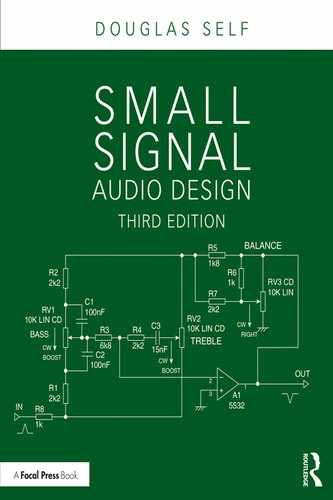
The problem with conventional input select systems like Figure 21.1a is that the various input tracks necessarily come into close proximity, with significant crosstalk through capacitance Cstray to the common side of the switch, i.e. from A to B. Using two changeovers per input side (i.e. four for stereo) allows the intermediate connection B-C to be grounded by the NC contact of the first switch section and keeps the “hot” input A much further away from the common input line D, as shown in Figure 21.1b. Cstray is now much smaller.
The crosstalk data in Table 21.1 was gathered at 10 kHz, with 10 kΩ loading resistances:
The emphasis here is on minimising crosstalk between different sources carrying different signals, as interchannel (L–R) crosstalk is benign by comparison. Interchannel isolation is limited by the placement of Left and Right channels on the same switch, with the contact rows parallel, and limits L–R isolation to -66 dB at 10 kHz with a high 10 kΩ source impedance. Actual source impedances are likely to be lower, with both inter-source and inter-channel crosstalk proportionally reduced; so a more probable 1 kΩ source gives 115 dB of intersource rejection at 10 kHz for the 4-changeover configuration.
The third input of Figure 21.1b has a resistive attenuator intended to bring CD outputs down to the same level as other sources. In this case inter-source crosstalk can be improved simply by back-grounding the attenuator output when it is not in use, so only a two-pole switch is required for good isolation of this input.
The Virtual Contact: Mechanical
What do you do if you need a changeover switch –to select one of two signal sources –but only have a make contact? Here is a technique that can be a lifesaver when you have screwed up on ordering a switch with a long lead time or if you live in a Dilbertian world of last-minute spec changes.
Figure 21.2 demonstrates the principle. With the switch S open, source A goes through voltage-follower A and Rfeed to the output voltage-follower. With the switch closed, the much lower impedance output of voltage-follower B takes over, and the contribution from A is now negligible. To give good rejection of A, the output impedance of follower B must be much, much lower than the value of Rfeed; so an opamp output must be used directly. Figure 21.3 shows how good the rejection of A can be using 5532 opamps as the voltage followers.

Figure 21.2 The virtual contact concept. When the switch S is closed, the signal B over-rides signal A.
At first, this technique looks a bit opamp-intensive. However, there is often no need to use dedicated voltage-followers if a similar low-impedance feed is available from a previous stage that uses an opamp with a large amount of negative feedback. Likewise, the output voltage-follower may often be dispensed with if the following load is reasonably high.

Figure 21.3 Rejection of signal A for 2k2, 4k7, and 10 kΩ Rfeed resistors, using 5532 opamps.
There is also the rejection of B when the switch is open to consider. The impedance of Rfeed means there is the potential for capacitative crosstalk across the open switch contacts. The amount depends on the value if Rfeed and on switch construction.
If the offness of B is more important than the offness of A, then Rfeed should be a lower value, to minimise the effects of the capacitance. Do not make Rfeed too low, as A drives through it into effectively a short circuit when B is selected.
If the offness of A is more important, Rfeed should be higher to increase its ratio to the output impedance of B; be aware that making it too high may introduce excessive Johnson noise.
The rejection of A shown in Figure 21.3 worsens at high frequencies, as the dominant pole of opamp B reduces its open-loop gain and the output impedance rises. The slopes are 6 dB/octave as usual.
This technique is particularly useful for switching between three sources with a centre-off toggle switch.
Relay Switching
Any electronic switching technique must face comparison with relays, which are still very much with us. Relays give total galvanic isolation between control and signal, zero contact distortion, and in audio terms have virtually unlimited signal-handling capability. They introduce negligible series resistance, and shunt leakage to ground is usually also negligible. Signal offness can be very good, but as with other kinds of switching, this depends on intelligent usage. There will always be capacitance between open contacts, and if signal is allowed to crosstalk through this to nominally off circuitry, the “offness” will be no better than other kinds of switching.
Obviously relays have their disadvantages. They are relatively big, expensive, and not always as reliable as more than a hundred years of development should have made them. Their operating power is significant, though it can be reduced by circuitry that applies full voltage to pull in the relay and then a lower voltage to keep it closed. Some kinds of power relay can introduce disastrous distortion if used for switching audio because the signal passes through the magnetic soft-iron frame; however, such problems are likely to be confined to the output circuits of large power amplifiers. For small-signal switching, the linearity of relay contacts can normally be regarded as perfect.
Electronic Switching
Electronic switching is usually implemented with CMOS analogue gates, of which the well-known 4016 is the most common example, and these are examined first. However, there are many special applications in which discrete JFETs provide a better solution, so these are dealt with in the second part.
Switching with CMOS Analogue Gates
CMOS analogue gates, also known as transmission gates, are quite different from the CMOS logic gates in the 4000 series, though the underlying process technology is the same. Analogue gates are bilateral, which means that either of the in/out leads can be the input or output; this is emphatically not true for logic gates. The “analogue” part of the name emphasises that they are not restricted to fixed logic levels but pass whatever signal they are given with low distortion. The “low” there requires a bit of qualification, as will be seen later.
When switched on, the connection between the two pins is a resistance which passes current in each direction as usual, depending on the voltage between the two terminals. Analogue gates have been around for a long time and are in some ways the obvious method of electronic switching. They do, however, have significant drawbacks.
Analogue gates like the 4016 are made up of two MOS FETs of opposite polarity connected back to back. The internal structure of a 4016 analogue gate is shown in Figure 21.4. The two transmission FETs with their protective diodes are shown on the right; on the left is the control circuitry. A and B are standard CMOS inverters whose only function is to sharpen up the rather soggy voltage levels that 4000-series CMOS logic sometimes provides. The output of B directly controls one FET, and inverter C develops the anti-phase control voltage for the FET of opposite polarity, which requires an inverted gate voltage to turn it on or off.

Figure 21.4 The internal circuitry of a 4000-series analogue gate.
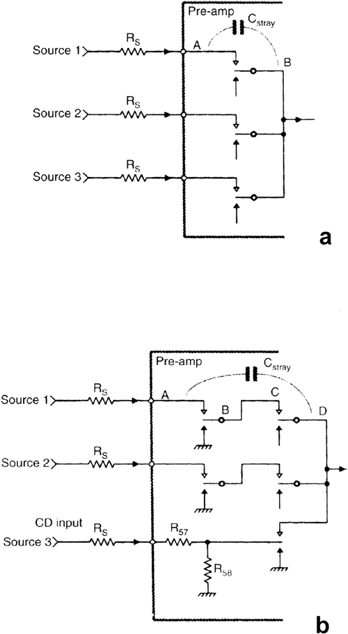
MOS FETS are of the enhancement type, requiring a voltage to be applied to the gate to turn them on; (in contrast, JFETs work in depletion mode and require a gate voltage to turn them off), so as the channel approaches the gate voltage, the device turns off more. An analogue gate with only one polarity of FET would be of little use because Ron would become very high at one extreme of the voltage range. This is why complementary FETs are used; as one polarity finds its gate voltage decreasing, turning it off, the other polarity has its gate voltage increasing, turning it more on. It would be nice if this process cancelled out so the Ron was constant, but sadly it just doesn’t work that way. Figure 21.5 shows how Ron varies with input voltage, and the peaky curve gives a strong hint that something is turning on as something else turns off.
Figure 21.5 Typical variation of the gate series resistance Ron for the 4016. There is less variation with the +15 V supply.
Figure 21.5 also shows that Ron is lower and varies less when the higher supply voltage is used; since these are enhancement FETs the on-resistance decreases as the available control voltage increases. If you want the best linearity, then always use the maximum rated supply voltage.
Since Ron is not very linear, the smaller its value the better. The 4016 Ron is specified as 115 Ω typical, 350 Ω max, over the range of input voltages and with a 15 V supply. The 4066 is a version of the 4016 with lower Ron, 60 Ω typical, 175 Ω max under the same conditions. This option can be very useful both in reducing distortion and improving offness, and in most cases, there is no point in using the 4016. The performance figures given in what follows all assume the use of the 4066 except where stated.
CMOS Gates in Voltage Mode
Figure 21.6 shows the simplest and most obvious way of switching audio on and off with CMOS analogue gates. This series configuration is in a sense the “official” way of using them, the only snag being that it doesn’t work very well.
Figure 21.7 shows the measured distortion performance of the simple series gate using the 4016 type. The distortion performance is a long way from brilliant, exceeding 0.1% just above 2 Vrms. These tests, like most in this section, display the results for a single sample of the semiconductor in question. Care has been taken to make these representative, but there will inevitably be some small variation in parameters like Ron. This may be greater when comparing the theoretically identical products of different manufacturers.
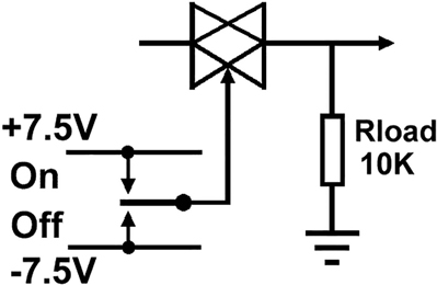
Figure 21.6 Voltage-mode series switching circuit using analogue gate.
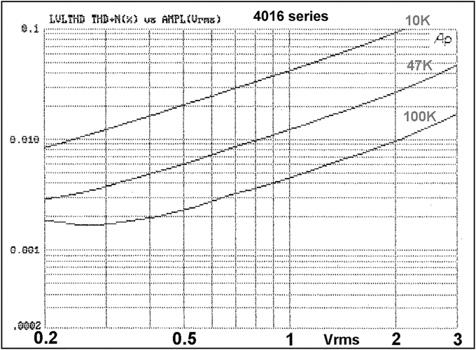
Figure 21.7 4016 series-gate THD versus level, with different load resistances.
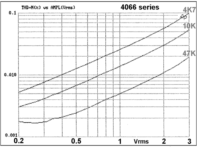
Figure 21.8 4066 THD versus level, with different load resistances.
Replacing the 4016 gate with a 4066 gives a reliable improvement due to the lower Ron. THD at 2 Vrms (10 kΩ load) has dropped to a third of its previous level (see Figure 21.8). There seems to be no downside to using 4066 gates instead of the more common and better-known 4016, and they are used exclusively from this point on unless otherwise stated. Likewise, using multiple gates in parallel reduces distortion; see Figure 21.9.
The distortion is fairly pure second harmonic, except at the highest signal levels, where higher-order harmonics begin to intrude. This is shown in Figures 21.8 and 21.9 by the straight line plots beginning to bend upwards above 2 Vrms.
Analogue gate distortion is flat with frequency as far as audio is concerned, so no plots of THD versus frequency are shown; they would just be a rather uninteresting set of horizontal lines.
This circuit gives poor offness when off, as shown by Figure 21.10. The offness is limited by the stray capacitance in the package feeding through into the relatively high load impedance. If this is 10 kΩ, the offness is only -48 dB at 20 kHz, which would be quite inadequate for most applications. The load impedance could be reduced below 10 kΩ to improve offness –for example, 4k7 offers about a 7 dB improvement –but this degrades the distortion, which is already poor at 0.055% for 3 Vrms, to 0.10%.

Figure 21.9 THD versus level, for different numbers of paralleled 4066 gates.
Using 4066 gates instead of 4016s does not improve offness in this configuration. The internal capacitance that allows signals to leak past the gate seems to be the same for both types. The maximum signal level that can be passed through (or stopped) is limited by the CMOS supply rails and conduction of the protection diodes. While it would in some cases be possible to contrive a bootstrapped supply to remove this limitation, it is probably not a good route to head down.
Figure 21.11 shows a CMOS three-way switch. When analogue gates are used as a multi-way switch, the offness problem is much reduced, because capacitative feedthrough of the unwanted inputs is attenuated by the low Ron looking back into the (hopefully) low impedance of the active input, such as an opamp output. If this is not the case, then the crosstalk from nominally off inputs can be serious.
In this circuit, the basic poor linearity is unchanged, but since the crosstalk problem is much less, there is often scope for increasing the load impedance to improve linearity. This makes Ron a smaller proportion of the total resistance. The control voltages must be managed so that only one gate is on at a time, so there is no possibility of connecting two opamp outputs together.

Figure 21.10 4066 offness versus load resistance. -48 dB at 20 kHz with a 10kΩ load.
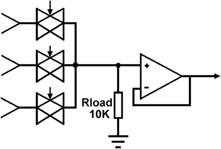
Figure 21.11 A one-pole, three way switch made from analogue gates.
It may appear that if you are implementing a true changeover switch, which always has one input on, the resistor to ground is redundant, and just a cause of distortion. Omitting it is, however, very risky, because if all CMOS gates are off together even for an instant, there is no DC path to the opamp input, and it will register its displeasure by snapping its output to one of the rails. This does not sound nice.
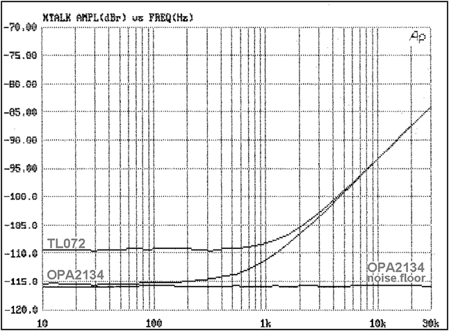
Figure 21.12 Voltage-mode changeover circuit offness for TL072 and OPA2134. 10kΩ load.
Figure 21.12 shows the offness of a changeover system, for two types of FET-input opamps. The offness is much improved to -87 dB at 20 kHz, an improvement of 40 dB over the simple series switch; at the high-frequency end, however, it still degrades at the same rate of 6 dB/octave. It is wellknown that the output impedance of an opamp with negative feedback increases with frequency at this rate, as the amount of internal gain falls, and this effect is an immediate suspect. However, there is actually no detectable signal on the opamp output (as shown by the lowest trace), and it is also not very likely that two completely different opamps would have exactly the same output impedance. I was prepared for a subtle effect, but the true explanation is that the falling offness is simply due to feedthrough via the internal capacitance of the analogue gate.
It now remains to explain why the OPA2134 apparently gives better offness in the flat low-frequency region. In fact it does not; the flat parts of the trace represent the noise floor for that particular opamp. The OPA2134 is a more sophisticated and quieter device than the TL072, and this is reflected in the lower noise floor.
There are two linearity problems. First, the on-resistance itself is not totally linear. Second and more serious, the on-resistance is modulated when the gates move up and down with respect to their fixed control voltages.
It will by now probably have occurred to most readers that an on/off switch with good offness can be made by making a changeover switch with one input grounded. This is quite true, but since much better distortion performance can be obtained by using the same approach in current mode, as explained in what follows, I am not considering it further here.
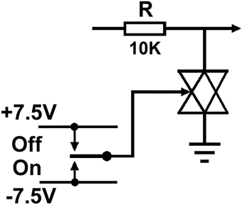
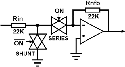
Figure 21.13 shows a shunt muting circuit. This gives no distortion in the “ON” state because the signal is no longer going through the Ron of a gate. However, the offness is limited by the Ron, forming a potential divider with the series resistor R; the latter cannot be very high in value, or the circuit noise will be degraded. There is, however, the advantage that the offness plot is completely flat with frequency. Note that the ON and OFF states of the control voltage are now inverted.
Table 21.2 gives the measured results for the circuit, using the 4066. The offness can be improved by putting two or more of these gates in parallel, but since doubling the number N only gives 6 dB improvement, it is rarely useful to press this approach beyond four gates.
| N gates | Offness |
|---|---|
| 1 | –37 dB |
| 2 | –43 dB |
| 4 | –49 dB |
CMOS Gates in Current Mode
Using these gates in current mode –usually by defining the current through the gate with an input resistor and dropping it into the virtual-earth input of a shunt-feedback amplifier –gives much superior linearity. It removes the modulation of channel resistance as the gate goes up and down with respect to its supply rails and, in its more sophisticated forms, can also remove the signal voltage limit and improve offness.
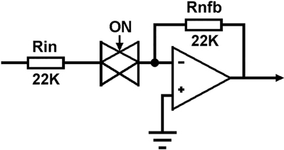
Figure 21.14 The simplest version of a current-mode on/off switch.
Figure 21.14 shows the simplest version of a current-mode on/off switch. An important design decision is the value of Rin and Rnfb, which are often equal to give unity gain. Too low a value increases the effect of the non-linear Ron, while too high a value degrades offness, as it makes the gate stray capacitance more significant and also increases Johnson noise. In most cases, 22 kΩ is a good compromise.
Table 21.3 gives the distortion for +20 dBu (7.75 Vrms) in/out and shows that it is now very low compared with voltage-mode switchers working at much lower signal levels; compare the table data with Figures 21.8 and 21.9. The increase in THD at high frequencies is due to a contribution from the opamp. However, the offness is pretty poor and would not be acceptable for most applications. The problem is that with the gate off, the full signal voltage appears at the gate input and crosstalks to the summing node through the package’s internal capacitance. In practical double-sided PCB layouts, the inter-track capacitance can usually be kept very low by suitable layout, but the internal capacitance of the gate is inescapable.
| 1 kHz | 10 kHz | 20 kHz | |
|---|---|---|---|
| THD via 4016, +20 dBu | 0.0025% | 0.0039% | 0.0048% |
| THD: 4016 shorted, +20 dBu | 0.0020% | 0.0036% | 0.0047% |
| Offness | –68 dB | –48 dB | –42 dB |

Figure 21.15 Current-mode switch circuit with breakthrough prevention resistor Rin2.
In Figures 21.14 and 21.15, the CMOS gate is powered from a maximum of ±7.5 V. This means that in Figure 21.14, signal breakthrough begins at an input of 5.1 Vrms. This is much too low for opamps running off their normal rail voltages, and several dB of headroom is lost.
Figure 21.15 shows a partial cure for this. Resistor Rin2 is added to attenuate the input signal when the CMOS gate is off, preventing breakthrough. There is no effect on signal gain when the gate is on, but the presence of Rin2 does increase the noise gain of the stage.
As with all shunt-feedback stages, this circuit introduces a phase inversion, which is sometimes convenient but usually not.
CMOS Series-Shunt Current Mode
We now extravagantly use two 4016 CMOS gates, as shown in Figure 21.16.
When the switch is on, the series gate passes the signal through as before; the shunt gate is off and has no effect. When the switch is off, the series gate is off and the shunt gate is on, sending almost all the signal at A to ground so that the remaining voltage is very small. The exact value depends on the 4016 specimen and its Ron value but is about 42 dB below the input voltage. This deals with the offness (by greatly reducing the signal that can crosstalk through the internal capacitance) and also increases the headroom by several dB, as there is now effectively no voltage signal to breakthrough when it exceeds the rails of the series gate.
Two antiphase control signals are now required. If you have a spare analogue gate, it can generate the inverted control signal, as shown in Figure 21.17.
Figure 21.17 Generating antiphase control signals with a spare analogue gate.
The distortion generated by this circuit can be usefully reduced by using two gates in parallel for the series switching, as in Table 21.4; this gate-doubling reduces the ratio of the variable Ron to the fixed series resistor and so improves the linearity. Using two in parallel is sufficient to render the distortion negligible. (The higher distortion figures at 10 kHz and 20 kHz are due to distortion generated by the TL072 opamp used in the measurements.)
As before, the input and output levels are +20 dBu, well above the nominal signal levels expected in opamp circuitry; measurements taken at more realistic levels would show only noise.
Discrete FETs have lower Ron than analogue gates. If a J111 JFET is used as the shunt-switching element, the residual signal at A is further reduced, to about 60 dB below the input level, with a consequent improvement in offness, demonstrated by the bottom row in Table 21.4. This could also be accomplished by using two or more CMOS gates for the shunt switching.
Control Voltage Feedthrough in CMOS Gates
When an analogue gate changes state, some energy from the control voltage passes into the audio path via the gate-channel capacitance of the switching FETs, through internal package capacitances, and through any stray capacitance designed into the PCB. Since the control voltages of analogue gates move snappily due to the internal inverters, this typically puts a click rather than a thump into the audio. Attempts to slow down the control voltage going into the chip with RC networks are not likely to be successful for this reason. In any case, slowing down the control voltage change simply converts a click to a thump; the FET gates are moving through the same voltage range, and the feedthrough capacitance has not altered, so the same amount of electric charge has been transferred to the audio path –it just gets there more slowly.
| 1 kHz | 10 kHz | 20 kHz | |
|---|---|---|---|
| THD via 4016 × 1, +20 dBu | 0.0016% | 0.0026% | 0.0035% |
| THD via 4016 × 2, +20 dBu | 0.0013% | 0.0021% | 0.0034% |
| THD 4016 shorted, +20 dBu | 0.0013% | 0.0021% | 0.0034% |
| Offness 4016 × 1 | –109 dB | –91 dB | –86 dB |
| Offness 4016 × 1, J111 | < –116 dB | –108 dB | –102 dB |
The only certain way to reduce the effect of transient feedthrough is to soak it up in a lower value of load resistor. The same electric charge is applied to a lower resistor value (the feedthrough capacitance is tiny and controls the circuit impedance), so a lower voltage appears. Unfortunately, reducing the load tends to increase the distortion, as we have already seen; the question is if this is acceptable in the intended application.
CMOS Gates at Higher Voltages
Analogue gates of the 4016/4066 series have a voltage range of ±7.5 V, so they cannot directly switch signals from opamps running from the usual ±15 V or ±17 V rails. The classic device for solving this problem is the DG308 from Maxim. The absolute maximum supply rails are ±22 V, and the maximum signal range is specified as ±15 V. The Ron is typically between 60 and 95 Ω with ±15 V supply rails, comparable with a 4016 on ±7.5 V rails. The DG308 is not pin-compatible with the 4016/4066. The DG308 has been around for a long time, and it has always been significantly more expensive than 4016/4066. That situation continues today.
CMOS Gates at Low Voltages
So far, we have generally assumed that the CMOS analogue gates will be run from the maximum-rated rail voltages of ±7.5 V to maximise the linearity of types such as the 4016/4066. As noted in Chapter 5, there is nowadays much interest in designing audio paths that can give decent quality when run from +5 V, the power typically being drawn from a USB port or similar digital source; what I call 5-volt fidelity. The 4016/4066 gates work poorly under these conditions; the supply voltage is reduced to a third of the maximum, and this gives very bad linearity.
The answer is to use something designed for the job. The DG9424 from Vishay-Siliconix is rated for maximum supplies of ±6 V and works well running from a single 5 V supply. In this case, its typical Ron is 3.4 Ω, which is much superior to the range of Ron shown for the 4016 in Figure 21.5. Once again, a higher supply voltage means a lower Ron and less distortion; running the DG9424 from ±5 V reduces the typical Ron to 2 Ω, and using the maximum ±6 V rails reduces it further to typically 1.8 Ω. This is a considerable advance on the older parts.

Figure 21.18 shows the distortion in series mode at various signal levels when driving a 10 kΩ load. When making the measurements, I found that for outputs greater than 1.5 V and above 32 kHz, the analogue switches entered a high-distortion mode that gave about 0.06% THD. Whether that is a typical finding I am not sure, but it is unlikely to cause problems unless you are handling high-level ultrasonic signals. I also found that distortion was at a minimum for a single +8 V supply, which does not fit in well with the official Ron specs; the reason for this is currently unknown. The DG9424 is pin-compatible with the DG308.
CMOS Gate Costs
Table 21.5 shows the prices for SMD format in small quantities at January 2020. The prices will obviously be much lower for quantity production, but the ratios between them should be roughly the same.
You can see that the DG308 is a good deal more costly than the humbler 4016. The DG9424, being something of a specialised part, is more expensive again. The surprise is that the 4016 comes out as more costly as the 4066. The only explanation I can think of is that, as mentioned earlier, the 4066 always works better, and there seems no reason why the 4016 should ever be used. Perhaps that means they are manufactured in smaller quantities and are therefore pricier.
| Analogue gate | Price each GBP |
|---|---|
| 4016 | 0.386 |
| 4066 | 0.314 |
| DG308 | 1.73 |
| DG9424 | 1.83 |
Discrete JFET Switching
Having looked in detail at analogue switching using CMOS gates and having seen how well they can be made to work, you might be puzzled as to why anyone should wish to perform the same function with discrete JFETs. There are at least two advantages in particular applications.
First, JFETs can handle the full output range of opamps working from maximum supply rails, so higher signal levels can often be switched directly without requiring opamps to convert between current and voltage mode.
Second, the direct access to the device gate allows relatively slow changes in attenuation (though still measured in milliseconds, for reasons that will emerge) rather than the rapid on-off action which CMOS gates give as a result of their internal control-voltage circuitry. This is vital in creating mute circuits that essentially implement a fast fade rather than a sharp cut and so do not generate clicks and thumps by abruptly interrupting the signal. The downside is that they require carefully tailored voltages to drive the gates, and these cannot always be conveniently derived from the usual opamp supply rails.
The Series JFET Switch in Voltage Mode
The basic JFET series switching circuit is shown in Figure 21.19. With the switch open, there is no other connection to the gate other than the bootstrap resistor Rboot, Vgs is zero, and so the FET is on. When the switch is closed, the gate is pulled down to a sufficiently negative voltage to ensure that the FET is biased off even when the input signal is at its negative limit.
The JFET types J111 and J112 are specially designed for analogue switching and are pre-eminent for this application. The channel on-resistances are low and relatively linear. This is a depletion-mode FET, which requires a negative gate voltage to actively turn it off. The J111 requires a more negative Vgs to ensure it is off but in return gives a lower Rds(on) which means lower distortion.
The J111 and J112 (and J113) are members of the same family –in fact, they are the same device, selected for gate/channel characteristics, unless I am much mistaken. Table 21.6 shows how the J111 may need 10 V to turn it off but gives a 30 Ω on-resistance or Rds(on) with zero gate voltage. In contrast, the J112 needs only 5.0 V at most to turn it off but has a higher Rds(on) of 50 Ω. The trade-off is between ease of generating the gate control voltages and linearity. The higher the Rds(on), the higher the distortion, as this is a non-linear resistance.
| J111 | J112 | J113 | |
|---|---|---|---|
| Vgs(off) min | –3.0 | –1.0 | –0.5 V |
| Vgs(off) max | –10 | –5.0 | –3.0 V |
| Rds(on) | 30 | 50 | 100 |
FET tolerances are notoriously wide, and nothing varies more than the Vgs characteristic. It is essential to take the full range into account when designing the control circuitry.
Both the J111 and J112 are widely used for audio switching. The J111 has the advantage of the lowest distortion, but the J112 can be driven directly from 4000 series logic running from +/-7.5 V rails, which is often convenient. The J113 appears to have no advantage to set against its high Rds(on) and is rarely used – I have never even seen one. The circuits shown use either J111 or J112, as appropriate. The typical version used is shown, along with typical values for associated components.
Figure 21.19 has Source and Drain marked on the JFET. In fact, the J11x devices appear to be perfectly symmetrical, and it seems to make no difference which way round they are connected, so further diagrams omit this. As JFETs, in practical use, they are not particularly static sensitive.
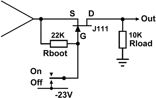
Figure 21.19 The basic JFET switching circuit, with gate bootstrap resistor.
The off voltage must be sufficiently negative to ensure that Vgs never becomes low enough to turn the JFET on. Since a J111 may require a Vgs of -10 V to turn it off, the off voltage must be 10 V below the negative saturation point of the driving opamp –hence the -23 V rail. This is not exactly a convenient voltage, but the rail does not need to supply much current, and the extra cost in something like a mixing console is relatively small.
To turn a JFET on, the Vgs must be held at zero volts. That sounds simple enough, but it is actually the more difficult of the two states. Since the source is moving up and down with the signal, the gate must move up and down in exactly the same way to keep Vgs at zero. This is done by bootstrap resistor Rboot in Figure 21.19. When the JFET is off, DC flows through this resistor from the source; it is therefore essential that this path be DC coupled and fed from a low impedance such as an opamp output, as shown in these diagrams. The relatively small DC current drawn from the opamp causes no problems.
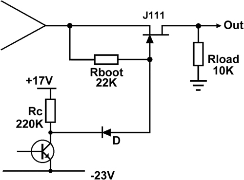
Figure 21.20 is a more practical circuit using a driver transistor to control the JFET. (If you had a switch contact handy, you would presumably use it to control the audio directly.) The pull-up resistor Rc keeps diode D reverse biased when the JFET is on; this is its sole function, so the value is not critical. It is usually high to reduce power consumption. I have used anything between 47 kΩ and 680 kΩ with success.
Sometimes DC-blocking is necessary if the opamp output is not at a DC level of 0 V. In this case, the circuit of Figure 21.21 is very useful; the audio path is DC blocked but not the bootstrap resistor, which must always have a DC path to the opamp output. Rdrain keeps the capacitor voltage at zero when the JFET is held off.
Figure 21.22 shows the distortion performance with a load of 10 kΩ. The lower curve is the distortion from the 5532 opamp alone. The signal level was 7.75 Vrms (+20 dBu).
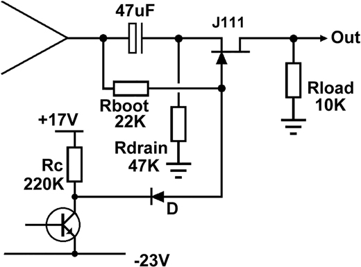
Figure 21.21 The JFET switching circuit with a DC-blocking capacitor.

Figure 21.22 The JFET distortion performance with a load of 10 kΩ.

Figure 21.23 The JFET distortion performance versus loading.
Figure 21.23 shows the distortion performance with various heavier loadings, from 10 kΩ down to 1 kΩ. As is usual in the world of electronics, heavier loading makes things worse. In this case, it is because the non-linear Ron becomes a more significant part of the total circuit resistance. The signal level was 7.75 Vrms (+20 dBu).
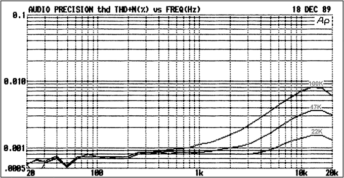
Figure 21.24 The distortion performance with different values of bootstrap resistor.
Figure 21.24 shows the distortion performance with different values of bootstrap resistor. The lower the value, the more accurately the drain follows the source at high audio frequencies, and so the lower the distortion. The signal level was 7.75 Vrms (+20 dBu) once again. There appears to be no disadvantage to using bootstrap resistor of 22 kΩ or so, except in special circumstances, as explained in what follows.
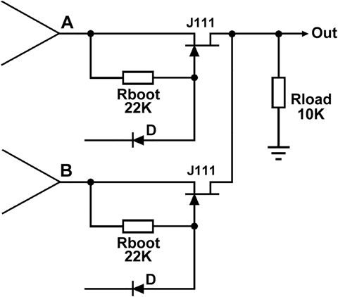
Two series JFET switches can be simply combined to make a changeover switch, as shown in Figure 21.25. The valid states are A on, B on, or both off. Both on is not a good option because the two opamps will then be driving each other’s outputs through the JFETs.
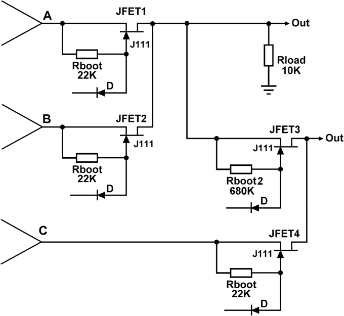
It is possible to cascade FET switches, as in Figure 21.26, which is taken from a real mixing console application. Here the main output is switched between A and B as before, but a second auxiliary output is switched between this selection and another input C by JFET3 and JFET4. The current drawn by the second bootstrap resistor Rboot2 must flow through the Rds(on) of the first FET and will thus generate a small click. Rboot2 is therefore made as high as possible to minimise this effect, accepting that the distortion performance of the JFET3 switch will be compromised at HF; this was acceptable in the application as the second output was not a major signal path. The bootstrap resistor of JFET4 can be the desirable lower value, as this path is driven direct from an opamp.
The Shunt JFET Switch in Voltage Mode
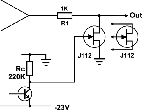
The basic JFET shunt-switching circuit is shown in Figure 21.27. Like the shunt analogue gate mute, it gives poor offness but good linearity in the ON state, so long as its gate voltage is controlled so it never allows the JFET to begin conducting. Its great advantage is that the depletion JFET will be in its low-resistance state before and during circuit power-up and can be used to mute switch-on transients. Switch-off transients can also be effectively muted if the drive circuitry is configured to turn on the shunt FETs as soon as the mains disappears and keep them on until the various supply rails have completely collapsed.
I have used the circuit of Figure 21.27 to mute the turn-on and turn-off transients of a hi-fi preamplifier. Since this is an output that is likely to drive a reasonable length of cable, with its attendant capacitance, it is important to keep R1 as low as possible to minimise the possibility of a drooping treble response. This means that the Rds(on) of the JFET puts a limit on the offness possible. The output series resistor R1 is normally in the range 47–100 Ohms, when it has as its only job the isolation of the output opamp from cable capacitance. Here it has a value of 1 kΩ, which is a distinct compromise –it is not suited for use with very long cables. Even with this value, the muting obtained was not quite adequate at -27 dB, so two J111s were used in parallel, giving a further -6 dB of attenuation. The resulting -33 dB across the audio band was sufficient to render the transients inaudible. The offness is not frequency dependent, as the impedances are low, and so stray capacitance is irrelevant.
JFETs in Current Mode
JFETS can be used in the current mode, just as for analogue gates. Figure 21.28 shows the basic muting circuit, with series FET switching only. Rin2 attenuates the signal seen by the FET when it is off, to prevent breakthrough; its presence means that the gain of the circuit is somewhat less than unity with the values shown, but the gain may be readily adjusted by altering the value of Rnfb. Figure 21.29 illustrates the distortion performance and Figure 21.30 the offness of this circuit. Neither is startlingly good.
In designing a mute block, we want low distortion AND good offness at the same time, so the series-shunt configuration, which proved highly effective with CMOS analogue gates, is the obvious choice. The basic circuit is shown in Figure 21.31; the distortion performance is illustrated in Figure 21.32 and the offness in Figures 21.33 and 21.34. Capacitor C1 across the feedback resistor is usually required to ensure HF stability due to the FET capacitances hanging on the summing node at D.
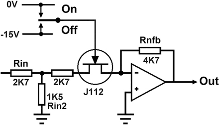

Due to the shunt-feedback configuration, this circuit introduces a phase inversion. I have often been forced to follow this circuit with another inverting stage that does nothing except get the phase right again. In this situation, it is sometimes advantageous to put the inverting stage before the mute block so that any crosstalk to its sensitive summing node is muted with the signal by the following mute block.
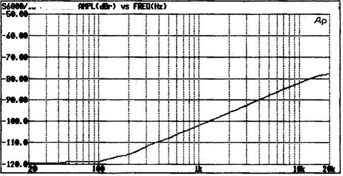
Figure 21.30 Offness of the single-FET circuit in Figure 21.28. It only manages -82 dB at 10 kHz.
The control voltages to the series and shunt JFETs are complementary as with the CMOS version, but now they can be slowed down by RC networks to make the operation gradual, as shown in Figure 21.35. The exact way in which the control voltages overlap is easy to control, but the Vgs/resistance law of the FET is not (and it is about the most variable FET parameter there is), and so the overlap of FET conduction is rather variable. However, I should say at once that this system does work and works well enough to go in top-notch mixing consoles. As you go into the muted condition, the series JFET turns off and the shunt JFET turns on, and if the overlap gets to be too much in error, the following bad things can happen:
- If the shunt FET turns on too early, while the series JFET is still mostly on, a low-resistance path is established from the opamp VE point to ground, causing a large but brief rise in stage noise gain. This produces a “chuff” of noise at the output as muting occurs.
- If the shunt FET turns on too late, so the series JFET is mostly off, the large signal voltage presented to the series FET causes visibly serious distortion. I say “visibly” because it is well known that even quite severe distortion is not obtrusive if it occurs only briefly. The transition here is usually fast enough for this to be the case; it would not, however, be a practical way to generate a slow fade. The conclusion is that we should err on the side of distortion rather than noise.
Reducing Distortion by Biasing
The distortion generated by this circuit block is of considerable importance, because if the rest of the audio path is made up of 5532 opamps –which is likely in professional equipment –then this stage can generate more distortion than the rest of the signal path combined and dominate this aspect of the performance. It is therefore worth examining any way of increasing the linearity that we can think of.
We have already noted that to minimise distortion, the series JFET should be turned on as fully as possible to minimise the value of the non-linear Rds(on). When a JFET has a zero gate-source voltage, it is normally considered fully on. It is, however, possible to turn it even more on than this.
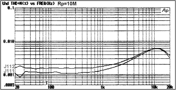
Figure 21.32 The THD of the mute bloc in Figure 21.35 with R = 4k7 and Rp= 10 MΩ. The increase in JFET distortion caused by using a J112 rather than a J111 is shown. The rising distortion above 1 kHz comes from the opamp.
The technique is to put a small positive voltage on the gate, say about 200–300 mV. This further reduces the Rds(on) in a smoothly continuous manner, without forward biasing the JFET gate junction and injecting DC into the signal path. This is accomplished in Figure 21.35 by the simple addition of Rp, which allows a small positive voltage to be set up across the 680K resistor R1. The value of Rp is usually in the 10–22 MΩ range for the circuit values shown here.
Care is needed with this technique, because if temperatures rise, the JFET gate diode may begin to conduct after all, and DC will leak into the signal path, causing thumps and bangs. In my experience, 300 mV is about the upper safe limit for equipment that gets reasonably warm internally, i.e. about 50°C. Caution is the watchword here, for unwanted transients are much less tolerable than slightly increased distortion.
As with analogue CMOS gates, an important consideration with this circuit is the impedance at which it works, i.e. the values of Rin and Rnfb. These are usually of equal resistance for unity gain, so we will call their value R:
- Raising R reduces distortion because it minimises the effect of Rds(on) variation in the series JFET.
- Lowering R reduces the noise generated by the circuit and improves offness as it reduces the effect of stray capacitances. It also reduces the effect of control-voltage feedthrough via the gate-channel capacitances.
Figures 21.33 and 21.34 examine how the offness of the circuit is affected by using values of 4k7 and 22 kΩ. The latter gives -110 dB rather than -120 dB at 10 kHz. In my not inconsiderable experience with this circuit, R = 4k7 is the best choice when J112s are used. Values below 4k7 are not usual, as distortion will increase as the JFET Rds(on) becomes a larger part of the total resistance in the circuit. The loading effect of Rin on the previous stage must also be considered.
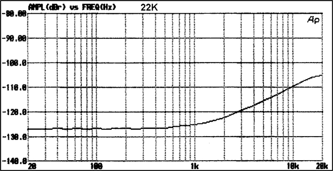
Figure 21.33 Offness of mute bloc in Figure 21.35 with Rin = Rnfb = 22k.
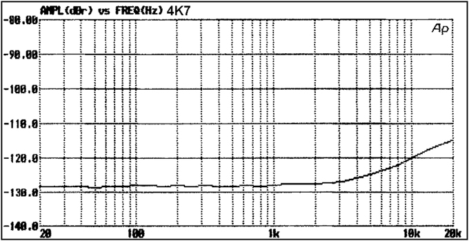
Figure 21.34 Offness of mute bloc in Figure 21.35 with Rin = Rnfb = 4k7. Offness is better, and the noise floor (the flat section below 2 kHz) has been lowered by about 2 dB.
JFET Drive Circuitry
The series-shunt mute bloc requires two complementary drive voltages, and these are most easily generated by 4000-series CMOS running from +/-7.5 V rails. NAND gates are shown here, as they are convenient for interfacing with other bits of control logic, but any standard CMOS output can be used. It is vital that the JFET gates get as close to 0 V as possible, ensuring that the series gate can be fully on and give minimum distortion, so the best technique is to run the logic from these +/- rails and use diodes to clamp the gates to 0 V.
Thus, in Figure 21.35, when the mute bloc is passing signal, the signal from gate A is high, so D1 is reverse-biased and the series JFET TR1 gate is held at 0 V by R1, keeping it on. (The role of Rp will be explained in a moment.) Meanwhile, D2 is conducting, as the NAND-gate output driving it is low, so the shunt JFET TR2 gate is at about -7 V, and it is firmly switched off. This voltage is more than enough to turn off a J112 but cannot be guaranteed to turn off a J111, which may require -10 V (see Table 21.6). This is one reason why the J112 is more often used in this application –it is simpler to generate the control voltages. When the mute bloc is off, the conditions are reversed, with the output of A low, turning off TR1, and the output of B high, turning on TR2.
When switching audio signals, an instantaneous cut of the signal is sometimes not what is required. When a non-zero audio signal is abruptly interrupted, there is bound to be a click. Perhaps surprisingly, clever schemes for making the instant of switching coincide with a zero-crossing give little improvement. There may no longer be a step-change in level, but there is still a step-change in slope, and the ear once more interprets this discontinuity as a click.
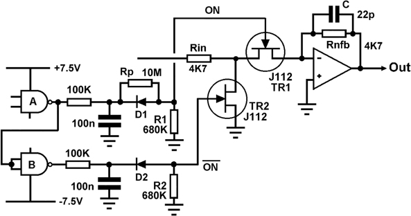
Figure 21.35 Circuitry to generate drive voltages for series-shunt JFET mute bloc.
What is really needed is a fast fade over about 10 msec. This is long enough to prevent clicks without being so slow that the timing of the event becomes sloppy. This is normally only an issue in mixing consoles, where it is necessary for things to happen in real time. Such fast-fade circuits are often called “mute blocks” to emphasise that they are more than just simple on-off switches. Analogue gates cannot be slowly turned on and off due to their internal circuitry for control-voltage generation, so discrete JFETs must be used. Custom chips to perform the muting function have been produced, but the ones I have evaluated have been expensive, single-source, and give less-than-startling results for linearity and offness; this situation is of course subject to change.
In Figure 21.35, the rate of control-voltage is determined by the RC networks at the NAND gate outputs. Ingenious schemes involving diodes to make the up/down rates different have been tried many times, but my general conclusion is that they give little if any benefit.
Physical Layout and Offness
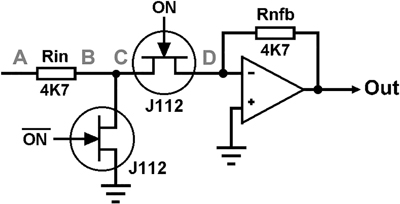
The offness of this circuit is extremely good providing certain precautions are taken in the physical layout. In Figure 21.36, there are two possible crosstalk paths that can damage the offness. The path C-D, through the internal capacitances of the series JFET, is rendered innocuous, as C is connected firmly to ground by the shunt JFET. However, point A is still alive with full amplitude signal, and it is the stray capacitance from A to D that defines the offness at high frequencies.
Given the finite physical size of Rin it is often necessary to extend the PCB track B-C to get A far enough from D. This is no problem if done with caution. Remember that the track B-C is at virtual earth when the mute bloc is on and so is vulnerable to capacitative crosstalk from other signals straying into the area.
Dealing With the DC Conditions
The circuits shown so far have been stripped down to their bare essentials to get the basic principles across. In reality, things are (surprise) a little more complicated. Opamps have non-zero offset and bias voltages and currents, and if not handled properly, these will lead to thumps and bangs. There are several issues:
- If there is any DC voltage at all passed on from the previous stage, this will be interrupted along with the signal, causing a click or thump. The foolproof answer is of course a DC blocking capacitor, but if you are aiming to remove all capacitors from the signal path, you may have a problem. DC servos can partly make up the lack, but since they are based on opamp integrators, they are no more accurate than the opamp, while DC blocking is foolproof.
- The offset voltage of the mute bloc opamp. If the noise gain is changed when the mute operates (which it is), the changing amplification of this offset will change the DC level at the output. The answer is shown in Figure 21.36. The shunt FET is connected to ground via a blocking capacitor to prevent gain changes. This capacitor does not count as “being in the signal path”, as audio only goes through it when the circuit is muted. Feedback of the opamp offset voltage to this capacitor via the 47 kΩ resistor renders it innocuous.
- The input bias and offset currents of the opamp. These are much more of a problem and are best dealt with by using JFET opamps such as TL072 or OPA2134, where the bias and offset currents are negligible at normal equipment temperatures. All of the distortion measurements in this chapter were made with TL072 opamps in place.
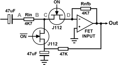
Figure 21.36 Circuit of JFET mute showing stray capacitances and DC handling.
A Soft Changeover Circuit
This circuit (Figure 21.37) is designed to give a soft changeover between two inputs –in effect a fast crossfade. It is the same mute block but with two separate inputs, either or both of which can be switched on. The performance at +20 dBu in/out is summarised in Table 21.7.
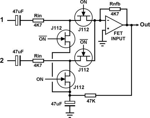
The THD increase at 20 kHz is due to the use of a TL072 as the opamp. J112 JFETs are used in all positions.
This circuit is intended for soft-switching applications in which the transition between states is fast enough for a burst of increased distortion to go unnoticed. It is not suitable for generating slow crossfades in applications like disco mixers, as the exact crossfade law is not very predictable.
| 1 kHz | 10 kHz | 20 kHz | |
|---|---|---|---|
| THD +20 dBu | 0.0023% | 0.0027% | 0.0039% |
| Offness | –114 dB | –109 dB | –105 dB |
Control Voltage Feedthrough in JFETS
All discrete FETs have a small capacitance between the gate and the device channel, so changes in the gate voltage will therefore cause a charge to be transferred to the audio path, just as for CMOS analogue gates. As before, slowing down the control voltage change tends to give a thump rather than a click; the same amount of electric charge has been transferred to the audio path, but more slowly. Lowering the circuit impedance reduces the effects of feedthrough, but halving it only reduces the amplitude of transients by 6 dB, and such a reduction is likely to increase distortion.
Reference
[1] Jones, Morgan “Designing Valve Preamps” Electronics World, Mar 1996, p 193