CHAPTER 26
Interfacing With the Digital Domain
The advance of digital audio has greatly improved the fidelity of audio storage media and generally made wonderful things possible, but sound waves remain stubbornly analogue, and so conversion from analogue to digital and vice-versa is very necessary. Today’s analogue-to-digital converters (ADCs) and digital-to-analogue converters (DACs) have excellent performance, with 24-bit accuracy at a 192 kHz sampling rate a commonplace, but to achieve this potential performance in an application, a good number of factors need to be appreciated. Some of them, such as the need for effective HF decoupling, are relatively straightforward providing you follow the manufacturer’s recommendations, but others, involving the actual interfacing to the analogue input and output pins, are a bit more subtle.
Having said that, contemporary ADCs and DACs are far easier to apply than their ancestors. Oversampling technology means that it is no longer necessary to put a ninth-order brickwall low-pass anti-aliasing filter in front of an ADC or to place a ninth-order brickwall low-pass reconstruction filter after a DAC. If you’ve ever tried to design a ninth-order filter to a price, you will know that this is a very significant freedom. It has had a major effect in reducing the price of digital equipment, particularly in applications like digital mixers, where a large number of ADCs and DACs are required.
ADC and DAC technology moves rapidly; the device examples I have chosen here (2009) will probably soon be out of date. The general principles I give should be more enduring and will be valid for the foreseeable development of the technologies.
PCB Layout Considerations
The PCB layout for both ADCs and DACs requires observance of certain precautions, which are basically the same for both functions. A double-sided PCB is necessary not only because of the large number of connections that have to be made in a small space but also because it allows tracks that need to be isolated from each other to be put on opposite sides of the board. A most important consideration is to keep digital signals, particularly fast ones such as clocks, out of the analogue inputs, so use as much physical spacing between these as possible. Critical tracks on opposite sides of the board should be run at right angles to each other to minimise coupling through the PCB. Do not run digital tracks topside under the IC, as they may couple noise directly into the die from underneath.
Separate analogue and digital ground planes should be used. Most conversion ICs have their analogue and digital interfaces at opposite ends or opposite sides of the package, facilitating the use of separate ground planes. It is usually best to run the analogue ground plane under the IC to minimise the coupling of digital noise. The two ground planes must of course be connected together at some point, and this should be implemented by a single junction close to the IC. Some manufacturers (e.g. Analog Devices) recommend that the junction should be made through a ferrite bead to filter out high RF frequencies. A maximum-copper (minimum-etch) PCB layout technique is generally the best for ground planes, as it gives the most screening possible.
The power supply tracks to the IC should be as wide as possible to give low impedance paths and reduce the voltage effects of current glitches on the power supply lines. Ideally a four-layer PCB (and such boards are now cheaper than they have ever been) should be used so that two layers can be devoted to power supply planes.
Thorough decoupling is always important when using high-speed devices such as ADCs and DACs. All analogue and digital supplies should be decoupled to analogue ground and digital ground, respectively, using 0.1 μF ceramic capacitors in parallel with 10 μF electrolytic capacitors. Some manufacturers recommend using tantalum capacitors for this. To achieve the best possible decoupling, the capacitors should be placed as physically close to the IC as possible and solidly connected to the relevant ground plane.
When you are designing ADCs or DACs into a system, my experience is that significant time can be saved by doing preliminary testing on manufacturers’ evaluation boards; this has particular force when you are using parts from a range you have not used before. Higher Authority may urge you to go straight to a PCB layout, but unless you are very sure what you are doing –if, for example, you are cutting and pasting from an existing satisfactory design –it is a relatively high-risk approach. Evaluation boards are usually expensive, as they are produced in small quantities, but in my view, it is money very well spent.
Nominal Levels and ADCs
The best use of the dynamic range of an ADC is only possible if it is presented with a signal of roughly the right amplitude. Too low a level degrades the signal-to-noise ratio as the top bits are not used, and too high a level will not only cause unpleasant-sounding digital clipping but can cause damage to the ADC if current flows are not limited. Analogue circuitry is therefore needed to scale the signal to the right amplitude.
A typical application of ADCs is in digital mixing consoles. These must accept both microphone and line input levels. Since the signal level from a microphone may be very low (lute music) or very high (microphone in the kickdrum), an input amplifier with a wide variable gain range is required, typically 70 dB and sometimes as much as 80 dB. The signal level range of line signals is less but still requires a gain range of some 30 dB to cope with all conditions. It is therefore necessary for the operator to adjust the input gain by reference to a level meter, so that good use is made of the available dynamic range without risking clipping. In live situations with unpredictable levels, this is always something of a judgement call.
The signal level required at the ADC input to give maximum output, which is usually referred to as full-scale (FS), varies from manufacturer to manufacturer; this important point is brought out in the next section.
Some Typical ADCs
There are a large number of ADCs on the market, and it is necessary to pick out just a few to look at. You will note that the various parts are actually very similar in their application. The inclusion of a device here does not mean that I am giving it any personal recommendation. All the devices mentioned are capable of 24-bit 192 kHz operation. In some cases, the input voltage required for FS appears to exceed the supply voltage. This is not so; the quoted peak-to-peak voltage is the difference between two differential input pins. And now in alphabetical order:
The Analog Devices AD1871 is a stereo audio ADC with two 24-bit conversion channels each giving 105 dB of dynamic range, and each having a programmable gain amplifier (PGA) at the front end, a multi-bit sigma-delta modulator, and decimation filters. The digital details are rather outside our scope here and will not be alluded to further. The PGA has five gain settings ranging from 0 dB to 12 dB in 3 dB steps. The differential input required for full-scale is 2.828 V pk-pk, and the input impedance is 8 kΩ. Like most of its kind, the AD1871 runs its analogue section from +5 V but the digital section from +3.3 V to save power. This IC is unusual in that it is permissible to run the digital section from +5 V, which can save you a regulator.
The Analog Devices AD1974 is a quad ADC with four differential analogue inputs having a very useful CMRR of 55 dB (typical, at both 1 kHz and 20 kHz). These inputs are not buffered and require special interfacing that will be described later. A differential input of 5.4 V pk-pk is needed for FS; the input impedance is 8 kΩ. This IC runs from +3.3 V only.
The Burr-Brown PCM1802 is a stereo ADC with single-ended analogue voltage inputs with input buffer amplifiers. It requires 3.0 V pk-pk to reach full-scale and has a resistive input impedance of 20 kΩ. The analogue section is powered from +5 V, the digital section from +3.3 V.
The Wolfson WM8782 is a stereo ADC with two single-ended analogue inputs with buffer amplifiers. It requires 2.82 V pk-pk (1.0 Vrms) to reach FS, and the input impedance is 10 kΩ. The analogue section is powered from +5 V and the digital core from +3.3 V.
Interfacing With ADC Inputs
The issues involved in interfacing with an ADC depend very much on how the ADC input is configured. As we saw in the previous section, some ADCs, such as the Burr-Brown PCM1802 and the Wolfson WM8782, have internal buffer amplifiers that present a relatively high impedance to the outside world (in this case, 20 kΩ and 10 kΩ, respectively). These inputs are very straightforward to drive. Such buffers are usually only found in ADCs made in a bipolar or BiCMOS process, as making good low-noise, low-distortion amplifiers in a straight CMOS technology is very difficult.
Others, such as the AD1974, do not have buffering and must be driven from special circuitry. In the case of the AD1974 and similar devices, the differential inputs must be driven from a differential signal source to get the best performance. The basic principle is shown in Figure 26.1. The input pins connect to switched internal capacitors, and these generate glitches. Each input pin must be isolated from the opamp driving it by an external series resistor R5, R6 together with a capacitor C5, C6 connected from input to ground. This capacitor must not generate non-linearity when the voltage across it changes, so ceramic NPO or a polypropylene film type must be used.; recommended values for the resistors and capacitors are usually given in the application notes. Note that since the external opamps are referenced to ground, and the ADC internals are referenced to half the +5 V rail, blocking capacitors C2, C3 are needed.
Adding external resistance will slow down the charging of input sampling capacitors. These must be allowed to charge for many time-constants if they are to get close enough to the final value to avoid degrading the performance. External resistance increases the time-constant and can degrade accuracy; manufacturers usually provide guidance as to how much external resistance is permissible for a given number of bits of accuracy.
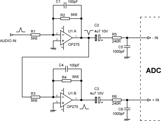
Figure 26.1 A typical drive circuit for an unbuffered differential ADC input.
A point that is obvious but easily overlooked is that the inputs must not be driven to excessive levels. This usually means that the input voltage should not go outside the supply rails by more than 300 mV; for example, Wolfson specifies this restriction for both the analogue and digital inputs of the WM8782 stereo ADC, and the other manufacturers quote similar ratings.
While ADC inputs invariably have clamp diodes for ESD protection that are intended to prevent the inputs moving outside the supply rails, these are small-dimensioned devices that may be destroyed by the output current capability of an opamp. This is why the input voltage should not go outside the supply rails by more than 300 mV –this voltage will not cause a silicon diode to conduct significantly, even at elevated temperatures. The diodes can usually handle 5 mA, but to subject them to anything more is to live dangerously. Obviously the manufacturer’s absolute maximum ratings should be followed on this point, but not all manufacturers give a current rating for their clamp diodes.
Bulletproof protection against input over-voltages is given by running the driving opamp from the same supply rails as the analogue section of the ADC, the opamp saturation voltages ensuring that the input can never reach the supply rails, never mind exceed them. This does, however, restrict your choice of opamp to types that are happy working on low supply voltages; these are likely to be more expensive than the popular audio opamps such as the 5534/5532, which will not give good performance from such low rails. See Chapter 5 for a survey of low-voltage opamps.
If you want to stick with the usual audio opamps, working from higher supply rails than the ADC, then an effective means of protection is the use of external clamping diodes, which, in conjunction with a series resistance, will limit the voltage swing at the ADC input. The principle is shown in Figure 26.2; if the opamp output exceeds +5 V, then D1 will conduct, while if it goes negative of 0 V, D2 will conduct, safely clamping the ADC input.

A vital point here is that the clamp diodes must be of the Schottky type, so their forward voltage is substantially less than that of the conventional silicon diodes on-chip, for otherwise they will give little or no protection. The on-chip diodes will be warmer and would conduct before conventional external silicon diodes.
R1 must be large enough to limit the current in D1, D2 to safe levels but not so large that it causes a roll-off with the ADC input capacitance. It must also not be so large that the non-linear capacitance of the diodes causes significant non-linearity; 1 kΩ should be safe in this respect. Note that R1 is also useful in isolating the opamp output from the ADC input capacitance, which can otherwise erode stability margins.
Some Typical DACs
Unlike ADCs, DACs come in two different types: voltage output and current output. Both types of output require some kind of low-pass filtering, but current output DACs also need current-to-voltage (I-V) conversion stages. There are a large number of DACs on the market, and it is essential to be selective in examining a few typical devices. Once again, the inclusion of a device here does not mean that I am giving it my personal recommendation. All the devices mentioned here are capable of 24-bit operation. And now in alphabetical order:
The Analog Devices AD1854 is a stereo audio DAC delivering 113 dB Dynamic Range and 112 dB SNR (A-weighted) at a 48 kHz sample rate. Maximum sample rate is 96 kHz. Differential analogue voltage outputs give a maximum output of 5.6 V pk-pk at full-scale, and the output impedance is less than 200 Ω. It operates from a single +5 V supply rail, though there are separate supply pins for the analogue and digital sections.
The Texas PCM1794A is a stereo audio DAC supporting sample rates up to 192 kHz. It has differential analogue current outputs giving a maximum of 7.8 mA pk-pk at full-scale. The analogue section is powered from +5 V, the digital section from +3.3 V.
The Wolfson WM8740 is a stereo audio DAC supporting word lengths from 16 to 24 bits and sample rates up to 192 kHz. Differential analogue voltage outputs give a maximum output of 2.82 V pk-pk at full-scale. It can operate from a single +5 V supply rail, or the digital section can be run from +3.3 V to reduce power consumption.
Interfacing With DAC Outputs
Modern DACs use oversampling so that brickwall reconstruction filters are not necessary at the analogue outputs. Nonetheless, some low-pass filtering is essential to remove high-frequency components that could cause trouble downstream from the output.
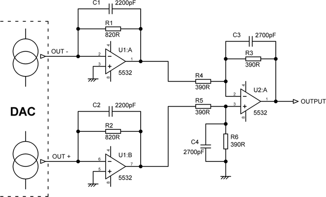
If you are using a DAC with a current output, the first thing you have to do is convert that current to a voltage. This is usually done with a shunt-feedback stage, as shown in Figure 26.3, frequently called an I-V converter. The opamp most popular for this job (and in fact explicitly recommended for the Texas PCM1794A) is no less than our old friend the 5534/5532. The filter capacitors C1, C2 keep down the slew rate required at the outputs of the I-V converters and, with their parallel resistors, give a -3 dB roll-off at 88.2 kHz. The current output is simply scaled by the value of R1, R2 and results in a voltage output of 3.20 V peak for 3.9 mA peak out (half of the total 7.8 mA pk-pk FS output), and when the two anti-phase voltages are combined in the differential amplifier that follows, the total output is 6.4 V peak or 4.5 Vrms. The differential amplifier has its own HF roll-off at 151 kHz to give further filtering, implemented by C3 and C4. The capacitors used must be linear; NP0 ceramic, polystyrene, or polypropylene are the only types suitable.
Voltage output DACs are somewhat simpler to apply, as there is no need for I-V converters and the outputs can drive an active low-pass filter directly. The output is usually differential to obtain enough voltage-swing capability within the limited supply voltage available, so differential-to-single-ended conversion is still required, and this is often cunningly implemented in the form of a differential low-pass filter.
Figure 26.4 shows a typical differential low-pass filter system; it has a third-order Bessel characteristic with a corner frequency of 92 kHz. The outputs are combined, and the first two poles are implemented by the differential multiple-feedback filter around U1:A, and the third pole is produced by the passive network R7, C5. Note that the circuitry uses E96 resistor values in order to obtain the desired accuracy. Multiple-feedback filters are often preferred for this kind of application because they do not suffer from the failure of attenuation at very high frequencies that afflicts Sallen and Key filters due to the inability of the opamp to maintain a low impedance at its output when its open-loop gain, and hence its feedback factor, has fallen to a low value.

Figure 26.4 A typical output stage for a voltage-output DAC, with a differential output filter.
It must not be assumed from this that all DACs have differential outputs. For example, the Wolfson WM8726, described as a “low-cost stereo DAC”, has single-ended voltage outputs; it is recommended they are followed by a second-order low-pass filter.
Interfacing With Microcontrollers
Having looked at interfacing with ADCs and DACs in digital audio, we turn to the important business of interfacing with microcontrollers. Much audio equipment keeps the signals wholly in the analogue domain but uses a microcontroller to handle humble but essential housekeeping tasks such as muting relay control at power-up and power-down and input select relay control. Volume control ICs keep the signal analogue but are controlled by serial data, generated when the microcontroller is driven from a rotary encoder connected to the volume knob. Input select ICs (an array of high-voltage analogue gates) such as the Toshiba TC9163 likewise require serial data to control them. Many pieces of equipment have remote controls, so a microcontroller is essential to decode the incoming RC5 data and activate the correct bit of circuitry. LCD displays typically also take serial data, and with a large display, the software can get complex. The microcontroller will also take the unit out of standby when a 12 V trigger is received.
PIC devices are very popular, and the 16F72 is used as an example here. There are many other microcontroller families; the same basic principles apply. The 16F72 is a capable but inexpensive device that incorporates flash program memory, timers, serial ports, and an 8-bit A/D converter, but here the three 8-bit I/O ports A, B, and C are used to illustrate a preamplifier application. Each port pin can be separately defined to be an input or an output.
Figure 26.5 is not a typical system but illustrates various techniques. The PIC output ports can drive LEDs directly, such as D5 with resistor R2, to set the current. LEDs D1 to D4 indicate which preamp input is selected, and since only one is ever on at a time, they can share resistor R1. For loads such as relays that take more current than an output port can handle directly, a transistor Q1 can be used. Note the suppression diode across the relay coil.
The BA6218 control IC for the motorised volume control is driven by the two output pins RC4 and RC5. These are simple logic outputs and not a serial connection. See Chapter 13 for more on motorised volume controls.
Remote control commands are demodulated and filtered by the IR receiver U3, and the serial data output is applied to RC6. The IR commands are then decoded by software in the PIC.
The B port has a useful extra option. It can be set so that each pin has a “weak pullup” of 250 μA to the +5 V rail; this means that user-operated switches like SW1 do not need an external pullup resistor. When there are a large number of switches to be read, a row-and-column matrix is much more economical of input pins.
The PIC clock frequency is set by ceramic resonator CER1. These components are much cheaper than quartz crystals, and their 0.5% frequency tolerance (crystals show 0.001%) is more than good enough for setting turn-on delays and so on.
Input port voltages must be clamped to ensure they do not exceed the permissible limits. The PIC has protective clamp diodes on all pins, but these have a limited current capability, and if you plan to use them for clamping as opposed to just static protection, a series resistor of around 47 kΩ is recommended, such as R5 on the MAINS FAIL input.
It is an important principle of interfacing that you should not rely on a low at an output port to prevent, say, the mute relay, from energising, perhaps by diverting the drive away from the base of the relay-control transistor. At power-up, the output ports will be at high impedance. This is sometimes referred to as being “tri-stated”, as the high-impedance state is neither the high state nor the low state but a third “off” state. There may be momentary closure of the relay if it operates faster than the microcontroller can initialise itself and write a low to the output port.
More seriously, at power-down, a mute relay must open as quickly as possible to prevent thumps, and it must stay off. The mains-fail circuitry will detect power-down and signal this to the microcontroller, which will write a low to the output port to open the relay. But … the output ports will go high impedance when the microcontroller supply falls. Relays have a wide operating voltage range, so the mute relay will close again, letting through all sorts of unpleasant disturbances, and will not finally open until the supply drops below the hold-on voltage, which may take some time. This is a much more likely scenario than misoperation at switch-on.
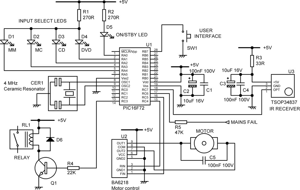
Figure 26.5 Examples of interfacing to a PIC 16F72 microcontroller for preamp housekeeping.
Avoid configuring things so that either a high or a low on an output port must be asserted to prevent something operating.
Many microcontrollers have a Sleep mode, which can be used to minimise the chance of electrical interference. I have never found it necessary to employ this in a piece of audio equipment; RF from the microcontroller getting into the audio has never been a problem. I do know of a case in which it was done very successfully in an HF communications receiver, where the RF sensitivity is of course very much greater. Be aware that some microcontrollers take a surprisingly long time to come out of Sleep mode. Much the same is true of me.