
Chapter 3
Deposition and Patterning
Technologies 1
3.1. Deposition method
Many deposition techniques have been developed for the realization of thin films. Among them there is sputtering under different variants (direct current (DC), radio frequency (RF) magnetron or not, assisted by ion beam etc.) and pulsed laser ablation for physical depositions, the sol–gel process and metal–organic chemical vapor deposition (MOCVD) for chemical depositions. These different deposition techniques are described in this chapter.
3.1.1. Cathodic sputtering
As highlighted by Grove in 1852, cathodic sputtering is a deposition process by which the material to be deposited is ejected from the surface of a solid (target) bombarded by energetic particles [GRO 52]. An inert gas is introduced into the chamber previously degassed under high vacuum (~10−6 mbar). Argon is the most commonly used inert gas. However, it is possible to add oxygen or nitrogen to make reactive sputtering. Under the effect of a DC voltage, there is an electric discharge and stable plasma is then established. The positive ions of Argon (Ar+) are extracted from this plasma under the action of an electric field, and bombard the target raised to the cathode potential. Thus, particles or agglomerates of particles are ejected, which will then be deposited on the substrate placed at the anode potential (Figure 3.1). The physical mechanisms of sputtering have been widely studied and are reported in numerous works [MCC 91].
Figure 3.1. Schematic diagram of cathodic sputtering
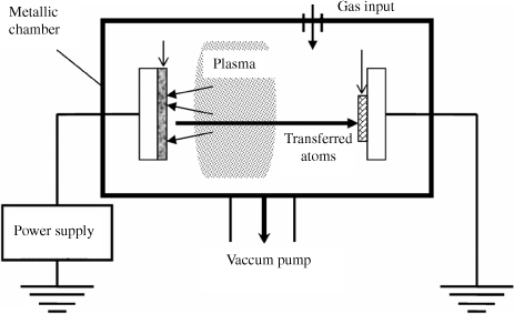
The target can be polarized negatively by either a DC source or an alternating current (AC) through an RF source. In the first case, we talk about DC diode cathodic sputtering because the cathode is connected to the negative terminal of a DC voltage supply. It is only used for metallic target sputtering. In fact, the DC cathodic sputtering of an insulating target is not possible because the surface of the target will be charged with Ar+ ions after a certain time. These Ar+ ions, trapped in the target surface, will repel the incident ions and sputtering will no longer take place. Moreover, it is the oldest deposition process. Although it is still used today due to simplicity of implementation, it tends to be abandoned in favor of the RF cathodic sputtering, which allows both sputtering of an insulating target and achievement of a better performance of sputtering. In this second case, the discharge (plasma), obtained by using a radiofrequency generator (13.56 MHz), is applied to the cathode through an impedance matching circuit that consists of variable capacitors and an inductance. This circuit allows the maximum power transfer to the target by minimizing the reflected power. The anode, which is in front of the cathode, is connected to the ground. At such a frequency, the ions cannot follow the electric field variations (due to their high mass), and the atoms are insensitive to them. Only the electrons can follow the field variations. If the target is insulating, a self-polarization of the system occurs because the target surface becomes negative (through electron accumulation). Unlike the case of DC sputtering, the ions will continue to be accelerated and insulating material sputtering will be maintained. If the target is metallic, it is essential to be able to accumulate the negative charges at the metal surface. This is achieved by a blocking capacitor placed in series with the target to allow the accumulation of electrons on the target. Finally, the use of a magnetron (magnet placed behind the target) can increase the deposition rates and lower the sputtering pressures. In fact, the magnetic field produced by the magnet bends the trajectories of those electrons that are near the target, that is at the plasma level. The increase in the deposition rate that results is due to the increase of the collision probability between the electrons and the argon atoms, thus generating a greater number of argon ions.
In the case of aluminum nitride, the most popular deposition method is pulsed DC reactive sputtering. The gas is a mixture of nitrogen and argon and the target is made entirely of aluminum. During the plasma discharge, a nitriding of the aluminum target surface occurs. This gradually allows target insulation during the deposition. To avoid a pause in sputtering due to a fall in the resultant acceleration voltage, the sputtering DC voltage is regularly reversed to discharge the target surface. The sputtering cycle can then be resumed. Experience shows that for AlN, this method is the most effective. Sometimes, an AC voltage of smaller amplitude is applied to the substrate to re-sputter what has been deposited. This enables us to densify the deposition and adjust the stress on the final layer. This voltage is often referred to as “bias”.
The deposition of complex oxides such as Pb(Zr,Ti)O3 (PZT) is usually done from a ceramic target (single target mode). However, it is possible to achieve a deposition from metal targets (multitarget mode) [VIL 03]. In this configuration, the substrate holder is rotating. Thus, the substrate regularly passes (at adjustable speed) through each of the metal targets, namely Pb, Zr, and Ti. The depositions are then carried out in the RF regime under a gaseous mixture of argon and oxygen. Oxygen reacts with each of the metal components to form the corresponding oxides, that is PbO, ZrO2, and TiO2 in the case of PZT. The major advantage of the multitarget mode is that the bias voltages of each target can be adjusted and the film composition (Zr/Ti ratio, compensation of Pb losses) can thus be controlled. From this point of view, the use of the multitarget mode is more flexible than the single target mode.
The transfer of the composition from the target to the substrate is one of the crucial issues of the cathodic sputtering of PZT due to the high volatility of lead at high temperature, especially in an oxygen atmosphere. In fact, to achieve an in situ growth of PZT films, the substrate is heated. Furthermore, in situ deposition usually provides a film that is more dense than if the deposition is carried out at room temperature [FUJ 07]. For compatibility with the temperature used in the manufacturing processes of circuits on silicon, the temperature is deliberately limited to 550–600°C. To obtain the desired composition, and in particular a Pb/(Zr + Ti) ratio equal to 1, it is appropriate to control the total pressure in the chamber, the partial pressures of argon and oxygen, the distance between the electrodes, as well as the deposition temperature. In a single target mode, there are different solutions to compensate for the lead losses in the film: lead enrichment of the target, the increase of the total pressure, or the decrease of the partial pressure of oxygen. The advantage of the multitarget sputtering mode is that a small increase in the RF power applied to the lead target enables us to compensate for its volatile behavior.
Finally, it should be noted that the parameters are interdependent and that, to some extent, the variation effect of one of them can be partially corrected by modifying another. For instance, a loss of stoichiometry due to an increase in temperature may be compensated by a decrease in the distance between the electrodes or by an increase in the total pressure of deposition.
3.1.2. Ion beam sputtering
Ion beam sputtering (IBS) is a deposition method derived from cathodic sputtering. The IBS principle is illustrated in Figure 3.2. Argon ions generated by an ion gun are projected onto the target after having been previously brought back to their neutral form through a neutralizer.
Figure 3.2. Schematic diagram of the IBS
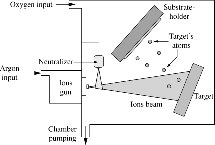
In fact, to avoid the charge issue of the target, the ions are neutralized at the entrance of the deposition chamber by the electrons emitted from the neutralizer. The collision of argon atoms with the target pulls out the elements from the latter, which are deposited on the substrate. A reactive gas, such as oxygen, can be introduced into the deposition chamber to ensure good oxidation in the deposited layer as well as good stoichiometry of the compound.
The IBS technique provides several advantages over the previously described RF sputtering. First of all, it does not induce charging of the target because the incident species are atoms and not ions. Moreover, since the plasma is not in the deposition chamber, the probability of collisions between the target species is highly reduced. The mean free path of atoms is then increased, and the purity of the deposition is improved. In addition, it is a technique for controlling the ion energy very accurately, through independent parameters, including the accelerating voltage and ion beam intensity. Finally, IBS offers the possibility of lowering the crystallization temperature of films compared to other sputtering methods. Thus, Defaÿ et al. have demonstrated the lowering of the crystallization temperature of the STO by using this technique [DEF 02]. More recently, Zhu et al. have reported the manufacture of thin films of BST at 450°C [ZHU 10]. However, IBS exhibits two major drawbacks. The first is that the deposited layers have very high residual stresses that can quickly reach the GPa. The second drawback is the low deposition rate (typically 3 nm/min).
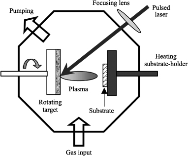
3.1.3. Pulsed laser deposition
The first deposition through laser ablation was carried out by Smith and Turner in 1965, shortly after the appearance of lasers. However, given the low energy density of lasers in that period, the number of deposited materials remained limited. This deposition technique became successful, thanks to the development of short-pulse and very high energy density lasers. The achievement of high-temperature superconducting thin films of YBa2Cu3O7 by Dijkkamp and Venkatesan in 1987 contributed to the notoriety and dissemination of pulsed laser ablation in the scientific community. Since then, it is widely used in fundamental research laboratories for the synthesis of very high crystalline oxides films. However, the integration of this deposition technique in the industrial world is currently still not possible because of the inhomogeneity of depositions on large-size substrates (200 mm).
The principle of pulsed laser deposition consists of focusing a high-energy pulsed laser beam onto a rotating target of the material to be deposited. The laser-material interaction leads to the creation of a plasma called plume. The material is ejected perpendicular to the surface of the target and condenses on the substrate. The substrate is generally heated to allow the in situ crystallization of the material (Figure 3.3).
Figure 3.3. Schematic diagram of the pulsed laser ablation
Laser ablation deposition can be described in the following three main steps:
– Laser-target interaction: for a sufficiently high flux density and a relatively short-time pulse (few nanoseconds), laser energy is transmitted to the atoms of the target. The absorbed energy is not dissipated in the material and is thus concentrated within a small volume. It is then redistributed in the material by the coupling of electrons and phonons, which leads to the heating of the material and its evaporation. The instantaneous ablation rate is highly dependent on the fluence (energy per unit area) of the laser.
– The formation and expansion of the plasma: at the ablation threshold, high-density plasma is formed and is composed of ions, atoms, and clusters of atoms. This plasma allows the transfer of atoms or ions from the target to the substrate. The highly directional expansion of the plasma (which takes the form of a feather) is the cause of lack of spatial uniformity of the thickness of the deposited films. The depositions by PLD are most often made in a controlled atmosphere. The higher the pressure in the chamber, the higher is the probability of collision between the elements of the gas and the plasma.
– The growth of the film on the substrate: the atoms or ions projected onto the substrate condense and react with the reactive atmosphere in the chamber, which leads to the growth of the thin layer. The growth of films is a complex phenomenon that depends on several factors, such as density, energy, ionization degree, and type of condensed material as well as temperature and physicochemical properties of the substrate.
The main advantage of this deposition technique is the material ablation mechanism that produces a stoichiometry plasma similar to that of the target. This makes it relatively easy to obtain a multielement film in the same stoichiometric proportions as in the target material. In addition, pulsed laser ablation provides excellent layer-by-layer growth control, thus allowing us to obtain epitaxial films of very high crystalline quality [VRE 06]. Moreover, superlattices can be realized through a change in the target [VRE 07]. However, this technique has two major drawbacks. The first drawback is related to the too small film surface on which it is possible to deposit homogeneously. The second drawback is the presence of very small droplets of material on the surface of the synthesized films. These droplets come directly from the target following the extraction of aggregates under the impact of the laser beam and lead to an increase in the surface roughness of thin films. The density of these particles on the film surface can be reduced by the use of a fully densified target.
3.1.4. The sol–gel process
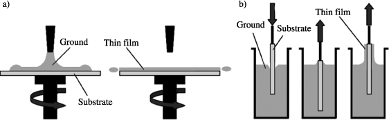
The sol–gel process has been known since 1845 for the synthesis of silica glass. However, it was only a century later that the idea of sol–gel polymerization was adopted by the glass industry. The first “sol–gel” patent was submitted in 1939 by the German firm Schott for the realization of rearview mirrors. The use of sol–gel for the production of piezoelectric thin films is much more recent. The sol–gel deposition of PbTiO3 (PT) was reported for the first time in 1984 by Gurkovich et al. [GUR 84]. The following year, Budd et al. described the synthesis of lead-based perovskite thin films (PT, PbZrO3 (PZ), PZT, (Pb,La)(Zr,Ti)O3 (PLZT)) [BUD 85]. This process uses a solution containing reactive precursors such as the metal salts or the alkoxides and a solvent. The deposition of thin films can be made by spin coating or by dip coating as shown in Figure 3.4.
Figure 3.4. Process of sol–gel on a substrate: (a) by spin coating and (b) by dip coating
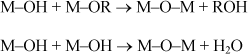
The principle of the sol–gel process is based on a series of reactions of hydrolysis condensation at a temperature close to room temperature, which leads to the formation of an inorganic polymer, which can then be thermally treated. The hydrolysis step of metal alkoxides is represented by the following reaction:
![]()
where M denotes a metal cation and R an alkyl organic group. This reaction allows the conversion of alkoxy functions in hydroxy function. The resulting solution is called sol, which is a solid phase consisting of small entities dispersed in a liquid (the solvent). The hydroxy functions are then converted into the M–O–M species corresponding to the formation of a macromolecular mineral lattice forming the gel. This is carried out by using several condensation reactions (formation of bridges oxo, –O–, through oxolation reactions) with alcohol and water elimination:
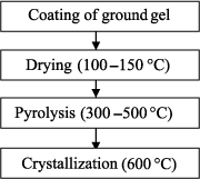
The realization of piezoelectric films through the sol–gel technique consists of a series of steps of coating of the sol–gel solution and of heat treatments, as shown schematically in Figure 3.5. The solution is usually spread over a substrate by spin coating. The thickness of the deposited film depends mainly on the rotational speed of the spinner and the physicochemical parameters of the solution (viscosity, concentration, and evaporation rate). A drying step allows us to evaporate part of the solvents and obtain a solid deposition. The layer is then subjected to pyrolysis (or calcination) to remove the organic residues. This step, usually performed on a hotplate, is crucial because it greatly determines the structural quality of the piezoelectric film. The calcination temperature should be high enough to remove all the organic residues (typically between 300°C and 400°C). Otherwise, the trapping of organic matter can lead to the presence of porosity. However, very high temperature may favor the appearance of the parasite phase, such as the pyrochlore in the case of PZT. Furthermore, it has been shown that the temperature at calcination could influence the crystallographic orientation of PZT films [GON 04]. After pyrolysis, the resulting amorphous layer is crystallized and densified at a temperature that ranges between 600°C and 800°C. This crystallization step is usually carried out through rapid thermal annealing (RTA), rather than through conventional annealing, notably to limit the thermal budget. Nowadays, the RTA process is among the most used for the crystallization of thin films. Its main asset is a transfer of the thermal energy through radiation and not through convection. This results in extremely quick rises in temperature up to 300°C/s through the use of halogen lamps. The annealings last for a few dozen seconds. The thickness of a layer after crystallization is generally about 50 nm. Depending on the final thickness of the desired material, all the earlier described steps should be repeated several times. However, the crystallization step is very often carried out for every two or three pyrolyzed layers. This explains the interest in using the RTA process to reduce both the thermal budget and the manufacturing time of films.
Figure 3.5. Successive steps of the sol-gel process during the production of piezoelectric films
The deposition technique through sol-gel is still used sparingly in the microelectronics industry, but there are some fine examples of industrial realizations [BOU 05]. In addition, it tends to be increasingly used for the integration of piezoelectric materials in microsystems. Indeed, the best piezoelectric properties of PZT films are obtained for layers produced from sol-gel [CAL 07]. The sol-gel process has the advantage of being inexpensive and relatively simple to implement, requiring only a spin coater, hot plates, and an RTA oven. Moreover, it does not require any maintenance, which is a considerable asset compared to deposition techniques under vacuum. It is also very flexible for the development of complex materials. Thus, the compositions can easily be varied through the dosage of organometallic precursors. The dopants can also be introduced to optimize the film properties. The main disadvantage of this method is the small thickness of a deposited monolayer, which is in the order of 50 nm. Thus, nearly 20 spreading-annealing steps are required to prepare a film of 1 μm thickness. The use of a higher viscosity solution is expected to reduce the number of coatings, but this is usually done at the expense of film properties because it is then more difficult to obtain a sufficiently dense layer.
3.1.5. The MOCVD
The MOCVD consists of chemical vapor deposition (CVD) from organometallic precursors. The principle of CVD is to bring into contact the substrate heated under vacuum, a volatile compound of the material to be deposited. The different steps of the deposition are illustrated in Figure 3.6. The precursors are conveyed toward the substrate by the carrier gas (argon and nitrogen), and then they are adsorbed on the substrate surface. The reactive species diffuse on the surface up to the preferential sites and react in a heterogeneous phase to give rise to the formation of the film. The volatile by-products of the reaction are discharged through the stream of the carrier gas.
Figure 3.6. Principle of deposition through CVD
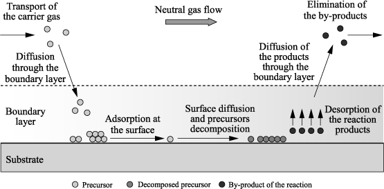
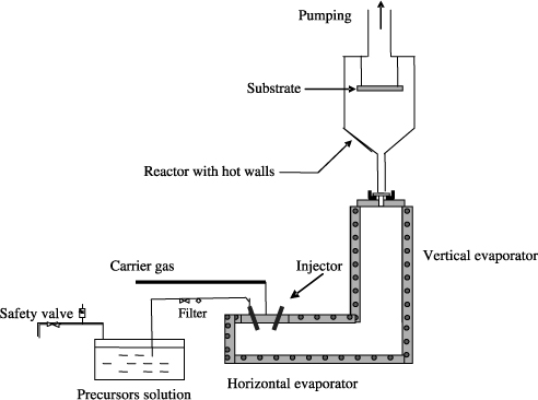
Figure 3.7 shows a simplified diagram of an equipment of deposition through MOCVD with direct liquid injection. The use of an injector allows sending of droplets of the precursor solution in the pulsed regime in an evaporator. The aerosol thus formed is quickly vaporized in an evaporator. The resulting vapors are conveyed in the deposition chamber through a gas mixture that consists of the neutral carrier gas (N2 or Ar) and a reactive gas. Thereafter, they decompose to form a layer on the substrate. To avoid any premature condensation and/or decomposition of the precursors, an increasing gradient of temperature is set between the evaporator and the deposition chamber. The hot walls of the reactor also allow us to avoid vapor condensation. In the case of a solution that contains several organometallic precursors, the evaporation temperature is selected from the precursor that volatilizes at the highest temperature. The growth speed can be controlled according to the time of opening of the injector, the injection frequency, and the concentration of the solution. The critical parameters of the MOCVD are pressure, gases used, and especially the temperatures of the evaporators and the substrate.
MOCVD is very attractive for its large coating power, which enables us to notably fill the trenches for 3D applications, its high deposition speed (up to 100 nm/min), and good control of the stoichiometry of the films [SAK 91]. The major drawback of this technique is the complexity of the implementation, because of the reaction mechanisms. The stability of the precursors is furthermore difficult to control. Finally, the extreme toxicity of the organometallic precursors requires a security system of gas pipes. The cost of such equipment is not negligible.
Figure 3.7. Schematic diagram of MOCVD with direct liquid injection
There are other versions of the CVD technique. Among them, plasma-enhanced CVD (PECVD), low-pressure CVD (LPCVD), and atomic layer CVD (ALCVD) are the most widely known.
3.1.6. Molecular beam epitaxy
The first depositions using the molecular beam epitaxy (MBE) technique were conducted in the late 1950s by Gunther on the III-V system. The latter succeeded in growing stoichiometric thin films of InSb and polycrystalline InAs deposited on glass substrate 10 years later, and Davey and Pankey showed the growth of a monocrystalline thin layer of GaAs on a monocrystalline substrate. Then, in the 1970s the growth mechanisms of III-V materials by MBE were studied by A. Cho and J. Arthur at Bell Laboratories for the crystalline growth of III-V semiconductors.
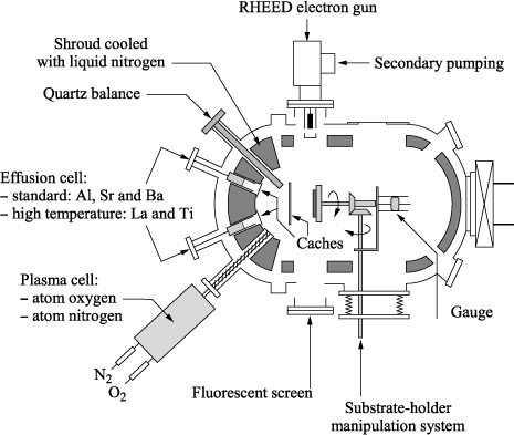
Molecular beam epitaxy allows us to perform under ultra-high vacuum (10−10 to 10−11 Torr) the epitaxial growth of thin layers of semiconductors, metals, or insulators, by reaction between a beam of atoms or molecules and the surface of a substrate. In fact, this technique is based either on the co-evaporation or the sequential evaporation of the elementary constituents. The walls of the growth chamber are cooled with liquid nitrogen and all the particles are then condensed on it, which reduces the pollution inside the chamber and lowers the vacuum level. The advantages of MBE are the ability to perform complex heterostructures with abrupt interfaces and the control of the growth, layer by layer in real time by using in situ reflection high-energy electron diffraction (RHEED; diffraction of high-energy electrons in the grazing incidence on the surface of the crystal in formation).
The typical growth speeds, often less than the monolayer per second (ML/s), are slow enough to ensure a diffusion of species on the surface of the substrate, which enables us to obtain low roughness surfaces. MBE growth is carried out far from the thermodynamic equilibrium. It is mainly governed by the kinetics of the growth processes between the superficial atomic layers of the substrate and the atoms of the incident flux. This is a difference compared to other deposition techniques where the species arrive on the substrate surface with a lot more kinetic energy.
To evaporate the elements, two techniques are used: an electron gun or Knudsen-type effusion cells. With the first technique, the material sources are commonly binary oxides that evaporate congruently (by keeping the stoichiometry), such as MgO, Al2O3, or Gd2O3. Evaporation through the electron gun is also used in the case of metals whose melting point is too high to use the Knudsen cells whose maximum operating temperature is 2,000°C. With the second technique that uses the effusion cells, metals (whose melting point is lower than 2,000°C) such as barium, titanium, strontium, and germanium are evaporated separately because of their different vapor pressures for forming a stream of atomic or molecular beams with a separate oxidation source. It is necessary to properly control the flow of each source to obtain the correct stoichiometry in the film. The evaporated species are then adsorbed on the surface of a monocrystalline substrate heated to promote epitaxy of a monocrystalline film.
The streams resulting from the cells are molecular beams according to the kinetic theory of gases: the mean free path of the evaporated elements is very large compared to the source – sample distance. This is the regime of the Knudsen molecular effusion limiting the interaction between the evaporated atoms. The interposition of a cache between each cell and the substrate is used to interrupt the element streams and stop the growth very quickly. As a result, two types of growth can be envisaged for the implementation of complex composition oxides (e.g. ternary oxides). Either the caches are simultaneously opened and the elements are deposited on the surface at the same time, or the caches are alternatively opened leading to the deposition of a series of differentatomic planes. In this case, this is alternate MBE. This technique allows control of the growth layer by layer or sublayer by sublayer and creation of new multilayer compounds. Different oxidation sources can be used: molecular oxygen, atomic oxygen, ozone, or nitrogen dioxide. The deposition of films through evaporation is limited to a pressure of less than 10−4 Torr in order to not reduce too heavily the mean free path of the evaporated species down to the substrate. For many oxide materials, this molecular oxygen pressure is not sufficient to either obtain the correct desired phase or the oxygen stoichiometry. It would be necessary to produce depositions with higher molecular oxygen pressure. The solution to this problem is to use a species that is more reactive than molecular oxygen, such as nitrogen dioxide (NO2), ozone (O3), or even atomic oxygen (O). The latter compound is produced by separating a molecule of O2 in a chamber of radiofrequency plasma. It is also possible to form in situ atomic oxygen or ozone from molecular oxygen by irradiating the film during deposition through ultraviolet (UV) rays. The UV photons produce species (O and O3) in excited states, which increases their reactivity considerably.
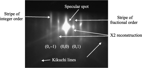
Diffraction at the grazing incidence of the reflected electrons (RHEED) is a technique used in MBE to characterize growth in real time. Indeed, the low deposition pressure in the growth chamber allows the use of an electron beam throughout electron beam epitaxy. In 1983 Neave and Van Hove showed the advantage of using the RHEED oscillations during crystal growth to precisely control the thickness of thin films and superlattices of semiconductors. In addition, it was possible to collect valuable information in situ, notably on surface reconstructions and growth kinetics. Finally, the shape of the diffraction spots (stripes or spots) as well as the quality of the diffraction diagram (clear or diffuse spots) provided information on the crystallinity of the layer and its surface and roughness quality.
An electron beam accelerated at voltages from 10 kV to 100 kV (its associated wavelength then ranges between 0.04 Å and 0.15 Å) allows probing the matter at the atomic scale through the diffraction diagram. As the mean free path of the electrons in the solid is a hundred angstroms, the low incidence angle (between 1° and 3°) allows us to probe only a few monolayers and thus collect information that is related only to the surface of the material.
The incident electrons and those that are diffracted by the surface are then detected by a fluorescent screen perpendicular to the plane of the sample. In the framework of the kinematic theory (elastic scattering of electrons), the diffraction diagrams observed on the screen correspond to the intersection of the reciprocal lattice of the surface with the Ewald sphere of radius k (k is the modulus of the wave vector of the electrons of the incident beam: k = 2π/λ, λdenotes the wavelength).
Thus, the resulting diffraction pattern allows visualization of the reciprocal lattice of the surface of the sample.
Figure 3.8. Diagram of a deposition frame through molecular beam epitaxy
An atomically flat surface can be modeled by a 2D periodic arrangement of atoms and its reciprocal lattice corresponds to a lattice of rods perpendicular to the surface. The intersection of the Ewald sphere with the lattice of rods should form points. A diagram in the form of rods appears. In fact, in the case of RHEED, there is some instrumental divergence (angular and energy). Thus, a certain spectral width of the beam leads to a thickness of the Ewald sphere. Furthermore, since the crystal is finite, the reciprocal lattice is itself made up of lines of finite width. The diffraction diagram is therefore composed of lines, whose thickness is related to both the monochromaticity of the incident electron beam and the size of single crystals or their imperfections. The presence of reconstructions on the surface plane leads to the presence of additional stripes of fractional order. The central stripe (or specular spot), more intense than the others, corresponds to the beam reflected by the surface; its intensity is related to the density of atomic steps on the surface. Finally, it is possible to observe lines of less intensity called Kikuchi lines resulting from nonelastic collisions of electrons with atoms. These lines appear in the case of a layer having both very good crystallinity and flatness. The shape of the diffraction stripes provides information on the growth mode and the crystalline quality of the layer on the surface. A very smooth 2D surface is characterized by the presence of Laue areas in the diagram, appearing in the form of spots forming arcs. If the surface becomes rough, bright spots appear at the location of Bragg spots. The thinnest of the stripes is relative to the crystalline quality of the layer. The thinner the lines, the better is the crystalline quality. If the diffraction pattern no longer exhibits stripes but diffraction spots, called Bragg spots, growth becomes 3D. If the deposited film is polycrystalline, then diffraction rings appear on the RHEED pattern, analogous to a powder diffraction pattern.
Finally, in the case of an amorphous layer, there will be a simple uniform halo, characteristic of the disappearance of periodicity. The RHEED pattern also provides information on the lattice parameters. In fact, the spacing between the lines (or diffraction spots if growth is 3D) depends on the interplanar distance in the surface plane. The oscillations of the specular spot intensity during a layer-by-layer growth provide us with information on growth mode and speed. The first RHEED oscillations were observed by Harris in 1981 during the GaAs growth. The change in surface morphology alternating between flat layers and intermediate steps that are rougher causes an intensity variation in the diffracted beam. The intensity of the specular spot will then present oscillations, passing through a minimum for a half monolayer and through a maximum for the completion of a monolayer, and this will regularly happen if layer-by-layer growth takes place. The growth rate, as well as the thickness of the deposited film, can thus be accurately determined from the oscillations period, each oscillation corresponding to the deposition of a monolayer.
It should be noted that, in the case of the diffraction of electrons, charge effects can occur with insulating materials such as oxides. The charge accumulation on the surface can turn the method unsuitable and lead to the disappearance of the RHEED diagram. The phenomenon is especially observable when the epitaxies are performed at low temperature.
Figure 3.9. Example of RHEED diffractogram
3.2. Etching
The etching of materials is a vast and crucial subject for integration into a technological process. We will only cover a tiny part of this problem by providing only some basic recipes to etch the considered materials. This area requires a certain technological know-how that it is sometimes difficult to share.
3.2.1. Wet etching
Wet etching of perovskite-type oxides is mostly done with a mixture of HF and HCl acids diluted with water. The amount of water varies according to the crystalline state of the perovskite. In fact, in the amorphous state, for example, after deposition through sputtering at room temperature, the perovskite is much easier to etch than when it is crystallized. A standard dilution is a dose of HF 1%, a dose of HCl and 10 doses of water.
3.2.2. Dry etching
Dry etching of perovskites is quite difficult because the volatile compounds likely to form are few. The best results are obtained by combining purely mechanical etching based on argon (ion milling) with chlorine compounds rather than fluorine compounds. An equally delicate point is the etching of the electrodes, notably IrO2 and Pt. In fact, the latter is particularly stable, which means a dry etching that is almost exclusively based on the mechanical effect of bombardment through ion milling. This leads to the redeposition of metal particles, which can be very penalizing for the remainder of the technology. Ru is easier to etch because some of Ru oxides are in the gaseous state at room temperature. But RuO4 is harmful, which leads to serious safety concerns.
3.3. Contamination
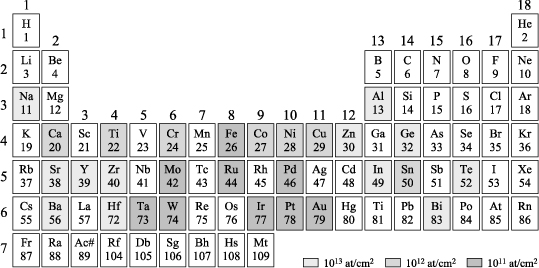
The use of new materials in clean rooms that were originally designed for working on well-known material in microelectronics (Si, SiO2, Al and some doping materials, such as B or P) induces a problem of compatibility of technologies. Indeed, beyond the cleanliness required to prevent dusts that have a typical size of a micron, several materials are killers of semiconductors. Here is an illustration in the classification table of the most dangerous materials for the CMOS devices, derived from a study by Bigot et al. [BIG 05]: Fe, Mo, Ru, Pd, Ta, W, Ir, Pt, and Au. Many of these materials are used in piezoelectric and dielectric applications based on perovksites: Mo as electrodes of AlN, W in the acoustic Bragg mirrors of resonators, Ir, Ru, and Pt as electrodes of PZT, and Au as a very helpful conductive metal in the metallization of RF components.
Figure 3.10. Materials that inhibit semiconductors. The darker the color, the more dangerous the material for the semiconductor
It is therefore essential to develop a drastic strategy to enable the coexistence of semiconductor components with other devices. One possibility may be to completely dedicate clean rooms either to CMOS processes or to microsystems.
3.4. Monocrystalline thin-film transfer
There are two main techniques of thin-film transfer, which enable us to preserve the monocrystalline nature of the initial substrate:
– Smart Cut™ technology [BRU 95] based on gas ions implantation (typically hydrogen) and direct bonding;
– the technique of bonding/thinning.
These are the only techniques that enable us to transfer a monocrystalline layer on to a host substrate. These are perfectly mastered for silicon and enable, among other applications, the industrial production of silicon on insulator (SOI) wafers.
These two techniques differ in the range of material thickness that can be transferred. So, for the SOI, the thickness ranges according to the two techniques shown in Figure 3.11.
Figure 3.11. Possible range of thickness and uniformity with the Smart Cut™ technology and bonding/thinning
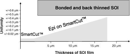
Thus, according to the intended application, any one of the technologies can be used on our substrates based on the piezoelectric material.
3.4.1. Smart Cut™ technology
Smart Cut™ technology was used by M. Bruel at the CEA-LETI in the early 1990s [BRU 95]. Nowadays, it is this technology that allows the realization of SOI substrates in production up to diameters of 300 mm.
Smart Cut™ technology can be broadly summarized through four key steps (see Figure 3.12). The diagram shows and describes the typical steps of development of an SOI substrate.
Hydrogen implantation is performed on a substrate (A) of oxidized Si. The oxide layer is then the future buried insulating film of the SOI structure. This implantation generates the formation of an area weakened in depth, which consists of microcavities whose growth is at the basis of the phenomenon of detachment.
Molecular bonding allows us to fasten the implanted plate (A) on the support plate (plywood or base) (B), which is not necessarily oxidized. Surface preparation is required to obtain a bonding of good quality.
The fracture step is performed in the weakened area through a heat treatment in the range of 400–600°C. This gives, on the one hand, the SOI structure and, on the other, the substrate that is initially implanted (A′) and then peeled off the transferred layer. The latter can then be recycled for the production of another transfer.
Figure 3.12. Main steps of the Smart Cut™ technology applied to the SOI
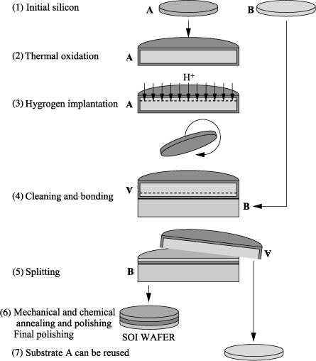
The final treatments consist, on the one hand, of an annealing at high temperatures to strengthen the bonding interface between the transferred thin film and the support substrate and, on the other, of a polishing, that enables us to obtain the desired final surface film thickness of silicon, and to obtain a good surface state.
3.4.2. Bonding/thinning
The bonding/thinning technique as the Smart Cut™ process enables us to obtain the transfer of monocrystalline thin layers. The thickness of the resulting thin films, on the contrary, is much greater, typically between 5 and 10 units. This thickness can also be very interesting for thin layers of LNO in the context of surface acoustic wave (SAW) filters. This technique consists of three main steps as schematized in Figure 3.13.
Figure 3.13. Milestones of the collage-thinning technology
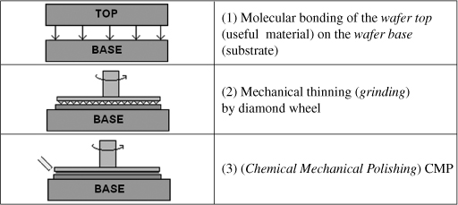
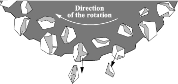
A first bonding step is performed between two materials before thinning of the material from which we want to get the thin film. The bonding is generally made through hydrogen bond interactions in the case of two oxidized plates. The essential step (compared to the Smart Cut™ process) of this technology is mechanical thinning. For this we use a buffing wheel whose active part is a powder of abrasive grains (mostly diamonds). The different wheels are characterized by an index that defines the average size of the abrasive grains according to the following formula: size (in μm) = 16,000/index. This powder is taken in a resin matrix that will release the abrasive grains during the polishing, wear itself, and reveal new abrasive grains: it is a self-sharpening phenomenon, illustrated in Figure 3.14 in the case of a saw (same principle as thinning). This phenomenon allows the polishing wheel to keep its abrasion ability constant throughout its lifetime. From a more general point of view, thinning takes place in several phases: coarse wheel thinning #325, fine wheel thinning #8,000, and surface finish through CMP, which allows reduction of the roughness and obtaining of the desired thin layer thickness while removing the hammer-hardened zone.
Figure 3.14. Principle of self-sharpening of the wheel
3.4.3. Interest in the material in a thin layer
The use of monocrystalline thin films for this type of application is an innovative approach that differs from conventional deposition techniques. Indeed, the fact of transferring a material on a host substrate presents some advantages at various levels:
– Concerning the active layer:
– obtain monocrystalline layers. The expected major gain is the removal of grain, and thus of grain boundaries;
– in the case of a transfer through Smart Cut™, the thickness of the transferred layer is directly related to the implantation energy of the ion beam, and therefore provides good flexibility at the level of thickness combinations (thin film and buried oxide). For example, the transferred thickness of silicon can range from a few tens of nm to about 2 μm by using a conventional implanter (energy <210 keV);
– in the case of a transfer through Smart Cut™, the transferred layers are uniform and homogeneous in thickness because they are defined by an implantation depth and not by mechanical thinning;
– in the case of a transfer through Smart Cut™, manufacturing costs are reduced, on the one hand, by recycling of the substrates (the plates that are initially ion implanted can be reused after the transfer of the thin film), and, on the other, by the use of standard equipment in microelectronics.
– Concerning the support substrate: this is a flexible process that allows the realization of heterostructures. Thus, Smart Cut™ technology allows, for example, combination of the advantages of a solid support substrate of Si (cost, weight, mechanical properties, etc.) and a thin active layer. The transfer of layers of different materials such as SiC [DIC 97], GaAs [JAL 98], InP [JAL 99], GaN [TAU 05], or Ge [DEG 05] is thus possible. These transfers can be performed on different substrates: quartz, Si, Ge, GaAs, sapphire, etc. If, in principle, many combinations are actually possible, the development of any new system, however, systematically requires significant efforts of process adapting.
– Additional layer: this is a process that allows us to consider, at the cost of technology development, the integration of electrodes required for some components.
3.4.4. State of the art of the domain/applications
3.4.4.1. Substrates obtained through transfer of monocrystalline layers
Most studies in the state of the art on this transfer are based on perovskite niobate and lithium tantalate for piezoelectric applications and ferroelectric memories. Regarding the literature on the transfer of piezoelectric materials, we find publications on layer transfer using technologies close to Smart Cut™. We find [LEV 98] a unique example of high-energy implantation (3.8 MeV) for a dose of 5 × 10¹⁶ He+ ions/cm2, which enables us to achieve the transfer of a thick layer of LNO in the order of 9 μm. However, due to the implantation energies used, this technique is difficult to industrialize.
Studies closer to the Smart Cut™ standard conditions in terms of ion implantation are described in the publication [PAR 06]. These authors show the realization of a transfer of 800 nm of LNO through the co-establishment of H+ at 80 keV standard conditions in terms of implantation, which are described in the publication [PAR 06]. These authors show the realization of a transfer of 800 nm of LNO through the co-implantation of 5×10¹⁶ ions/cm2 and an energy of 115 keV helium with a dose of 1017 ions/cm2. The originality of this publication is in the mechanism of transfer that is carried out using a cw-CO2 laser (100 MW/m2) as a source of heat for this purpose.
A study carried out by the team of Alexe [RAD 03] focused on finding the optimum conditions of blistering (determining conditions of a Smart Cut™ transfer) for different materials such as LiNbO3, LaAlO3, SrTiO3, or even of PLZT, using helium and hydrogen ions. Similar studies have been made in the LTO [WAN 01] using H+ and B+/H+ co-implantation; these authors essentially focused on the characterization of the damage created by the implantation and the annealing healing effect.
A recent publication [HUH 09] shows a transfer of LNO through Smart Cut™, with conditions very close to our standards. Optical waveguides (ridge type) are formed, showing propagation losses of the order of 3 dB/cm.
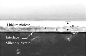
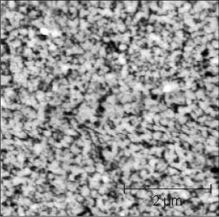
The state of the art about the creation of LNO substrates through bonding/ thinning is much limited. Taiwanese researchers obtained a layer of LNO thinned to 10 μm on a substrate on a silicon substrate through this technique of bonding/thinning [WUC 06]. After bonding, the LNO substrate on Si is first thinned mechanically through arinding up to 40 μm thickness and then, second, the LNO substrate is thinned through CMP with removal speeds of 100 nm/min up to a thickness of 10 μm. A sample of the final substrate is analyzed through SEM on the wafer (Figure 3.15) and shows a certain uniformity of the bonding interface as well as a thickness of LNO of 10 μm. The homogeneity of the LNO layer over the entire silicon substrate is incontestable.
Figure 3.15. SEM image of a sample of LNO thinned on Si through bonding/thinning
3.4.4.2. SAW filters
In 2002, CEA-LETI in collaboration with the Femto laboratory in Besancon developed thin films (between 500 nm and 1 μm) of LNO on Si (100) [PAS 07]. The objective of this study was to develop SAW filters for high frequencies of 1–2 GHz. The filters that were used were conventional SAW filters made of two interdigitated combs (which can be regarded as a transmitting acoustic antenna and a reception antenna), and, by playing on the pitch between the electrodes of the two combs, it was possible to vary the frequency from 1 GHz to 2 GHz. The smaller the pitch between two electrodes, the more important the resonant frequency will be. The coupling coefficients for the Rayleigh waves and the shear waves at both frequencies showed values close to theoretical values. The coupling coefficient in the case of shear waves has doubled, going from 1 GHz to 2 GHz (6% to 12.5%) while it remained virtually unchanged in the case of Rayleigh waves (2% for 1 GHz and 1.3% for 2 GHz). As expected, the coupling coefficients were significantly larger for shear waves than for the Rayleigh waves. Then, the same researchers referred to a p-doped silicon substrate. It has been shown that there was an optimum acoustic coupling coefficient over a wider frequency range.
3.4.4.3. BAW filters
Osugi et al studied the FBAR filters with layers of LNO and LTO [OSU 07]. They have made structures with piezoelectric layer thicknesses between 990 and 1,015 nm. They realized that by varying both the material (LMO or LTO) and its thickness, we vary Δf/fr and therefore the bandwidth. By performing a coupling of two FBAR resonators (with piezoelectric layer thicknesses of 100 nm), they were able to obtain a band-pass filter with a resonant frequency of 2.13 GHz and a bandwidth of 227 MHz, values very close to expected theoretical values. However, the rejection level is very low and therefore the signal-to-noise ratio is also low.
3.4.4.4. Optical applications
The LNO thin films also have applications in the optical domain. A study was performed on waveguides with regions of reversed domains from thin layers of LNO and LiTaO3 (LTO) [YAM 91]. The reversed fields in the case of LNO were obtained by working directly on the film of niobate pads of SiO2 through photolithography. By heating the structure, lithium will diffuse into the studs. We will then obtain electrically reversed regions. The comparison between LNO and LTO at the propagation losses level and conversion efficiency was significant in favor of LTO. In addition, LNO presented optical damage unlike LTO.
3.4.5. An exemplary implementation
3.4.5.1. Technology
The Smart Cut™ technology (as described earlier) was used in the specific case of the LiNbO3-type material. A specific process has thus been developed in terms of metal electrode deposition, implantation and transfer. For simplicity, particularly because the expansion coefficients are anisotropic and high compared to silicon, the LiNbO3-type structures transferred on LiNbO3 were initially studied.
The development of this process allows us to obtain two types of substrates (Figure 3.16).
Figure 3.16. LiNbO3 substrate transferred on oxide layer without (a) with (b) metal layer
3.4.5.2. Substrate characterization
An important point concerning the implementation of these substrates is the preservation of the piezoelectric properties of the material after transfer. The transferred layers were first characterized from a crystallographic point of view. The crystallinity of the transferred layer was characterized by X-ray diffraction.
Figure 3.17 shows the diffraction diagrams of a transferred layer of LiNbO3 and a solid substrate of LiNbO3, centered on the stripe (400).
Figure 3.17. Diffraction diagram of a transferred layer of LiNbO3 and a solid substrate of LiNbO3, stripe (400). Insert: image HTEM exhibiting residual point defects of the implantation
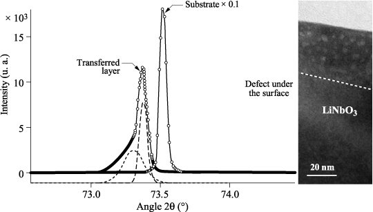
The diffraction diagram of the solid substrate of LiNbO3 is typical of monocrystalline material. The lattice parameter to be extracted, which will be used as a reference, is a = 5,149 Å, against a theoretical value of 51,505 Å, a difference of 0.3‰. The diffraction diagram of the transferred layer of LiNbO3 appears to be slightly shifted toward the higher lattice parameters. Moreover, it has a residual gradient of the lattice parameter, toward the higher lattice parameters that can be decomposed into two peaks with parameters, respectively, from a = 5,157 Å to a = 5,161 Å, which is an increase of +1.7 to 2.5‰ Å compared to the solid substrate. The lower peak in amplitude can be viewed as residual surface defects of the implantation step [SOU 06] and observed in XTEM (Figure 3.17). The higher peak in amplitude corresponds to the rest of the layer whose width at half maximum of the rocking curve, which represents the quality of crystal packing, is similar to that observed on the bulk substrate. This latter observation confirms the monocrystalline nature of the transferred layer.
After the transfer, chemical and mechanical polishing processes can improve the final roughness of the layer. This step also allows us to adjust the final thickness of the layer, which has a direct influence on the frequency of the component. Thus, an observed roughness after polishing of about 10.2 nm RMS measured by AFM (Atomic Force Microscope) on a scan of 5 × 5 μm (Figure 3.18) can be reduced to a roughness of about 0.2 nm for the same scan size. This roughness is then compatible with component manufacturing.
Figure 3.18. AFM image of a surface of LiNbO3 after transfer. The measured roughness for this scan of 5 × 5 μm is about 10.2 nm RMS
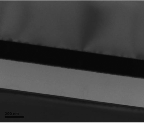
High resolution (HR) TEM (see Figure 3.19) images have been made on which no implantation residual defect is observed In this case the metal electrode is made of Pt, and the bonding layer (SiO2) is about 250 nm thick.
3.5. Design of experiments
The design of experiments is widely used in industry often through the use of software that manage the experiments being carried out and the exploitation of the results Software operation is often difficult to decipher This section aims to give some ideas about the use of this technique in the case of piezoelectric thin films.
Figure 3.19. HR TEM image of a stack of LiNbO3 transferred on a metal electrode (in this case Pt)
3.5.1. The assumptions
The semi-industrial environment of R&D centers often requires seasonal work on deposition machines, especially for exploratory work. This means that the development of a process should be as short as possible. To do this, it is possible to use a technique known as design of experiment (DOE). This method is based on the statistical treatment of experimental data. This does not mean that it is necessary to have a lot of experiments to address the problem. This is precisely about choosing carefully the experiments to be performed in order to minimize their number. Beyond the temporal interest in this technique, it requires thought to set up the experiment, which allows reviewing of several parameters that can usually be ignored. Another advantage of this technique is that it does not make the reproducibility assumption that is generally accepted during rapid experiments. Indeed, it actually checks reproducibility. The most severe assumption is that the out-of-control factors of the experiment have a very small effect on the measured value of the final parameter and the error that arises from the sum of their influences can be represented by a Gaussian function. This makes it possible to use the power of statistical computing, notably through the use of standard deviation.
In theory, DOE can model complex problems but, generally, the first screening phase is carried out assuming that each factor has a linear influence on the output parameter. Although restrictive, experience shows that this assumption is often sufficient to solve most of problems.
Let us give a simple example of DOE. Let us consider an experiment with three factors A, B, and C, each with two possible values: −1 or 1 (reduced values). If we wish to know the influence of these factors on a final parameter Y, we can realize the full factorial DOE described by the first eight experiments in Table 3.1.
Table 3.1. Full factorial design with three factors at two levels with three reproducibility experiments
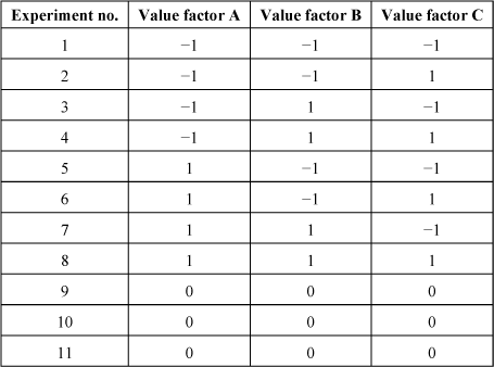
The organization is made so that orthogonality between the experiments is obtained. This means that if we choose the experiments with a particular value for a given parameter (for instance, value −1 for parameter A, corresponding to experiments 1–4), the other parameters take as many times the value −1 as +1 (as seen on the factors B and C).
If we make a linear assumption, the value of the output parameter can be described by the following equation:
[3.1] ![]()
The parameters aijk denote the linear coefficients whose value is obtained by the experiments. So we have eight experiments for eight coefficients to be determined.
Let us reconsider our previous example on the first four experiments in light of equation [3.1]. By summing the equations of these first four experiments, we obtain the following simple expression:
[3.2] ![]()
In fact, all terms other than A cancel out because of the orthogonality of the matrix. Thus, the resulting eight coefficients are easily obtained by summing the right combinations of the experiments results.
3.5.2. Reproducibility
The plan described above allows retrieval of all the influences of the first order between the three used factors. However, as the number of equations corresponds to the number of experiments, regardless of the quality of the experiments carried out, a solution will always be obtained, provided that the determinant of the matrix is not zero. This means that the model is not assessed. A solution for this is to undertake more experiments than necessary for the resolution of the system. Thus, some degrees of freedom are added to the system to check whether the model is consistent throughout the experimental domain or not. To illustrate this, we can keep only the terms without interaction between the factors in the previous example (see equation [3.1]), but keeping the eight experiments. The value of the output parameter is then described by the following equation:
[3.3] ![]()
Thus, the system has too many experiments for the number of coefficients to be determined. It is therefore necessary to introduce an experimental error. We use the assumption of a Gaussian error due to uncontrolled parameters of the experiments for this purpose.
The concept of reproducibility is introduced since it will be used to determine experimental standard deviation. Reproducibility can be performed in different ways. Statistics tell us that the ideal case would be to repeat each experimental point several times, but this is generally not possible. To limit the number of experiments needed, a new assumption is made that the experimental standard deviation is identical throughout the experimental domain. It is certainly not strictly valid but its magnitude is generally of the same order. This is often enough for a screening DOE. The determination of the experimental standard deviation is obtained, for example, through the realization of several experiments at the center of the experimental window, such as experiments 9, 10, and 11 in Table 3.1. The advantage of repeating the points that are not explicitly stated in the DOE is to verify the model at this point. Thus, the points at the center have a dual role: measuring the standard deviation of the Gaussian experimental error and assessing the model derived from the design. Indeed, it is noteworthy that the points at the center are not used to determine the model coefficients. The model extracted from experiments allows us to make predictions on the final parameter values based on the values of the factors. The formula derived from the statistical calculation giving the accuracy of the model is as follows (average formula) [BOX 78]:
[3.4] ![]()
sfusion is the estimate that we have of the standard deviation, n is the number of experiments that were conducted at the same point of the DOE or more generally the degrees of freedom and tstudent is the Student coefficient. The latter is a figure of merit of the knowledge we have on the standard deviation of the Gaussian. The more we have repeated experiments at the same point, the better we know our Gaussian, and the more the Student coefficient decreases. Its asymptotic value is 1.96 if we consider the case where the predictability of the model is set at 95% of confidence.
So, it is the number of degrees of freedom that is important to reduce this Student coefficient. To increase the number of degrees of freedom, it is possible to use the reproducibility experiments and, thus, calculate the standard deviation of the “remainders”. The remainders or residuals are defined as the difference between model and experiment at each point of the DOE. We should notice that a priori, nothing prevents us from saying that it is the same Gaussian that describes the experimental error and the error between model and experiment. Indeed, the statistical treatment guesses that the model is ideal. So the residual error is actually the experimental error.
There is a statistical test that indicates whether the experimental and residual standard deviations could come from the same Gaussian (Fisher test). If it is the case, we can thus merge the resulting standard deviations, which gives for the model a standard deviation merged with a number of degrees of freedom that corresponds to the sum of the degrees of freedom of experimental and residual standard deviations. It thus decreases the Student coefficient and the uncertainty on the model (see equation [3.4]).
3.5.3. How can we reduce the number of experiments?
The above example is a full factorial design, which means that we have crossed all the possible parameters to gather as much information as possible. It is possible to take a different approach and to reduce the number of experiments, which requires new assumptions. Thus, as a first step, the interactions between parameters can be neglected, which is not necessarily the case in reality. However, it is rare that an interaction between two parameters is strong when one parameter is low. A screening DOE is often carried out by neglecting higher order interactions. To illustrate the construction of such a design, here is an example of a fractional factorial design. Let us suppose that we add a fourth factor D in the previous experiment. This factor D is superimposed on the interaction of the three previous parameters ABC, which is supposed to be very low. The resulting design is given in Table 3.2. If the cross-interactions of more than two parameters are neglected, the linear equation that is solved with this design is the following:
[3.5] ![]()
Table 3.2. Fractional factorial design “one alias” with four factors at two levels and three reproducibility experiments
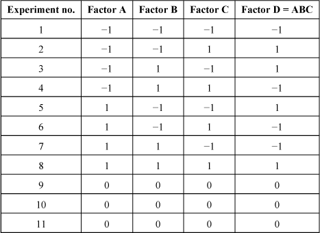
With the same number of experiments, it is possible to know the influence of four factors on the output parameter Y. The price to pay is that the interactions between more than two factors cannot be determined and that the interactions between two factors are coupled in pairs. In fact, these are the main effects that involve only one factor that can be calculated unambiguously. This reasoning can be developed even further by adding three new factors with the same number of experiments. To do this, the interactions between two factors of the full factorial design are superimposed on a new factor. The mixture between the interactions is then very strong but if all the interactions are neglected, the main effects of the seven parameters can be obtained with only eight experiments against 27=128 experiments for the full factorial design.
This example illustrates not only the power of the design of experiments but also their fragility. It is often possible to rationalize the number of experiments but we have to accept to perform “blind” experiments since the value taken by the various factors makes sense only through the whole DOE. This means that a DOE is only useful when it is entirely carried out; hence, a careful preliminary preparation of experimental conditions is very important. Finally, let us note that there are many different techniques using these DOE, sometimes with a very thorough theory [BOX 78].
As an example, we will detail in Section 3.5.4 a sputtering deposition optimization of PZT.
3.5.4. A DOE example: PZT RF magnetron sputtering deposition
This DOE was developed to optimize the deposition of PZT in terms of dielectric constant BF. The composition of PZT was measured through Rutherford Backscattering Spectroscopy (RBS). The samples that are used consist of a 100 mm substrate of Si oxidized over 500 nm followed by a TiO2 adhesion layer of 20 nm, then 100 nm of Pt sputtered at 300°C. The deposition technique of Pt is an RF magnetron sputtering (100 mm-Alcatel Puma 500 equipment). The target consists of PZT ceramic sintered in the morphotropic phase (Zr/Ti = 52/48) with a PbO excess of 10%, to compensate for the PbO loss experienced during the deposition and the final annealing. Four factors were surveyed in this design: the deposition pressure, the RF power, the sample temperature during deposition, and adding or not a thin layer of 5 nm TiO2 prior to the PZT deposition. The final crystallization annealing, mandatory to reach the desired perovskite phase for PZT, was performed in a conventional oven in air for 30 min after the deposition and the lift-off pattern of the Pt top electrodes in Pt. Several temperatures were tested on the whole set of samples: 550°C, 600°C, 650°C, and 700°C.
Table 3.3 details the DOE carried out. This is a fractional design with one alias, sometimes called 23−1.
Table 3.3. DOE made for the optimization of the dielectric constant of sputtered PZT
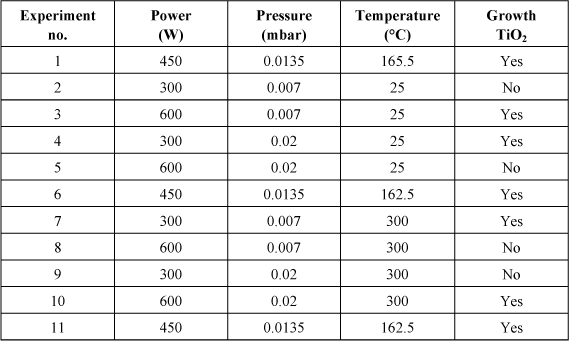
Each factor of the DOE takes two extreme values and the value at the center of the domain is used to measure reproducibility. The design includes eight specific experiments and three additional experiments of reproducibility that are performed at the beginning, middle and end to monitor any drift over time. Prior to the realization of this design, each experiment is tested to check the stability of the plasma and measure the deposition speed. In fact, since thickness plays an important role on the dielectric constant in perovskites through the interface effect, it is important to compare layers that have substantially the same thickness. Deposition time is therefore adjusted for each experiment to achieve thickness between 200 nm and 300 nm for each experiment.
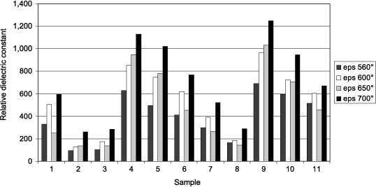
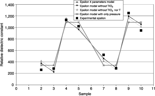
Figure 3.20 shows the relative dielectric constant εr measured on each sample (HP 4194A–10 kHz – 5 measurements per sample – Cp-D model at 0 V DC – 100 mV AC – top electrode diameter: 110 μm). Each experiment number and annealing temperature corresponds to a sample (44 samples in total). The largest dielectric constant reaches 1,240, which is consistent with the literature. The temperature at which εr is the highest is 700°C, which suggests a better crystallization of PZT in the perovskite phase. Although εr vary with the annealing temperature, their distribution is almost the same at a given temperature. The reproducibility samples (1, 6, and 11) do not provide exactly the same values but their uniformity sounds reasonably good. Moreover, it appears that these reproducibility samples are made of a phase mixture as discussed later. This transition zone between amorphous and crystalline phase disturbs capacity measurement.
Figure 3.20. Dielectric constant of the sputtered PZT extracted from measurements of C(0) at different deposition and annealing conditions
For the following, we focus on the samples annealed at 700°C. εr at 700°C are used to extract a model according to the methodology explained above. The reproducibility experiments (1, 6, and 11) are not used to calculate the model coefficients. However, they give the experimental standard deviation and are used to assess the model. Figure 3.21 compares the model and experiment of εr as a function of factors selected for the extraction of the model. A very strong dominance of the sputtering pressure can be noticed. This parameter alone is indeed sufficient to explain most of the variations in the dielectric constants. The higher the pressure, the higher is the dielectric constant.
By keeping only the pressure at the first order, the model is simplified to a linear equation with two unknowns. With eight experiments, the number of the degrees of freedom on the residual standard deviation reaches 6. Moreover, the experimental standard deviation derived from the reproducibility experiments is 85 with 2 degrees of freedom. Fisher's test allows us to merge the two standard deviations, which is then 117 with 8 degrees of freedom. The Student coefficient t8 at 95% confidence is 2.3. By applying the formula of the average to the three samples in the center of the experimental domain, the model predicts a εr between 556 and 867 at 95% confidence. Besides, the experimental εr of these three samples are 600, 670, and 770, which are indeed within the confidence interval. Therefore, this validates the pressure linear model extracted from the DOE to explain the behavior of εr of the sputtered PZT.
Figure 3.21. Model-experiment comparison of the dielectric constant of PZT sputtered as a function of the factors selected to extract the model. The points of reproducibility are not taken into account
The parameters' effect on the PZT composition was assessed through RBS and the results are shown in Figure 3.22. It should be noted that these samples were deposited on Si to improve RBS measurement. Indeed, a preliminary RBS simulation showed an overlapping of peaks in the analysis if Pt was present. The analyses are thus performed on non-annealed samples to prevent any diffusion of PZT into the Si.
Here again, sputtering pressure is sufficient to explain almost completely the Pb/(Zr + Ti) ratio. In fact, samples 4, 5, 9, and 10 have the highest Pb rate and it is those that have been deposited at higher pressure. Zr/Ti ratio is almost stable. However, a slight advantage for Zr should be noted when the pressure is high. This can affect the position of PZT on the phase diagram. As the nominal composition (Zr/Ti = 52/48) is the so-called morphotropic zone, this variation of Zr/Ti can lead to changes in electrical properties. Since these variations are correlated with that of Pb, it is impossible to isolate the role of each one. However, it is clear that the variation of the lead ratio is decisive because the dielectric constant changes are too important to be explained simply by a variation of the Zr/Ti ratio in the phase diagram of PbTiO3–PbZrO3.
Figure 3.22. Chemical composition of sputtered PZT as measured by RBS. PZT samples were deposited directly on Si to avoid any influence of Pt. No annealing was performed on these samples
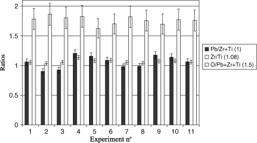
Oxygen is not well estimated through RBS (±10%) compared to the other elements (±5%). The experimental error plotted in Figure 3.22 suggests that the changes in oxygen are probably not significant. However, the average O/(Pb+Zr+Ti) ratio (1.76) is slightly higher than the ideal rate (1.5), which is indeed significant. The final rate of oxygen in the layer is adjusted during the final annealing, which is done under air. Let us remember that these composition measurements were made on non annealed samples. Finally, there is no correlation between the electrical properties and the oxygen rate measured before annealing.
The correlation between εr and lead ratio in the layer before annealing is shown by plotting εr as a function of the Pb/Zr + Ti ratio (see Figure 3.23). We obtain a straight line with a very good correlation factor (R2 = 0.94), which proves the link between permittivity and lead ratio in the layer. Theoretically, the Pb/Zr + Ti ratio should be close to 1 for the perovskite lattice. We observe that a ratio greater than 1 seems to increase εr according to Figure 3.23. It is likely that a part of Pb is removed during crystallization annealing because PbO is volatile. Moreover, an excess of Pb in the PZT is not necessarily bad for PZT as spotted by Hiboux [HIB 01]. He explained that the excess of Pb can be placed on the B site of the perovskite lattice with a behavior very close to Zr. It has been observed that this phenomenon explains the shift of the morphotropic phase in thin layers compared to bulk.
Figure 3.23. Relative dielectric constant as a function of the ratio Pb/Zr + Ti measured in RBS
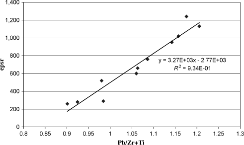
One possible explanation of the increase in Pb rate with pressure is the following. Increasing the sputtering pressure decreases the mean free path of the species in plasma. Therefore, the energy of the incident atoms on the sample decreases with pressure. In addition, since sputtering takes place at temperatures that are below crystallization (no phase observed by X-ray diffraction after deposition), the species that are present in the sample are most likely oxides of Pb, Zr, and Ti that are the most stable compounds. However, the PbO is the species that has the lowest surface energy. Thus, it is mostly found on the surface of the sample. Therefore, it is first re-sputtered by the incident species on the sample. If the energy of the incidents decreases, this re-sputtering decreases and the Pb amount is maintained in the sample.
3.6. Conclusion
This example illustrates how to conduct a study of materials optimization. The main advantage of DOE is completeness in the experimental domain. In addition, the analysis of the results is done through the basic use of statistical tools. The main drawback is the fragility of the design in the sense that all experiments should work to produce a final result, which is not always obvious. Often, this approach gives very good results to secure a process window.
3.7. Bibliography
[BER 84] BERTIN M., FAROUX J.P., RENAULT J., Cours de Thermodynamique, Dunod Paris, 1984.
[BIG 05] BIGOT C. et al., Solid State Phenomena, 180–109, 297, 2005.
[BOU 05] BOUYSSOU E., JERISIAN R., CEZAC N., LEDUC P., GUEGAN G., ANCEAU C., “Wafer level reliability and leakage current modeling of PZT capacitors”, Material Science and Engineering B, vol. 118, no. 28, 2005.
[BOX 78] BOX G.E.P., HUNTER W.G., HUNTER J.S., Statistics for Experimenters: An Introduction to Design, Data Analysis, and Model Building, John Wiley & Sons, New York, 1978.
[BRU 95] BRUEL M., “Silicon on insulator material technology”, Electronic Letters, vol. 31, no. 14, pp. 1201–1202, 1995.
[BUD 85] BUDD K.D., DEY S.K., PAYNE D.A., “Sol-gel processing of PT, PZ, PZT and PLZT thin films”, British Ceramic Proceedings, pp. 107–121, 1985.
[CAL 07] CALAME F., MURALT P., Applied Physics Letters, vol. 93, p. 62907, 2007.
[DAM 98] DAMJANOVIC D., “Ferroelectric, dielectric and piezoelectric properties of ferroelectric thin films and ceramics”, Reports on Progress in Physics, vol. 61, pp. 1267–1324, 1998.
[DEF 03] DEFAŸ E., ANDRE B., BAUME F., TARTAVEL G., MUYARD D., ULMER L., Ferroelectrics, vol. 288, pp. 121–132, 2003.
[DEG 05] DEGUET C. et al., 200 mm Germanium-On-Insulator (GeOI) Structures Realized from Epitaxial Germanium Wafers by the Smart Cut™ Technology, Electro Chemical Society, 2005.
[DEV 49] DEVONSHIRE A.F., Philosophical Magazine, vol. 40, p. 1040, 1949.
[DIC 97] DICIOCCIO L., LETERTRE F., LE TIEC Y., PAPON A.M., JAUSSIAUD C., BRUEL M., “Silicon carbide on insulator formation by Smart Cut™ process”, Master of Science and Engineering, vol. B46, pp. 349–356, 1997.
[FUJ 07] FUJII E., TAKAYAMA R., NOMURA K., MURATA A., HIRASAWA T., TOMOZAWA A., FUJII S., KAMADA T., TORII H., IEEE Transactions on Ultrasonics, Ferroelectrics and Frequency Control, vol. 54, pp. 2431–2438, 2007.
[GRO 52] GROVE W.R., Philosophical Transactions, vol. 142, no. 87, Roy. Soc., London, 1852.
[GUR 84] GURKOVICH S.R., BLUM J.B., Preparation of Monolithic Lead-titanate by Sol-gel Process, in Ultrastructure Processing of Ceramics, Glasses and Composites, L.L.Ha.D.R. Ulrich, Wiley-Interscience, New York, pp. 152–160, 1984.
[HIB 01] HIBOUX S., Thesis, Ecole polytechnique de Lausanne, 2001.
[HUH 09] HU H., RICKEN R., SOHLER W., “Large area, crystal bonded LiNbO3 thin films and ridge waveguides of high refractive index contrast”, Topical Meeting Photorefractive Materials, Effects and Devices, Control of Light and Matter, 2009.
[IEE 87] IEEE, Standard on Piezoelectricity, ANSI/IEEE Std 176, 1987.
[JAL 98] JALAGUIER E., ASPAR B., POCAS S., MICHAUD J.F., ZUSSY M., PAPON A.M., BRUEL M., “Transfer of thin GaAs film on silicon substrate by proton implantation process”, Electronic Letters, vol. 34, no. 4, pp. 408–409, 1998.
[JAL 99] JALAGUIER E., ASPAR B., POCAS S., MICHAUD J.F., PAPON A.M., BRUEL M., “Transfer of thin InP film onto silicon substrate by proton implantation process”, IEEE Proceedings of 11th International Conference on Indium Phosphide and Related Materials, Davos, 1999.
[JUN 03] JUNQUERA J., GHOSEZ P., “Critical thickness for ferroelectricity in perovskite ultrathin films”, Nature, vol. 422, pp. 506–509, 2003.
[LEV 98] LEVY M., OSGOOD R.M., LIU R., CROSS L.E., CARGILL G.S., KUMAR A., BAKHRU H., “Fabrication of single-crystal lithium niobate films by crystal ion slicing”, Applied Physics Letters, vol. 73, no. 16, p. 2293, 1998.
[LIN 77] LINES E.M., GLASS A.M., Principles and Applications of Ferroelectrics and Related Materials, Clarendon Press, Oxford, 1977.
[MAS 50] MASON W.P., Piezoelectric Crystals and Their Application to Ultrasonics, p. 289, D. Van Nostrand Company, Princeton, New Jersey, USA, 1950.
[MCC 91] MCCLANAHAN E.D., LAEGREID N., “Production of thin films by controlled deposition of sputtered material”, Sputtering by Particle Bombardment III, SpringerVerlag, Berlin, pp. 339–377, 1991.
[OSU 07] OSUGI Y., YOSHINO T., SUZUKI K., HIRAI T., “Single crystal FBAR with LiNbO3 and LiTaO3 piezoelectric substance layers”, Institute of Electrical and Electronics Engineers, pp. 873–876, 2007.
[PAR 06] PARK Y.B., MIN B., VAHALA J., ATWATER H.A., “Integration of single-crystal LiNbO3 thin film on silicon by laser irradiation and ion implantation-induced layer transfer”, Advanced Materials, vol. 18, p. 1533, 2006.
[PAS 07] PASTUREAUD T., SOLAL M., BIASSE B., ASPAR B., BRIOT J.B., DANIAU W., STEICHEN W., LARDAT R., VLAUDE I., LAËNS A., FRIEDT J.M., BALLANDRAS S., “High-frequency surface acoustic waves excited on thin-oriented LiNbO3 single-crystal layers transferred onto silicon”, IEEE Transactions on Ultrasonics and Frequency Control, pp. 54–4, 2007.
[RAD 03] RADU I., SZAFRANIAK I., SCHOLZ R., ALEXE M., GÖSELE U., “Ferroelectric oxide single-crystalline layers by wafer bonding and hydrogen/helium implantation”, Mat. Res. Soc. Symp. Proc., vol. 748, 2003.
[REI 65] REIF F., Statistical Physics, Berkeley Physics Course, vol. 5, McGraw-Hill, London, 1965.
[SAK 91] SAKASHITA Y., ONON T., SEGAWA H., TOMINAGA K., OKADA M., Journal of Applied Physics, vol. 69, pp. 8352–8357, 1991.
[SOU 06] SOUSBIE N., CAPELLO L., EYMERY J., RIEUTORD F., LAGAHE C., “X-ray scattering study of hydrogen implantation in silicon”, Journal of Applied Physics, vol. 99, art. 103509, 2006.
[TAU 05] TAUZIN A., AKATSU T., RABAROT M., DECHAMP J., “Transfers of 2-inch GaN films onto sapphire substrates using Smart Cut™ technology”, Electronics Letters, vol. 41, no. 1126, May 2005.
[VIL 03] VILQUIN B., Thesis, Caen, 2003.
[VRE 06] VREJOIU I., LE RHUN G., PINTILIE L., HESSE D., ALEXE M., GOESELE U., “Intrinsic ferroelectric properties of strained tetragonal PbZr0.2Ti0.8O3 obtained on layer-by-layer grown, defect-free single crystalline films”, Advanced Materials, vol. 18, pp. 1657–1661, 2006.
[VRE 07] VREJOIU I., ZHU Y.L., LE RHUN G., SCHUBERT M.A., HESSE D., ALEXE M., “Structure and properties of epitaxial ferroelectric PbZr0.4Ti0.6O3/PbZr0.6Ti0.4O3 superlattices grown on SrTiO3(001) by pulsed laser deposition”, Applied Physics Letters, vol. 90, 072909, 2007.
[WAN 01] QING W., LIANWEI W., WEILI L., MIAO Z., CHENGLU L., “Investigation of H+ and B+/H+ implantation in LiTaO3 single crystals. Nuclear instruments and methods”, Physics Research, vol. B184, p. 531, 2001.
[WUC 06] WU C.C., HORNG R.H., WUU D.S., CHEN T.N., HO S.S., TING C.J., TSAI H.Y., “Thinning technology for lithium niobate wafer by surface activated bonding and chemical mechanical polishing”, Journal of Applied Physics, vol. 45–4B, pp. 3822–3827, 2006.
[YAM 91] YAMAMOTO K., MIZUUCHI K., TAKESHIGE K., SASAI Y., TANIUCHI T., “Characteristics of periodically domain-inverted LiNbO3 and LiTaO3 waveguides for second harmonic generation”, Applied Physics Letters, vol. 70, no. 4, 1991.
[ZHU 10] ZHU X.H., DEFAŸ E., GUIGUES B., LE RHUN G., DUBARRY C., AÏD M., Journal of European Ceramic Society, vol. 30, pp. 471–474, 2010.
1 Chapter written by Chrystel DEGUET, Gwenaël LE RHUN, Bertrand VILQUIN and Emmanuel DEFAŸ.