
14
Multimode Multiband Terminal Design Challenges
Jean-Marc Lemenager, Luigi Di Capua, Victor Wilkerson, Mikaël Guenais, Thierry Meslet, and Laurent Noël
The mobile phone industry has experienced unprecedented growth since it was first launched over 20 years ago using 2G/ EDGE, GSM, GPRS (EGPRS) technologies. Combined with 3G standards, such as WCDMA/HSPA, and more recently, 4G/LTE (FDD and TDD), mobile phone shipments have continuously beaten records, tripling volumes from 533 million devices in 2003 to more than 1.8 billion devices in 2013. Looking ahead to 2017, it is expected that shipments of mobile phones will then reach 2.1 billion units worldwide [1]. Put into perspective, this means that nearly 70 devices will be shipped every second! Beyond these impressive production volumes, the introduction of smartphones in 2007, unleashed by Apple's original iPhone, is the other major factor that has completely reshaped the definition of mobile terminals. A high-end non touch-screen 2009 device would today be qualified as “feature phone” or “voice-centric phone.” The year 2013 was a key turning point in the history of this industry as the “data-centric / do-it-all” smartphone shipments exceeded the volumes for these feature phones. Based on current trends, what are now collectively called “smartphones” are likely to transition to a market segmented into three retail price ranges: low end/cost (<100$), mid-end (<300$), and high-end super-phones (>500$). Given this expectation, it will become difficult to make a distinction between these segments, based on a common classification as “smartphones.” This is not unlike the trend seen in the world of PCs. In the high-end segment, the differentiator is likely to translate into a race to be the first to deliver new hardware (HW) or telecom features, such as being the first device to support LTE-Advanced. In the lower-end segment, retail prices will be the primary differentiator.
The other key factor which has influenced the situation is the quick pace at which 3GPP has been delivering new telecom features and air-interfaces, moving from the well established mono-mode EGPRS terminal, then to dual-mode EGPRS-WCDMA, and more recently to the triple-mode EGPRS/WCDMA/LTE user equipment (UE). Some of the most recent smartphones also have to support a fourth air interface: TD-LTE. Commensurate with support for this evolution comes the necessity to support more frequency bands. The rate at which bands have been introduced by 3GPP is illustrated in Figure 14.1, which plots the number of bands vs. the initial introductory years for LTE-FDD (36.101) and WCDMA/HSPA (25.101). With the introduction of LTE, the number of bands standardized at 3GPP as of October 2013 is 29 FDD bands and 12 TDD bands (TDD bands are not shown in Figure 14.1). This trend is not expected to abate as the UARFCN formulae are modified to accommodate up to 128 bands in future releases [2]. The table inserted in Figure 14.1 shows that the number of bands supported in mobile phones has followed a similar trend. From 2003 to 2006–2007, dual-mode terminals only needed to support a small number of bands: band I for most networks, plus band II and V in North America. Today, worldwide roaming is achieved in dual-mode terminals by supporting a total of nine bands: four EGPRS (850,900,1800,1900) and five WCDMA bands (I, II, IV, V, VIII).
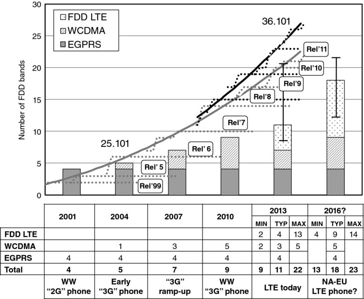
Figure 14.1 Number of frequency bands for WCDMA (TS25.101 -UTRA) and LTE (TS36.101 – E-UTRA) air interfaces vs. typical commercial UE band support per air interface (bar graph)
Figure 14.2 is a depiction of the most common bands deployed worldwide, and helps to better illustrate the complexity of multiple band support for multimode terminals. The map is complemented with a short table listing the band support requirements for three hypothetical geographical regions: worldwide (WW), North America – Europe combined (NA-EU), and EU only triple-mode terminals. Global WW dual-mode requirements are provided as a baseline for comparison purposes. These examples highlight the impact of adding LTE support: while 9 bands is all that is required to cover the world in a dual-mode terminal, the triple-mode UE needs to support 24 bands (20 FDD, 4 EGPRS); and this becomes 27 if TD-LTE is to be supported. With 9 bands, the triple-mode terminal can only cover the EU market. Remarkably, the number of bands required to provide just NA-EU coverage in a triple mode terminal1 is double that of a dual-mode WW phone: 18 bands vs. 9 bands for dual-mode handset. Of course, this situation is somewhat offset by the fact that doubling the number of bands does not necessarily translate into doubling the number of power amplifiers and/or RF filters, thanks to the concept of co-banding2. However, even with co-banding, the explosion in the number of bands supported imposes some new constraints. Today, the triple-mode WW “flagship” terminal must be realized using several variants, each covering a particular region of the world/ecosystem. Even dual-mode terminals are frequently produced using several variants to deliver the best roaming/cost compromise. However, the need to support a large number of bands is not, in itself, the most critical problem. Not long ago, the same situation existed for the dual-mode phone, where supporting five WCDMA bands seemed difficult to achieve at minimal cost increase. Rather, the primary challenge introduced by the existing ecosystems is that each have telecom operator-specific and/or region specific band combinations which do not overlap. This in turn translates into having to develop several variants of a mobile phone. The problem is not expected to improve in the longer term as carrier aggregation introduces additional operator specific frequency band combinations.
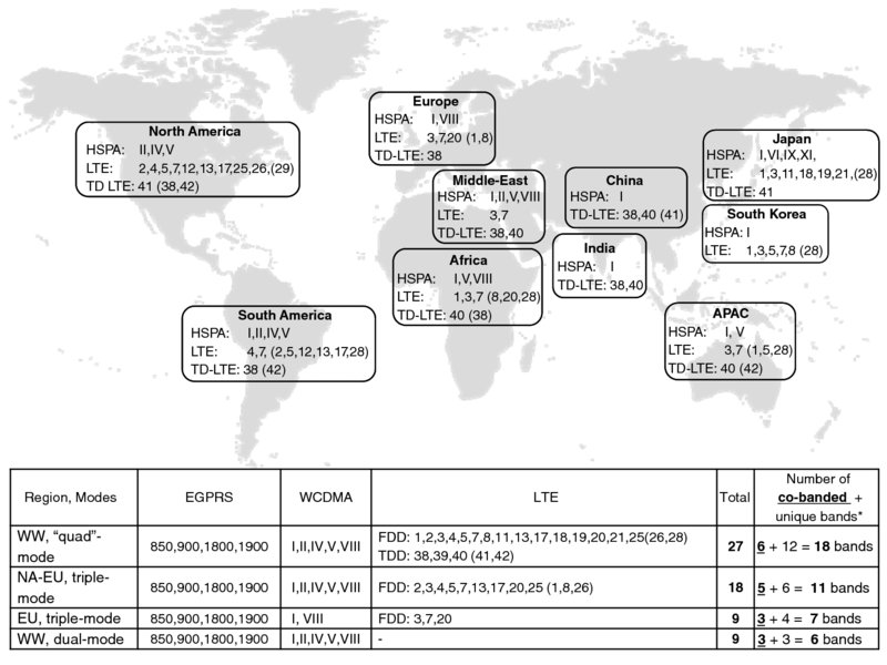
Figure 14.2 Main commercial frequency bands and band requirements for multimode terminals. Future LTE commercial bands are shown in brackets. The number bands that can be shared amongst RAT or “co-banded” are underlined
In this competitive and changing environment, the dynamics of the mobile phone industry translates into seemingly conflicting cost/feature/performance requirements – can the next generation platform deliver more hardware features (e.g., more bands, modes, peripherals, etc.) at the same cost, or even at a lower cost, than the previous generation, and yet offer an improvement in performance? This chapter aims to illustrate the innovations of the past 10 years, and to use these as a basis to describe the future opportunities to address these ever-increasing challenges. A discussion on the tradeoffs between cost and performance resulting from these requirements is presented using two metrics: those of component count and PCB footprint area for cost constraints, and power consumption for performance needs. This chapter invites readers to take a journey to the center of a multimode multiband terminal through the selected subsystems of Figure 14.3. Each subsection provides a focused view of that particular area or function. Section 14.1 covers design tradeoffs within the constraints of cost reduction. Section 14.2 presents techniques and challenges experienced in delivering the optimum power consumption with a focus on two key contributors: the application engine and the cellular power amplifier. Many other key aspects encountered in modern terminal designs deserve attention, but cannot be covered within the scope of this short overview.
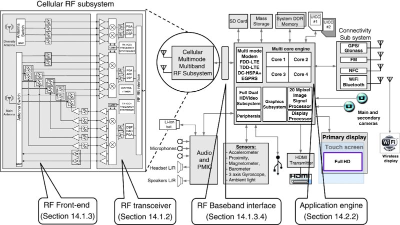
Figure 14.3 Generic multimode multiband terminal top level block diagram
This chapter aims to show that, in this highly competitive and complex ecosystem, the key to winning designs is to deliver easily reconfigurable, highly integrated hardware solutions. In this respect, LTE is included in most subsections, since it becomes less and less cost-effective to deliver dual-mode-only chipsets.
14.1 Cost Reduction in Multimode Multiband Terminals
14.1.1 Evolution of Silicon Area and Component Count
The trend in mobile phone hardware cost metrics is illustrated in Figure 14.4, by plotting component footprint area and total component count vs. year of introduction. The graph is generated with data extracted from the teardown reports of 69 mono-mode, 48 dual-mode, and 7 triple-mode handsets [3]. While the total number of components in EGPRS has remained virtually constant from 1996 to 2005, the required area has been reduced considerably over that time – from 14 cm2 (1998) to reach a minimum at approximately 5 cm2 (2006–present). This represents a reduction of about 65%. The maturity plateau has been reached thanks to highly integrated single chip solutions in which four key components are integrated into a single die: RF transceiver, baseband modem, power management unit, and multimedia processor. It took dual-mode handsets only four to five years to reach the level of complexity that took nearly eight years to reach in the GSM realm. Due to the low number of teardown reports available at the time of printing, it is difficult to make an accurate assessment of the trend in triple-mode devices. The metrics tend to show that the introduction of LTE has not significantly increased the cost of a dual-mode smartphone. The step occurring around 2009–2010 is primarily due to the shift in complexity between the voice centric “feature” phones and feature rich smartphones. The trend shows that these remarkable achievements were accomplished by higher levels of component integration and miniaturization. These improvements must also be offset against the simultaneous increase in mobile phone features. In 1998, handsets used monochrome LCD screens and lacked any significant multimedia capabilities. This is in stark contrast to the latest “super-phone” devices, some supporting full HD screens, which will soon be able to decode 4 K video resolution, a feature that is barely supported by cable TV decoders. Section 14.1.2 zooms in on the RF subsystem and shows how fast the 2013 LTE solutions managed to reach the same level of complexity as the most optimized dual-mode platforms.
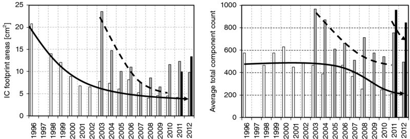
Figure 14.4 Mobile phone stacked IC footprint area3 and total component count vs. year vs. supported modes. White: mono-mode EGPRS feature phones, Gray: dual-mode EGPRS-WCDMA (2003–2009 “feature” phones, 2010–2012 “smartphones”), Black: triple-mode EGPRS, WCDMA, LTE “smartphones”
14.1.2 Transceiver Architecture Evolutions
WCDMA has been in production for a little more than 10 years. But, over this decade, the RF subsystem has undergone tremendous changes. Through the selection of various RF transceiver architectures, as presented in Figure 14.5, this section aims to illustrate the efforts made by the industry to reduce costs, while also answering the demand for more modes and more bands. What a change between the early mono band I WCDMA UE (solution (a, b, c) Figure 14.5) and the recent triple mode LTE-HSPA-EGPRS phone. In this section will be shown the evolution of design challenges, which enabled reducing PCB area by a factor 4, and component count by 1.6, all while supporting nearly 3 times more frequency bands and one extra mode: LTE.

Figure 14.5 10 years of RF subsystem PCB evolutions4. PCB pictures relative scaling is adjusted to illustrate relative size comparison (a) WCDMA super-heterodyne RX IC, (b) WCDMA super heterodyne TX IC, (c) EGPRS transceiver IC, (d) WCDMA DCA transceiver, (e) EGPRS transceiver, (f) Single-chip dual-mode EGPRS and WCDMA transceiver, (g) Single-chip dual-mode with RX diversity EGPRS and WCDMA transceiver, (h and i) single-chip triple-mode with RX diversity EGPRS, WCMDA, LTE FDD (and GPS RX)
In the early years of deployment, WCDMA received criticism for lack of devices and poor battery life. Under this pressure, the challenge for first-generation transceiver (TRX) designs consisted of delivering low risk, yet quick time-to-market, solutions, sometimes at the expense of cost (high BOM) and power consumption. The choice of architecture was frequently influenced by the two- to three-year-long development cycle required for a cellular chip set. And, once a platform is released, OEMs need at least an extra five to eight months to get a UE ready for mass production. To minimize risk, some of these early generations selected the super-heterodyne architecture, requiring three RF ICs (Figure 14.5a, b, c): one WCDMA receiver and transmitter IC, and a companion EGPRS transceiver (TRX). With two Intermediate Frequency (IF) Surface Acoustic Wave (SAW) filters and two RF filters required per chain and per band, an associated complex local oscillator (LO) frequency plan, a high power consumption, and an intrinsically-high component count, super-heterodynes were not suited to meet the longer-term multiband and multimode requirements of modern handsets. The resulting priority, then, was to focus R&D efforts on reducing component count by delivering single chip TRX solutions.
Direct Conversion Architecture (DCA) is an ideal solution to achieve this goal because the received carrier is converted, in a single RF mixing conversion process, to baseband in-phase/quadrature (IQ) signals. The same principle, in reverse, applies to the transmit chain, a concept sometimes referred to as Zero-IF. For a long time, the DCA was not put into production due to problems with DC-offsets/self-mixing, sensitivity to IQ mismatches, and flicker noise. The use of fully-differential architectures, along with adequate manufacturing processes and design models, made IC production using these principles a reality in around 1995 for EGPRS terminals. Numerous advantages make this technology essential in dual-mode handsets: substantial cost and PCB footprint area is saved by removing the heterodyne IF filters. An example of this is presented in Figure 14.5d and e, where early WCDMA single-chip DCA solutions (2006–2007) reduce PCB area by a factor 4, and used 2.5 times fewer components than the super-heterodyne (Figure 14.5a, b, c) solution. Moreover, with its single PLL, the DCA not only contributes to reducing power consumption, but also provides a flexible solution to the design of multiple band RF subsystems. Additionally, this architectural approach is future-proof, since multimode operation consists in simply reconfiguring the cut-off frequency of the I/Q low pass channel filters.
As WCDMA technology started gaining commercial momentum, staying in the lead meant racing to deliver solutions that supported multiple WCDMA bands. Despite its numerous advantages, multiband support was not cost-efficient for early DCA commercial implementations because it required two external inter-stage RF SAW filters per band: one filter between the LNA and mixer in receive, and another between the TX modulator output and the power amplifier (PA) input in transmit.
In the receiver chain, filtering is required to reject the transmitter carrier leakage when the UE is operated near its maximum output power. In this case, it is not unusual for PAs to operate at 26-27 dBm output power to compensate for front-end insertion losses. The requirement to support more bands, and in the case of LTE the need to support more complex carrier aggregation scenarios, results in increasing RF front-end insertion losses. This, in turn, means that the PA maximum output power requirements may exceed 27 dBm in certain platforms. Because duplexer isolation is finite, TX carrier leakage can reach the LNA input port with a power as high as −25 dBm. In the presence of this “jammer,” the mixer generates enough baseband products through second order distortion5 to degrade sensitivity, thereby partially contributing to a phenomenon known as UE self-desensitization, or “desense” [4]. In this case, and depending on system dimensioning assumptions, RX SAW-less operation sets a stringent mixer IIP2 requirement on the order of 48 to 53 dBm (LNA input-referred) [4].
In the transmitter chain, further UE self-desense occurs due to TRX and PA noise emissions generated at the duplex distance. Depending on duplexer isolation, SAW-less operation sets TX noise requirements in the range of −160 dBc [4]. Meeting this requirement in bands with short duplex distances, such as band 13 or 17, constitutes a serious challenge to both TRX and duplexer designers as performance may become dominated by PA ACLR emissions rather than the far out of band noise level. The duplexer high-Q factor often pushes designers to trade isolation against insertion loss. In these bands, 3GPP has introduced relaxations to ease factors related to these design constraints [5].
As the number of bands to be supported was increasing rapidly, the race towards continuous cost reduction called for novel TRX architectures that would enable both TX and RX SAW-less operation. For example, removing the interstage filters in a penta-band RF subsystem may save the cost of a PA and the area of almost an entire RF transceiver6. SAW-less operation also means that RF transmitter ports can be shared between several RF bands. For example, a single low-band TX port could be used to support all UHF bands, for example, LTE bands 8, 13, 17, and 20. Similarly, a high band port could be shared to support either WCDMA or LTE transmissions in bands 1, 2, 3, 4. The SAW-less TX architecture is therefore the sine qua non to enable replacing discrete single-band PAs with a single multiband, multimode (MMMB) PA. The cost savings and design tradeoffs associated with the use of MMMB PAs are presented in Section 14.1.3.2 using a North American variant. Initial RX SAW-less commercial solutions appeared around 2008 (Figure 14.5f). Some of the techniques developed to meet the high IIP2 requirements range from careful design of fully differential structures, use of passive mixers or trap filters to reject TX leakage, as well as the integration of IIP2 calibration circuitry.
In contrast, TX SAW-less operation is more challenging and took a longer time to emerge since every block of the transmitter chain impacts the overall performance. The efforts required to meet the stringent −160 dBc requirement are illustrated in Figure 14.6a. This graph plots UE self-desense in a SAW-less application using the reported band I TRX noise performance7. With a desense less than a decibel under typical duplexer isolation, TX SAW removal started to become a reality around 2007–2008, and the first handsets using this technique made their appearance a couple of years later (Figure 14.5g). Note that bands with low duplex gap and distance, such as bands 13,17, may still require inter-stage filtering for certain vendors (Figure 14.5i). The primary principle for achieving low noise consists in minimizing the number of cascaded gain stages at RF. One example [6] proposes to carefully balance the 74 dB gain control range between digital, analog IQ, and a bank of parallel RF mixers. In [7] a single pre-amplifier RF stage made up of multiple parallel amplifiers delivers the equivalent of an RF power DAC. Each solution provides a mixture of pros and cons. For example, controlling carrier leakage in an architecture based on a bank of mixers can be a challenge at minimum output power, due to mixer mismatches. The mixers must deliver approximately −65 dBm8 output power with 15 to 20 dB LO rejection, so keeping LO leakage below −85 dBm while transmitting around 0 dBm sets, a non-trivial requirement on the LO-to-RF port isolation when dealing with multiple mixers. One key problem is not only to be able to implement an architecture which meets low noise requirements at high transmit powers, but also able to meet the high WCDMA dynamic range requirements with better than 0.5 dB gain step accuracy. The step size accuracy challenge can partially be solved using a high dynamic range IQ DAC. But for many years, these were either not available, or they consumed too much power.
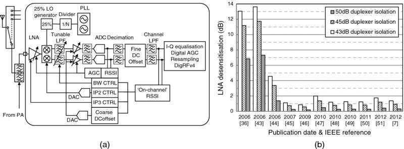
Figure 14.6 (a): Modern RF CMOS DCA receiver. Adapted from Xie et al. [8], (b): Evolution of LNA desensitization due to TX noise in a hypothetical TX SAW less application (IEEE survey). LNA input referred noise figure of transceiver is assumed to be 3 dB
Despite achieving an impressive level of integration, the BiCMOS solution in (Figure 14.5f) did not support RX diversity, a feature which was not absolutely necessary for early Cat-6 HSDPA terminals, but which quickly became mandatory for LTE operation. A series of factors pushed this technology from the forefront, in favor of CMOS. With digital BB production volumes moving rapidly from 130 nm to 28 nm, the lower cost of manufacturing made this technology process very attractive. Beyond the intrinsic cost advantage, using CMOS for the RF-IC implementation enabled novel architectures to deliver an unprecedented level of performance and power consumption. With low operating supply voltages, CMOS significantly lowers the power consumption of functions that were implemented in an analog fashion in BiCMOS designs. High dynamic range (HDR) ADCs [5] and DACs are key blocks which allow for a reduction in complexity for the analog low pass filters. For example, due to limited ADC resolution, the receiver in Figure 14.5f introduced rather complex auto-calibrated analog I/Q group delay equalizers to flatten the channel filter group delay distortions [9]. With high dynamic range ADCs, the role of the analog filter can be changed from a channel filtering to a simple anti-aliasing function. Not only is the filter complexity reduced as the filter order is relaxed, but also EVM performance is improved since the level of in-band distortion is kept to a minimum. Moreover, with most of the channel filtering implemented in digital filters, the difficulties in supporting multimode operation are eased, since reconfigurability then becomes a matter of reprogramming an FIR or an IIR filter. The emergence of a standardized digital baseband interface such as DigRFSMv4 (Section 14.1.3.4) has further facilitated the transition towards a more digital-oriented CMOS transceiver design. With microcontrollers now available at lower cost impact, traditional digital BB functions can be moved into the RF transceiver. An illustration of a modern DCA receiver is shown in Figure 14.6a, where the use of a Digital Signal Processor (DSP) allows automatic calibration of LNA IIP3 and IIP2 mixer, digital DC offset compensation, and I/Q image rejection correction to deliver a level of performance that would have been nearly impossible to achieve in analog BiCMOS designs. Comparing receiver [8] with solution (f) in Figure 14.5, 70 dBm IIP2 (vs. 58 dBm) provides ample margin for SAW-less operation and, with an EVM performance below 3% (vs. 6%), near zero impact on LTE/HSPA+ demodulation performance is expected. And all of this is also achieved at half the power consumption (43 mW vs. 92 mW). In Figure 14.5, transceivers (g), (h), and (i) are all designed in CMOS technology. Finally, designing in CMOS paves the way for a low-cost, highly integrated single-chip solution in which the RF TRX, the digital BB, and power management ICs may be manufactured in a single die. Initially developed for EGPRS low-cost terminals, monolithic solutions are now in production for HSPA and have recently been announced for triple-mode LTE platforms [10,11]. With such a high level of integration, only a handful of ICs is required to build the platform.
With the removal-of-SAW-filters challenge solved for the majority of commercial chip sets and frequency bands, what are the new challenges the industry faces today?
In single chip devices (also sometimes denoted as System-On-Chip, or “SoC”), the collocation of multiple noisy circuits next to the sensitive RF TX/RX chains create numerous co-existence challenges. Solving these myriad of co-existence issues is a fertile field of innovations, and is briefly introduced in Section 14.1.3.5.
Another interesting challenge lies in TRX IC area reduction. With the large number of bands required for a WW LTE solution, the number of LNAs to be integrated increases. The problem is exacerbated due to requirements for RX diversity for each band of operation. The resulting increase in number of RF ports is shown in Figure 14.7b. For example, a NA-EU triple mode LTE, HSPA+, EGPRS variant may require up to 32 RF ports9. This is a 50% increase compared to a typical dual-mode WW phone. Unfortunately, RF blocks, such as LNAs and RF PGAs, do not typically shrink with decreasing CMOS nodes. As Figure 14.5 shows, the area occupied by TRX packages has shrunk over the years, reaching, in early 2013, the ultimate Wafer Level Packages (WLP), in which the package is basically the size of the active die (25 mm2). If pin count continues to grow, the modern RF CMOS transceiver package size may be dominated by pin count. In solutions using differential LNAs, the RF ports of the NA_EU variant would require a total of 54 RF pins. With such a high number of ports, ensuring acceptable pin-to-pin isolation is also further complicated. Lastly, PCB routing becomes more complex because high pin density packages often require additional PCB layers, which further raises the total cost to manufacture.
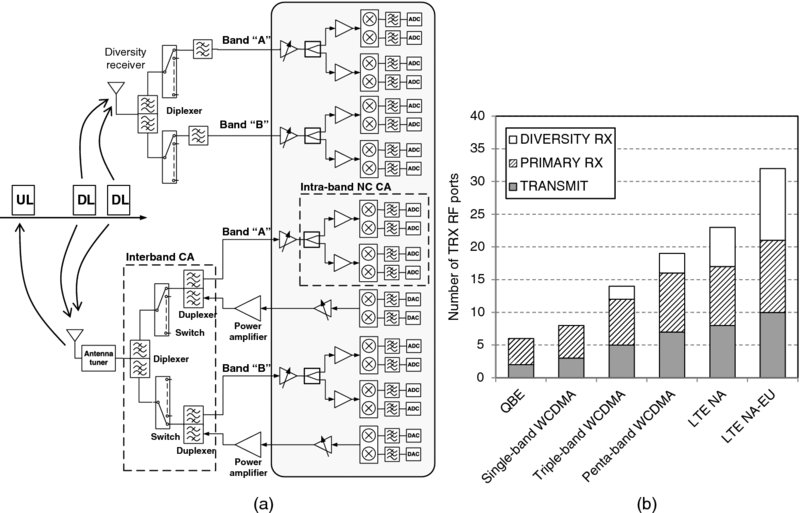
Figure 14.7 (a): Example RF front end complexity in supporting triple-mode and multiple downlink only carrier aggregation scenarios: contiguous and non-contiguous, intra and inter band. Only a pair of bands is shown. (b): RF transceiver number of RF ports required per application
Finally, the introduction of Carrier Aggregation (CA) adds complexity to the entire RF subsystem as illustrated in Figure 14.7a. There are three categories of CA scenarios from 3GPP: inter-band, intra-band contiguous (IB-C-CA), and intra-band non-contiguous (IB-NC-CA). The immediate impact on TRX design is the need to support greater modulation bandwidth. The initial commercial deployments started in August 2013 with 10+10 MHz. The next phase, 20+20, will start during 2014, thereby requesting UE receivers to support a total of 40 MHz BW. There are numerous interesting challenges associated with CA, but a detailed description would go far beyond the scope of this introduction. While most challenges impact the RF-FE linearity, filter rejection, and topology, the special case IB-NC-CA is problematic for the design of a single-chip TRX solution. In this CA category, the wanted downlink carriers may be located at, or near, the edges of a given band as depicted in Figure 14.8. This situation creates at least two types of new challenges.
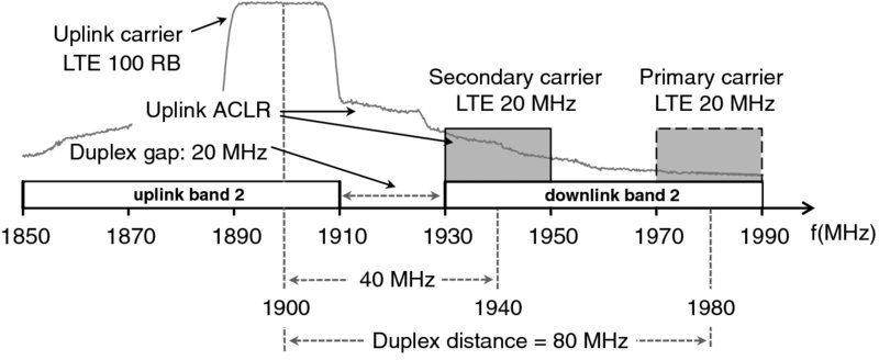
Figure 14.8 Example of worst case uplink–downlink carrier frequency spacing in the case of band 2 intra-band CA
The first problem results from the fact that, while the primary carrier is located at the duplex distance, the secondary carrier could be located at a distance slightly greater than the duplex gap (‘DG’ – cf. Figure 14.8). In bands with large DG, such as band 4, this is not an issue. But, for example, in the case of band 2, where the DG is only 20 MHz, the secondary carrier can be desensitized by the PA ACLR emissions. Thus even if inter-stage saw-filtering is applied, for certain combinations of uplink and downlink resource block allocations, the secondary downlink carrier sensitivity performance is degraded. This case is similar in nature to the desensitization occurring in band 13/17, where only a 3GPP performance relaxation can solve the issue. At the time of writing, these relaxations are being debated.
Secondly, it becomes apparent that opting for a single LNA/mixer chain to demodulate two carriers that could be located at the opposite edges of the band does not appear feasible for linearity and bandwidth reasons. As a consequence, a dual receiver and dual LO architecture is required to down-convert each carrier, as shown in Figure 14.7a. Contribution [12] summarizes in great detail the implications, and shows that due to limited isolation in a single-chip solution, cross-LO leakage occurs. In practice, this means that each mixer will not only be driven by its intended LO, but also by the leakage of the second LO, and by the multiple IMD products generated by non-linear mixing of the two LOs. The analysis indicates that requirements on cross-LO leakage and LO IMD product rejection might be difficult to achieve in a single chip. VCO-pulling is another phenomenon which is difficult to solve in single-chip devices. Pulling occurs when VCOs, operating either at close, or at harmonic, frequencies of another VCO, couple to one another, which may push the PLL to go out-of-lock. In the case of IB-NC-CA, [13] since carrier frequencies are signaled by the network, the reprogramming of VCO divide ratios has to be done “on the fly.” During this time, PLL synthesizers must be disabled and consequently IQ samples are interrupted. Only a 3GPP relaxation can help solve this issue. It is suggested to introduce a 2-ms interruption, a penalty equivalent to 4 LTE time-slots. Note that this issue is also applicable to inter-band CA. Finally, the problem is not expected to abate as the recent introduction of triple-band downlink carrier aggregation requires the UE to activate simultaneously four local oscillators (LO): one uplink and one for each downlink carrier, that is, 3 LOs in RX. Most triple-band combinations call for inter-band-CA, such as CA 4+17+30 or 2+4+13. But one special requirement combines all of the above mentioned challenges: CA 2+2+13 requires the UE to perform IB-NC-CA in band 2, plus inter-band CA with a carrier located in band 13.
14.1.3 RF Front End
The RF-FE includes a rich diversity of components ranging from RF filters, duplexers, diplexers, antenna switches, power amplifiers (PA), and other circuitry such as antenna tuners, sensors, directional couplers, and obviously antennae. In the RF TRX, multimode multiband operation is made possible via the use of reconfigurable architectures, mostly in the IQ domain and in the PLL/VCO blocks. Reconfigurability in the front-end is much more problematic, since it is difficult to implement tuneable RF filters without incurring either insertion loss or attenuation penalties. This section aims to illustrate the solutions found by the industry to address cost reduction in the front-end, while also meeting the needs posed by greater complexity.
14.1.3.1 Trends in Filters and Switches
In the receiver path, filters are used to eliminate the unwanted RF signals. In the transmit direction, they attenuate out-of-band noise and spurious emissions to ease coexistence effects between bands and terminals. For each supported FDD band of operation, Figure 14.10 shows that three filters and an antenna switch are required: two band-pass filters (BPF) in the duplexer and one BPF in the diversity receiver branch. The number of throws in antenna switches is driven by the number of bands that must be supported. For example, Figure 14.5 shows that switches have evolved from single pole 6 throw (SP6T) devices in 2003, to SP12T in 2013. This number is obviously bound to grow in coming years with increasing band count, support for LTE-TDD and Carrier Aggregation. Carrier Aggregation also raises additional RF performance requirements – improved linearity for example (Section 14.1.3.5) – and the need for a diplexer to further separate the aggregated bands.
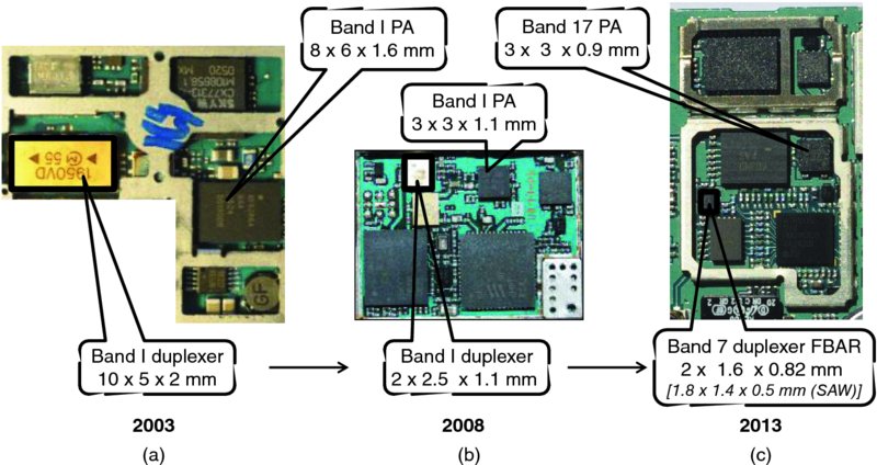
Figure 14.9 Example of duplexer miniaturization. (a): Ceramic 2003, (b): SAW 2008, (c): FBAR 2013 – PCB pictures are extracted from Figure 14.5 and scaled to reflect exact relative sizes
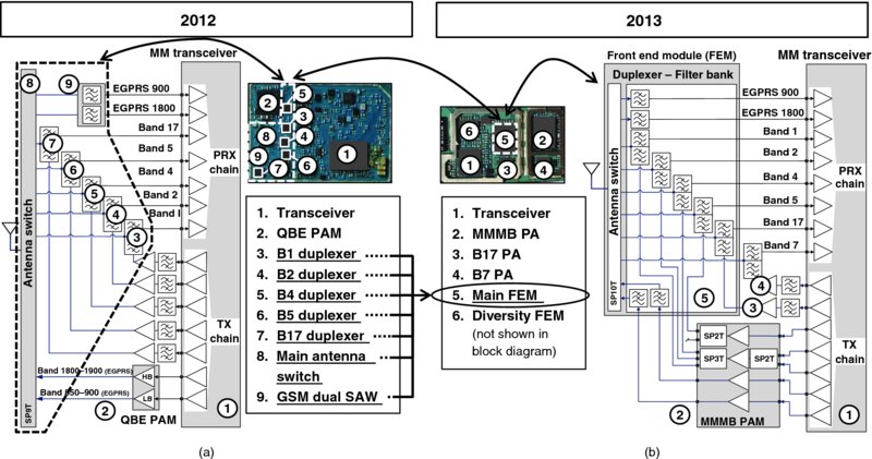
Figure 14.10 Enlargement of the RF front end of (block diagram11 and PCB pictures) of 2012 and 2013 terminals from Figure 14.5. (a): Discrete solution, (b): Integrated front end module example which supports quad-band EGPRS, WCDMA bands I, II, IV, V, and LTE bands 1, 2, 4, 5, 7, 17
For switches, only an improvement in technology can lead to significant cost reductions. Legacy GaAs PHEMT solutions are being replaced with cheaper single die SOI (Silicon on Insulator) semiconductor technology. In the world of RF filtering, the ideal solution would make use of tuneable RF filters to address cost reduction. Research is ongoing in this area and initial tuneable duplexers [14] show promising results, but these are far from meeting the stringent FDD operation isolation/insertion loss requirements. In practice, the approaches taken to reduce cost/PCB footprint area essentially fall into three categories: component miniaturization, co-banding, and module integration.
The main challenge in filter miniaturization has been and still remains to maintain low insertion loss while delivering high attenuation. Filter technology rapidly evolved from ceramic to SAW filters, a technology based on ceramic piezoelectric materials. It is complemented by silicon BAW/FBAR10 technology for the most demanding requirements related to short duplex distance and for frequency of operation beyond 2 GHz. An illustration of the efforts made for duplexers is shown in Figure 14.9: the size of the 2003 ceramic duplexer was 10 × 5 × 2 mm. SAW-based duplexers introduced around 2005–2008 shrank to 2 × 2.5 × 1.1 mm (Figure 14.9b), whereas the latest mass-produced models come in packages of 1.8 × 1.4 × 0.5 mm for SAW and 2.0 × 1.6 × 0.9 mm for FBAR (Figure 14.9c). Compared to the initial ceramic devices, the size is remarkably reduced to 1/15 in area ratio and 1/60 in volume ratio for SAW devices.
Co-banding is a technique which consists of sharing RF filters in bands for which multimode operation must be supported. For example, in band II (PCS 1900), rather than implementing an EGPRS RX chain with a dedicated PCS RX BPF, it is tempting to reuse the antenna to RX path of the band II/band 2 FDD duplexer required for LTE and HSPA operation. By routing EGPRS through the duplexer, one RF BPF is saved. The drawback of this approach is that the duplexer insertion losses are usually higher than that of a standalone BPF, thereby leading to a slight degradation in EGPRS sensitivity. An example of co-banding is shown in Figure 14.5g (2011). In practical terms, if co-banding was applied to UE [15], the 17 frequency bands supported by this terminal could be reduced to only 8 unique RF receiver paths and 4 transmitter line-ups: bands 1, 2, 5, and 8 could be common to LTE, WCDMA, and EGPRS, band 4 common to LTE and WCDMA, band 3 common to LTE and EGPRS, leaving band 20 and band 7 as specific bands to LTE. In reality, the tradeoff between cost savings and performance degradation depends on OEMs/operator targets. For example, in many instances, the performance loss of co-banding EGPRS with LTE in band 3 is not acceptable and leads to separate RF paths for each air interface.
For a higher level of integration, and therefore in a move to achieve further PCB area savings, the switching and filtering functionalities may be integrated into a module also commonly known as a FEM (Front-End Module). An example of a block diagram of a FEM is presented in Figure 14.10. Compared to a discrete filtering solution, such modules enable significant component count savings. Nevertheless FEMs show less flexibility when adapting the band support configuration. Therefore, existing solutions are customized to match the specific requirements of a phone manufacturer for a given variant. In this respect, FEMs make the most economical sense when applied to a band combination needed in a large number of variants where volumes are high and therefore production costs are lower. The 3G WW band combination I, II, IV, V, VIII is one example. The more exotic the band combination, the more difficult it becomes to justify a custom FEM design. With the number of band combinations increasing, OEMs need to carefully study which band combinations are worth integrating for future products. At the time of writing, the most advanced FEMs deliver further savings by integrating some of the TRX LNA matching components.
Looking ahead into Carrier Aggregation (CA) solutions, the optimized bank of duplexers may not always lead to the best cost/performance tradeoff, depending on the CA band combinations. Solutions based on more complex RF multiplexers, such as quad or hexaplexers, could deliver interesting alternatives. Quadplexers are not the simple concatenation of two duplexers: they consist of four individual bandpass filters (BPF) connected to a common terminal antenna port. As such, each BPF differs from those used in duplexer designs. For example, the TX BPF of a duplexer is designed with the main constraints of delivering high TX noise rejection at the RX band (cf. Section 14.1.2). In the example of a quadplexer, each TX BPF has to reject TX noise into two distinct RX frequency bands. This increases the number of constraints (zeros in the stopband) under which the BPF must be designed. Depending on band combination, the designer may have to tradeoff isolation in return for insertion losses. One additional factor leading to higher losses comes from the matching networks required to ensure that each filter does not load each other. The main advantage of multiplexers is that they simplify the RF front-end architecture. An example using two high and two low hypothetical frequency bands is shown in Figure 14.11 below and illustrates the tradeoff between cost and complexity.
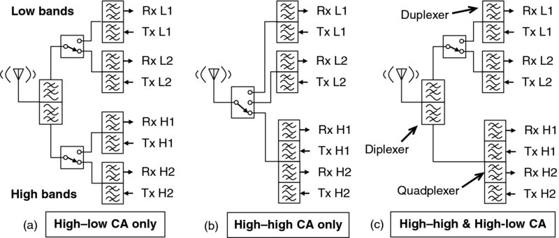
Figure 14.11 (a): Duplexer bank, high–low band switches, diplexer solution, (b): quadplexer, antenna switch solution, (c): duplexer, quadplexer, switch, diplexer solution
Figure 14.11a uses a common diplexer to all bands and supports only high–low CA, for example band 1–band 8, or band 2–band 5. The main drawback of this approach is that bands and air interfaces which are not meant to be used in Carrier Aggregation pay an insertion-loss penalty in both uplink and downlink. The use of a quadplexer in Figure 14.11b considerably simplifies the front-end circuitry, since only one antenna switch is required, and each band of operation benefits from a removal of the diplexer. In this example, only a high–high CA is supported, for example band 2–band 4. Figure 14.11c supports both high–high and high–low CA, but the price that must be paid for this extra capability is that of adding a diplexer. Note that this latter configuration also supports triple-band CA at no or little extra cost compared to the dual-CA solution (a). For example, solution (c) could support inter-band triple band CA of bands 2–4–13. It can be seen that with CA, a variety of front-end architectures must be assessed to deliver the optimum cost/performance tradeoff. For each combination, a tradeoff must be found between complexity and performance. These tradeoffs have generated many discussions at 3GPP on ways to determine the insertion loss associated with each configuration, and how these extra losses should be taken into consideration to define reference sensitivity and maximum output power relaxations. As a consequence, for each dual downlink CA scenario, many filter manufacturers' data had to be collected to agree upon an average insertion loss per type of multiplexer. Further complication occurs since insertion losses are heavily design dependent, as well as band, temperature, and process dependent. An example of the tedious and hard-fought agreements can be found in [16].
14.1.3.2 Power Amplifiers
Power amplifiers are no exception to the design constraints and tradeoffs previously mentioned. With highly integrated single chip transceivers, the RF subsystem area is heavily influenced by the area occupied by FE components and in particular PAs. The ideal solution would call for a unique PA which could be reconfigured to support all bands and all air interface standards. In practice, two approaches are taken to deliver the best compromise between performance and cost: discrete architectures based either on several single-band PAs, or the use of a MMMB PA architecture complemented by a few single-band PAs.
In discrete PA architectures, the most common solution uses a quad-band EGPRS (QBE) power amplifier module (PAM) and dedicated single-band PAs for each WCDMA/LTE band. When the band is common to both WCDMA and LTE, a unique PA is used for both modes, usually with different linearity settings to accommodate the slightly higher PAPR of LTE transmissions.
In MMMB PA architectures, a single triple-mode PAM replaces the QBE PAM, and some of the WCDMA/LTE single-band PAs. Yet, certain LTE specific bands, such as band 7, are not yet covered by MMMB PAM and therefore require a dedicated single-band PA. Examples of implementations of the two approaches are presented in Figure 14.15: solutions 1 and 3 are discrete architectures; solution 2 uses a MMMB PAM complemented by two single-band PAs (band 4 and band 17).
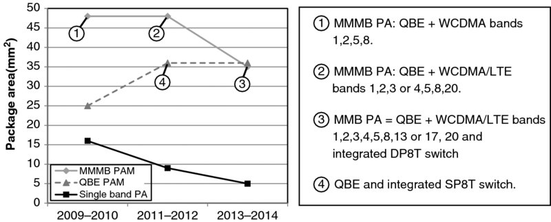
Figure 14.12 PA package size evolution and number of integrated bands – compiled from major suppliers' public domain data
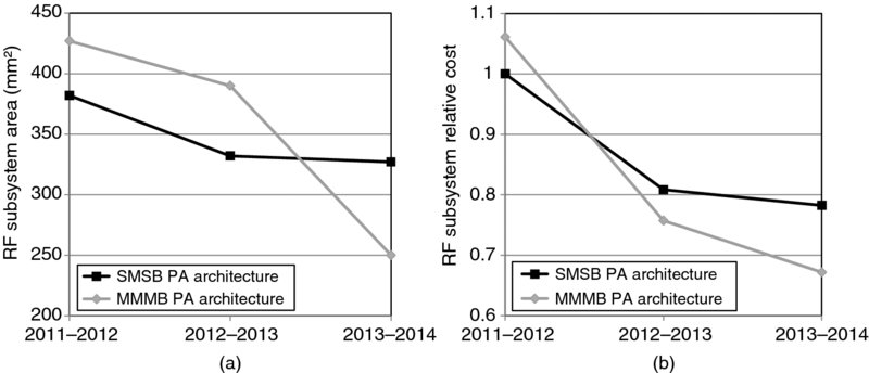
Figure 14.13 Single band vs. MM-MB PAs: RF subsystem area (a) and cost (b) tradeoffs in a NA triple-mode application
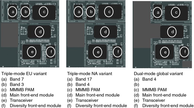
Figure 14.14 Reconfigurability concept with MMMB PA architecture. MMMB PAM covers quad-band EGPRS, penta band 1, 2, 5, 8, 20 in WCDMA and LTE modes [17]. Triple-mode NA variant: QBE, WCDMA I, II, IV, V, VIII, LTE 1, 2, 4, 5, 8, 17, triple-mode European (EU) variant: QBE, WCDMA I, II, IV, V, VIII, LTE 1, 2, 3, 5, 7, 8, 20, WW dual-mode variant: QBE, WCDMA I, II, IV, V, VIII. Renesas 2012 [17]. Reproduced with permission of Renesas Mobile Corporation
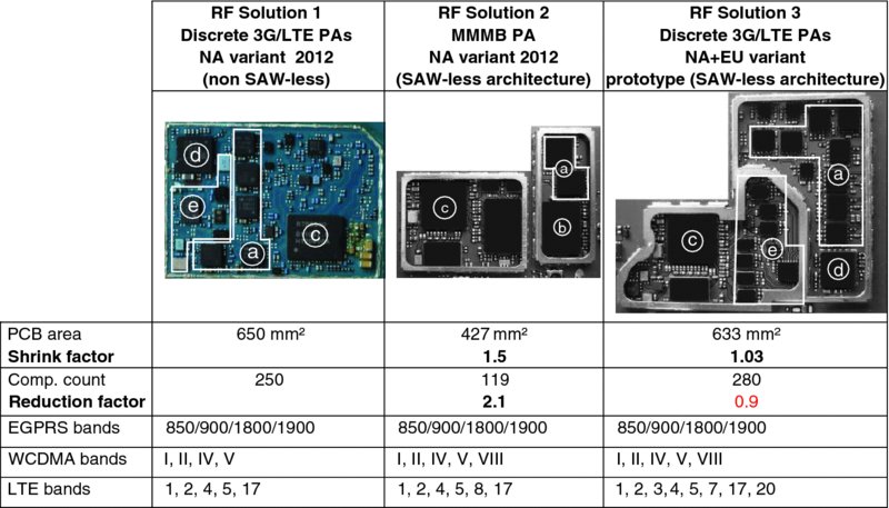
Figure 14.15 Examples of triple-mode RF solutions (discrete and MMMB) – (a) Single-Band PAs (3 × 3 mm), (b) MMMB PAM (5 × 7 mm), (c) Triple-mode transceiver IC, (d) 2.5G Quad-band amplifier module (5 × 5 mm), (e) Duplexers (2.0 × 2.5 mm and 2.0 × 1.6 mm) + antenna switch
The evolution of PA package area (L*W in mm2) over the last 4–5 years is shown in Figure 14.12 for three families: single-band, QBE PAM, and MMMB PAMs.
Single-band PAs (squares) have reduced their footprint by a factor 3, from about 16 mm2 to about 5 mm2. This category has reached a maturity plateau and future packaging technology improvements are unlikely to significantly impact the overall radio area. With 25 mm2 package area, and their long history of production and optimization, QBE PAM (triangles) have also reached a level of maturity and will most likely remain at this level for the coming years. The recent increase in area to 36 mm2 is due to the integration of an SP8T antenna switch. The initial 2009–2010 MMMB PAMs (diamonds) combined a QBE and support for quad-band WCDMA operation. They rapidly evolved to support dual-mode penta-band, and the triple-mode operation octa-band operation. Remarkably, the 2013–2014 MMMB PAM, which covers QBE, octa-band WCDMA/LTE PAM, and a DP8T band distribution switch comes in a package size comparable (35 mm2) to that of a QBE–SP8T module. It is expected that PA suppliers will invest further efforts into these solutions as triple-mode will soon become a de facto requirement.
The choice of architecture is primarily driven by the tradeoff between cost and size for a given band-set. The vast majority of dual-mode EGPRS-WCDMA terminals support two or three WCDMA bands. In these solutions, the discrete PA architecture is often the most preferred solution as there is little or no cost advantage to using a MMMB PAM. An MMMB PAM becomes advantageous when there are four or more WCDMA/LTE bands to be supported. An example of cost tradeoff selection metrics is shown in Figure 14.13 in the specific case of a North America (NA), triple-mode product12. Over time, the MMMB PA architecture is expected to provide both size and cost benefits over the discrete PA architecture. From an RF subsystem PCB area perspective, it requires an octa-band MMMB PAM to better the discrete PA solution. From a cost perspective, the dynamics are less trivial as the introduction of such highly integrated products often benefits from a positive spiral effect: the introduction of a smaller package with increased band coverage induces a cost reduction, which induces a production volume increase, which in itself induces a reduction in sales price.
Several other factors come into play when making a selection of architecture:
- – Power consumption: single-band PAs exhibit better power consumption than MMMB PAMs. This is mainly because discrete PA matching networks can be optimized for a narrow frequency range while MMMB PAMs must be matched over a wider band. In addition, MMMB PAM efficiency is lower as they absorb the insertion losses of the band distribution switch,
- – Design effort: MMMB PAMs considerably simplify the PCB place and route task, especially in variants covering a large number of bands. An example of complexity in attempting to cover a future NA-EU variant using discrete PAs is shown for illustration purposes in Figure 14.15.
- – Multiple vendor sourcing management: MMMB PAMs bring a significant advantage over discrete solutions as they reduce the number of references for a terminal model/variant,
- – Ease of reconfigurability: MMMB PAMs, complemented with one or two single-band PAs, provide the best tradeoff today between cost, PCB place and route complexity, area, and ease of reconfiguration to support multiple ecosystems. An illustration of the reconfigurability concept is shown in Figure 14.14 [17], where a MMMB PAM is used to cover QBE and quad-band WCDMA (I, II, V, VIII) and LTE band 20. This example shows that a single reference design may be quickly adapted to serve three different regions of the world with minimal changes, and yet can achieve rather aggressive, and nearly identical, PCB area and component count metrics.
Finally, Figure 14.15 summarizes all of the previous discussions in one place. RF solutions 1 and 2 address the same NA, triple-mode telecom operator variant and illustrate both graphically and quantitatively the significant gains that MMMB PAMs bring to such products: the area is reduced by 150%, and uses half the components. Solution 3 is a prototype which uses single-band PAs and a QBE PAM to target a NA and EU variant in triple-mode operation. In comparison with solution 1, one can see that this PCB is extremely well-optimized, and it covers three additional LTE and one extra WCDMA band with nearly identical PCB metrics. Yet, it is easy to note that the complexity and the cost associated with such architecture would most likely be unacceptable for OEMs. It is evident from this prototype that next-generation variants which attempt to target more than one ecosystem, such as this effort for NA-EU coverage, can only be cost effective through the use of MMMB PAMs. It is estimated that in this example, the use of the latest octa-band MMMB PAM (Figure 14.12, 2013–2014) could save 7 out of the 8 single-band PAs, with band 7 being the only band which would need a dedicated PA. It thus comes as no surprise that the focus for future PA design will almost surely target the use of MMMB modules.
14.1.3.3 Over-the-Air (OTA) Performance
While chip set suppliers are benchmarked by OEMs to deliver the best RF performance in conducted test conditions, and often have to iterate a design to improve performance by a fraction of a dB, telecom operators, on the other hand, are primarily interested in OTA performance. Between these, the OEMs are more concerned with ensuring their products will pass the impressive set of 3GPP/PTCRB/GCF tests. Typically, the test plan of a triple-mode phone involves approximately 1500 tests, the majority of which are conducted tests, and which typically lead to several months of costly testing. When it comes to OTA performance, the dual-mode EGPRS/HSPA UE is measured against two simple Figures of Merit (FOM)13: Total Radiated Power (TRP) and Total Isotropic Sensitivity (TIS). Each FOM is then re-measured in different user interaction (UI) scenarios: UE in Free Space (FS), held in a hand phantom14, placed against a head phantom or held in hand and placed against the head phantom [18]. Figure 14.16 plots the WCDMA TRP vs. TIS performance, in band V and band II, across a sample of 30 class 3 recently PTCRB-certified smartphones. Looking at the conducted results (circles), UEs generally perform within 1 or 2 dB from each other in both axes. In output power, performance ranges across the class 3 tolerances (24 dBm +1/−3 dB), the majority being calibrated to deliver 23 dBm. In sensitivity, all UEs pass with a comfortable margin, but because this metric is used by OEMs to benchmark chip set platforms, the performance spread is much tighter than in TX power. With OTA TRP and TIS, the spread across UI increases dramatically between bands.
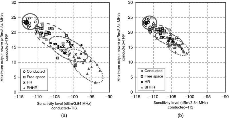
Figure 14.16 Example of modern WCDMA OTA TRP vs. TIS performance of 30 recent smartphones extracted from PTCRB reports based on CTIA OTA test plan. (a): band V mid-channel, (b): band II mid-channel. (HR: Phantom Hand Right only, BHHR: Beside Head and Hand Right Side, that is, head and hand). These graphs compiled with permission of PTCRB
For example, in band V the spread between conducted and BHHR varies between 10 and 18 dB. But in band II, the spread is nearly half that of band V, ranging from 5 to 9 dB in both TRP/TIS. In a given band, the difference between conducted and FS gives a good indication of antenna gain, with superior performance in band II as compared to that in band V. This illustrates that designing an antenna with desired performance in low bands is a significant challenge in modern smartphones. Figure 14.17b, shows that the task of the antenna designer is not becoming any easier, since the volume made available is continually reduced. Because of these constraints, it is not unusual for antennae to reach alarming VSWR values as high 10 : 1, corresponding to mismatch losses (ML) of 4.8 dB. This loss impacts TRP and TIS. One can see that with chip sets no longer being loaded/sourced with the ideal 50 Ohm of the conducted tests, the 0 dBi antenna gain assumption made in 3GPP is far from being met in actual situations.
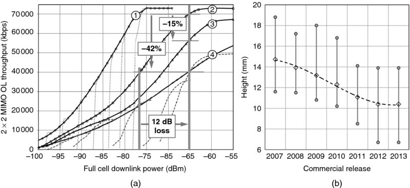
Figure 14.17 (a): example of MIMO throughput loss vs. antenna correlation:  Static bypassed RF channel,
  Low correlation EPA model,
  Medium correlation EPA model,
  High correlation EPA model, (b): trends in smartphones heights. Reproduced with permission of Videotron Ltd.
With user interaction, absorption losses (AL), due to the proximity of body tissues, further degrade antenna performance. Absorption losses depend on grip tightness [19] or on the gap between the UE and the human body, with the hand-only test case usually presenting the lowest loss.
Antenna design becomes further complicated for LTE, since devices must then operate over a wider range of frequencies, from the new ultra-high 2600 MHz band to the ultra-low UHF bands (700–800 MHz) at the lower end of the spectrum [15]. The traditional way to optimize matching, which normally consisted of using a single matching network to deliver the best gain over such a large range thus becomes much more difficult to achieve. These constraints have pushed the industry to look into solutions that enable antenna reconfigurability or antenna tuning capabilities. Two approaches are currently being investigated: one is of antenna-tuners connected to a non-tuneable antenna, and the other is antenna tuners associated to antennae with tuneable resonators. Antenna tuners basically consist of a digitally tuneable impedance matching network. Tuners deliver variable reactances by using an array of switched capacitors and fixed inductors often arranged in a pi topology. The digital settings which optimize performance for each band can be pre-calibrated using look-up tables. However, the best agility is accomplished by using a coupler at the antenna port, so real-time VSWR can be monitored and used in a closed-loop operation to continuously deliver optimal performance, independent of UI. In this respect, the advantage of standardizing an RF-FE digital control bus, such as MIPI® RFFE, allows multiple vendors to be easily interchanged (cf. Section 14.1.3.4). In theory, an antenna tuner should aim at delivering close to 50 Ohm impedance. In practice, depending on the band and antenna structure, the tuner will only be able to partially correct mismatch losses. For example, the study on the impact of grip style in [19] indicates that in most configurations performance is largely dominated by absorption losses, with values ranging from 1.5 to 7 dB loss, while impedance MLs only account for 0.5 to 2.5 dB. In this example an antenna tuner connected to a non-tuneable antenna would not bring significant gains. These moderate gains must be weighed against design challenges associated with front-end circuitry. The linearity requirements for components are high15 [20], and yet components must deliver minimal losses while meeting the low cost and low PCB footprint targets. This is one of the primary reasons why the industry is looking at ways to improve radiated efficiency by developing tuneable antennae. If the antenna is capable of tuning its resonators to the band of operation, then theoretically it should be possible to deliver enhanced antenna efficiency. In this case, antenna tuners become mandatory since the resonator tuning process induces impedance mismatches. Looking further ahead, some companies are also investigating ways of solving AL degradation by designing antennae with preset radiation patterns. With the set of proximity sensors embedded in modern smartphones, one could imagine a phone capable enough to adapt the antenna tuners based upon proximity detection of the user. At this time it is difficult to assess which technique will be the most promising. Some of the most advanced techniques in mass production today rely on antenna selection switching, with or without limited impedance tuning. This technique consists of replacing the diversity receive antenna with an antenna capable of supporting both transmit and receive frequency bands. In this case the platform may swap the primary and diversity antennae at any time so as to maximize system performance. Note that this scheme will not be applicable to future platforms needing to support transmit diversity.
With MIMO LTE, downlink throughput is the new FOM. MIMO throughput depends on the end-to-end correlation between the two data streams. Consequently, the UE demodulator experiences the product of three matrices: eNodeB TX antennae, RF propagation channel, and UE RX antennae correlation matrix.
Figure 14.17a, shows the impact of the RF channel correlation matrix on a recent triple-mode UE in a conducted test setup. The measurement is performed in AWS band, 10 MHz cell BW, using a 2 × 2 MIMO RF multipath fader. The graph plots UE DL throughput measured by an Anritsu 8820c eNodeB emulator vs. DL full cell BW power under four RF propagation conditions: static bypass mode (dots), low (squares), mid (triangles), and high (crosses) correlation matrices of the 3GPP EPA fading model. For each RF fading model, the DL MCS index is varied to capture the UE behavior across its entire range of demodulation capabilities. To avoid overloading the figure, only a few waterfall curves are shown in light gray dotted lines. The resulting envelope of each waterfall is plotted in plain lines.
This graph provides insights into the susceptibility of LTE MIMO performance to correlation. There are two ways to read this experimental data:
- Case of a user located under an eNodeB, experiencing a high DL RF power of, say, −65 dBm. The difference between low vs. mid, and low vs. high correlation results in a 19% and 42% throughput loss, respectively. In the latter case, the throughput drops from 70 Mbit/s to about 40 Mbit/s. Under high correlation conditions, the impairment is so bad that the BB is unable to deliver more than 54 Mbit/s even at maximum input power (not shown on graph). From a user experience perspective, it is unlikely that this lower-than-expected performance would be noticed, since absolute throughput is not a sufficient metric to guarantee a good user experience (see Chapter 13 for more details). From a telecom operator's perspective, the situation is quite different as this loss prevents the cell from delivering the maximum theoretical performance.
- At a given target throughput, increasing correlation leads to a degraded UE RF sensitivity. For example, at a target 40 Mbit/s, a user experiencing high correlation suffers from a 12 dB penalty in link budget. This penalty increases with increasing target throughput because of the floor in performance of that particular test case. This graph can also be interpreted as a fair illustration of the differences one can expect between operation in high bands (e.g., 2600 MHz) where the antenna should perform well, and low band operation (e.g. 700 MHz). Note that at cell edge, in low SNR conditions, there is little difference in performance.
This graph shows how crucial it is for telecom operators to jointly define with 3GPP a standardized OTA test method. In an ideal world, OTA testing should be able to reproduce and predict field performance. In practice, predicting OTA MIMO user experience appears to be a nearly impossible task because so many variables can impact performance. At worst, OTA testing will deliver a reliable tool to benchmark terminals against one other. Here are a few examples of the challenges – based on recent contributions:
- Contribution [21] has shown that antenna correlation in a smartphone is so sensitive to its close surroundings that the presence of tiny co-axial semi-rigid cables impacts the measurement accuracy. Using optical fiber feeds, FS correlation reached 0.8, a high value, while measurements with semi-rigid feeds indicated a correlation on the order of 0.4. If tiny semi-rigid cables can change the correlation by a factor of two, it is reasonable to assume that the presence of larger objects could induce greater impairments. Unfortunately, the nature of interactions is so complex that no general rule governing the degradation of antenna correlation can be drawn. For example, the study in [22] shows that a smartphone with good FS performance can turn into a poor terminal in the presence of a human body – but the exact opposite is also true. The study in [23] goes a step further by measuring the impact of a real user on antenna correlation vs. FS and phantom head. The study uses prototypes specifically designed to deliver high and low correlation performance in the 700 and 2600 MHz bands. Measurements demonstrate that the difference between high and low correlation decreases with UI, so much so that at 700 MHz, it becomes difficult to distinguish the two prototypes in the presence of a real person. This suggests that any ranking between good and bad devices based on FS and phantom head measurements might not be in agreement with the more subjective rankings resulting from actual use (see also [24]).
- In addition, antenna correlation varies vs. carrier frequency in a given band.
- From the above results, it may be intuitively understood that the angle of arrival also plays an important role. For example, one may expect that the use of phantom head only might not block as many incident waves as would be blocked by real person. This implies that measuring user experience requires a 3D isotropic test setup. 3GPP is assessing three test methods that could fulfill this requirement: anechoic, reverberation chambers, and a two-stage method. With their intrinsic 3D isotropic properties, reverberation chambers are an attractive solution to this problem.
- Another difference between lab measurements and practical user experience is that 3GPP test cases do not include closed-loop interactions between a NodeB and UE. Good MIMO performance is about making the best of the instantaneous radio conditions, either by using frequency selective scheduling or by adapting rank. These closed-loop algorithms are proprietary to each network equipment vendor and cannot be replicated using eNodeB emulators.
These are some of the complex challenges that OEMs, telecom operators, and chip set vendors are currently facing when it comes to defining OTA performance test cases. Not only must 3GPP assess and recommend test methods (AC, RC, or two-stage) but it must also define test conditions and pass/fail criteria to provide operators with a reliable and realistic tool to benchmark devices. Considering the complexity of the interactions between UE antennae and the surroundings, this task is far from trivial.
14.1.3.4 RF Subsystem Control and IQ Interfaces
The conventional RF subsystem architecture relies on analog IQ RF-BB interfaces and a myriad of control interfaces specific to each of the RF-FE components. The primary disadvantages of this approach are twofold:
- – The associated number of pins tends to be larger, which increases package size, cost, and further complicates PCB routing.
- – Dealing with a wide variety of proprietary interfaces restricts the ease with which handset makers can “mix and match” RF-FE components, and often leads to software segmentation.
The example in Figure 14.18 shows a hypothetical downlink-only carrier aggregation RF subsystem focusing on control and IQ interfaces only. In total, 47 pins are required. This number depends on the choice of ICs, such as the type of power amplifier, the number of bands and antennae that are selected for a given handset variant.
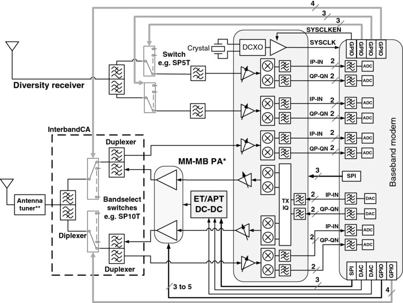
Figure 14.18 LTE inter-band carrier aggregation hypothetical block diagram using conventional buses. Pin count: 14 (switches) +20 (IQ) + 8 (PA-CTL) + 3 (SPI) + 2 (sysclk) = 47 pins. Interconnect for MM-MB PA temperature sensor (*), and antenna directional coupler (**) not included. For illustration purposes only. Pin count required for RF switch control could be reduced by sharing one or several sets of GPIO lines
The MIPI Alliance16 RFFE and DigRF v4 digital interfaces have been designed to specifically address these issues. DigRF v4 offers features and capabilities specifically designed for BBIC-RFIC bidirectional exchange of both data and control. With 1.248 GBit/s minimum bus speed, DigRF v4 is a high speed, low voltage swing, point-to-point digital interface. It provides numerous flexible options for implementers, such that aspects like pin count, spectral emissions, power consumption, and other parameters may be optimized for various operating conditions imposed by a given design. While these interface options allow for tradeoffs to be made in a current design, they also provide adaptive growth potential for new services, such as carrier aggregation, without undue modifications to either the interface specification or to existing Intellectual Property (IP) used for building implementations. DigRF uses a minimum of seven pins: a pair of differential lines for RX and a pair for TX with both carrying IQ data and control/status information, a reference clock pin (RefClk), a reference clock enable pin (RefClkEn), and a DigRF interface enable pin (DigRFEn).
The Radio Frequency Front-End Control Interface Specification, or RFFE as it is commonly known, has emerged in recent years as the de facto standard for implementing RF front-end control. Even though other digital control interfaces might provide some of the basic functionality required, RFFE has been designed to address specific needs that are frequently presented, or are increasingly desired, in modern UEs. A single RFFE bus instance supports a single master, along with up to 15 slave devices connected in a point-to-multipoint configuration. Comparatively, RFFE is a low speed, high voltage-swing interface. The master, or major controlling entity for an RFFE interface instantiation, may be hosted within an RFIC, or in some other component such as a BBIC or other device which is suitable for the slightly higher level of integration required for an RFFE controller. An RFFE bus uses three pins: a unidirectional clock line driven by the master (SCLK), a common unidirectional (optionally bidirectional) data line called SDATA, and a common line for voltage referencing, and optionally for supply, called VIO. Some of the high-level characteristics for each of these interfaces are summarized in Table 14.1.
Table 14.1 Selected DigRF v4 and RFFE characteristics. DigRF clock frequencies (*) assume a 26 MHz reference crystal oscillator. DigRFv4 has defined a set of alternate clock frequencies associated with 19.2MHz crystal reference oscillators
| DigRF v4 | RFFE | |
| Point-to-Point | Point-to-Multipoint | |
| Bus topology | Transceiver ↔ Baseband | Transceiver or Baseband → RF-FE |
| Termination | Terminated or unterminated | Unterminated |
| Voltage swing | 100 to 200 mV pk-pk differential | 1.8 or 1.2 V single-ended |
| Clock frequencies | 1248, 1456, 2496, 2912, 4992, 5824* MHz | 32 kHz to 26 MHz |
| Pin count | Minimum 7 pins | 3 pins |
Figure 14.19 shows that applying both interfaces to the example of Figure 14.18 may save up to 32 pins. Note that the system partitioning is implementation-specific and Figure 14.19 is only presented to illustrate cost/pin savings. If the RF IC is already pin count limited, it might be decided to “host” some, or all, of the RFFE buses either in the BBIC or in the PMIC.
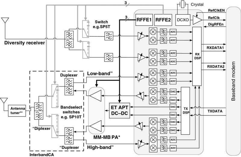
Figure 14.19 LTE inter-band carrier aggregation hypothetical block diagram using DigRF and RFFE. Assumes DigRF v4 is clocked at 2496 MHz, assumes a separate RFFE bus for switches and for PA control. Interconnect for MM-MB PA temperature sensor (*), and antenna directional coupler (**) not included.9 (DigRF) + 6 (RFFE) = 15 pins
Beyond these direct hardware savings, both interfaces provide additional advantages which can be of benefit to both component suppliers and platform designers.
With DigRF, IQ ADCs and DACs are located in the RF TRX. The BB IC may then become a pure digital IC, which helps in decoupling the CMOS node used in each IC. The BB may then be shrunk/ported to the latest CMOS node more easily, while the RF transceiver can remain in an “older” CMOS node which offers a more appropriate performance/cost/power consumption tradeoff specific to the needs of the RF IC. This is particularly important as the latest, most advanced CMOS nodes rarely offer the design libraries required to simulate and design all portions of the complex RF transceiver. Further, the DigRF interface was also defined to assist handset makers to interface RF ICs and BB ICs from different suppliers, which allows more flexibility in component selection. DigRF also provides a standardized and low pin count debug interface to monitor traffic at the IQ interface. Indeed, a number of well-known test equipment providers distribute systems to enable this capability. For chip set makers, DigRF v4 is built upon MIPI's M-PHY, a physical layer IP which, once developed for DigRF, may be reused for other protocols and applications, since an increasing number of applicable standards use the M-PHY physical layer. IP reuse is increasingly important in meeting tough time-to-market deadlines. For example, future generations of DDR memories could make use of M-PHY, and an existing standard for FLASH already leverages M-PHY.
For RF front-end components, the current situation with regards to the types, numbers, and suppliers of these is perhaps even more diverse and far-reaching. To handset makers, RFFE is a tool which considerably simplifies the selection, ease of integration, and swapping of RF-FE components. To RF-FE IC makers, it offers increased opportunities to integrate with many chip set platforms, while implementing a single, widely-deployed control interface. With a wide array of optional features, particularly for slaves, this ensures that a bus and, in particular, the FE components may be optimized for the features implemented vs. cost and the implementation technology. RFFE's wide scope of applicability to FEMs provides increased potential for IP reuse of hardware and/or software.
As with any interfaces deployed in an RF-sensitive area, one must pay special attention to the issues of EMI/co-existence management. The specifics of each of these interfaces leads to different co-existence challenges. The main issue with DigRF v4 in this respect is that even at its lowest operating clock frequency of 1248 MHz, the first spectrum lobe of a pair of lanes overlaps all UHF cellular frequency bands. At 2496 MHz, it is nearly the entire set of 3GPP operating bands which fall under the first lobe. In addition, with high duty cycle operation for standards such as LTE, the probability of collision in the time domain is high. For example, in the case of LTE single carrier 20 MHz operation, the load of a single RX pair of lanes ranges from 137% at 1248 MHz (and thus requires two pairs of lanes) to 67% at 2496 MHz using one lane pair [5]. The inherent flat decay of the common mode PSD also poses some threats to differential LNA input structures. Factors which tend to help in reducing co-existence issues are that the interface may be operated using low voltage swings, in a controlled transmission impedance, and with bus routing that in most handset designs is unlikely to be routed at, or near, the sensitive front-end components such as antennae. RF transceiver pin-to-pin isolation is therefore the main coupling mechanism.
With RFFE being a control interface only, the bus load is often bursty, with only rare instances where higher bus loading might be required. Therefore, the probability of collision in the time domain is lowered. In addition, its relatively low frequency range of operation (32 kHz to 26 MHz) is such that even the lowest cellular frequency bands, such as the LTE 700 MHz bands, are located at the 28th and 22 500th harmonic of the extreme interface rates of 26 MHz and 32 kHz, respectively. This provides plenty of “room” to implement spectrally efficient pulse shaping techniques. Yet, in contrast to DigRF, RFFE voltage swing is higher, and its point-to-multipoint topology can lead to longer PCB traces, some of which may be routed close to sensitive front-end components. Further, since the bus is not designed to be terminated, its impedance is more difficult to control, and any reflections will tend to impair the decay of spectral lobes. Because PSD decays slowly at high harmonic numbers, and pin-to-pin isolation decreases as operating frequency increases, RFFE co-existence issues may dominate above 1 GHz of operation. The most sensitive victim of this may be GPS, which requires aggressor noise PSD < −180 dBm/Hz to prevent less than 0.2 dB desense.
To help both chip set vendors and handset makers foresee co-existence issues in the early phase of product development, and to prepare for them, both DigRF and RFFE working groups anticipated the need to include a set of EMI mitigation tools. These unique features provide a rich, efficient, and yet relatively simple-to-implement set of techniques for reducing the associated impacts in the frequency and the power domains.
- Pulse shaping/slew rate control: Perhaps the most efficient of all EMI tools made available to handset makers. This feature allows shaping of the rising and falling edges of each transmitted bit so as to reduce the power spectral density (PSD) of the digital bit stream. This is available in both DigRF [5] and in RFFE.
- Amplitude control: A simple and yet efficient way of reducing the aggressor PSD. This option is available in DigRF, and also to a certain extent in RFFE, where 1.2 V is also specified in addition to 1.8 V.
- Clock dithering: A useful feature in cases when repetitive and frequent transmissions of a given pulse pattern generate discrete spurs colliding with a cellular victim. This can be the case, for example, for the DigRF training sequence transmitted at the beginning of each burst to ease clock recovery. This tool is available as a part of the DigRF specification. It is also inherent in RFFE, where the master clock may be dithered between messages, since the clock used for control information need not be related to RF data. Also in RFFE, the timing between messages may be randomized, offering some ability to affect the “signature” for both clock and data streams.
- Alternate clock frequency: This feature is available in both interfaces and can be used to either place the victim in the vicinity of a spectral “zero” or “null,” or by placing the victim under a higher order spectral lobe. For example, in DigRF v4, if GPS RX is desensitized when the bus is operated at 1248 MHz, the alternate clock rate of 1496 MHz places the GPS RX in close proximity of the first DigRF spectral null. In this instance, the aggressor PSD is significantly reduced with minimal impact on DigRF performance. In RFFE the extent of any harmonics is relatively narrow, and a slight change in the fundamental may often be utilized to move a resultant spike away from a specific band frequency of interest.
With the increasing need for more reconfigurable RF subsystems, and the mounting complexity in RF-FEs, these interfaces offer handset designers effective means for the solution of complex challenges. The ability to tailor them to specific needs provides component suppliers with an efficient method to achieve faster design cycles and to foster reuse. And, because EMI effects have been taken into consideration from the outset, these interfaces provide features well-suited to the goals and situations of all those involved in UE design. The DigRF interface will be adding 4998 MHz operation as a means to extend applicability to the future higher bandwidth requirements of carrier aggregation. And work is underway on RFFE to further enhance interface throughput, which will help to improve critical timing, and provide even more bandwidth for increasingly complex RF-FEs. Thus both of these interfaces offer continued promise for the future of handset design through cost minimization and complexity reduction, while also maximizing business opportunities.
14.1.3.5 Co-Existence Challenges
The principles of co-existence have been introduced in Section 14.1.2, where due to the full duplex nature of WCDMA, a UE located at cell edge may be desensitized due to its own transmitter being operated at maximum output power. In this relatively simple example, solutions range from the use of external SAW filters, to novel RF TRX architectures, and in the most challenging cases to 3GPP relaxations.
Co-existence issues become significantly more complex when multiple radios start to interact with each other, or when a radio is operated in the presence of internal jammers that are not enabled during conformance tests. For example, WCDMA receiver sensitivity may be impacted by USB high speed harmonics during a UE to external PC media transfer. In SoCs, aggressors range from simple clock harmonics, to noisy high speed digital buses associated with DSP, CPUs, camera and display interfaces, high current rating DC–DC converters, USB and HDMi ports. As for victims, nearly all RF subsystems are susceptible to EMI interference. Further complexity arises from the fact that RF transmitter chains are not exempt from becoming victims of these digital aggressors. Desensitization occurs when aggressors collide with victims in time, frequency, and power domains. In SoCs, both conducted and electromagnetic coupling may occur. The WCDMA UE RF self-desense is one example of conducted coupling. Coupling via power supply rails and/or ground currents is another. Electromagnetic coupling may occur via pin-to-pin interactions, bonding wires, PCB track-to-track, and even antenna-to-antenna coupling. Problems are exacerbated when collisions occur between the cellular and the connectivity radios. For example, the third harmonics of band 5 fall into WLAN 2.4 GHz, while the WLAN 5 GHz receiver might become victim of either band 2, or band 4 third harmonics, or band 5 seventh harmonics. The number of scenarios may become so great that co-existence studies often have to be performed using a multidimensional systems analysis. This topic constitutes an excellent playing field for innovative mitigation techniques, which commonly fall into two categories:
- Improve victim's immunity by increasing isolation in all possible domains: floor plan optimization, careful PCB layout, the use of RF and power supply filters as well as RF shielding. Victims may also be protected by ensuring non-concurrent operations in time.
- Reduce the aggressor signal level. Slew rate and voltage swing control are two of the most efficient techniques to reduce the level of interference at RF. Slew rate control consists in shaping the rising and falling edges of digital signals. This results in an equivalent low-pass filtering of the digital signal high-frequency content, and therefore helps to reduce the aggressor power spectral density in the victim's bands. For example, DigRFSMv4 line drivers are equipped with slew rate control as a tool to reduce EMI. Frequency evasion is another commonly used technique [25]. For example, if the harmonic of a digital clock is identified as a source of desensitization, it is tempting to slightly alter the clock frequency only when the victim is tuned to the blocked channel. Frequency avoidance can be implemented by either simple frequency offset, or by dithering (e.g., DigRFSMv4, Section 14.1.3.4), frequency hopping, or even by using direct sequence spreading of the clock.
The well-documented example of Band 4 (B4) – Band 17 (B17) carrier aggregation is a good illustration of co-existence issues within the cellular RF subsystem. B17 transmitter chain third harmonics (H3) can entirely overlap the B4 receiver frequency band. Nearly all components in the RF-FE generate B17 H3, with the PA being, of course, the dominant source. It has been shown in [26] that the sole contribution of the PA would cause 36 to 43 dB B4 RX desensitization, therefore calling for the insertion of a harmonic rejection filter. This might not solve the problem entirely since other sources of leakage, such as PCB coupling and TRX pin-to-pin isolation may dominate system performance [27]. Given reasonable PCB isolation and typical component contributions, B4 RX desense should not exceed 7 to 9 dB for 10 MHz and 5 MHz bandwidth operation respectively [28].
14.2 Power Consumption Reduction in Terminals
14.2.1 Smartphone Power Consumption
Poor battery life is probably at the top of the list of criticisms that smartphones face today. Users commonly have to recharge their terminals on a daily basis, and perhaps more often with heavy usage. Such a need clearly affects the user's experience. Figure 14.20 provides some of the factors to help illustrate the current experience. The bar graph on the left plots the evolution of the WCDMA subsystem power consumption for feature phones, compared to a selection of recent smartphones. The measurements are performed with the LCD screen “switched-off,” and at minimum transmit output power, so as to minimize both the impact of the power amplifier and screen-related contributions. Not surprisingly, the trend in power consumption reduction is similar in both families of terminals. It is interesting to note the latest generation of chip sets used in smartphones outperforms even the best cost-optimized solution of the recent feature phones. For example, phone F consumes nearly twice as much as smartphone J.
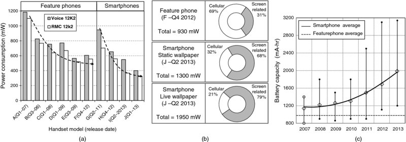
Figure 14.20 (a): screen “OFF,” WCDMA power consumption at minimum output power (−50 dBm), (b): Screen “ON” brightness at 50% level, WCDMA power consumption integrated over TS09 profile, (c): Battery capacity trends vs. year: feature phone average (dashed-line), smartphone average (plain line)
The pie charts in Figure 14.20 show the impact of display-related contributors, such as screen, backlighting, and application engine, on the overall power consumption over the duration of a WCDMA voice call. The voice call consumption is measured according to the GSMA TS09 guidelines. In feature phone F, 70% of the total power consumption is related to the cellular subsystem, while screen-related activities only account for the remaining 30%. In smartphone J, the situation is completely reversed: the “cellular”-“screen-related” contribution split is 30–70%. Despite its state-of-the-art cellular power consumption, the smartphone J total power consumption, particularly when used with a live (or animated) wallpaper, is double that of feature phone F. Feature phones are almost entirely designed with an eye towards communication functions, such as voice calls, SMSs, and MMSs. However, with smartphones, recent user activity statistics [29] show that users spend only 25% of their time making voice calls. The remaining 75% of the user's time is spent on activities such as video streaming, web surfing, gaming, or activities related to entertainment or social networking. Each of these use cases implies heavier screen activity. This serves to explain why the power consumption is so high for smartphones. It also explains why, with nearly 2000 mAh battery capacity (Figure 14.20b), the modern smartphone, with its high resolution displays and more powerful application engine, requires a battery nearly twice as large, and therefore heavier, than the average feature phone. It also helps to understand why, despite this fact, that battery life is still a factor for users. And finally, the split between cellular and screen-related activity also explains why advanced 3GPP battery saving features, such as continuous packet connectivity, with discontinuous reception and transmission (DRX, DTX), have a limited impact on user experience. Section 14.2.2 highlights screen related contributors with a focus on the application engine. Techniques in mass production to improve the cellular power amplifier efficiency are presented in Section 14.2.3. Challenges associated with the implementation of CPC DRX are presented in Section 14.2.4.
With this high dependency on screen content and user activity, the estimation of battery life has become a rather complex task as the UE power consumption should now be assessed over a 24-hour user activity profile. The UE power consumption should then be assessed for each subsystem (WiFi, cellular, BT, FM, GPS), for each activity, and then could be finally averaged for a given customer profile. An example of such a profile can be found in Chapter 13. It is worth noting that, at the time of writing, the CTIA battery ad hoc group has launched an initiative which aims at defining such profiles so that published battery life better reflects the end user experience.
14.2.2 Application Engines
Over the last 15 years, mobile phones have evolved from voice centric, low-resolution, and small display size “feature phones” to data-centric “smartphones.” With their high screen resolution and large size displays, smartphones have considerably improved web browsing and gaming user experience. Figure 14.21 shows that display size has gained on average 1 inch over the last three years, with most devices now using between 4′′ and 6′′ displays. At the same time, display resolution has grown exponentially to reach the full HD resolution of TV screens (1080 p). The growth in screen resolution has been one of the key drivers in the race to deliver more processing power in graphic processor units (GPU) and application engines (APE).
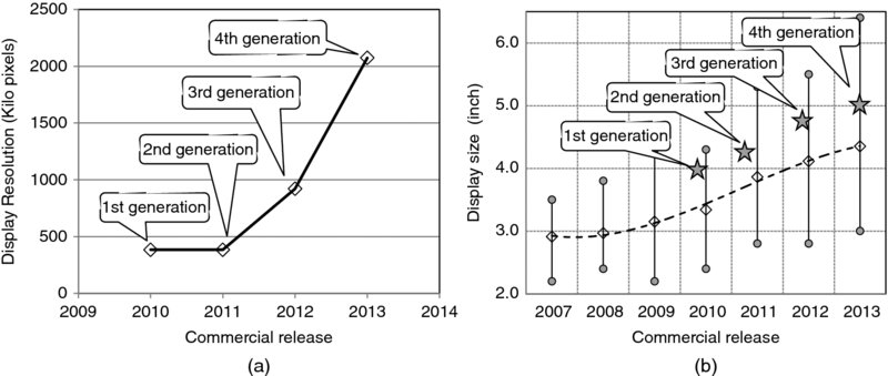
Figure 14.21 (a) Display resolution for four generations of an iconic tier-one smartphone family, (b) Display size trend
As pointed out in Figure 14.20, screen-related activity dramatically increases the UE power consumption. Figure 14.22 provides a detailed breakdown of the “screen-related” contributions vs. use case in a low-end Android smartphone. Camcorder, gaming, and video playback estimations assume flight mode. HSPA+ data and WCDMA voice call assume the UE screen is in “off” state. The HSPA background emulates an email synchronization use case, using a single carrier HSDPA cat 14, HSUPA cat 6, and an animated wallpaper identical to that used in the pie chart in Figure 14.20. Summing all screen-related contributors associated with the animated wallpaper use case, the cellular/screen-power consumption ratio is 40–60% and 32–68% for HSPA background and voice call respectively. Zooming in on the screen-related contributors, the screen and its backlight circuitry consume nearly as much as the whole DC–HSPA+ cellular subsystem. The second biggest contributor is the center of attention in this section: the application engine (APE).
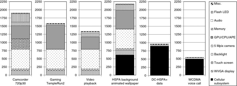
Figure 14.22 Estimated power consumption for a low-end Android 4.1 smartphone: Video playback assumes 1080p at 30 fps. All cellular activity is performed at 0 dBm transmit power. Dual-cell HSPA+ data session assumes 42 Mbit/s downlink, 11 Mbit/s uplink data, HSPA background assumes 21 Mbit/s downlink, 5.6 Mbit/s uplink data. Cellular subsystem= RF sub-system + digital baseband modem
The APE CPU is in charge of two main tasks: general purpose processing and off-loading of computing intensive tasks to the GPU. Both CPU and GPU performance has constantly increased over the last decade. Figure 14.23a shows that in the last three years, the growth has risen exponentially, reaching near 35 000 Dhrystone Mega Instructions Per Second (DMIPS).
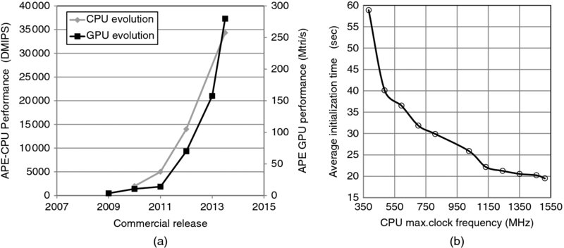
Figure 14.23 (a): CPU and GPU performance evolution over year. (b): TempleRun2 game application load and initialization time vs. CPU performance
Relating user experience to APE processing power is not trivial, as performance experienced by the end user depends on the nature of the tasks required by the application, its mapping to either CPU, GPU, or both, and also the performance of external key components such as the dynamic random access memory (DRAM). For example, Figure 14.23b shows that doubling the CPU performance from 750 to 1500 MHz on an Android dual core CPU platform reduces the loading and initialization time of the Temple Run2 game by only a factor of 1.5. In other words, increasing the CPU/GPU clock frequency does not always result in a linear increase in performance across all use cases. In this simple example, the interface bus speed, Double Data Rate (DDR) DRAM, and IOs (eMMC, μSD) latencies may dominate the APE performance perceived by the end user. The ever-increasing CPU and GPU operating clock frequencies have pushed mobile phone DRAM vendors to reach an unprecedented level of performance. Recent DRAM can sustain transfer rates on the order of 17 GB/s. Despite this impressive level of performance, DDR may, under certain use cases, remain the performance bottleneck above a certain CPU/GPU clock frequency. One illustration is presented in Figure 14.24b which shows that layout Vellamo scores increase linearly with CPU clock frequency. Vellamo is a benchmark tool which measures HTML5 performance and user experience. However, the Ocean zoomer and scroller scores in Figure 14.24a exhibit a performance floor. In this use case, increasing CPU clock frequency above 1 GHz does not significantly improve performance. In summary, user experience depends on many variables: intrinsic DDR, CPU and GPU performance matters, but also the ability of the CPU to efficiently serve the GPU comes into play.
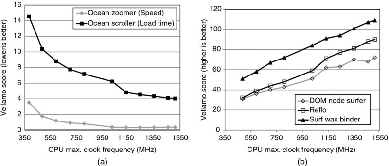
Figure 14.24 (a): Vellamo HTML5 user experience benchmark. (b): Vellamo scripting and layout performance. Both measurements are performed using a high end, dual-core Android smartphone
Finally, user experience is also impacted by the way mobile applications are developed. The trend has evolved from pre-embedded, custom designed applications for a given terminal platform, to the world of online application (market) stores. While it was possible to optimize applications for a certain handset prior to mass production, applications must now be developed for a heterogeneous set of chip sets. The challenge in selecting CPU performance now consists in tailoring the best performance power consumption tradeoff in anticipation of applications that will be created after the handset has been commercialized.
When it comes to increasing APE performance, three techniques are commonly used:
- Increase CPU clock speed. Increasing CPU clock to the 2 GHz mark while keeping power consumption reasonably low has been made possible thanks to the rapid CMOS technology shrink over the last decade. Two key tools have made this achievement feasible: Digital Voltage Frequency Scaling (DVFS) in hardware and Operating Processing Point (OPP) in software.
- Increase CPU pipeline length: this technique improved the DMIPS/MHz performance. In the example of the ARM17® CPU core family, performance has improved from 1.25 DMIPS/MHz for the ARM1176TM to 3.5DMIPS/MHz for the Cortex®-A15 processor.
- Increase the number of cores per CPU. In 2011, the introduction of Multi Processing (MP) capable cores such as the ARM Cortex-A9 MP capable core, together with symmetrical multiprocessing (SMP), enabled parallelizing of software processing on 2 to 4 Cortex®-A9 cores. These recent advances multiply the theoretical maximum performance of the CPU by a factor of 4. Nevertheless, increasing the number of cores only makes sense if the OS kernel and the applications are designed to provide a high level of parallel tasking. Applying Amdahl's law [30] to a quad-core CPU shows that performance gains become negligible if less than 75% of parallelism is effective.
However, this increase in CPU performance comes at the expense of both static and dynamic power consumption. ARM big.LITTLETM processing aims to deliver the best combination of performance and power consumption by pairing two processors in a coherent system. In the first instance a “big” high-performance quad-core Cortex-A15 processor is paired with a “little” energy efficient, quad-core Cortex-A7 processor. The Dhrystone benchmark shows that “little” cores are 3.5 times more energy efficient than the “big” cores, while “big” cores are 1.9 times more powerful. Ideally, demanding tasks would be scheduled on the “big” cores while less-demanding and background tasks would be scheduled on the “little” cores to optimize power consumption.
There are currently three possible modes of operation for ARM big.LITTLETM technology. The simplest approach called the “cluster migration” consists in creating two types of clusters: a cluster made up of a maximum of four “little” cores, and a cluster of up to four “big” cores. The software tasks are then either mapped to one cluster or another. This has the advantage of presenting a homogeneous set of processors to the programmers. The main disadvantage is that, at best, only half of the total number of cores is active.
The second approach, called CPU migration, is slightly more complex. It consists in creating logical pairs made up of one “big” and one “little” physical core. The special case of a quad-core APE is shown in Figure 14.25a. Compared to cluster migration, this solution remains relatively simple to operate as switching between physical cores can be done by the Linux governor using both OPP, DVFS, and CPU cores hot-plugging techniques. The main drawback of the CPU migration approach is that it also uses only half of the available cores. Further, a workload oscillating between low and high performance can lead to user experience degradation. To avoid these oscillations, a hysteresis scheme is often implemented using OPP sticky points. Sticky points serve to maintain task scheduling on a given core type, and a task is migrated only if the required performance load is maintained over a certain period of time. This concept is similar to the scheme used in PA gain-switching, where hysteresis is sometimes used to prevent phase jumps from violating 3GPP requirements (see Section 14.2.3). In this sense, toggling between a “little” and a “big” core is analogous to switching the PA between its high and low power mode. Note that, in the future, nothing precludes pushing the analogy with PA control scheme further by assuming the concept of big.LITTLETM could be extended to adopt a big-middle-little concept, in a fashion similar to the low-mid-high power modes of the cellular power amplifier.
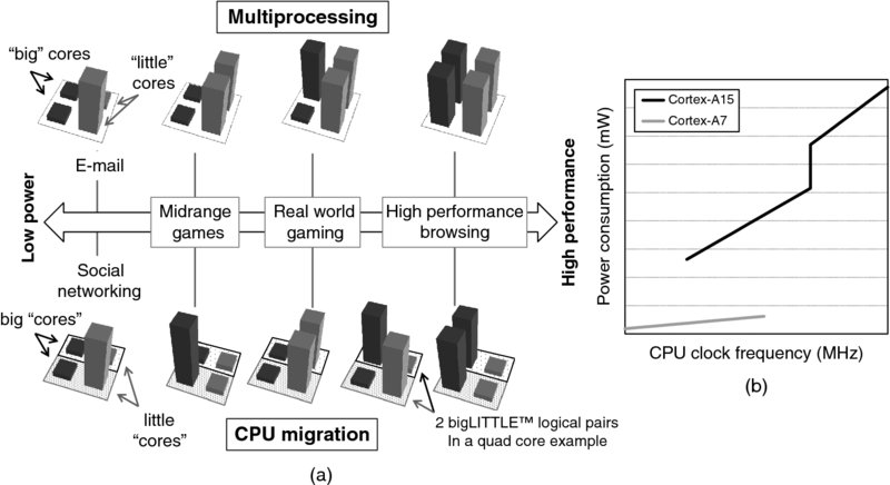
Figure 14.25 (a): ARM big.LITTLETM CPU migration and multiprocessing concepts. (b): consumption vs. frequency vs. cores
The third approach, called “Multi-Processing” (MP), or also global task scheduling, allows all cores, or any combination of cores, to be active simultaneously (Figure 14.25a). As demand for processing power increases, load may be scheduled from one to all cores. The MP approach is more complex but it has the advantage of handling all cores. Its implementation is challenging because the kernel must be aware of task attributes in order to decide to which core the task should be scheduled. The kernel needs to have a good understanding if the task attribute is that of a foreground or background task, and of the amount of CPU load required.
A number of initiatives are currently being studied to make the best use of “big.LITTLETM” processing technologies. Among the more promising candidates is the big.LITTLE MP developed by ARM [31]. The solution allocates small tasks on “little” CPUs, without aggressively packing the tasks on as few CPUs as possible. The solution makes use of the task statistics to predict future task computation load. At the time of writing, big.LITTLE MP has just been released, and consequently early commercial implementations made use of the CPU migration and cluster migration approaches. In the near future, ARM big.LITTLE MP will most likely be the solution of choice since it delivers the best performance/power consumption tradeoff.
Finally, thermal dissipation is another critical aspect that must be considered when employing high performance APEs in the tiny enclosures of the modern smartphone. Transistor current leakage for process nodes such as CMOS 28 nm becomes an important factor at high operating temperatures. The higher the energy drawn by the SoC, the higher the thermal dissipation. In turn, the higher the junction temperature, the higher the current leakage, thereby leading to a positive feedback loop also sometimes referred as “thermal runaway.” This phenomenon is shown in Figure 14.26 and is best illustrated when operating all eight cores at 100% load (four Cortex-A7 and four Cortex-A15). Note that the current increase with temperature tends to adopt a slight exponential curve which will be exacerbated in future CMOS shrinks. Under these circumstances, the system enters a positive feedback loop which eventually may lead to chip destruction. APE thermal monitoring then becomes necessary to stay within the safe thermal envelope of the chip. To give an idea of the power/thermal constraints, it is worth recalling that the APEs can draw up to 4 Amperes peak current.
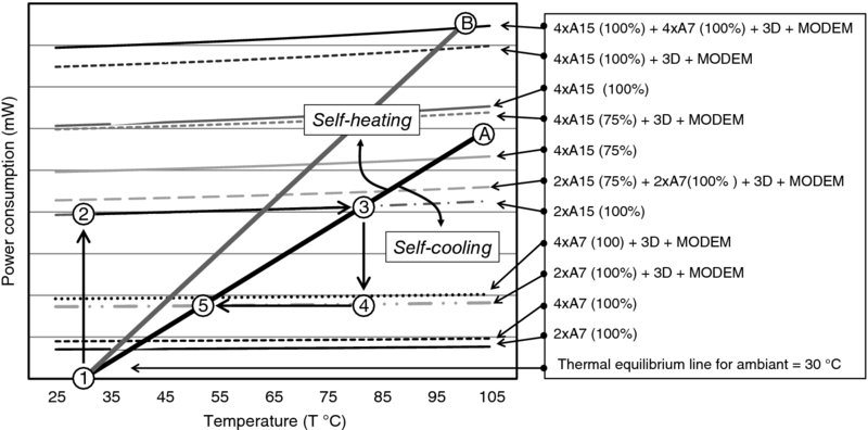
Figure 14.26 Power consumption vs. performance and thermal runaway in a 4 × 4 AMR® big.LITTLETM processor configuration. Thick plain lines A and B are two examples of PCB thermal equilibrium lines: B corresponds to a greater heat sink capability than A
Figure 14.26 plots the battery power consumption of an octa-core ARM® big.LITTLETM APE for different core configurations and clock frequency vs. APE junction temperature. In this graph, it is assumed that each subsystem is active 100% of the time18, and that the initial ambient temperature is +30 °C. Two thermal equilibrium lines (A and B) are plotted to illustrate the design tradeoff between the mobile phone heat sink capacity and APE performance under the thermal runaway constraints. Thermal stabilization occurs when one of the system configuration lines crosses the plain bold lines A or B. If the configuration line is above either A or B lines, the system is in runaway, that is, thermal self-heating. Otherwise natural cooling effect takes place due to PCB heat sink effects. Let's illustrate this through a simple example using equilibrium line A. Assume the user runs an application which requires 100% load of two Cortex-A15 cores. The initial APE temperature is 30 °C (![]() ), and its power consumption reaches point
), and its power consumption reaches point ![]() . The APE enters the self-heating process previously described, and its junction temperature reaches an equilibrium of approximately 82 °C. In this case, power consumption back-off must be activated to cool the system down. This can be achieved either by gating the CPU clock frequency, or by placing the cores in standby mode during idle periods, or by migrating the application tasks to less consuming cores, for example a pair of Cortex-A7 (
. The APE enters the self-heating process previously described, and its junction temperature reaches an equilibrium of approximately 82 °C. In this case, power consumption back-off must be activated to cool the system down. This can be achieved either by gating the CPU clock frequency, or by placing the cores in standby mode during idle periods, or by migrating the application tasks to less consuming cores, for example a pair of Cortex-A7 (![]() ). Then the application could be migrated back to the four Cortex-A7s. The end user is likely to perceive degradation in performance while the APE temperature decreases, to reach approximately 54 °C. With line A design, one can see that operating all eight cores simultaneously is only possible over a short period of time. It is therefore tempting to increase the terminal heat sink capacity of the terminal so as to exhibit the thermal properties of line B. Using the previous dual Cortex-A15 100% activity example, using line B, the APE could be operated nearly permanently as the junction temperature would now stabilize at approximately 60 °C. One way to achieve this goal is to design the terminal PCB layer stack so as to avoid thermal hotspots, that is, so as to ensure best homogeneous thermal dissipation. Another way to increase terminal heat sink capacity is to equip smartphones with a “heat pipe” cooling system such as that implemented in [32]. But each of these solutions comes at the expense of cost, weight, or complexity.
). Then the application could be migrated back to the four Cortex-A7s. The end user is likely to perceive degradation in performance while the APE temperature decreases, to reach approximately 54 °C. With line A design, one can see that operating all eight cores simultaneously is only possible over a short period of time. It is therefore tempting to increase the terminal heat sink capacity of the terminal so as to exhibit the thermal properties of line B. Using the previous dual Cortex-A15 100% activity example, using line B, the APE could be operated nearly permanently as the junction temperature would now stabilize at approximately 60 °C. One way to achieve this goal is to design the terminal PCB layer stack so as to avoid thermal hotspots, that is, so as to ensure best homogeneous thermal dissipation. Another way to increase terminal heat sink capacity is to equip smartphones with a “heat pipe” cooling system such as that implemented in [32]. But each of these solutions comes at the expense of cost, weight, or complexity.
From a user experience view, thermal back-off strategies are rather observable, since they result in a sudden slower response. In the case of bigLITTLETM processor configuration this is due to migration of foreground tasks running from the “big” cores to the “little” cores. In order to avoid such situations, next generation systems may apply a strategy similar to that of the power amplifier “average power tracking” (cf. Section 14.2.3), that is, a strategy which consists in delivering an average acceptable performance while maintaining a sufficient thermal headroom to absorb unexpected high-demand tasks initiated by the end user.
14.2.3 Power Amplifiers
Power amplifiers (PAs) must operate over a wide range of output power. For instance, an HSPA terminal must be able to adjust its output power from −50 dBm up to +23 dBm with ±0.5 dB step accuracy. The main challenge for PAs is to deliver the correct output power while fulfilling spectral emission requirements at high efficiency. This is a key facet to minimize the terminal thermal dissipation. Loss of efficiency, either induced by increased insertion losses due to the increasing complexity of the RF front-end, or by PA performance (including its supply strategy), directly translates into heat dissipation. For example, it is not uncommon for a WCDMA PA package when operated continuously at maximum output power to reach temperatures in the range of 85–90 °C. With the application engine performance being thermally limited (cf. Section 14.2.2), it is of prime importance that the PA, the second most important source of thermal dissipation, delivers the best possible efficiency. In that respect even a 3–5% gain in PA power added efficiency (PAE) can be the key differentiator to win OEM designs.
However operation at maximum power may not be representative of the most frequent power level generally in use in real networks. For instance, the GSMA TS09 statistical distribution states that the average output power is close to 0 dBm for a WCDMA voice call. In the case of HSPA data sessions, an output power of +10 dBm is a common value used by the semiconductor industry. In LTE, the UE output power statistical distribution depends heavily on the network vendor scheduler algorithms. For example, some vendors tend to request the UE to transmit near maximum output power to save resources in the time domain. Because field performance depends on so many variables, there is no consensus when it comes to relating a telecom operator's deployment strategy to the terminal TX power distribution profile. Nevertheless, recent efforts have focused on developing power control strategies to deliver respectable PA efficiencies even at low power levels. Among these, two primary techniques are in production today: Gain Switching (GS) and Average Power Tracking (APT). Also the topic of High Efficiency PA (HEPA) recently brought up at 3GPP, a technique also known as Envelope Tracking (ET), is presented here as a third, promising alternative. At the time of writing, ET has only started appearing in a couple of high-end smartphones, and therefore only the principles and associated challenges are presented based on a survey of recently published articles in IEEE. Each control scheme is illustrated in Figure 14.27.
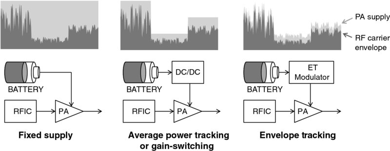
Figure 14.27 PA power supply control schemes
Gain-switching strategy relies on several PA gain modes, with each optimized for different output power ranges. Gain-switched PAs can be operated in either two or three modes. For example, a low power mode may be used from −50 dBm to around +6 dBm, a mid-power mode from +6 to around +16 dBm, and a high power mode for powers above +16 dBm. Each mode may be optimized separately to deliver the best compromise between spectral emissions and high efficiency. Since HSPA terminals spend most of their time transmitting at 0 dBm or below during voice calls, the low power mode of operation is one of the keys to delivering maximal battery life. In this mode, one common strategy consists of using RF switches to bypass an amplifier stage. Alternatively, PAs may use a dedicated secondary stage optimized for low current consumption. The benefits of toggling PA gain at a level of +17 dBm over a fixed power supply linear PA are illustrated in Figure 14.28 (diamonds vs. triangles). The relative savings remain advantageous even at low output powers. For example, at 17 dBm gain switching saves 40% current consumption (70 mA vs. 120 mA), while at 0 dBm battery current is reduced by 33% (14 mA vs. 21 mA). However, this technique presents several challenges: the toggling point must be selected carefully to ensure sufficient spectral emission margins to account for fabrication process spread, temperature, frequency, and battery voltage variations. Additionally, mode toggling in most cases generates a sudden gain and phase jump. Both impairments are bounded by specific 3GPP test cases. Each gain step must be calibrated in mass production and compensated by the UE transmitter chain to meet the TPC accuracy of ± 0.5 dB. Phase jumps must not exceed the phase discontinuity requirements [33] and may be digitally corrected by application of I/Q constellation rotation. If the phase jump is below 60 degrees, another simple technique consists in using separate threshold points for up and down power control commands. The toggling points are separated by at least 6 dB, effectively resulting in a hysteresis scheme which provides compliance to 3GPP requirements.
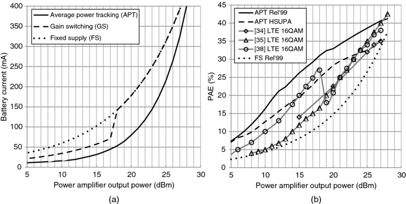
Figure 14.28 (a): APT, GS, FS PA battery current consumption for WCDMA rel'99 uplink transmissions. (b): Comparison of APT, FS, and ET power added efficiencies vs. output power. ET curves extracted from [34,35,38]
Average Power Tracking (APT) is a technique in which either the PA supply is adjusted, or both supply and bias voltages are altered, according to the amplifier output power level. In this scheme, a DC–DC converter decreases the supply voltage as the UE output power decreases. APT can be seen as an extension of the GS strategy, where adjustments are made on a slot-by-slot basis to deliver the best performance tradeoff over the mid- to high-output power range. Implementing APT in an open-loop (OL) fashion delivers the best cost and simplicity of implementation, but calls for mass production calibration of gain steps associated to each bias and supply setting. This technique may also be implemented in a closed-loop (CL) fashion, wherein the PA RMS output power is measured, digitally sampled, and compared to the targeted TX power. This algorithm may apply one, or several, fine gain corrections during the first few microseconds of a timeslot to ensure the target value is met within 3GPP accuracy requirements. Early implementations of this approach can be traced back to the first few generations of UEs (cf. Figure 14.5a, b and c), where the loop uses an RF directional coupler, a logarithmic RF power detector, a low-pass filter, and auxiliary ADC [4]. Modern CL implementations may replace the discrete power detector with a dedicated measurement receiver embedded within the RF TRX. For low power levels, the loop may be disabled, leaving the PA to operate OL in its low power mode. The main challenge in CL APT consists of ensuring that repetitive gain corrections do not impair the carrier's modulation properties. One example of this is the case of HS-DPCCH burst transmissions which are not time-aligned to the slot boundaries of other uplink physical channels. Also, power detector linearity must be excellent across a wide range of environmental conditions. Yet, as of today, APT remains the most efficient technique. Figure 14.28a shows an example of current consumption savings with APT (crosses). At 0 dBm, the savings are around 60% vs. a fixed supply. Even at high power levels the current consumption is slightly decreased because some amplifiers may be able to operate at 3.2 V, which is a lower voltage than the nominal battery voltage of 3.8 V.
Finally, a third technique called Envelope Tracking (ET) has recently received much attention. The concept, illustrated in Figure 14.27, consists in applying the smallest needed supply voltage in real-time, following the instantaneous envelope of the RF carrier. This may be seen as a real-time extension of APT. The current consumption gains are expected to be higher than with APT because the supply voltage is continuously adjusted to its lowest possible level without compromising the spectral emissions requirements. Interestingly, it enables better savings for high Peak-to-Average Power Ratio (PAPR) modulations, whereas APT efficiency decreases as PAPR increases because it requires a higher supply voltage to avoid PA clipping of the envelope peaks. For example, Figure 14.28b shows that the impressive level of performance achieved by the APT scheme for WCDMA rel'99 transmissions where the peak-to-average power ratio is typically 3 dB (at 0.1% probability of presence) and is noticeably degraded as soon as HSUPA transmissions occur (dashed-lines, cubic metric = 2). In this case, ET PAE exceeds that of HSUPA APT in the upper 6 to 7 dB output range.
However, ET implementation requires high-performance, high-speed DC–DC converter cores that are able to track the envelope of high bandwidth modulated carriers, such as LTE. The envelope being roughly the square of the IQ waveform, the bandwidth over which the DC–DC converter must deliver high efficiency becomes quite large. For instance, the envelope of a 20 MHz LTE carrier occupies 40 MHz. Delivering high supply modulator efficiencies over a large bandwidth and a large range of output powers is the key to ET exceeding APT performance. ET also requires tight time synchronization between the PA supply control path and the transceiver data IQ-to-RF path. Furthermore, high-speed supply modulators can degrade out-of-band noise emissions [37].
In both APT and ET, the total system efficiency is the product of PA and DC–DC converter efficiencies. In comparison to APT, the higher PA efficiency of ET is counter-balanced by a poorer DC–DC efficiency. It is easier to achieve high converter efficiency with APT than with ET, especially when ET is applied to a 20 MHz or greater modulation BW. Typically APT DC–DC converter efficiency can reach 90%, as opposed to the 70–80% range typical for ET [38]. Some solutions use a dual-supply modulator architecture resulting in an overall performance profile similar to that of GS (Figure 14.28 [38]). At the time of writing, it is difficult to assess the exact gains of ET, since only a couple of terminals have enabled this feature. Generally, current consumption gains are expected for the highest 6 dB output power levels. Considering that ET is still in its infancy, and that great progress has been made in only a couple of years (Figure 14.28 [34,35, 38]), there are good reasons to believe that ET will exceed APT performance levels. Since ET modulators may be entirely implemented in CMOS, this technology paves the way for commercial production of integrated linear CMOS PAs, provided that the cost of such products becomes attractive.
14.2.4 Continuous Packet Connectivity
CPC DRX / DTX is the most efficient technique to achieve significant power consumption savings as the UE entire cellular subsystem can be gated “On and Off.” Under ideal conditions [4], the power consumption can be in theory halved. Yet, in most cases, the end user perception is dominated by screen-related activity power consumption which remains constant during CPC operation. For example, halving the consumption in the HSPA background use case of Figure 14.22 reduces the UE power consumption by approximately 14%, a figure close to that reported in Chapter 13. This section describes some implementation aspects of DRX with a focus on the cellular subsystem.
CPC operation is complex to analyze. The first challenge consists in deriving the UE “On/Off” activity ratio which depends on a complex timing relationship between the various uplink and downlink physical channels. An illustration of this timing complexity can be found in [4] chapter 20 (section 20.4.5), a typical list of configuration parameters in chapter 4, table 1. To simplify the UE behavior, this section uses experimental measurement plots performed in LTE DRX connected mode with no or very little TX activity. This simplifies the examination of the UE “ON” time with respect to the eNodeB DRX cycle “on” duration. This section does not pretend to present an exhaustive list of events simply because DRX operation is optimized and fine tuned for a given chip set architecture. A detailed analysis would therefore reflect choices tailored to a specific vendor implementation.
DRX is often considered as a simple ON/OFF gating with instantaneous UE wake-up “twup” (or rise time) and power down “tpd” (or fall) transition times. In reality, it takes several milliseconds for the UE to transition from its deep sleep (DS) state to the active state and back again to DS. As a consequence, the real UE power consumption profile is better modelled as that of a wake-up, active “on” time “ton” and a power down profile as shown in Figure 14.29a. If the DRX cycle is too short, the UE may not be able to enter the DS state. In this case, the UE maintains a certain number of HW blocks and SW tasks active to deliver the best compromise between power consumption and system performance. The power consumption reaches a level that may be called “light sleep” (LS) as the power drained is somewhat at a level between the active and the DS state. Power consumption traces shown in Figure 14.29b have been measured on one recent triple mode UE and illustrate all above mentioned states and transitions. The minimum DRX cycle to enable DS on this UE is 64 ms. This phone would enter LS state for DRX cycle length between 64 and 32 ms, and would then stay at nominal power consumption for DRX cycle duration less than 32 ms. Assuming a similar wake-up/sleep processing time in WCDMA, this means that in numerous CPC configurations where the On/Off gap is only a few timeslot long, the UE cannot be gated to its complete “off” or DS state.
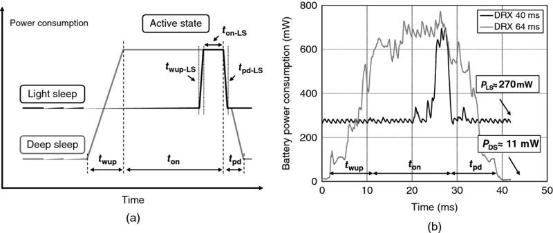
Figure 14.29 (a): UE power consumption model. (b): Power consumption traces measured on a recent Android based smartphone, in LTE DRX connected mode (no data transfer, no CQI transmission), in band 4. DRX cycle length 40 ms (black) is too short and UE remains in light-sleep state, with DRX 64 ms (gray) UE enters deep sleep state. eNodeB DRX “on” duration is set to 1 ms
14.2.4.1 Deep Sleep State
This state is similar to that achieved in standby/idle cell state. The UE runs off a low power, low frequency clock. Most UEs rely on a low cost 32.768 kHz crystal to maintain the minimum required number of HW blocks active. This state allows timers such as real-time clock and system frame number (SFN) to be updated at the lowest possible power consumption. In low-cost solutions, a tradeoff is often found between crystal oscillator cost/power consumption and oscillator jitter performance. A high 32 kHz jitter may require the UE to remain in DS state for a time long enough to ensure accurate SFN tracking. This prevents the UE from entering DS for certain DRX cycle lengths. In DS state, the entire RF subsystem is switched off, the BB modem is partially supplied, but no SW code is executed. A limited number of low-drop out (LDO) and DC–DC converters are activated. All power supply regulators dedicated to peripherals are switched off whenever possible (GPS, SD card, USB bus, etc.). Figure 14.30a shows that continuous efforts are made to improve the deep sleep state power consumption: the performance has improved by a factor of 2 across three generations of chip set. Controlling leakage current is key to delivering best in class performance in this state. One common strategy in SoC devices relies on hierarchical power domain distribution schemes as a complement to a clock distribution tree [39,40].
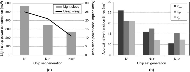
Figure 14.30 (a): Light (gray bars) and deep (black line) state power consumption vs. chipset generation. (b): State transition time evolution vs. chip set generations when UE transitions from DS to active state
14.2.4.2 Light Sleep State
The cellular subsystem runs off a low phase noise reference clock, which, depending on chip set vendors, is either a 26 MHz or a 19.2 MHz crystal. Most of the BB modem LDOs and DC–DC converters are active and the modem executes SW code. In most implementations, the RF subsystem is switched off. Architectures which rely on “smart RF transceivers” may maintain the TRX digital core active. The LS power consumption follows the general trends in reducing the active state power consumption optimization across generations of platforms [41]. Figure 14.30a shows power consumption has nearly improved by a factor of 2 over three generations.
14.2.4.3 DS to Active State Transition (wake-up “twup”)
This transition is a complex cascade of HW and SW events to progressively bring all HW blocks to the active state, in the fastest (shortest rise time) and most power efficient way. Power supplies rails, or power domains, are usually activated in a hierarchical scheme [39]. When a large number of gates must be activated, the sequential power-up technique helps prevent current rush/surge issues [40] from occurring. Due to battery internal resistance, these surges may generate a drop in battery voltage which at low operating voltages could, for example, trigger a UE shutdown sequence if detected by the power management unit. The sequential power-up delay between successive domains depends on the nature of the activity of the block being supplied. Delays range from 50–100 μs for digital PLL, 80–150 μs for RF LO PLL synthesizers, to 500 μs DC–DC converter typical settling time, to 2 ms required to stabilize the low phase noise reference clock oscillator (26 or 19.2 MHz). As soon as HW blocks are supplied, numerous activities can be parallelized to minimize wake-up time (twup). The near factor of 2 reduction of twup achieved across three generations of triple mode UEs shown in Figure 14.30b shows that despite the complexity of the task, chip sets are able to continuously improve performance.
14.2.4.4 Active State (“ton”) – Transition from DS
Several SW and HW tasks must be executed to prepare the subsystem for physical channel demodulation/modulation. From a SW perspective, resuming the SW context requires fetching data in LP-DDR to fill up the processor local cache memory. Depending on the operating system, and modem protocol stack complexity, this task can take several milliseconds. From an RF subsystem point of view, multiple initialization tasks must be executed. Preparing the receiver chain includes but is not limited to the following steps:
- Receiver self calibration (VCOs, channel filters).
- Switch on local oscillator and tune RF PLL frequency.
- Configure RX chain transceiver filters.
- Set antenna switch to selected band of operation.
- Switching on LNA and mixer.
- Prepare AGC algorithm: initial fast gain acquisition or tracking mode?
- Set the initial RX chain gain (LNA, mixer, I/Q analog VGAs).
- Switch on I/Q ADC (in RF transceiver if digital IQ interface, in modem BB otherwise).
Once the RF IC is ready, a critical algorithm to deliver a power efficient performance is that of fast gain control, also sometimes referred to as fast gain acquisition (FGA). In WCDMA, this should ideally be completed within less than one timeslot (666.66 μs). FGA is common to compressed mode and DRX operation. Its goal is to ensure the I/Q ADC is operated at its optimal back-off. Because of multipath fading, a compromise must be found between RRSS (receiver radio signal strength) integration period to ensure good Ior power measurement accuracy, the number of gain corrections, gain step size boundaries, and initial gain settings to ensure convergence to the target ADC back-off across the entire UE dynamic range in a minimum number of steps. Most chip sets manage to achieve this task using three gain adjustments. One of the challenges with FGA is that ZIF receiver self-mixing due to uplink carrier leakage generates a time varying DC offset which, if not cancelled, could lead to erroneous Ior power measurements. DC offset compensation in WCDMA is often achieved via an equivalent high-pass filtering function, either in analog IQ, digital IQ, or a combination of coarse analog IQ and fine digital IQ DC offset compensation. The higher the equivalent HPF cut-off frequency, the higher the EVM. Since, during FGA, only RRSS measurement accuracy matters (i.e., EVM is not a concern), fast DC settling time can be achieved by selecting a high cut-off frequency. Once FGA is completed, the DC offset compensation circuitry must resume its low EVM, low cut-off frequency. The target ADC back-off can then be locked through a standard AGC loop. Finally, the UE must perform RF channel estimation. With the introduction of recent high-speed train fading profiles, the UE may have to adapt its channel estimation averaging time and update rate based on an estimation of its velocity. At high speed, a longer and more frequent channel estimation might be required. These are some of the key tasks the system must complete prior to demodulation.
14.2.4.5 LS to Active State Transition (“ton-LS”)
In most UEs, this task consists in activating the RF subsystem as the entire modem and SW code is active. The delays associated with this task are those of the previously listed sequence. The active time which follows a transition from LS state (“ton-LS”) should in theory be shorter since the only tasks required are: program default gain, and frequency values, perform FGA, and channel estimation. In the example of Figure 14.29b, twup-LS lasts less than 1 ms and ton-LS is approximately equal to 2.6 ms for an eNodeB DRX cycle “on duration” of 1 ms.
14.2.4.6 Active State to LS to DS Transition
Switching off the RF subsystem is more straightforward and faster than the activation procedure. All blocks can be switched off nearly instantaneously. The remaining power-down delays are SW stack-related.
Finally, Figure 14.31 shows the CPC battery savings that are achieved in practice on a recent triple-mode UE operating in band 4. The measurements are performed using an Anritsu 8475a NodeB emulator during an FTP download sequence restricting the UE to operate in single cell mode, HSDPA cat 14, HSUPA cat 6. CPC parameters are similar to those of Chapter 4, Table 4.1. It can be seen that despite large inactive gaps, the UE power consumption profile is far from reaching the ideal DS power consumption. In this case, the UE power consumption savings are 18% with screen “off,” and 7% when the screen is activated. The average downlink MAC layer throughput is approximately 12 Mbit/s.
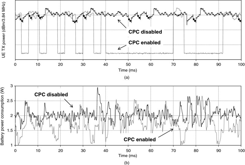
Figure 14.31 CPC battery consumption savings and UE TX power gating vs. time during an FTP file download in HSDPA cat 14. (a): UE TX power with CPC enabled vs. CPC disabled. (b): UE battery power consumption with screen “switched OFF”
Figure 14.32 has been captured by stalling the FTP download process so as to minimize the impact of background FTP server application SW tasks onto the cellular subsystem power consumption. The UE remains in CPC DTX DRX connected mode, with very few packets to receive (near zero downlink throughput), or transmit. The graph shows the UE power consumption profile closely matching the UE TX power mask when CPC is activated. The power consumption bumps between two transmissions are likely related to DRX activity. The screen is “off” but the FTP server application is still running in the background. The UE power consumption savings are close to 51%.
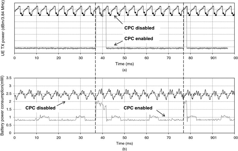
Figure 14.32 CPC battery consumption savings and UE TX power gating vs. time during a stalled FTP file download session. (a): UE TX power with CPC enabled vs. CPC disabled. (b): UE battery power consumption with screen “switched OFF”
14.3 Conclusion
The key to successful designs in the mobile terminal industry has always been, and still remains, to deliver a timely solution that meets the desired price/performance/power consumption tradeoffs. However, it is important to note that the proper balance of these criteria is a goal that remains constantly in flux, due to the ever-changing demands and expectations of the consumer. With the wide adoption of smartphones, this tradeoff becomes ever more difficult, as the number of use cases has increased considerably. From an application engine standpoint the terminal must support a wide range of additional performance requirements, from the lower demands of texting/chatting applications, to the highly demanding 3D gaming, satellite navigation, augmented reality, or even video editing applications. The always-on requirement combined with the need to minimize product variants force transceiver designers to produce solutions that must be able to support as many of the 40 standardized frequency bands (29 FDD-LTE, 12 TD-LTE) as is possible. This, in turn, requires a multiplicity of implementation improvements, including antennae to deliver optimal efficiency across a wide range of frequency bands. From a power consumption point of view, and despite the availability of moderately higher capacity batteries, designers must deliver solutions that ensure at least a full day of use under these demanding usage conditions. In this context, the traditional design challenges of earlier generations of terminals are exacerbated as a consequence of the increasing device complexity and increased consumer expectations. Some of the resultant outcomes of this new usage paradigm for terminal designers include:
- OTA performance will have a major impact on MIMO user experience.
- Cellular transceivers must be able to support a continuously increasing number of bands, as well as the complex band combinations to support carrier-aggregation.
- As a consequence, co-existence scenarios are becoming more complicated to resolve as the number of radio-to-radio, as well as the number of digital-to-radio subsystems operating simultaneously increases.
- The limited thermal envelope of the device places severe constraints on how to best deliver expected user experience across a wide range of use cases in a small form factor.
Admittedly these challenges present opportunities for innovation, and the industry has a history of embracing challenges, so there is reason to believe it will do so again and thus will find innovative means to effectively solve these issues. This short introduction to this topic has attempted to highlight that one of the keys to delivering successful solutions has become to rely more heavily upon reconfigurable hardware architectures in as many blocks and functions as possible, such as:
- Use of hybrid CPUs in the application engine.
- Extensive use of digital signal processing in the RF transceiver, thanks to the availability of low power, high dynamic range ADCs and DACs, making the transceiver easily reconfigurable to support multiple air interfaces.
- Tunable antennae to optimize performance across a wide range of operating frequencies.
- Multimode, multiband power amplifiers.
The RF front end remains an area which still possesses less-than-optimal reconfigurability. Since today high performance dedicated RF filters and RF multiplexers are required per band or for selected band combinations, this makes the cellular RF-FE one of the primary areas where substantial challenges lie ahead for next-generation platforms. And looking ahead to carrier-aggregation, the RF front end will become even more complex, so there is a need to achieve greater reuse and reconfigurability in all areas.
Market segmentation does not help in this respect either, as platforms must be optimized for each market segment. A recent forecast indicates that low-end smartphones (<$200 price), and, to a certain extent mid-range devices ($200–300 retail price), are expected to dominate market growth, with 3x and 50% increase, respectively, by 2018. Therefore, most of the design tradeoffs which have been mentioned in this chapter must be re-assessed for each market segment and appropriate changes must be made. This increases the R&D work load for terminal designs – all in an industry where meeting an aggressive time-to-market is a primary key to success. The combination of all these constraints, as well as the pressure of huge production volumes, probably qualifies the design of the modern mobile terminal as one of the most challenging design environments in the electronics industry.
To put this in perspective – how many terminal devices or chip sets will have been shipped throughout the world by the time you read this sentence?
Notes
References
- Gartner press release (April 4, 2013), “Gartner Says Worldwide PC, Tablet and Mobile Phone Combined Shipments to Reach 2.4 Billion Units in 2013”, http://www.gartner.com/newsroom/id/2408515 (last checked August 2013).
- R2-124396, “LS on extending E-UTRA band number and EARFCN numbering space”, 3GPP TSG RAN WG2 Meeting #79bis, Bratislava, Slovakia, 8–12 October 2012.
- Graph compiled using data extracted off a total of 125 mobile phone teardown reports, mostly licensed from UBM Techinsights (www.ubmtechinsights.com) and partially from ABI research (http://www.abiresearch.com). Breakdown: 69 monomode EGPRS teardown reports, 48 dual-mode EGPRS-WCDMA terminals, 7 triple-mode EGPRS-WCDMA-LTE terminals.
- Holma, H. and Toskala, A. (2010) WCDMA for UMTS: HSPA Evolution and LTE, 5th edn, chapter 20, John Wiley & Sons, Ltd, Chichester.
- Holma, H. and Toskala, A. (2011) LTE for UMTS: Evolution to LTE-Advanced, 2nd edn, John Wiley & Sons, Ltd, Chichester.
- Jones, C., Tenbroek, B., Fowers, P. et al. (2007) Direct-Conversion WCDMA Transmitter with −163 dBc/Hz Noise at 190 MHz Offset. Solid-State Circuits Conference, 2007. ISSCC 2007. Digest of Technical Papers. IEEE International, pp. 336–607.
- Kihara, T., Sano, T., Mizokami, M. et al. (2012) A multiband LTE SAW-less CMOS transmitter with source-follower-drived passive mixers, envelope-tracked RF-PGAs, and Marchand baluns. Radio Frequency Integrated Circuits Symposium (RFIC), IEEE, pp. 399–402.
- Xie, H., Oliaei, O., Rakers, P. et al. (2012) Single-chip multiband EGPRS and SAW-less LTE WCDMA CMOS receiver with diversity. IEEE Transactions on Microwave Theory and Techniques, 60(5), 1390–1396.
- Gaborieau, O., Mattisson, S., Klemmer, N. et al. (2009) A SAW-less multiband WEDGE receiver. Solid-State Circuits Conference – Digest of Technical Papers, 2009. ISSCC 2009. IEEE International, pp. 114–115, 115a.
- Intel XMM6140 dual-mode EGPRS-HSDPA single-chip modem, power management unit, RF transceiver solution, http://www.intel.com/content/www/us/en/wireless-products/mobile-communications/mobile-phone-platforms.html.
- Broadcom BCM21892, “4G LTE Advanced FDD and TDD; 3G HSPA +and TD-SCDMA; 2G-EDGE Modem with Integrated World-Band Radio”, February 2013, http://www.broadcom.com/products/Cellular/4G-Baseband-Processors/BCM21892.
- R4-121361, “LO coupling issues for NC intra-band CA”, 3GPP TSG-RAN WG4 Meeting #62bis, Jeju Island, Korea, 26–30 March, 2012.
- R4-131235, “Considerations for single-chip implementations of carrier aggregation”, 3GPP TSG-RAN WG4 Meeting #66 Bis, Chicago, U.S.A, 15th April – 19th April, 2013.
- Abdelhalem, S.H., Gudem, P.S. and Larson, L.E. (2012) A tuneable differential duplexer in 90nm CMOS. Radio Frequency Integrated Circuits Symposium (RFIC), 2012 IEEE, pp. 101–104.
- Sony Mobile C6903 (PM-0450-BV), supported bands LTE: 1,2,3,4,5,7,8,20; HSPA+/UMTS:I,II,IV,V,VIII; GSM-GPRS-EDGE:850/900/1800/1900 MHz http://www.gsmarena.com/sony_xperia_z_ultra-5540.php (last checked Aug. 2013).
- R4-133985, ‘On the additional insertion-loss for CA_2A-4A’, TSG-RAN Working Group 4 (Radio) meeting #68, Barcelona, Spain, 19–23 August 2013.
- 2012 CES Innovations Design and Engineering Awards in category ‘Embedded Technologies’: Renesas SP2531 (Pegastick) triple mode (EDGE,HSPA+,LTE) USB datacard, http://www.cesweb.org/cesweb/media/CESWeb/ Innovation%20Awards/2012%20Innovations%20Honorees/Embedded%20Technologies/Pegastick.bmp.
- “Test Plan for Mobile Station Over the Air Performance, Method of Measurement for Radiated RF Power and Receiver Performance”, revision 3.2.1, CTIA – The Wireless Association®, March 2013.
- Pelosi, M., Franek, O., Knudsen, M.B. et al. (2010) Antenna Proximity Effects for Talk and Data Modes in Mobile Phones. Antennas and Propagation Magazine, IEEE, pp. 15–27.
- Ranta, T., Ella, J. and Pohjonen, H. (2005) Antenna switch linearity requirements for GSM/WCDMA mobile phone front-ends. The European Conference on Wireless Technology 2005, pp. 23–26.
- Del Barrio, S.C. and Pedersen, G.F. (2012) Correlation Evaluation on Small LTE Handsets. Vehicular Technology Conference (VTC Fall), 2012 IEEE, Quebec City, pp. 1–4.
- Yanakiev, B., Nielsen, J.O., Christensen, M. and Pedersen, G.F. (2012) On Small Terminal Antenna Correlation and Impact on MIMO Channel Capacity. IEEE Transactions on Antennas and Propagation, 689–699.
- R4-66AH-0003, “Effect of user-presence on MIMO OTA using an anechoic chamber and a reverberation chamber”, TSG-RAN Working Group 4 (Radio) Meeting #66 Ad hoc, Munich, Germany, 12–13 March, 2013.
- Boyle, K. and Leitner, M. (2011) Mobile phone antenna impedance variations with real users and phantoms. International Workshop on Antenna Technology (iWAT), 2011, pp. 420–423.
- Wu, T.-H., Chang, H.-H., Chen, S.-F. et al. (2013) A 65-nm GSM/GPRS/EDGE SoC with integrated BT/FM. IEEE Journal of Solid-State Circuits, 48(5), 1161–1173.
- R4-124113, “REFSENS analysis using MSD methodology for Band 4 and Band 17 carrier aggregation”, 3GPP TSG RAN WG4 Meeting #64, Qingdao, China, Aug., 13th – 17th, 2012.
- R4-121862, “Cross-coupling of Harmonics in case of band 17/4 Carrier Aggregation”, 3GPP TSG-RAN WG4 Meeting #62bis, Jeju, Korea, March 26 – 30, 2012.
- R4-124359, “Interband CA Class A2 MSD”, TSG-RAN Working Group 4 (Radio) meeting #64 Qingdao, P.R.China, Aug 13th – 17th, 2012.
- Experian marketing (May 2013), John Fetto, “Americans spend 58 minutes a day on their smartphones”, http://www.experian.com/blogs/marketing-forward/2013/05/28/americans-spend-58-minutes-a-day-on-their-s martphones/ (last accessed August 2013).
- Cameron, K.W. and Ge, R. (2012) Generalizing Amdahl's law for power and energy. IEEE Computer, 45(3).
- Rasmussen, M. (2013) Using Task Load Tracking to Improve Kernel Scheduler Load Balancing. The Linux Foundation Collaboration Summit, Apr 15–17 2013.
- NEC Casio X medias N-06E product launched by NTTdocomo in July 2013, http://www1.medias.net/jp/sp/n06e, and http://www.gsmarena.com/nec_medias_x_has_a_watercooled_snapdragon_s4_pro_chipset-news-6043.php.
- 3GPP TS 25.101 V12.0.0 (2013-07), www.3gpp.org.
- Honda, Y., Yokota, Y., Goto, N. et al. (2012) A wide supply voltage and low-rx noise envelope tracking supply modulator IC for LTE handset power amplifiers. 2012 42nd European Microwave Conference (EuMC), 2012, pp. 1253–1256.
- Kim, D., Kang, D. and Jooseung, K. (2012) Wideband envelope tracking power amplifier for LTE application. Radio Frequency Integrated Circuits Symposium (RFIC), 2012 IEEE, pp. 275–278.
- Kaczman, D.L., Shah, M., Godambe, N. et al. (2006) A single-chip tri-band (2100, 1900, 850/800 MHz) WCDMA/HSDPA cellular transceiver. IEEE Journal of Solid-State Circuits, 41(5), 1122–1132. Noise at 12.5 MHz offset is the only value published.
- R4-132882, “Envelope tracking measurement results”, 3GPP TSG RAN WG4 #67, 20 –24 May 2013, Fukuoka, Japan.
- Kim, J., Dongsu, K., Yunsung, C. et al. (2013) Envelope-tracking two-stage power amplifier with dual-mode supply modulator for LTE applications. IEEE Transactions on Microwave Theory and Techniques, 61, 543–552.
- Kim, G.S., Je, Y.H. and Kim, S. (2009) An adjustable power management for optimal power saving in LTE terminal baseband modem. IEEE Transactions on Consumer Electronics, 55(4), 1847–1853.
- Kanno, Y., Mizuno, H., Yasu, Y. et al. (2007) Hierarchical power distribution with power tree in dozens of power domains for 90-nm low-power multi-CPU SoCs. IEEE Journal of Solid-State Circuits, 42(1), 74–83.
- Lauridsen, M., Noël, L. and Mogensen, P.E. (2013) Empirical LTE Smartphone Power Model with DRX Operation for System Level Simulations. Vehicular Technology Conference (VTC Fall), 2013 IEEE.
- R4-120442, Way forward for inter-band CA Class A2. 3GPP TSG-RAN WG4 Meeting #62, Dresden, Germany, Feb 6th – 10th, 2012.
- Tomiyama, H., Nishi, C., Ozawa, N. et al. (2006) Low voltage (1.8 V) operation triple band WCDMA transceiver IC. Radio Frequency Integrated Circuits (RFIC) Symposium, 2006.
- Koller, R., Ruhlicke, T., Pimingsdorfer, D. and Adler, B. (2006) A single-chip 0.13 /spl mu/m CMOS UMTS W-CDMA multi-band transceiver. Radio Frequency Integrated Circuits (RFIC) Symposium, 2006.
- Jones, C., Tenbroek, B., Fowers, P. et al. (2007) Direct-Conversion WCDMA Transmitter with −163 dBc/Hz Noise at 190 MHz Offset. Solid-State Circuits Conference, 2007.
- Sowlati, T., Agarwal, B., Cho, J. et al. (2009) Single-chip multiband WCDMA/HSDPA/HSUPA/EGPRS transceiver with diversity receiver and 3G DigRF interface without SAW filters in transmitter / 3G receiver paths. Solid-State Circuits Conference, 2009, pp. 116–117, 117a.
- Huang, Q., Rogin, J., XinHua, C. et al. (2010) A tri-band SAW-less WCDMA/HSPA RF CMOS transceiver with on-chip DC-DC converter connectable to battery. Conference Digest of Solid-State Circuits (ISSCC), 2010, pp. 60–61.
- Tsukizawa, T., Nakamura, M., Do, G. et al. (2010) ISO-less, SAW-less open-loop polar modulation transceiver for 3G/GSM/EDGE multi-mode/multi-band handset. Microwave Symposium Digest (MTT), 2010 IEEE, pp. 252–255. Transceiver.
- Hausmann, K., Ganger, J., Kirschenmann, M. et al. (2010) A SAW-less CMOS TX for EGPRS and WCDMA. Radio Frequency Integrated Circuit Symposium (RFIC), 2010, pp. 25–28.
- Giannini, V., Ingels, M., Sano, T. et al. (2011) A multiband LTE SAW-less modulator with −160 dBc/Hz RX-band noise in 40 nm LP CMOS. Solid-State Circuits Conference Digest of Technical Papers (ISSCC), 2011 IEEE, pp. 374–376.
- Oliaei, O., Kirschenmann, M., Newman, D. et al. (2012) A Multiband Multimode Transmitter without Driver amplifier. Solid-State Circuits Conference Digest of Technical Papers (ISSCC), 2012 IEEE, pp. 164–166.
- ABI Research, ‘Sub-$200 Smartphone Shipments to Exceed 750 Million in 2018’, Oyster Bay, New York – 07 Aug 2013 press release, http://www.abiresearch.com/press/sub-200-smartphone-shipments-to-exceed-750-million.
- Apple A1475 supports a total of 22 bands. LTE Band 1, 2, 3, 4, 5, 7, 8, 13, 17, 18, 19, 20, 25; HSPA+/UMTS:I,II,IV,V,VIII; GSM-GPRS-EDGE:850/900/1800/1900 MHz.