CHAPTER 7
![]()
Bipolar Junction Transistors
In previous chapters, we have dealt with two terminal electronic components such as resistors, capacitors, diodes, and LEDs. We will now explore the commonly used bipolar junction transistors (BJTs, also known as bipolar transistors), which are three-terminal devices. They are in many do-it-yourself (DIY) projects and manufactured products.
Bipolar Junction Transistors
The first transistor was invented at Bell Laboratories in 1948. It had a point contact type of construction that was difficult to manufacture. The point contact transistor technology was replaced by the (alloy) junction transistor that was more easily manufactured. Alloy junction germanium transistors such as the CK722, 2N107, 2N109, 2N408, 2SB32, 2SB54, 2SB56, 2SB75, 2SB77, 2SB113, 2SB115, AC125, AC126, OC71, and OC72 were quite prevalent from the mid-1950s to the late 1960s.
So, what is a transistor? The bipolar transistor is a three-terminal device that allows controlling large amounts of output current by a small change in input current or voltage. Thus, a bipolar transistor can be used as an amplifier where a small input signal can provide a larger signal at its output, with the “help” of a power supply. That is, transistors by themselves cannot amplify or control large electrical current unless there is a supply voltage included in the transistor circuit.
The three terminals to a bipolar transistor are:
• The emitter as identified by the letter “E” or “e”
• The base as identified by the letter “B” or “b”
• The collector as identified by the letter “C” or “c”
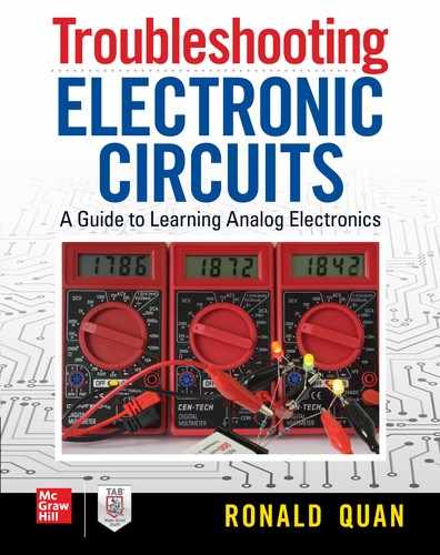
See Figure 7-1 for bipolar transistors with different plastic packages. These range from small signal transistors (TO-92) to power transistors (TO-220 and TO-247).
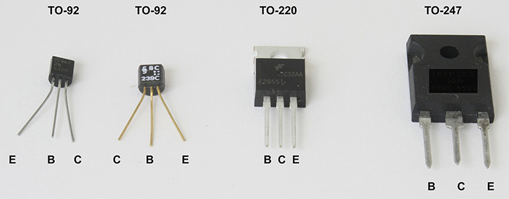
FIGURE 7.1 Various transistors. Note the different pin outs for the two TO-92 transistors.
Most plastic small-signal transistors (e.g., < 500 mA collector current) with 2N or PN prefixes, such as 2N3904, 2N4124, 2N4401, PN2222 or 2N5089, have the pin out sequence E, B, C as shown in the first transistor on the left in Figure 7-1. This left-to-right emitter, base, collector sequence is taken as you look at the transistor with the flat side up.
In Europe, transistors that generally have a prefix of BC, such as BC548, BC556, or BC239C (as shown in Figure 7-1, second transistor from the left side), and other part numbers with a P2N prefix, such as P2N2222A and P2N2907A, have a “reversed” pin out sequence of C, B, E. The left-to-right collector, base, emitter sequence is taken when you look at the transistor flat side up.
For the two power transistors shown in Figure 7-1, the sequence, taken left to right with the part number side up or facing you, is base, collector, emitter, or B, C, E. Note that the metal tab in the TO-220 transistor actually extends further down in the back of the transistor. This metal tab is connected to the middle lead or collector of the TO-220 power transistor. In general, with very few exceptions, it is very important to insulate or to ensure that the metal tab is not connected to ground or to some other point of a circuit. TO-220 transistors have maximum collector currents of about 10 amps. However, for many power applications such as driving loudspeakers or motors, the TO-220 transistor should be mounted on a heat sink with a thermally conductive insulated sheet or washer.
The TO-247 transistor in Figure 7-1 can handle collector currents greater than or equal to 15 amps. Not shown but in its back side is an exposed metal piece that is also connected to the middle lead or collector of the power transistor. Again, if the transistor is delivering high power (> 5 watts) to a load such as a motor, loudspeaker, or lamp assembly, a heat sink is required. The TO-247 transistor would be mounted on a heat sink via a thermally conductive insulated sheet or washer. See Figure 7-2 for various TO-220 heat sinks.
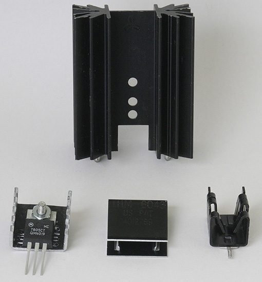
FIGURE 7.2 Various TO-220 heat sinks with an example TO-220 voltage regulator mounted on the bottom-left side.
Transistors also come in metal packages, and the two most common ones are TO-18 and TO-5 (see Figure 7-3). These transistors have protruding tabs, which identify the emitter terminals.
FIGURE 7.3 TO-5 transistors on the left and the smaller TO-18 transistors on the right.
In metal case transistors the middle lead will usually be the base terminal. To find the emitter lead, find the tab that is located next to it. The remaining lead opposite the emitter terminal is the collector. Another way is to look at the bottom of the metal case transistor with the middle lead pointing to “12 o’clock.” The emitter lead will be to the left of “9 o’clock,” and the collector lead will be on the right that is analogous to a “3 o’clock” position.
Generally, metal case small and medium collector current transistors are not used as much, and they have been replaced with plastic package transistors. One reason is cost, and another is that they only offer a little more collector current capability than some plastic case transistors of the similar sizes. What you will see, however, is that metal case transistors were used often in older equipment (e.g., older Hewlett Packard solid state signal generators, vintage stereo amplifiers, tuners, and receivers, or ham radio transceivers, transmitters, and receivers). So, it is good to know about metal case transistors when you are fixing or modifying older circuits.
It is very important to know the pin out for each transistor you use because none of the three terminals is interchangeable. For example, if you reverse the collector and emitter leads, your circuit will not work properly. In other cases, mis-wired transistor leads can result in damage.
In general, a damaged transistor usually has two characteristics:
1. Shorted collector to emitter junction, which when measured with an ohm meter, the normally “open” or infinite ohms reading goes to a low resistance reading of typically < 10Ω.
2. Open base to emitter junction, which means if you use your DVM’s diode voltage testing function, you do not get typically 0.6 volts to 0.7 volts, but instead get an “error” reading.
However, because most DVMs have a transistor tester, you can just test the transistor. For power transistors, you can solder wires to their terminals for easier testing in a DVM.
If you have never seen a transistor in a circuit and want to just test it, what would you look for? The DVM tests for current gain known as Hfe, hFE, beta, or the Greek letter beta, β. Generally, a good transistor will have a current gain of 10 or more.
Current gain is defined as the ratio of the collector current, IC, to the base current, IB. That is:
![]()
Or put in another way, IC = β IB.
Typically, 15 < β < 500.
For example, if we have 1 μA of base current, IB, and the β = 250, then the collector current:
IC = 250 × 1 μA
or
IC = 250 μA
Typically, small signal (TO-92) and metal case transistors (e.g., TO-5 and TO-18) have ≥ 20 current gain. If the transistor is mis-wired and connected backwards in terms of the collector and emitter terminals, then you will see a substantial current gain decrease to typical numbers of 0 < β < 4.
See Figures 7-4 and 7-5, which show testing a 2N2906 (TO-18) transistor.

FIGURE 7.4 A TO-18 transistor with its emitter tab pointed up toward “E” with the DVM selector knob set to hFE. Here, we see the transistor has a current gain, hFE = 78.
FIGURE 7.5 The same transistor tested “backwards” with the emitter inserted in the collector, C, portion of the socket and the transistor’s collector lead inserted into the E portion of the socket. Note that the tab that identifies the emitter is pointing down. The resulting current gain is very low at hFE = 1 when the transistor is wired backwards this way.
There are two types of bipolar transistors, NPN and PNP. To identify the transistor, you can plug the test transistor into the NPN socket and test, and then do the same in the PNP socket. Only one socket will give you a correct reading, which is usually a number between 15 and 1000. The other way to identify the transistor is to read the part number printed on the case and look up the data sheet. For example, the transistor being tested is a 2N2906, which its data sheet identifies as a PNP transistor.
Now, should you swap or reverse the collector and emitter leads, while having the base lead correct, you will find that the current gain is hFE = 1. See Figure 7-5.
What Happens When a Transistor Is Damaged
Transistors, just like diodes, share a couple of common specifications. One is the maximum voltage, and the other is the maximum current. When either of these specifications is exceeded, the transistor can be damaged. The typical blown or damaged transistor suffers from any combination of a short circuit or low resistance between the collector and emitter that can be verified with an ohm meter. Make sure to test the collector and emitter leads with the test leads one way and then the other—for example, the red test lead connected to the collector and black test connected to the emitter. Then switch the ohm meter’s leads where the black test lead is connected to the collector and the red test lead is connected to the emitter. Note the two resistance readings, which should be <20Ω if the transistor is damaged via a short from collector to emitter.
A damaged transistor can have an open circuit between the base and emitter terminals. This can be verified by using the DVM’s diode voltage test as shown in Figure 7-6.
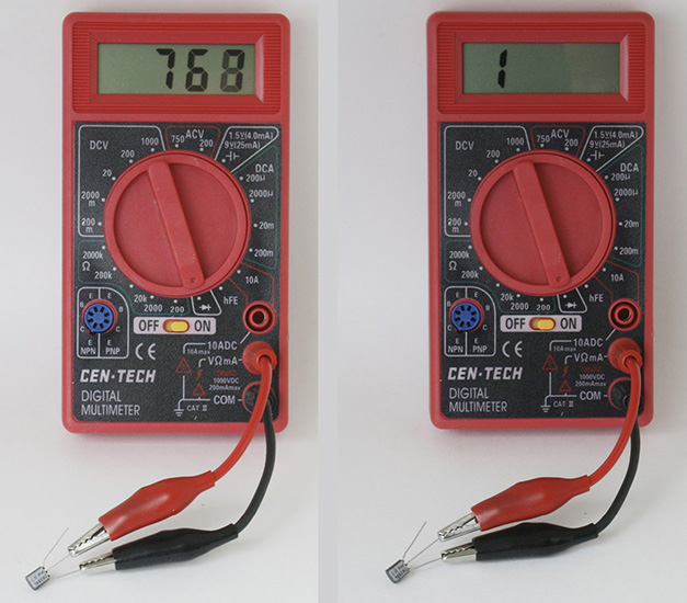
FIGURE 7.6 Testing the base-to-emitter voltage with the DVM where the one on the left is good with a forward base-to-emitter voltage reading of ~0.768 volt in three digits. But the one on the right is damaged with a single digit “1” that indicates an open circuit. If the reading is not in the 0.7-volt range, reverse the test leads just in case you are testing a transistor of the opposite polarity (e.g., NPN versus PNP, or PNP versus NPN). It is sometimes easy to incorrectly think of which type of transistor you are testing because of a misread transistor part number.
Schematic Symbol of NPN and PNP Transistors
In most circuit schematic diagrams, transistors are designated with a “Q” prefix such as Q1, Q2, Q3, etc. (See Figure 7-7.) Alternatively, sometimes the transistors are labeled with a prefix of “TR,” which results in TR1, TR2, TR3, etc., or sometimes with a dash in between like TR-1, TR-2, TR-3, and so on.

FIGURE 7.7 Schematic symbols for NPN (Q1) and PNP (Q2) with their terminal’s emitter, base, and collector labeled equivalently as E, B, and C.
NOTE: The arrows in the emitter terminals show the direction of positive current flow.
Applying a DC Voltage to the Base of the Transistor to Provide a Constant Current Source
To reiterate, the transistor is an electrical current controlling device. In most cases, it provides current gain and/or voltage gain from an input to an output. Let’s take a look at several circuits where the transistor works as a constant current source. In the first examples, a small base current, IB, at the “input” results in a large collector current, IC, at the “output.” See Figure 7-8.
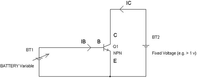
FIGURE 7.8 A constant current source via collector output current IC. A variable power supply voltage source, BT1, is applied directly to the base-emitter junction, which can damage the transistor Q1.
In Figure 7-8 a positive voltage, BT1, is applied to the base with respect to the emitter. And the output current, IC, requires a positive voltage to the collector with respect to the emitter.
A basic principle of biasing a transistor is shown in Figure 7-8, which is not normally done in practice because the transistor can be easily damaged this way. Biasing is a way of turning on the transistor Q1 via applying a bias voltage, BT1, across the base and emitter terminals. In this case variable voltage source BT1 is turned up to a voltage generally in the range of 0.6 volts to 0.7 volts to generate a collector current IC at the output. However, in practice this method is rarely used because if BT1 exceeds 0.8 volts, the transistor may burn out and either the collector and emitter terminals get shorted out due to excessive collector currents and/or the base-emitter junction becomes like an open circuit. This happens because the bipolar transistor has an exponential relationship between the base-emitter voltage and collector current. So, what does this really mean? It means that a small increase in base-emitter voltage (e.g., from BT1) will result in a large increase in collector current.
For example, if a transistor has 1 mA collector current for a BT1 set to 0.600 volt, the collector current will increase to 10 mA for BT1 = 0.660 volt, and 100 mA when BT1 = 0.720 volt. As you can see, every increase in 60 mV causes a change in collector current by 10-fold.
Another reason not to directly drive the base-emitter junction directly with a voltage source is that every transistor has slightly different turn-on voltage. Generally, a power transistor will have slightly lower turn-on voltage. But even transistors of the same type (e.g., small-signal) or same part number can have base-emitter turn-on voltages that are different by 60 mV or more due to the transistor manufacturing process. This means that without sorting or measuring each transistor, you can get a 10:1 variation in collector current for the same base-emitter bias voltage.
Just like LEDs, transistors have maximum base current and collector current ratings. Generally, we look for the maximum collector current specification that is found in a data sheet.
For example, a very popular general purpose NPN transistor, 2N3904 (TO-92 plastic case, see Figure 7-1), has a maximum collector current rating of about 200 mA. For higher currents, a popular NPN power transistor is the MJE3055T transistor (TO-220 case, see Figure 7-1) that has a 10-amp collector current rating.
In practical transistor circuits, generally the base and/or emitter will include a resistor to help “stabilize” the collector current, which allows for plugging in different transistors while providing essentially a reliable or known collector current. Figure 7-9 shows simple series base resistor biasing. This type of circuit was used often in the early days of transistor circuits back in the 1950s. It can still be used today but there are problems with this circuit because β can vary from one transistor to another, which means the collector current will vary for a given fixed base current.
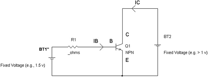
FIGURE 7.9 Biasing a transistor via a series base resistor, R1, to set a collector current IC.
To prevent accidental damage to the transistor due to excessive collector current, the series base resistor R1 isolates BT1 from connecting its voltage directly to the base-emitter terminals. The collector current IC then can be calculated in the following manner.
Again, we need to reiterate that current gain is the ratio of IC (collector current) to IB (base current), or:
![]()
There are two commonly used symbols for transistor current gain, β and hFE, which are one and the same. Thus:
![]()
With a little algebra, we can find the collector current if we know the current gain and base current. In this book β and hFE are interchangeable. Thus:
IC = β IB
For example, if β = hFE = 100 and IB = 10 μA, then IC = 100 × 10 μA or IC = 1000 μA = 1 mA.
In Figure 7-9, the base current, IB, is the current flowing through R1. We can determine the current flowing through R1 by finding the potential difference across R1.
IB = (BT1 – VBE)/R1
If we know the battery voltage BT1, and approximate that VBE is in a narrow range of 0.6 volt to 0.8 volt, we can use a value in the middle such as 0.7 volt for VBE. Thus, IB = (BT1 – 0.7 volt)/R1.
IC = β IB so:
IC = β (BT1 – 0.7 volt)/R1
For example, suppose R1 = 100KΩ and β = 100, with BT1 = 1.5 volts.
IC = 100 (1.5 volts – 0.7 volt)/100KΩ = 100 (0.8 volt)/ 100KΩ = 80 volts/100KΩ
IC = 0.0008 amp or 0.8 mA or 800 μA
If the β = 300, then IC = 300 (1.5 volts – 0.7 volt)/100KΩ = 0.0024 amp or 2.4 mA.
The current gain β or hFE is usually specified by the transistor’s data or specification sheet. Also, β or hFE normally has a wide range such as 3:1. For example, the β can vary from 50 to 150 for some transistors, and 100 to 300 for others.
NOTE: In Chapter 6 we stated that an LED is generally not to be driven directly with a voltage source such as a power supply. This applies the same to any base-emitter junction. A base-emitter junction directly driven with a low-resistance power supply can result in damaging the transistor. Often, when excessive current has been applied to the base, the base-emitter junction becomes an open circuit and thus no longer conducts or allows base current to flow. This open circuit between the base and emitter, due to damage, will usually result in zero collector current.
We will now show examples of biasing a transistor via a series base resistor. See Figures 7-10 and 7-11, which illustrate driving LEDs.
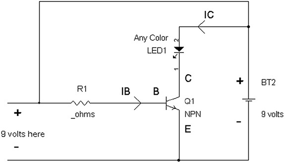
FIGURE 7.10 A simple LED driver circuit using an NPN transistor current source.
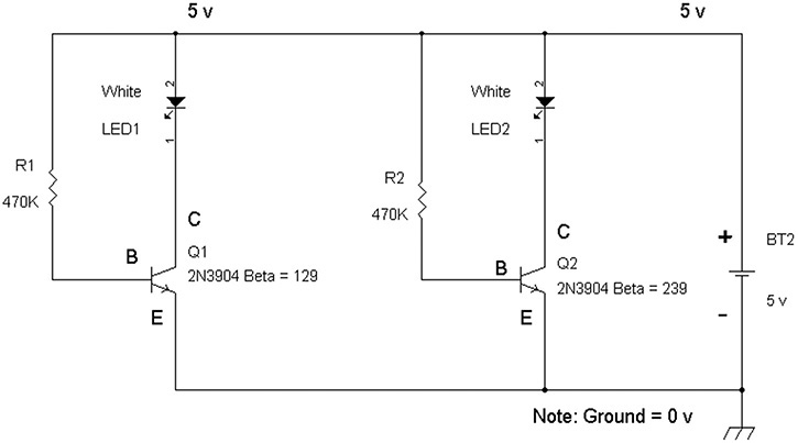
FIGURE 7.11 A simple LED drive circuit with a different current gain, β, for transistors Q1 and Q2.
The simple LED drive circuit in Figure 7-10 uses the existing collector supply voltage source, BT2, to drive the base resistor, R1. The base current with BT2 = 9 volts is then IB = (BT2 – 0.7 volt)/R1 and the LED current, which is the collector current, is then IC = ILED = βIB = β(BT2 – 0.7 volt)/R1.
For example, if β = 50 and R1 = 50KΩ, then:
ILED = β(BT2 – 0.7 volt)/R1 = [50 (9 – 0.7)/50,000] amp = [8.3/1000] amp = 0.0083 amp
or
ILED = 8.3 mA
The current gain in the simple circuit in Figure 7-10 can vary if you have the same part number transistors, such as 2N3904. Figure 7-11 shows an illustration where the β for Q1 = 129, and for Q2 β = 239.
Because of the two different current gains, β = 129 and β = 239 for transistors Q1 and Q2, the LED currents for LED1 and LED2, ILED1 and ILED2, are proportionally different as well.
ILED1 = β(BT2 – 0.7 volt)/R1 = [139(5.0 – 0.7 volt)/470,000] amp or ILED1 = 0.00127 amp = 1.27 mA
ILED2 = β(BT2 – 0.7 volt)/R1 = [239(5.0 – 0.7 volt)/470,000] amp or ILED2 = 0.00218 amp = 2.18 mA
The result of the current gain variation causes a change in LED brightness. See Figure 7-12.
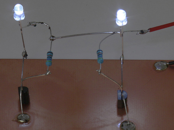
FIGURE 7.12 The circuit built from Figure 7-11 shows that the LED on the left side via Q1where β = 139 is dimmer than the LED on the right side via Q2 where β = 239.
Improved Current Source Circuits
We can improve current source circuits to be less dependent on the current gain β by adding an emitter series resistor, RE, as shown Figure 7-13.
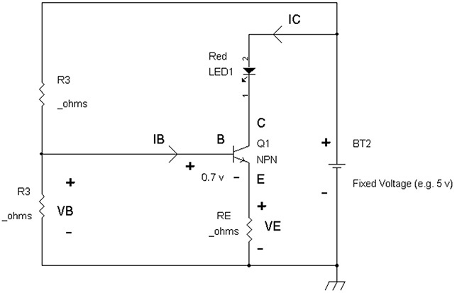
FIGURE 7.13 An improved circuit that is not β dependent to set the collector or LED current.
The collector current or LED current is just the emitter current IE = VE/RE because in a transistor the collector and emitter currents are essentially equal when used as a current source or amplifier circuit.
ILED1 = VE/RE
Resistors R2 and R3 form a voltage divider circuit that provide a base biasing voltage.
VB = BT2 [R2/(R2 + R3)]
To find VE, note that:
VB = VBE + VE
VBE is the voltage across the base and emitter of Q1. As shown in Figure 7-13, VBE = 0.7 volt.
VB = 0.7 volt + VE
Or put in another way in terms of VE:
VE = VB – VBE
VE = VB – 0.7 volt
We need to have VB greater than the turn-on voltage of Q1, which is 0.7 volt. But how much greater should we set it to? It depends on how much voltage we set for the emitter to ground voltage, VE. Typically, we want at least 0.5 volts so that any different lot of transistors with a 0.5-volt to 0.8-volt base emitter turn-on voltage will still work. But a rule of thumb would be something like VE ≥ 0.7 volt.
Because VB = 0.7 volts + VE, and VE ≥ 0.7 volt:
VB = 0.7 volt + ≥ 0.7 volt
VB ≥ 1.4 volts
For example, suppose we want VB = 1.7 volts with BT2 = 5 volts, which means VE = VB – 0.7 volt or VE = 1.0 volts. Or in general:
ILED1 = VE/RE
Or put in another way:
RE = VE/ ILED1
For example, if we want 1 mA = 0.001 amp = ILED1, and VE = 1 volt, then:
RE = 1 volt/0.001amp = 1000Ω
Now let’s get back to solving for R2 and R3 when VE = 1.0 volt.
VB = 0.7 volt + VE
That is, if we measure the voltage across the base and emitter (VBE) and then measure the voltage (VE) at the emitter and ground, we will find VB = VBE + VE. VBE ~ 0.7 volt, so for 1-volt VE:
VB = 0.7 volt + 1.0 volt
VB = 1.7 volts
Resistors R2 and R3 form a voltage divider circuit that provides a base biasing voltage with BT2 = 5.0 volts and RE = 1000Ω. Again, in general:
VB = BT2 [R2/(R2 + R3)]
However, via some algebra a more convenient equation can be derived as:
[(BT2/VB) – 1] = R3/R2, and if BT2 = 5.0 volts and VB = 1.7 volts, then we have:
[(5.0/1.7) – 1] = R3/R2
[2.94 – 1] = 1.94 = R3/R2
Or
R3 = 1.94 × R2
Now the question is, which resistors do we choose?
Can we make R2 = 1Ω and R3 = 1.94Ω? Yes, but you will be either burning up the resistors because the current through the resistors will be BT2/(R2 + R3) = 5 volts/2.94Ω = 1.7 amps, or you will be wasting power like crazy.
Power = P = 5 volts × 1.7 amps = 8.5 watts
A general rule of thumb would be to have R2 have the following range:
RE ≤ R2 ≤ 10 RE
So, let’s take an example setting R2 = 10RE:
R2 = 10 × 1000Ω = 10KΩ
and
R3 = 1.94 × R2 = 1.94 × 10KΩ = 19.4KΩ
or
R3 ~ 20KΩ
With the resistor values R2 = 10KΩ, R2 = 20KΩ, and RE = 1000Ω, Figure 7-13’s current source will deliver a reasonably stable 1 mA given the battery voltage is 5.0 volts, even though the β of the transistor may vary 3:1 with a minimum β of 50. This is because the base current of Q1 no longer predominately determines the collector current or LED current. Instead, it is the voltage VE (via VB) that sets the LED current for a given RE resistance value.
We can improve the current source further by “regulating” VB so that it is a constant voltage. See Figure 7-14 that uses a Zener diode as a reference voltage source, Vref.
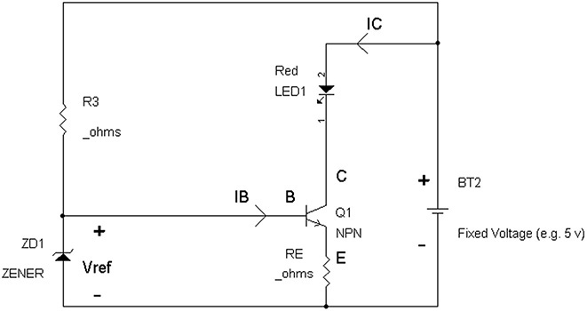
FIGURE 7.14 A Zener diode current source circuit.
In this circuit, first determine the LED current, which is:
VE = Vref – VBE
With
VBE = 0.7 volt
VE = Vref – 0.7 volt
And
ILED1 = (VE)/RE
ILED1 = (Vref – 0.7 volt)/RE
RE = (Vref – 0.7 volt)/ ILED1
As a general rule of thumb, we want the current through R3 to be ≥ 10% of ILED1. For example, we can set the current through resistor R3, IR3 = (BT2 – Vref)/R3 = 10% ILED1, then:
R3 = (BT2 – Vref)/(10% ILED1)
For example, suppose if we want ILED1 = 20 mA, and ZD1 = 1N4371 with a 2.7-volt Zener voltage Vref, then:
In Figure 7-14, there is one precaution to take in terms of making sure the transistor is not in saturation. To ensure that it is really working in the forward active region, we need to have the collector voltage ≥ base voltage, or where the collector voltage is ≥ Vref in this case.
The collector voltage in Figure 7-14 is VC = (BT2 – VLED).
From Chapter 6, we can summarize the following:
• For red, yellow, and most green LEDs, VLED ~ 1.8 volts to 2.0 volts (2.0 volts worse case)
• For blue, white, and green phosphor LEDs, VLED ~ 2.7 volts to 3.0 volts (3.0 volts worse case)
• If Vref = 2.7 volts, then VC ≥ 2.7 volts for a red LED and BT2 = 5.0 volts. (We will use worse case numbers to be on the safe side.)
• Thus, VC = (5.0 volts – 2.0 volts) = 3 volts ≥ VB = Vref = 2.7 volts.
So, we are “fine” using the circuit for red, yellow, and most standard green LEDs.
However, if we use a white or blue LED, VC = (5.0 volts – 3.0 volts) = 2.0 volts, which is less than Vref at 2.7 volts, then the transistor will most likely be in the saturation region. This means that excessive base currents forming a larger than expected voltage drop across R3 will cause Vref to drop and the desired LED current will be lower than expected. Essentially, when the transistor is in the saturation region by having VC < VB, the current gain is no longer β, but some number much less. So how do we fix the problem if we want to put in a white LED for LED1 while not saturating the transistor Q1? One way is by using a 1N4678 1.8-volt Zener diode, which results in Vref = 1.8 volts and RE → 56Ω and R3 can still be 1.6KΩ. The other way with Vref = 2.7 volts is just to raise the battery or power supply voltage to 6 volts or more.
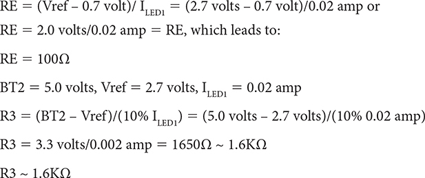
However, in many cases we can replace the 1.8-volt Zener diode with three 1N914 small-signal diodes in series, or use a red LED as shown in Figure 7-15.

FIGURE 7.15 A practical circuit using a red light-emitting diode, LED2 in place of a Zener diode for Vref, a voltage reference source.
Almost any LED can be used as a voltage reference for biasing purposes. Just remember that standard infrared, red, yellow, and green (non-phosphor) LEDs have turn-on voltages of about 1.6 volts to about 2.0 volts. And the blue and white LEDs have about a 2.7-volt to 3.0-volt turn-on voltage. The LED turn-on voltage is then used to provide a reference voltage for biasing.
Figure 7-15 shows a red LED as a voltage reference source to supply about 1.7 volts = Vref. The emitter voltage, VRE = 1.7 volts – 0.7 volt (VBE) ~ 1.0 volt across resistor RE. The voltage, VRE, across resistor RE then sets up the transistor’s emitter current. And essentially the emitter current is equal to the collector current, which in turn is the current flowing through LED1.
If RE = 100Ω, then the LED current is 1.0 volt/100Ω = 10 mA = IC = ILED1. Now if we work backwards to determine the base current, IB, that is equal to IC/β. And if β = 50, IB = 0.01amp/50 = 0.2 mA = IB. With BT2 = 5 volts, the current flowing through R3 is [5.0 volts – VLED2] divided by 1600Ω. With VLED2 = 1.7 volts, we have 3.3 volts/1600Ω = 2.06 mA = current flowing through R3. We can think of the current flowing through R3 branches out to two DC currents:
• A current flowing into LED2, ILED2
• And a current flowing into the base of transistor Q1, IB
We know that the base current, IB = 0.2 mA = IC/β = 0.01amp/50, when β = 50.
Of that 2.06 mA flowing through R3, 0.2 mA goes to the base of Q1 via IB, while the remaining current, ILED2, flows into LED2. To find ILED2, we know that:
3.3 volts/1600Ω = 2.06 mA = current flowing through R3 = IB + ILED2
2.06 mA = IB + ILED2
But IB = 0.2 mA, so:
2.06 mA = 0.2 mA + ILED2
By algebra, subtracting 0.2 mA from both sides of the equation:
2.06 mA – 0.2 mA = ILED2
ILED2 = 1.86 mA
The main thing to take away from this is that there is sufficient current to turn on LED2. Generally, any LED current between 0.5 mA and about 20 mA will work fine.
What Happens When Things Go Wrong
Probably the most common mistakes in LED, diode, or transistor circuits, are reversed component connections. We will look at some examples and see what this will do to other parts of the circuits, starting with Figure 7-16.
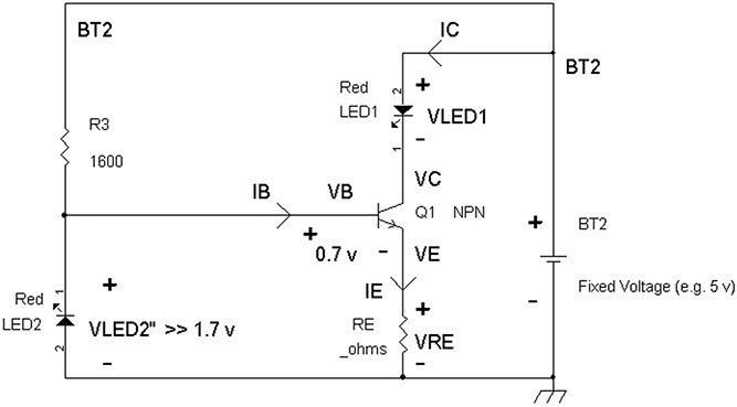
FIGURE 7.16 Voltage reference LED2 is reversed and can cause LED1 to burn out.
With LED2 connected in “reverse bias” mode, it will not light up and it is essentially an open circuit that causes VLED2" >> 1.7 volts. This means that BT2’s voltage via resistor R3 will supply Q1’s base voltage, VB, which will be much higher than 1.7 volts. With VB >> 1.7 volts, the LED1 current ILED1 = (VB – 0.7 v)/RE and LED1 will have excessive current flowing through it. For example, if RE = 75Ω and VB is supposed to be 1.7 volts but someone inadvertently reversed the leads and VB → 3.3 volts via R3, then:
ILED1 = (VB – 0.7 v)/RE = (3.3 v – 0.7 v)/75Ω = 34 mA, for the reversed LED2 connection
The actual voltage VB when LED1 is reverse biased is difficult to calculate offhand because we often do not know the actual β of Q1. Also, the voltage of BT2 enters into this calculation. As a troubleshooter, we do not have to “bother” with trying to figure out the circuit analysis for an incorrectly wired circuit. We just need to solve the problem and restore the circuit back to proper operation. That is, don’t waste too much time analyzing circuits with mistakes. We have to get it working and move on.
To fix this, you connect LED2 properly (LED2 anode to base Q1, and LED2 cathode to ground; the LED’s long lead = anode) as shown in Figure 7-15, and then VB ~ 1.7 volts so that:
ILED1 = (VB – 0.7 v)/RE = (1.7 v – 0.7 v)/75Ω = 13.3 mA
Now let’s look at Figure 7-17 with Q1’s collector and emitter leads reversed.
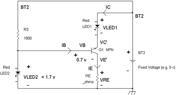
FIGURE 7.17 With Q1’s emitter and collector leads reversed, the current gain is very low with β ≤ 4.
With the collector and emitter leads reversed, transistor Q1 has low β and starts pulling extra current via resistor R3. This causes a large voltage drop across R3, which is IB × R3. For example, if RE = 100Ω and β =2 (due to having the emitter-collector terminals reversed), then what is VB? It has to be lower than 1.7 volts, which will mean that LED2 does not turn on due to the low β = 2. We can approximate VB as follows: If the desired voltage, VB = 1.7 volts, then VRE = 1.7 volts – 0.7 volt = 1 volt, then the desired emitter current is 1 volt/100Ω = 10 mA.
NOTE: For small values of b, generally b < 10, we will need to use the more exact equations relating IB and IC and IE. They are: IE = (b + 1)IB, IB = IE/(b + 1), and we still have IB = IC/b, which leads to: IC = IE [b/(b + 1)]. For example, if b = 9, IC = IE [9/(9 + 1)] = IE(0.90).
If IE = 10 mA and β = 3, then the base current:
IB =10 mA/(β +1) = 10 mA/(3 + 1) = 10 mA/(4)
IB = 2.5 mA
Thus, the voltage drop across R3 = 1600Ω × 2.5 mA = 4.0 volts. VB = BT2 – (voltage drop across R3). VB = 5 volts – (4.0 volts) = 1 volt. At 1 volt = VB, this means that LED2 does not turn on due to LED2’s turn-on voltage being 1.7 volts. This leaves VRE = VB – 0.7 volt = 0.3 volt.
The emitter current IE = 0.3 volt/100Ω = 3 mA.
The “exact” collector current IC = IE [β/(β + 1)] = 3 mA [3/(3 + 1)] IC = 3 mA [3/4] = 3 mA (0.75).
IC = ILED1 = 3 mA (0.75) = 2.25 mA, which is smaller than the 10 mA of LED1 current if the transistor Q1 was correctly connected.
There are two things to take away from connecting the transistor incorrectly in Figure 7-17.
• The reference voltage light-emitting diode LED2 may go dim or turn off.
• The LED1, which is expected to be driven with 10 mA, will be driven with a lower current and will give out much less light.
There are times when we assume that the transistor’s pin out has an order of emitter, base, and collector (EBC). However, there are some transistors such as PN2222 (EBC) that has a similarly named part number P2N2222 (CBE) that has reversed emitter and collector leads. Generally, in the United States common TO-92 plastic case transistors such as 2N3904, 2N3906, 2N4124, and 2N4126 have emitter, base, collector pin outs (EBC). Whereas often used TO-92 transistors in Europe such as BC213, BC238, BC308, BC547, BC557 have pin outs of collector, base, emitter (CBE).
Now let’s look at another example where a Zener reference diode is reversed (see Figure 7-18).
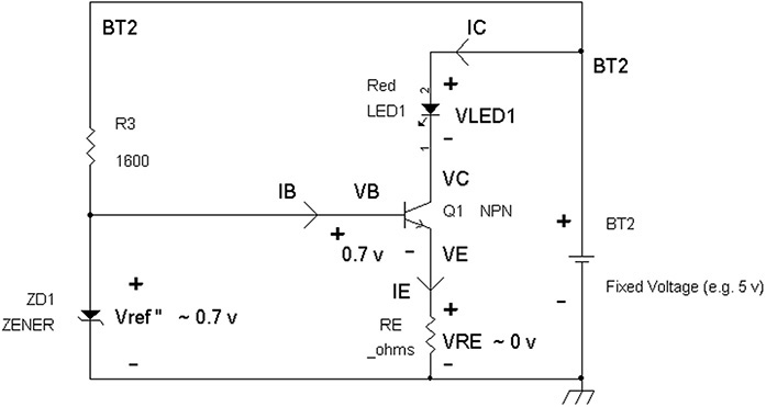
FIGURE 7.18 Zener diode ZD1 is reverse connected, which results in a dimmed LED1.
With a Zener diode connected in reverse, it gives a voltage, 0.7 volt, similar to a forward biased diode. Because of this, VB ~ 0.7 volt, and VRE = VB – VBE, with VBE = 0.7 volt. So VRE = VB – 0.7 volt = 0.7 volt – 0.7 volt ~ 0 volt = VRE. As a result, LED1 is either turned off or being driven with a very small current.
What happens if we reverse LED1’s terminals? We know that it will not light up. But what happens to the rest of the circuit? See Figure 7-19.

FIGURE 7.19 LED1’s anode and cathode leads are reversed, which leads to some very interesting analysis for VB and VE.
We see that with LED1 wired incorrectly, it will not light up. This means it’s essentially an open circuit, which disconnects Q1’s collector lead to any DC path to BT2. See Figure 7-20.
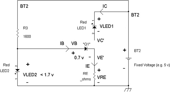
FIGURE 7.20 An equivalent circuit to Figure 7-19 using a diode “model” in place of Q1.
To determine VB, the base-emitter junction of Q1 now acts like a diode. There is no such thing as β or current gain because the collector lead is disconnected. If we make an estimate that VLED2 is less than its turn-on voltage (1.7 volts), then we can safely say that there is no current flowing into LED2. This means the current is flowing from BT2 via resistor R3, diode “Q1”, and RE to ground; and no current flows into LED2.
One way to calculate VB is by finding the current IB flowing though RE. The current, IB, flows into diode “Q1” and it also flows through RE.
Let’s work out a variation of a loop equation. That is the voltage:
BT2 = Voltage across R3 + diode voltage of “Q1” + voltage across RE. The diode voltage of Q1 can be approximated as 0.7 volt.
If you use a volt meter and try measuring BT2 first and then measure the voltages across R3, “Q1” diode, and RE, you will find that summing up all the voltages across R3, “Q1” diode, and RE will equal the voltage of BT2 = 5 volts.
With the following:
• Voltage across R3 = IB × R3
• Voltage across RE = IB × RE
• Diode voltage of “Q1” = 0.7 volt (see Figure 7-20)
we can now solve for IB, and once that is done we can find IB × RE = VRE, which will lead to VB = 0.7 volt + VRE.
Let BT2 = 5.0 volts, R3 = 1600Ω, and RE = 100Ω.
BT2 = IB × R3 + 0.7 volt + IB × RE
5.0 volts = IB × 1600Ω + 0.7 volt + IB × 100Ω
5.0 volts – 0.7 volt = IB 1600Ω + IB × 100Ω = IB (1600Ω + 100Ω) = IB × (1700Ω) = 5.0 volts – 0.7 volt = 4.3 volts
4.3 volts = IB (1700Ω) or by dividing by 1700Ω on both sides of the equation:
(4.3 volts/1700Ω) = 2.53 mA = IB
IB × RE = VRE = 2.53 mA × 100Ω = 0.253 volt = VRE
VB = 0.7 volt + VRE = 0.7 volt + 0.253 volt
VB = 0.953 volt
And as confirmed, VB is less that the 1.7 volts that is needed to turn on LED2.
Insufficient “Headroom Voltage” for the Transistor
We now need to discuss the limitations of transistor current sources. This means we need to pay attention to the collector-base voltage. See Figure 7-21.
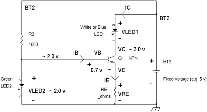
FIGURE 7.21 An LED drive circuit on the “edge of disaster” due to VC ~ VB. If BT2’s voltage drops slightly (e.g., by ~ 0.5 volt), the circuit will start to fail. For proper operation, it is preferable that the collector voltage VC is greater than the base voltage VB, or in other words VC > VB.
In Figure 7-21, as shown, the LED2 voltage is about 2.0 volts = VB, and we replaced LED1 with a blue or white LED, which has a turn-on voltage of 3.0 volts. This means the collector voltage:
VC = BT2 – VLED1 = 5.0 volts – 3.0 volts
VC = 2.0 volts
Generally, to play it safe, VC ≥ VB. In this case, the LED circuit is still workable. However, if the battery voltage, BT2, drops from 5.0 volts to 4.5 volts, then VC = 4.5 volts – 3.0 volts = 1.5 volts. This means VC < VB, or in other words, VB > VC. When VB > VC, the transistor Q1 is either approaching the saturation region, or is already in the saturation region. For current source and amplifying circuits, we want to avoid transistors with these conditions because the β will start dropping.
So, one fix to Figure 7-21 is to lower VB while maintaining a “reasonable voltage” at VE (e.g., VE ≥ 0.5 volt). See Figure 7-22.
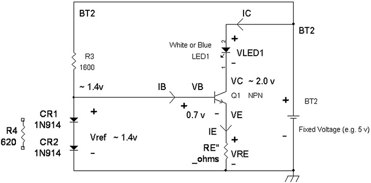
FIGURE 7.22 Base voltage VB is lowered by replacing the green LED 2-volt reference voltage with a lower one at 1.4 volts via two series connected diodes, CR1 and CR2.
With this modification, VB = 1.4 volts, while VC = 2.0 volts. Note that the 1.4 volts developed by these two diodes stay relatively constant should BT2 drop in voltage to 4.5 volts.
Hence, even if BT2 drops to 4.5 volts, VC = 1.5 volts > VB = 1.4 volts, which provides a little safety margin.
Alternatively, the two diodes may be replaced with a 620Ω resistor, R4, to provide 1.4 volts for BT2 = 5.0 volts. However, VB will drop proportionally with BT2. For example:
BT2 = 5.0 volts → VB = 1.4 volts
BT2 = 90% 5.0 volts = 4.5 volts → VB = 90% 1.4 volts = 1.26 volts
This is because VB ~ BT2[R4/(R3 + R4)], neglecting base current IB, which is reasonable for a β ≥ 50.
Another option to avoid transistor Q1 from going into the saturation region is to simply increase the supply voltage BT2, if possible. For example, in Figure 7-21, where BT2 = 5.0 volt and VB = VC = 2.0 volts, having BT2 → 6.0 volts will result in VC = 6.0 volts – 3.0 volts = 3.0 volts, which is greater than the 2.0 volts of VB.
Sometimes Even a Correct Circuit Goes Bad
So far, we looked at only DC conditions, which is very important in troubleshooting circuits. However, even when the DC bias points should work, there can be other problems. This transistor LED circuit discussed so far acts as both current source circuit, but also as amplifier. See Figure 7-23, which can self-oscillate at a very high frequency (e.g., > 100 MHz).
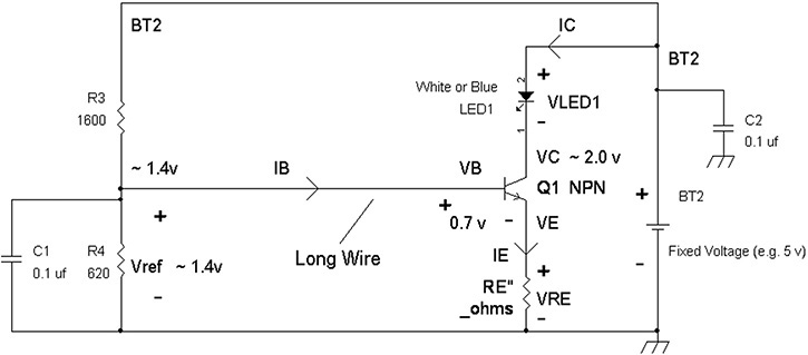
FIGURE 7.23 A current source circuit that can oscillate at very high frequencies due to a long base lead.
Usually, this circuit will work fine. But if you replace the transistor Q1 with a much higher frequency device, such as a VHF (very high frequency) transistor (e.g., MPSH10 whose ft > 600 MHz), the circuit may oscillate at a very high frequency that causes a variation in LED1’s drive current when you touch the base lead.
A long wire connected to Q1’s base behaves like an inductor, which forms a resonant circuit with stray and parasitic capacitances included in the transistor. This can inadvertently form an oscillator circuit. To stop the “parasitic” oscillation, we have to make a lossy inductor by adding a series resistor. See Figure 7-24.
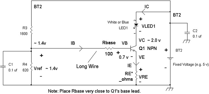
FIGURE 7.24 A series base resistor, Rbase is added in series to the terminal of Q1 to prevent parasitic oscillations.
Rbase usually has a value of 22Ω to 220Ω and should have very short leads itself. And Rbase should be soldered or placed very close to Q1’s base lead. The objective is to prevent the base lead of Q1 from being connected to a long wire.
Figure 7-24 also shows decoupling capacitors to ground, C1 and C2. Generally, you put a decoupling capacitor at your circuit that is receiving the power supply voltage. C2 is added at the circuit near LED1, and not at BT2, which can be connected via long wires that behave like inductors. Decoupling capacitor C1 is placed across the voltage divider circuit R4 and R3 to reduce any high-frequency noise. Generally, most decoupling capacitors have values between 0.01 μf to 2.2 μf.
Summary
We have presented many circuits showing how the transistor works in a current source circuit. Also, several troubleshooting techniques have been illustrated. The gist of troubleshooting is to learn by experience more so than try to be an engineer and analyze everything. Basically, troubleshooting is detective work. You will need to look up data sheets to find the pins outs, but also other specifications like maximum current or voltage that the device can take before breakdown.
Chapter 8 will continue with simple transistor amplifiers based on the LED drive circuits.