CHAPTER 11
![]()
Troubleshooting Analog Integrated Circuits
We will be exploring various types of circuits and systems that use analog integrated circuits as examples of troubleshooting, debugging, and improving. Many of the circuits shown in this chapter will have come from the web (world wide web) or from magazine articles or books. When we build hobby circuits, or fix commercially manufactured products, generally one would assume that the circuits are reliable in terms of performance/design with replaceable parts. From my experience building hobby circuits, working in repair shops or radio stations, and teaching students, I have found that troubleshooting circuits can be broken down into the following categories:
• There are some circuits that will not work or will not work very well as shown in the schematic. These circuits will require some redesigning.
• There are some circuits that will work as a “one of a kind” but may not be repeatable due to the design. This type of design sometimes works by luck. For example, a photodiode circuit seems to work if a minimum amount of light falls on it because the op amp may not have the capability to output down to 0 volts but have to start at about +1 volt (e.g., see Figure 11-18).
• Many circuits published really do work. And these circuits will perform fine as shown in the schematics or instructions. However, sometimes it may be “easy” to mis-wire a circuit or put in the wrong part. Other times, the circuit may work in “normal” consumer everyday use but will break down under 24/7 schedules due to overheating, for example. Using a higher-power device can fix this problem.
We will concentrate on the first two categories—circuits that are redesigned for more reliable operation.
Circuits That Need Fixing or Redesigning
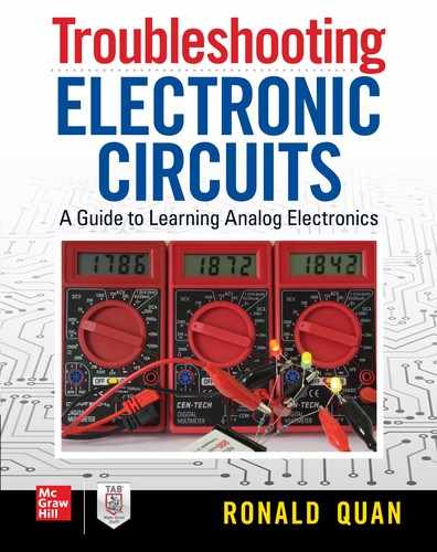
Let’s take a look at a problem I had to solve just recently when a young student showed me a preamp circuit lifted off the web for amplifying electric guitar pickups. See Figure 11-1.
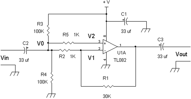
FIGURE 11.1 A preamp meant to have a gain ~ 30 but instead has a gain of 1.
As we can see, Figure 11-1 shows some good points in that the DC bias voltage is correct to provide one-half the DC supply voltage, V0, from R3 and R4. Via V0 connected to R5 and R2, the op amp’s output pin will be biased to one-half the DC supply voltage for maximum AC voltage swing. With a 30KΩ R1 feedback resistor and a 1KΩ R2 input resistor, at first glance, the (inverting) voltage gain should be –R2/R1 = –30K/1K = –30, correct? No. Because the input signal also is coupled to the non-inverting input pin 3, there is a gain cancellation effect going on. The reason is any input signal at the (+) input of op amp with the same input voltage at R2 results in a non-inverting amplifier’s gain summed with the inverting gain.
Note that the input resistance into the (+) input terminal, V2, is very high so there is “no” current flowing through R5, which means there is no voltage across R5, or R5 may as well be a short circuit or 0Ω wire. The reason is because V0 = V2, and since V2 at the (+) input terminal acts as a reference voltage for the feedback amplifier, the (–) input voltage V1 must follow the same voltage as V2. Thus V1 = V2, and since V0 = V2, V0 = V1. This means the voltage across R2 is 0 voltage and the input resistance to R2 (e.g., at V0) is infinite resistance since 0 volts across R2 implies there is no current flowing through R2.
When the input resistor R2 (left side) is connected to the (+) input (via R5) we have the following:
The non-inverting gain is [1 + (R1/R2)]; and the inverting gain is –(R1/R2).
The total gain (AC or DC signal) is then [1 + (R1/R2)] + –(R1/R2), which leads to: 1 + (R1/R2) – (R1/R2) = 1 = the total gain = non-inverting gain plus inverting gain.
This total gain makes sense in terms of the DC gain as well. Since R3 and R4 form a voltage divider of half the supply voltage at R5 and R2, with a gain of 1, the DC output voltage at pin 1 of the op amp has to be one-half the supply voltage. For example, if +v = 9 volts, pin 1 = 9 volts/2 or 4.5 volts DC.
So how do we fix this circuit to have gain? See Figure 11-2, where we add C5.
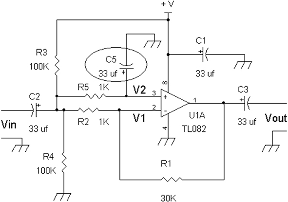
FIGURE 11.2 By adding C5, we provide an AC short to ground at the non-inverting input pin.
By AC shorting to ground the non-inverting input (pin 3) via adding C5, we now have a “standard” inverting gain amplifier that has a gain of Vout/Vin = –R1/R2 = –30K/1K or Vout/Vin = –30. The preamp is restored to a reasonable gain for amplifying the guitar pickup’s signal. R1 may be increased further to increase the gain, such as having R1 = 100KΩ for a gain of –100.
If we look at the AC input resistance, Rin, of this preamp in terms of Vin “looking” into C2, we see that C2 and C5 are AC short circuits, so we have the following pertaining to Figure 11-2.
R3’s top connection is connected to +V, an AC ground, so AC-wise R3 is in parallel with R4. Because C5 acts as an AC short to ground, R5, which is connected to C5, is grounded as well. This means the AC input resistance has at least R3 in parallel with R4 and R5. Because the (+) input is AC grounded via C5, we know that the input resistance of an inverting op amp circuit is just the input resistor, which is R2. Thus, the AC input resistance is then R3 in parallel with R4, R5, and R2. Or, Rin = R3||R4 || R5 || R2. We can group the equal value resistors together since R3 = R4 = 100kΩ, and R5 = R2 = 1kΩ.
Rin = (R3||R4) || (R5 || R2)
Since R3||R4 = 100kΩ||100kΩ or R3||R4 = 50KΩ, and R5||R2 = 1kΩ||1kΩ or R5||R2 = 500Ω, Rin = 50kΩ||500Ω. However, Rin ~ 500Ω, since 50KΩ >> 500Ω.
In this first fix in Figure 11-2, the gain was restored, but R5 added to the loading input source, Vin. We can rescale the values for R5 and C5 to increase the input load resistance at Vin. See Figure 11-3.
FIGURE 11.3 We can scale R5 up 100x and also use a smaller value C5 to provide an AC short circuit to ground.
By rescaling the values of R5 and C5, we mean having the time constant R5 × C5 of Figure 11-3 equal to or greater than R5 × C5 of Figure 11-2. The reason for this is so that C5 in both Figures 11-2 and 11-3 will be an AC short circuit to ground relative to R5.
In Figure 11-2, the resistor-capacitor time constant R5 × C5 = 1KΩ × 33 μf = 0.033 second; and in Figure 11-3, R5 × C5 = 100KΩ × 1 μf = 0.10 second > 0.033 second, so we are OK with this rescaling. A larger time constant means we have more filtering from noisy power supplies at +V. In general, C5 should be at least 0.1 μf. That is, if you scale R5 to 10MΩ and C5 to 0.01 μf, the preamp will work providing the circuit is enclosed in a shielded and ground metal box because pin 3 of the op amp will not have a low enough impedance at 50 Hz or 60 Hz and may pick up hum from power lines.
Given the rescaled values for R5 and C5, the input resistance now is:
R3||R4||R5||R2 = (R3||R4||R5) || R2
With R3 = R4 = R5 = 100KΩ, (R3||R4||R5) = 100KΩ/3 = 33.3KΩ, which is >> R2 = 1KΩ. Thus, Rin ~ 1KΩ in Figure 11-3 versus Rin = 500Ω in Figure 11-2.
Can we improve this circuit further and why? If the power supply is from a battery, there will not be a problem in terms of noise induced to the input via R3 and R4. However, if +V is from a power supply with some noise such as power supply ripple, the power supply noise may be coupled to the output of the op amp. See Figure 11-4 for a further improved circuit to reject power supply noise and maintain maximum input resistance for an inverting gain op amp circuit.
FIGURE 11.4 An improved circuit to further reject power supply noise.
By connecting the DC biasing circuit R3 and R4 with C2, a low-noise DC bias voltage is established at the non-inverting input terminal of the op amp. Since R3 and R4 are equal in value, the DC voltage is one-half +V. Thus, we get one-half the supply voltage at the (+) input terminal of the op amp and because of R1, the DC bias voltage at the (+) input terminal “forces” the same voltage at the (–) input terminal. And because there is no DC current flow through R1 (recall input bias current → 0), the voltage across R1 = 0 volts. Thus, the DC output voltage at pin 1 is also one-half the supply voltage, which is (+V/2). Again, DC-wise, R2 is “disconnected” since C4 is an open circuit at DC.
The values of R3, R4, and C2 were chosen to form a low-pass filter with a very low-frequency cut-off as to substantially reduce any power supply ripple from +V. With R3 = R4 = 100KΩ and C2 = 33 μf the cut-off frequency, fcut-off = fc:
fc = 1/[2π(R3||R4)C2] = 1/[2π(100KΩ||100KΩ)33μf] or fc = 0.0965 Hz ~ 0.10 Hz
To find the attenuation factor of a noise signal at a frequency fnoise, we have:
attenuation factor = fc/fnoise = 0.1 Hz/fnoise
For example, if we have a 60-Hz signal at 10 mV peak to peak riding on top of +V, then the AC signal at the (+) input will be 10 mV peak to peak × (fc/fnoise), which is then 10 mV peak to peak × (0.1 Hz/60 Hz) = 0.0166 mV peak to peak. If more filtering is required, you can increase the values of the resistors R3 and R4 to about 1MΩ with C2 = 33 μf, but it will take about 60 seconds or so for the bias voltage to come up to one-half +V.
Note that even though there is the ripple voltage at the op amp’s power pin 8 with +V, the op amp itself has sufficient power supply ripple rejection to prevent this ripple voltage from feeding through to the op amp’s output pin 1.
If we are concerned with low input resistance, Rin, and power supply noise, one of the best moves is to use a non-inverting gain configuration. See Figure 11-5, which is configured for a higher input resistance at C2.
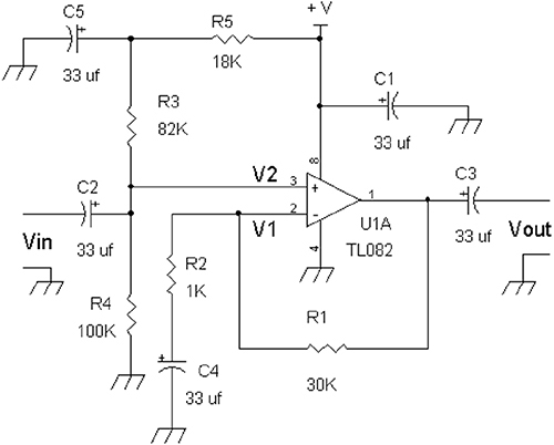
FIGURE 11.5 A non-inverting gain amplifier with extra power supply filtering via R5 and C5.
By using a non-inverting amplifier for a preamp, we have the advantage of larger input resistance, Rin, which is equal to R4||R3 = 100KΩ||82KΩ or Rin = 45KΩ, due to C5 being an AC short circuit to ground. Again, if more filtering from noise via the power supply, +V, is required, C5 can have a larger capacitance such as 330 μf. Generally, a TL082 op amp will be “good” enough low noise-wise for some low-level sources such as magnetic pickups or microphones.
However, you can make a lower noise preamp if the low-level source includes a low impedance device such as a dynamic microphone. In Figure 11-5, you can replace U1A with a lower noise op amp such as an OPA2134, LM833, or NE5532, and rescale the feedback network, R1, R2 for lower resistances such as:
R1 = 3000Ω, R2 = 100Ω, and C4
to a larger capacitance value to maintain good low-frequency response such as C4 = 330 μf.
We now will look at a circuit found off the web or a hobby book. See Figure 11-6, which shows a high-gain op amp circuit that drives a speaker amplifier.
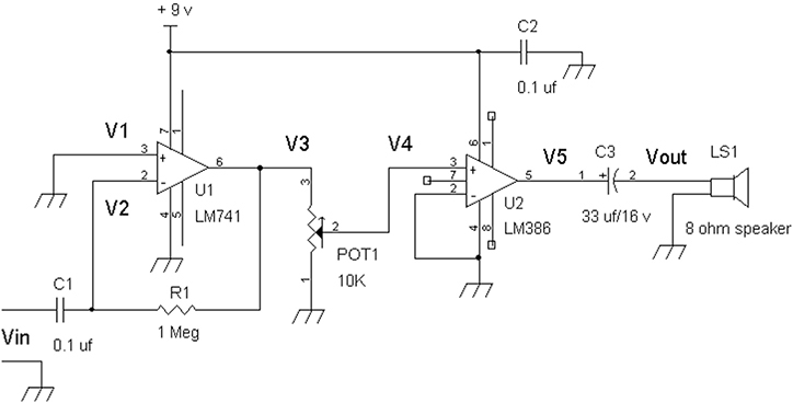
FIGURE 11.6 An amplifier circuit that kind of works, which produces distorted signals.
This amplifier has a basic flaw in that U1 LM741 really requires a negative power supply to pin 4. Also, the other problem with this amplifier is that a DC voltage from the LM741’s output pin 6 couples a DC voltage to the input terminal of U2, LM386. In general, the LM386’s input terminal wants to see an AC coupled signal with no DC component.
As a result of pin 4 grounded for U1, the output signal resembles an amplified half-wave rectifier. See Figure 11-7.

FIGURE 11.7 Top trace is the output signal at about 5.7 volts peak to peak; bottom trace is the input signal at about 124 mV peak to peak.
We can show a way to slightly redesign the circuit in Figure 11-6 to solve the problems previously mentioned.
See Figure 11-8 where C5 along with R2 and R3 are added. Please refer to the redesigned circuit in Figure 11-8.
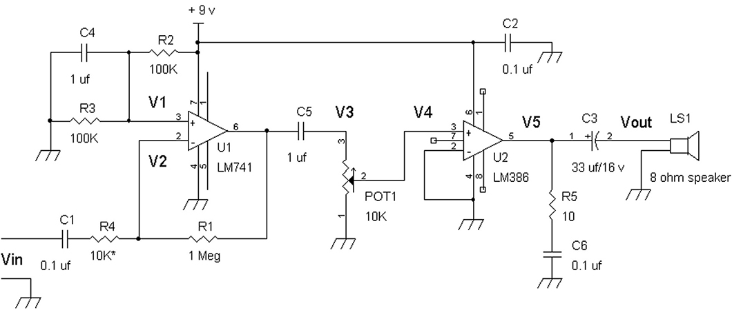
FIGURE 11.8 A “fixed” version with an extra bias circuit, R2 and R3, which allows the circuit to work off a single supply.
We can add a minus power supply (e.g., –9 volt) to pin 4, however, a little re-biasing of the LM741’s input stage should fix our problem. See Figure 11-8.
To debug Figure 11-6, we “un-ground” the non-inverting input pin 3 of U1 and provide it a one-half supply voltage at 4.5 volts. C4 is added to reduce noise from the +9-volt supply. Input capacitor C1 is now connected to a series resistor R4 to provide an inverting gain op amp circuit, where the gain of U1 is – R1/R4. If more or less gain is required, the resistance value of R4 may be varied, such as from 1000Ω to 100KΩ. If a better low-frequency response is needed, C1 can be replaced with a 33-μf (25-volt) capacitor with its positive terminal connected to R4 (Figure 11-8).
In Figure 11-6 the signal was coupled directly via C1 to the inverting input terminal, which made the op amp work in an “open” loop configuration. When an op amp is operating in an open loop configuration, it is behaving more like a comparator and the output signal is more like either on or off. Now see Figure 11-8.
To ensure that no DC voltage appears at the input of U2, an extra coupling capacitor C5 is added in series with POT1. Finally, a snubbing network, R5 and C6, is added at the output of the LM386 pin 5 to ensure that no parasitic high-frequency oscillation occurs as recommended in the LM386’s data sheet.
Other improvements to this circuit can include changing output speaker capacitor C3 to a larger capacitance value, such as 100 μf to 220 μf (16 volt).
If a “faster” op amp is needed in terms of gain bandwidth product (GBWP) for U1, the LM741 (1 MHz GBWP) may be replaced with a TL081 (3 MHz GBWP), LF351(4 MHz GBWP), or OPA134 (8 MHz GBWP).
Our next circuit that needs debugging is an active band pass filter that can be used for audio signal applications such as an equalizer, or for applications where you want to pass a signal around a center frequency while attenuating signal whose frequencies are outside the center frequency.
For example, if you like to “isolate” a 19-kHz signal that has been added to a high-fidelity audio whose frequency ranges from 50 Hz to 15 kHz, an active band pass filter can be used. It will pass the 19-kHz signal essentially without attenuation, while removing most of the signal from 50 Hz to 15 kHz.
In Figure 11-9 there are two graphs of a lower Q band pass filter and a higher Q band pass filter. Notice that the higher Q filter is narrower in shape, which allows for better rejection of signals whose frequency is outside of the center frequency fc. A good approximation for Q is the center frequency divided by the –3 dB or 70.7 percent amplitude frequencies. That is Q = fc/BW–3 dB.
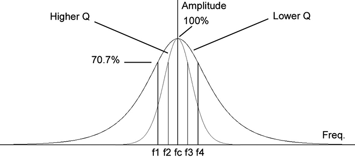
FIGURE 11.9 Graphs of band pass filters relating to –3 dB (at 70.7 percent) points and Q.
For the lower Q band pass filter: Q = fc/(f4 – f1) where (f4 – f1) = –3 dB bandwidth; and for the higher Q band pass filter: Q = fc/(f3 – f2) where (f3 – f2) = –3 dB bandwidth.
For example, if the center frequency, fc = 10 kHz and f3 = 10.5 kHz with f2 = 9.5 kHz, then the higher Q band pass filter has:
Q = 10 kHz/(10.5 kHz – 9.5 kHz) = 10 kHz/1kHz or Q = 10
If the lower Q band pass filter has f4 = 11 kHz and f1 = 9 kHz, and recall that fc = 10 kHz, then its Q = 10 kHz/(11 kHz – 9 kHz) = 10 kHz/2 kHz or Q = 5.
The graph in Figure 11-9 overlays the “normalized” curves of the lower Q and higher Q band pass filters. In reality, often the higher Q band pass filter will have more gain at the center frequency when compared to the lower Q band pass filter. For example, if the higher Q band pass filter provides 2 volts AC at fc, then the lower Q band pass filter may provide 1 volt AC at fc. Note: On the next page fcenter = fc.
Now let’s take a look a band pass filter that does not work with AC signals. See Figure 11-10.
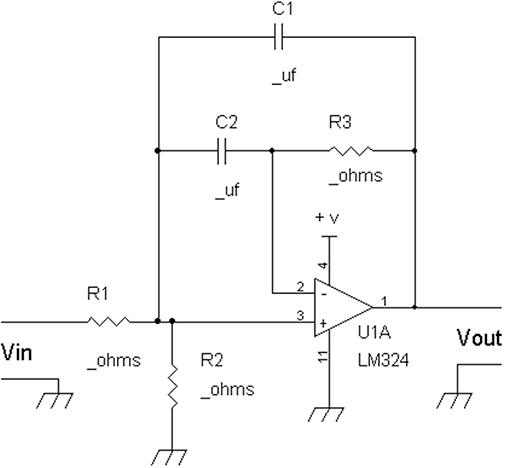
FIGURE 11.10 Example wrong active band pass circuit that has DC biasing problems at the Vin input terminal with R1.
The band pass filter in Figure 11-10 would work if the minus supply pin 11 that is connected to ground would be instead connected to a negative power supply such as –9 volts. As a result of having the negative supply pin 11 connected to ground, the op amp is not capable of outputting a signal that swings below ground. Also, the non-inverting input at pin 3 cannot tolerate a signal below –0.5 volts. So again, an AC signal connected to Vin will produce a distorted Vout. Also note that the LM324 is known for crossover distortion, so using that op amp is not the best choice along with its low gain bandwidth product of 1 MHz. This bandpass filter can run the limit of an op amp’s gain bandwidth product because it is “gain hungry.” For example, suppose we want to build a 19-kHz bandpass filter with a –3 dB bandwidth of 2 kHz. This means at 1 kHz below and above the center frequency, 19 kHz, the response is 70.7 percent of the peak amplitude at 19 kHz. This means at 18 kHz and 20 kHz these are the –3 dB frequencies. The Q of a bandpass filter is defined as Q = fcenter/BW, where fcenter = center frequency of the band pass filter.
With this example, Q = 19 kHz/2 kHz or Q = 9.5.
The gain at the center frequency is Av = 2 Q2.
For this example, Av = 2 (9.5)2 or Av = 180.
To determine the op amp’s open loop gain at 19 kHz, an approximation is GBWP/ fcenter.
For the LM324 that has a 1 MHz GPWP, the open loop gain at 19 kHz ~ 1 MHz/19 kHz ~ 52.
Note that we need at least 180, and generally we want the open loop gain to be about 4 to 10 times of Av = 2 Q2. That is, we want the op amp’s open loop gain at 19 kHz to be 720 to 1800.
For example, an LT1359 Quad op amp with 25 MHz GBWP would work, having an approximate gain of 25 × 52 = 1300 at 19 kHz.
Sometimes it’s better to use dual op amps rather than quad op amps. The reasons are a wider selection, lower cost, and a greater chance to find a faster op amp. Now let’s take a look at the debugged version in Figure 11-11.
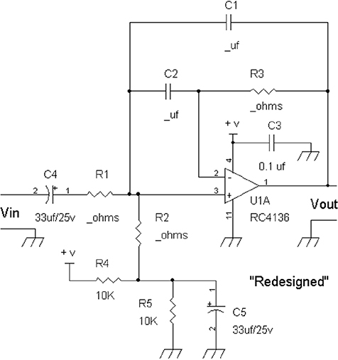
FIGURE 11.11 Corrected band pass filter circuit with a DC bias circuit, R4, R5, and C5.
By adding a bias circuit to form a one-half supply voltage with a large capacitance C5, the circuit is debugged. Also, a different quad op amp, the RC4136, which has a 3 MHz GBWP, is used instead of the LM324. The RC4136 has a very good output stage that does not exhibit crossover distortion.
Because the RC4136 has a 3-MHz gain bandwidth product (GBWP), the band pass filter’s center frequency is limited to Q < 10 and fcenter < 3.75 kHz. A worst case calculation was made by the following:
2 Q2 = 2 (10)2 = 2 (100) = 200
This gain number of 2 Q2 is when R2 is removed from the circuit and R1 drives the band pass filter.
We want an open loop gain of at least 4 times the 2 Q2 at the band pass filter’s center frequency.
The open loop gain required is then 4 × 2 Q2 = 4 × 200 = 800. Now we need to find the band pass filter’s maximum center frequency, fcenter-max:
fcenter-max = GBWP/(4 × 2 Q2) = 3 MHz/800 = 3.75 kHz
To determine the values of the resistors R1, R2, and R3, and the capacitors C1 and 2 for a given band pass filter with a center frequency, fcenter, and Q based on the desired –3 dB bandwidth, see the following:
–3 dB bandwidth = fcenter/Q
R1||R2 = R3/(4 Q2), where also R1||R2 = (R1 × R2)/(R1 + R2)
R3 = Q/(π C fcenter)
C = C1 = C2
The gain of the overall band pass filter is [R2/(R1 + R2)] × 2 Q2.
When the value of Q may be in the order of 3 to 10, this gives a gain range, 2 Q2, from 18 to 200. This means that the band pass filter has quite a bit of gain at the center frequency. To ensure that the band pass filter does not overload too easily, the input resistors R1 and R2 form a voltage divider that will reduce the overall gain. A good starting point for R1 and R2 is to make a voltage divider of about 10:1 or 11:1. For example, in an 11:1 voltage divider, if R1 = 10R2, then [R2/(R1 + R2)] = 1/11; the gain range from Vin to Vout is now reduced to 1.6 to 18 instead of 18 to 200.
One way to start designing the band pass filter is to determine C as a function of R1||R2, Q, and fcenter. We can substitute R3 = Q/(π C fcenter) into R1||R2 = R3/(4 Q2) to express R1||R2 as a function of Q, C, and fcenter, which leads to the following:
R1||R2 = 1/[π C 4Q fcenter]
and now we can find C as a function R1||R2, Q, and fcenter as:
C = 1/[π (R1||R2) 4Q fcenter] = C1 = C2
Once C is determined, we can find R3 via:
R3 = Q/(π C fcenter)
For example: Suppose we want to build a band pass filter having fcenter = 1 kHz with Q = 3, and given that R1 = 100KΩ and R2 = 10KΩ such that R1||R2 = 100KΩ||10KΩ ~ 9.1K.
C = 1/[π (R1||R2) 4Q fcenter] = 1/[π (9.1KΩ) (4)(3) 1kHz] or C = 2916 pf = C1 = C2.
C1 = C2 ~ 2700 pf in parallel with 220 pf or a 0.0027 μf in parallel with 220 pf.
R3 = Q/(π C fcenter) = 3/(π 2916 pf 1 kHz) or R3 = 109KΩ ~ 110KΩ, and to reiterate, R1 = 100KΩ and R2 = 10KΩ.
The overall gain at the center frequency is Vout/Vin = [R2/(R1 + R2)] × 2 Q2 or in this example:
[10K/(100K + 10K)] × 2 (3)2 = [1/11] × 2 × 9 = 18/11 = 1.6 = gain or Vout/Vin = 1.6 @ 1kHz.
Photodiode Circuits
We now turn our attention to photodiode preamps. These are often used with sensor or communication systems. Here we will explore some mistakes as posted on the web or in some hobbyist books.
Photodiode sensors with light sources such as LEDs can be used to sense the presence or distance of an object. Also, photodiodes with a focused light beam can be used to read black and white lines such as bar codes. In this section, we will look at photodiode “receiver” circuits that convert the light sensed into a signal voltage. Let’s first look at a typical photodiode that has a cathode lead and an anode lead along with its associated schematic symbol. See Figure 11-12.
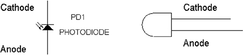
FIGURE 11.12 Schematic symbol of a photodiode (note arrows pointing into the diode whereas in an LED the arrows are pointing away from the diode), and identification via the lead length where the anode lead is slightly longer than that cathode’s lead.
If the leads are the same length, you can use an ohm meter to measure the forward voltage from anode to cathode, which is about 0.7 volts or so. Measure again with a standard diode (1N914) where the cathode is clearly marked with a band, and you should be able to identify the cathode of the photodiode. Now, let’s take a look at what is really a photodiode. See Figure 11-13.
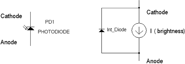
FIGURE 11.13 A photodiode schematic diagram is on the left side, and a current generator representation of it shown on the right hand side with the internal diode, Int_Diode.
The photodiode acts like a light intensity current source, with the positive current flowing from cathode to anode. In a sense it’s like an NPN transistor current source where the current flows from collector to emitter. Hence, the photodiode is polarity dependent. The photodiode current is modeled as “I (brightness)” to depict that it is proportional to light intensity. That is, the more light there is, the higher the current is generated from the photodiode. Typically, the photodiode will generate currents as low as I (brightness) < 0.001 μA when it is covered or in the dark, or with intense lighting such as in sunlight, it will generate I (brightness) >> 1 μA.
In this book, we can also sometimes “shorthand” I (brightness) with I (lum), where “lum” is the luminance level that is the same as brightness. For example, when you buy an LED bulb for a ceiling lamp, it is rated in lumens (e.g., a 9-watt LED lamp equivalent to a 60-watt incandescent bulb gives out about 800 lumens).
Note let’s take a look at some working circuits before we examine non-working ones. A photodiode can be connected to load resistor RL to develop a voltage across it as shown in Figure 11-14.
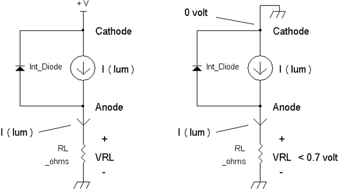
FIGURE 11.14 Two photodiode circuits, one with a +V bias (left side), and the other on the right side with 0-volt bias (via the cathode being connected to ground).
To “extract” the photodiode’s signal, generally it is reverse biased or zero biased to prevent the photodiode’s current from diverting into its internal diode instead of flowing out into a load resistor. As shown in Figure 11-14, we see on the left side’s circuit that +V is forming a reverse bias to the internal diode, Int_Diode. The maximum voltage across RL is VRL = (+V) +0. 7 volt.
For example, if we are using a 5-volt supply, then +V = +5 volts and the maximum voltage across load resistor RL = +5 volts + 0.7 volt = 5.7 volts.
The voltage across the load resistor is VRL = I (lum) × RL and equivalently, I (lum) = VRL/RL.
If, for example, RL = 1MΩ and +V = +5 volts, then the maximum photodiode current, I (lum)max = 5.7 volts/1MΩ or I (lum)max = 5.7 μA.
In Figure 11-14, the circuit on the right shows what happens when +V → 0 volts that essentially grounds the cathode of the internal diode. This means that Int_Diode is now in parallel with RL, and also means it “clips” or limits the maximum voltage across RL by the turn-on voltage of a silicon diode or about 0.7 volt. As an example, if RL = 1 MΩ with +V = 0 volts, I (lum)max = 0.7 volts/1MΩ or I (lum)max = 0.7 μA = 700 nA.
If we want to buffer (amplify) the signal output of Figure 11-14, we can use a voltage follower or non-inverting gain amplifier that can sense at ground and provide an output voltage at near ground, such as a TLC272 op amp. However, there can be a disadvantage by merely amplifying VRL with a non-inverting gain amplifier. Because the RL is typically 100kΩ to 1 Meg ohm, even small stray capacitances can cause a frequency response problem.
For example, if the photodiode has a 10-pf internal capacitance, Cpd, across the cathode and anode, the high-frequency response with RL = 1MΩ will be about 16 kHz where the cut-off frequency, fc = 1/[2π (RL × Cpd)] which is: fc = 1/[2π (1MΩ × 10 pf)] = 15.924 kHz = fc.
We can improve on high-frequency response by using a “trans-resistance” amplifier, which means current in and voltage out. But before we show you some trans-resistance amplifier circuits, let’s take a look at testing the photodiode itself with a digital voltmeter (DVM). See Figure 11-15.
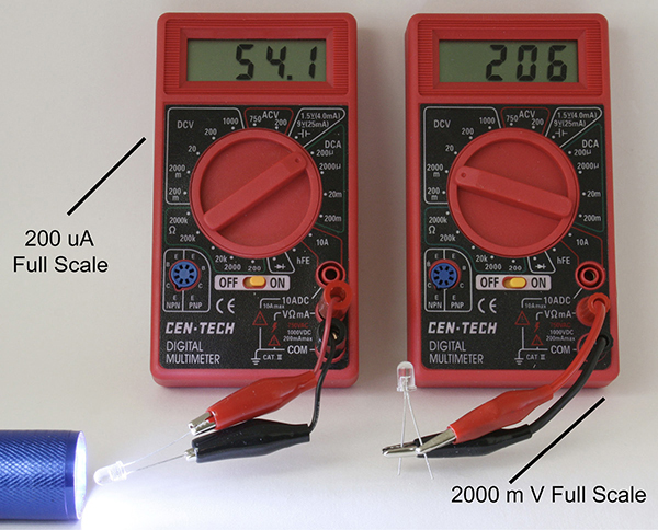
FIGURE 11.15 Two ways to measure photodiodes via the voltmeter (on the right side) and via the current (micro amp meter) settings (on the left side).
Even a typical low-cost DVM can test photodiode via its 200 mV or 2000 mV DC full-scale setting because it has a built-in 1MΩ resistance across the positive and negative leads. You can use a flashlight and shine it directly into the photodiode and read the voltage output with the voltmeter setting. Note that the voltage will be limited to about 700 mV DC. As shown in Figure 11-15, the voltmeter shows 206 mV across the input 1-MΩ input resistance of this particular DVM. This means the photodiode is 206 mV/1 MΩ or 206 nA (nano amps) or equivalently 0.206 μA. If you use a higher input resistance DVM that normally has a 10MΩ input resistance at the voltmeter setting, you can measure the photodiode current with 10x sensitivity.
Also shown in Figure 11-15 is that you can measure the photodiode’s current directly by using the 200 μA full scale setting as shown with a flashlight shining directly into the photodiode measuring 54.1 μA.
If you need to measure lower photodiode currents, such as using a lower sensitivity photodiode or an LED, use a slightly higher-performance DVM with a 10MΩ resistance across the positive and negative leads. With 10MΩ load resistance the sensitivity is increased 10x over the lower priced DVM. For example, most auto-ranging and >$20 DVMs have 10MΩ resistance in the voltmeter mode.
Note if you use an LED as a photodiode, the equivalent internal diode, Int_Diode, as depicted in Figure 11-14 will have a maximum voltage of the LED’s turn-on voltage, VLED. For example, in a red, green, and yellow standard LED, the turn-on voltage is about 1.7 volts. For a blue or white LED, expect the turn-on voltage to be about 2.5 volts to 3.0 volts. This means if you shine light into the LED, the maximum voltage across RL will be VRL ≤ LED’s turn on voltage, which can be in the order of 1.7 volts or more for VRL depending on what type of LED you are using. Also, the pin out will be same for the LED as with the photodiode; the shorter lead will be the cathode.
Trans-resistance Amplifiers
Figure 11-16 shows a trans-resistance amplifier with a photodiode connected to the inverting input of an op amp. The input signal is a current and the output provides a voltage. In terms of “gain” we have a voltage output divided by a current input or V/I that has the unit of resistance.
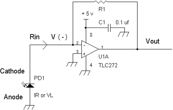
FIGURE 11.16 A trans-resistance amplifier for providing a low-impedance voltage output related to photocurrent from PD1, a photodiode. Note: IR = Infrared and VL = Visible Light.
The photodiode, PD1 in Figure 11-16, has its cathode connected to the (–) input terminal of U1A, which serves as a low resistance point referenced to ground. That is, the input resistance, Rin, looking into the combination of feedback resistor R1 and pin 2, the inverting input of U1A, is very low for two reasons.
The first reason is that since the pin 3 (+) input terminal is grounded (or AC grounded if pin 3 is tied to a +V positive bias voltage), the (–) input terminal must have the “same” voltage as the (+) input voltage due to negative feedback via R1. Thus, Rin is looking into a virtual short circuit to ground via the (+) input being grounded. In actuality, Vout is adjusting the voltage such that the current through R1 matches the photodiode’s current from PD1. When this happens, the voltage at V(–) is “adjusted” to ground or 0 volts via Vout.
The second reason why Rin is close to 0Ω is that in an inverting gain op amp amplifier, the input resistance looking into the inverting input terminal is Rin ~ R1/[A0(f)], where A0(f) = open loop gain of the op amp as a function of frequency. You can also estimate A0(f) by knowing the gain bandwidth product (GBWP) for frequencies beyond the open loop frequency response.
For example, if U1A = TLC272, the gain bandwidth product, GBWP, is about 1.7 MHz for a 5-volt power supply. If we want to know the approximate Rin at f = 100Hz with R1 = 1MΩ, we can estimate A0(f) ~ (GBWP/f), with the understanding that in most cases the maximum A0(f) is between 100,000 and 1,000,000.
Rin = R1/ A0(f) ~ R1/(GBWP/f) = 1MΩ/(1.7MHz/100Hz) = 1MΩ/17,000 or Rin ~ 59Ω. When we consider that PD1 outputs something in the order of 10 μA maximum, the voltage at V(–) will be 10 μA x Rin or V(–) ~ 0.59 mV, which is ~ 0 volts.
Note at DC or slowly changing signals with time, A0(f) is ≥ 100,000. So, given that the open loop gain, A0(f) is ≥ 100,000 at DC or low frequencies, Rin ≤ 1MΩ/100,000 or Rin ≤ 10Ω, which pretty much looks like a short circuit to ground considering PD1’s photocurrents are typically ≤ 10 μA.
You can download op amp spec sheets from various manufacturers (e.g., Texas Instruments, Analog Device, New Japan Radio, ST Electronics, etc.) for open loop gain, A0(f), data.
Now let’s take a look at Figure 11-17. The output voltage Vout = R1 × I (lum), where I (lum) is the photodiode’s current flowing downward from cathode to anode of PD1.
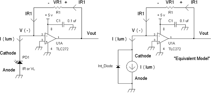
FIGURE 11.17 A trans-resistance amplifier with photodiode PD1 in the left circuit with its “Equivalent Model” on the right side showing a light intensity controlled current source generator, I (lum).
Notice in Figure 11-17 the TLC272 op amp is chosen specifically to work with +5 volts for sensing at 0 volts at the input terminals pins 2 and 3, and also for the ability for the output at pin 3 to swing all the way down to ground. Typically, the feedback resistor R1 is in the range of 100KΩ to 4.7MΩ. For example, if R1 = 470KΩ, then Vout = I (lum) × 470KΩ, which is a positive voltage.
Essentially, how we get the positive voltage for Vout goes like this: We know that no current flows into the (–) input at pin 2 of U1, so this means R1’s current IR1 = I (lum), the photodiode current. When I (lum) starts generating current based on light intensity, it will “pull” current through R1. Since the (+) input terminal at pin 3 is connected to ground or zero volts, the negative feedback system has to correct itself to ensure the (–) input voltage matches the (+) input voltage, which is ground. Thus, the (–) input is “servoed” to ground via Vout and feedback resistor R1. When the light shines in the photodiode, the photodiode’s current, I(lum), forces Vout, then rises to a positive voltage just enough such that Vout/R1 = I (lum). This forms a balanced condition whereby the voltage at R1 connected to the (–) input is now 0 volts, which is what the negative feedback system wants. Essentially, it is saying that it wants the following condition at the (–) input terminal Vout – IR1 × R1 = 0 volts = voltage at (–) input, or put in another way, Vout = VR1 = IR1 × R1.
Since IR1 = I (lum), then we have Vout – I (lum) × R1 = 0 volts at the (–) input terminal.
So Vout is always doing a balancing act to ensure that whatever photodiode current is pulling from its cathode, the voltage at the (–) input is “servoed” to zero volts. For example, suppose the following in Figure 11-7 (or Figure 11-18 below left side): R1 = 1MΩ and the photodiode current I (lum) = 0.5 μA. If Vout were to be grounded temporarily, then right side terminal of R1 would be grounded; and the left side of R1 connected to the (–) input terminal would be –0.5 volts which is = –I (lum) × R1 = –0.5 μa × 1MΩ by having the photodiode current “sinking” current instead of sourcing current (e.g., flowing into R1). If Vout rises from 0 volts to +0.5 volts to counter exactly the –0.5 volts, then the voltage at the (–) input terminal will be 0 volts. Thus, Vout = I (lum) × R1 or in this example 0. 5 μA × 1MΩ = 0.5 volt. Note that Vout = VR1 + V(–) or V(–) = Vout – VR1, and we want V(–) → 0 volts, which leads to 0 = Vout – VR1 or Vout = VR1 that leads to Vout = IR1 × I (lum), thus Vout = I (lum) × R1.
Now let’s take a look at some other photodiode amplifier circuits with possible problems and their fixes. See Figure 11-18.
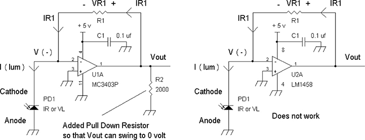
FIGURE 11.18 MC3403P (left side) and LM1458 (right side) photodiode preamps.
In Figure 11-18, the left circuit uses an MC3403P op amp that has an NPN-PNP push pull emitter follower output stage. Because the PNP output transistor’s emitter cannot deliver a voltage to 0 volts, there will be a problem with sensing small photocurrents. For example, if the photodiode current is 0 μA with R2 removed from the preamp circuit, and R1 = 100kΩ, Vout will be in the +50 mV to +200 mV range when measured with a DVM. To re-establish a truer linear relationship between light intensity and output voltage, pull-down resistor R2 is connected from pin 1 to ground. This ensures that the MC3403P’s output stage works as an NPN emitter follower capable of operating correctly all the way down to 0 volts. Typically, R2 can be a resistor in the range of 3300Ω to about 1000Ω. Thus, with R2 installed, when the photodiode current is 0 μA, Vout = 0 volt. Also note that the MC3403P’s input terminals will operate properly down to 0 volt.
The LM1458 circuit (right side) in Figure 11-18 will not work because the input circuit of an LM1458 or similar op amp cannot operate correctly when the (–) input terminal is at the same potential as its minus supply pin 4. The (–) input of an LM1458 or similar op amp requires at least 1.5 volts to 2 volts above the negative supply pin (e.g., pin 4).
A fix then is to replace the LM1458 op amp with op amps such as the TLC272 (16-volt max supply), MAX407 (10-volt max supply), NJU7002 (16-volt max supply) or CA3240 (32-volt max supply) whose input terminals can sense at ground and whose outputs can swing to ground.
Suppose we have the correct op amp in terms of input and output voltage ranges, can there be other problems? Yes, see Figure 11-19.
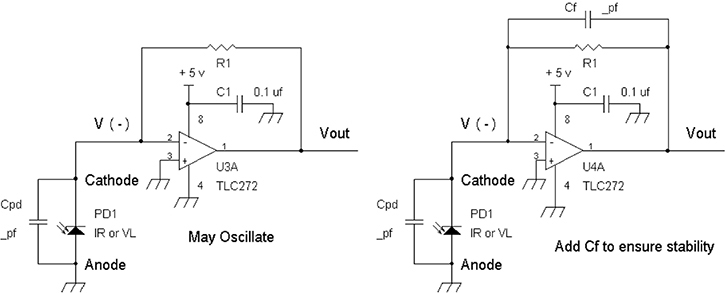
FIGURE 11.19 The photodiode’s internal capacitor, Cpd, can cause oscillations by added extra lagging phase shift in the feedback network via R1 and Cpd.
All semiconductors including diodes and transistors have internal capacitances across their terminals. In Figure 11-19 on the left side, the photodiode, PD1, has a built-in capacitor, Cpd. Typically, Cpd is in the range of 1 pf to as much as 100 pf, depending on the surface area of the photodiode. Since R1 typically has a value in the range of ≥ 100KΩ, the low-pass filter effect via R1 from Vout to V(–) with Cpd adds phase shift that can cause the circuit to oscillate.
For example, if you replace U3A with a faster op amp and or connect Vout to a capacitance load, it is possible to cause the op amp to oscillate. The oscillation frequency is generally > 1kHz such as 10kHz or more. To fix this problem, the circuit on the right side of Figure 11-19 shows a feedback capacitor, Cf, in parallel with R1. Cf with R1 forms a positive phase or leading phase network with respect to diode capacitance Cpd.
This positive phase or leading phase offsets/cancels the lagging phase caused by Cpd. At very high frequencies, the impedance of Cf is much smaller than the resistance of R1 such that we get a capacitive feedback network of Cf and Cpd. Since a capacitive voltage divider from Vout to V(–) does not exhibit phase shift, the circuit has less chance of oscillation. Generally, we choose Cf for minimum capacitance to maintain good high-frequency response or bandwidth. Typically, Cf is in the order of 1 pf to 10 pf. However, if we need to filter out noise while maintaining a lower but sufficient bandwidth, Cf can be increased.
The –3 dB frequency for bandwidth is: fc = 1/[2π (R1)(Cf)].
For example, if R1 = 1MΩ and Cf = 10 pf, then fc = 1/[2π (1MΩ)(10 pf)] or fc = 15.9 kHz. If you want twice the bandwidth, reduce the capacitance of Cf to half by setting Cf to 5 pf so that fc = 31.8 kHz.
We now turn to examples from the web (world wide web) or from some publications that show mistakes, but these circuits are easily remedied. Let’s start with Figure 11-20.
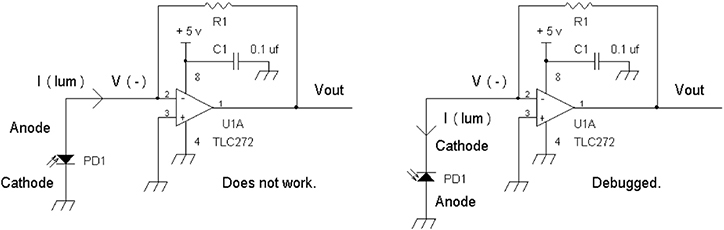
FIGURE 11.20 The left side circuit shows photodiode PD1 connected in reverse.
In one of the classes I taught concerning photo emitters and sensors, a basic single supply photodiode preamp was built. The output Vout seems to be stuck at 0 volts no matter how much light was shined into the photodiode. As can be seen in Figure 11-20’s left circuit, the photodiode’s anode is connected to the inverting input of U1A. Because the photocurrent positive current is flowing into the inverting input, we can expect to have a negative voltage at the output. This negative voltage output would be true if the negative supply pin 4 of U1 would be connected to a negative supply such as –5 volts DC. However, since pin 4 is grounded at 0 volts, this means the output voltage at pin 1 cannot go lower than 0 volts. Therefore, the output voltage is “clipped” at 0 volts. To fix this problem, just reverse the photodiode’s connections as shown in the right side circuit of Figure 11-20. This then has the photodiode current flowing out from the inverting input that provides a positive Vout. Also, note the op amp that was chosen allows the input terminals to operate correctly at ground, and that allows the output voltage to swing as low as ground. The output voltage for the right side circuit is Vout = I (lum) × R1. In Star Trek (TOS, the original series), the science officer usually saves the day by telling the chief engineer to invert phase. And this is one time it is correct to invert the phase of the photodiode to get the circuit working correctly. Now let’s look at Figure 11-21.
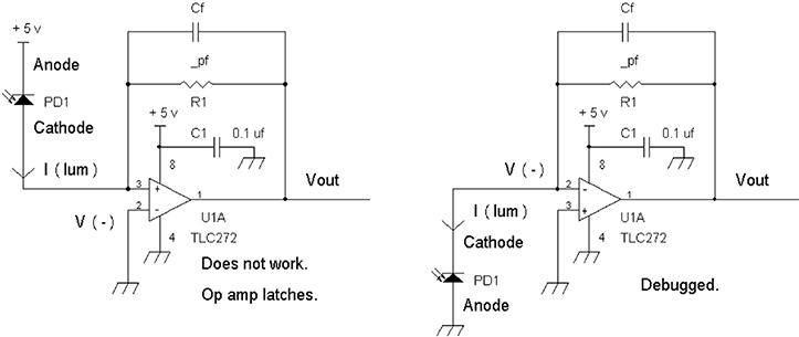
FIGURE 11.21 A example of inverting the phase of the photodiode and the inputs at pins 2 and 3 fixes the problems.
In this example, we have to invert phase twice. See the left circuit in Figure 11-21. And the mistakes we shall see are somewhat devoid of proper design.
For the left side circuit in Figure 11-21, the photodiode looks similar to the correct orientation for the photodiode’s current flow via I (lum); the configuration, however, is incorrect. Although the cathode of PD1 is properly biased to a positive +5 volts for reverse bias on the photo diode, there are two problems. First there is positive feedback via R1 via the (+) input being connected to the feedback resistor R1. When an op amp is connected in a positive feedback configuration like this, the concept of V(+) = V(–) at the input terminals does not apply. Generally, the op amp’s output signal at Vout may show oscillation or may latch to a DC voltage. With positive feedback it does not matter which way the photodiode is connected because the output signal will not be related to photodiode current. To fix the two problems, we have to first, reverse the input pins of the op amp and second, connect the photodiode as shown in the right side circuit of Figure11-21. Although the photodiode now sits at 0 volts DC bias, which is fine for most cases, there may be a reason for biasing the cathode of PD1 to a positive voltage. By applying a positive voltage that puts the photodiode into reverse bias, the internal photodiode capacitance reduces. We can take the anode of PD1 in the right circuit of Figure 11-21 and connect it to an available negative power supply. But suppose we only have the positive power supply. Can we still apply a positive reverse bias voltage to the cathode of PD1? The answer is yes. See Figure 11-22, which incorporates a second amplifier (e.g., you can use a dual op amp).
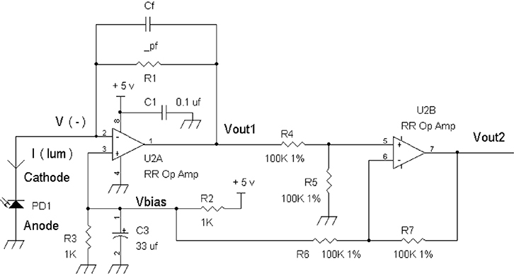
FIGURE 11.22 Biasing the photodiode’s cathode via Vbias and using a differential amplifier circuit via U2B. Note: RR Op Amp = Rail to Rail op amp such as an ISL28218.
We can set a positive voltage on the cathode of PD1 by having the (+) input of U2A biased with a voltage. In this case it is about one-half the supply voltage, or 2.5 volts in this case with a positive 5-volt power supply. Because we have a negative feedback circuit via R1 from Vout1 to the (–) input of U2A, the voltage at pin 2, V(–) is the same as Vbias. That is, under a negative feedback op amp circuit, the voltages at the input terminals are the “same.” Therefore with V(–) = Vbias, and Vbias = 2.5 volts, the cathode of PD1 is sitting at 2.5 volts DC.
The resistors R2 and R3 are chosen such that R2||R3 << R6. In general, we want R2||R3 ≤ 1% of R6. In this circuit, R2 = R3 = 1KΩ so R2||R3 = 500Ω and 500Ω is 0.5 percent of 100KΩ.
With R2 = R3, the current draw into R2 is (5 v)/(R2 + R3) or 5 v/2KΩ = 2.5 mA.
We can increase R2 and R3 to 2KΩ to save power if needed. Decoupling capacitor C3 with R2 and R3 forms a low-pass filter to reduce noise from the +5v supply line. The cut-off frequency of this low-pass filter is fc = 1/[2π(R2||R3)C3]. In this circuit we have:
fc = 1/[2π(1000Ω||1000Ω)33μf] = 1/[2π(500Ω)33μf] or fc = 9.65 Hz
And generally, we want fc << 60 Hz for good filtering. If needed, we can increase C3 from 33μf to 330 μf. A ≥ 10-volt capacitor should work fine since the supply voltage is +5 volts and with R2 and R3, nominally, there are only 2.5 volts across C3.
Vout1 is the summation of the bias voltage, Vbias and the photodiode current times R1 or Vout1 = Vbias + I (lum) × R1.
Essentially, this circuit is a voltage follower for Vbias since the photodiode, PD1, is a current source that has “infinite” DC resistance. So, there is no DC resistance value from cathode to anode of PD1. Again, see Figure 11-22.
The end game is to provide an output that is in the form of only I (lum) × R1, without any DC bias voltage. We then need to subtract out “exactly” Vbias from Vout1 = Vbias + I (lum) × R1. By using a differential amplifier U2B, the output of it is Vout2 = Vout1 – Vbias. Or put in another way (for the circuit in Figure 11-22), Vout2 = Vbias + I (lum) × R1 – Vbias = I (lum) × R1 = Vout2.
Differential amplifier U2B works as a unity gain subtractor when all four of the resistors, R4, R5, R6, and R7, are the same value. Note that they are 1 percent tolerance resistors.
Ideally, op amps U2A and U2B are from a dual package rail to rail (RR) output for maximum voltage swing such as NJU7062 or NJM2762. However, if you bias the cathode of PD1 to a slightly lower voltage such as 1.67 volts by having R2 = 2KΩ and R3 = 1KΩ, you can use other op amps such as TLC272 or CA3240 and still get good output voltage swing. Of course, if you just need a slight positive bias voltage at the photodiode cathode, such as a few hundred millivolts, you can set R2 = 10KΩ to have Vbias ~ +0.45 volts.
We now turn to a circuit found in a publication and on the web that is devoid of reliable operation. In a sense it is “bankrupt” in good electrical engineering practice.
(After all, this is Chapter 11 and we should cover at least one bankrupted circuit . . . just kidding!)
See Figure 11-23.
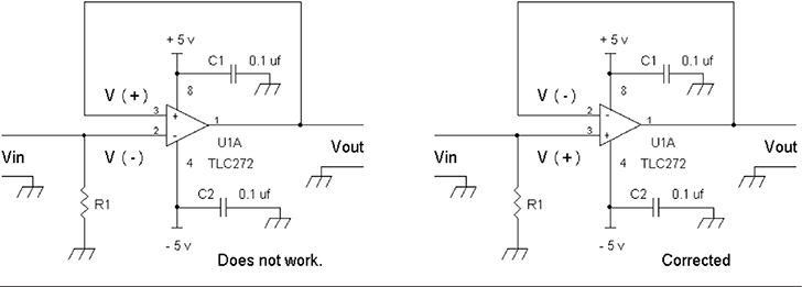
FIGURE 11.23 The left circuit is sometimes called an inverting voltage follower, which is incorrect.
In Figure 11-23, the left side circuit shows positive feedback because the output signal from Vout is connected back to the non-inverting input. This will cause the output signal to oscillate or latch to either a positive or negative voltage. With positive feedback we will find that the voltages measured at the non-inverting and inverting input terminals are not equal. That is, for the left circuit with positive feedback V(+) ≠ V(–).
To fix this circuit, you need to reverse the input leads as shown on the right side circuit of Figure 11-23. With this done we now have a standard unity gain non-inverting voltage follower where Vout = Vin, and V(+) = V(–).
Summary
In this chapter, we have been shown some examples of “bad” circuits, and there is a reason for showing these. As a hobbyist or even an engineer, oftentimes we assume what’s published in books or magazines or posted on the web (world wide web) is correct. In my experience, some of these non-working circuits have “typos,” others include misunderstandings of electronic principles such as the left side circuit in Figure 11-23, and yet other circuits that do not work can be attributed to an incorrect part or not knowing limitations of components (e.g., rail to rail op amps versus standard op amps). So, when we build such “bad” circuits exactly and check them over and over again and find nothing wrong construction-wise, it’s time to examine the circuit itself, and not assume that it actually works as advertised. As we get out of Chapter 11, which we did in a sense showing how to fix erroneous or “bankrupted” circuits, we will find even more types of these circuits ahead. Stay tuned to the next couple of chapters—more examples to come.
Reference Books
1. Arthur B. Williams, Electronic Filter Design Handbook, Second Edition. McGraw-Hill, 1988.
2. Paul R. Gray and Robert G. Meyer, Analysis and Design of Analog Integrated Circuits, Second Edition. Wiley, 1984.