CHAPTER 15
![]()
More Tips and Final Thoughts
We have looked at many types of analog circuits on the individual component level with resistors, capacitors, diodes, LEDs, transistors, and ICs.
However, when we troubleshoot circuits, sometimes we have to work from a schematic diagram that is not clearly drawn. In this chapter, we will present an example of how certain harder-to-read schematics are actually drawn today (2019) and how to fix them.
If you are stuck trying to figure out how to troubleshoot particular circuits such as high-fidelity amplifiers, radio circuits, etc., sometimes it is easier to download the service manual or schematics of similar circuits via the web and compare them with yours. For example, if you are troubleshooting a stereo power amplifier, you can go to websites such as:
• https://www.hifiengine.com/ Or you can pay a fee for schematics via SAMS Photofact.
• https://www.samswebsite.com/ If you have the manufacturer’s model number or chassis number, then you may find used copies via eBay. For example, if you have a Lafayette LR-4000 stereo receiver, you will find that that the SAMS Photofact booklet is “MHF-58,” for which you can do a search on the web.
The manufacturers’ service manual often includes DC bias point voltages, and some AC signal waveforms along with setup procedures.
There are other websites that post their schematics and service manuals and these can be used as a reference for troubleshooting. What you are doing is looking for products that should already work, and their circuits will generally reveal good engineering designs, but not always. The reason for looking at various commercial products’ schematics is to get a feel for how these circuits are designed well enough for repeatability.
I will also share with you how one “retro” circuit is driving analog meters the “wrong way” and the right way. Also, from many years ago, I will show how a circuit was fixed without fancy test equipment by looking for a similar schematic diagram.
Before I give my final thoughts, we will cover some basic problems due to bad connections on IC sockets and how to choose a better one for reliable operation.
Deciphering Schematics with Too Many Connection Flags
We will now look at a schematic example that is scattered and can be rearranged to show a clearer idea of what the circuit does. See Figure 15-1.
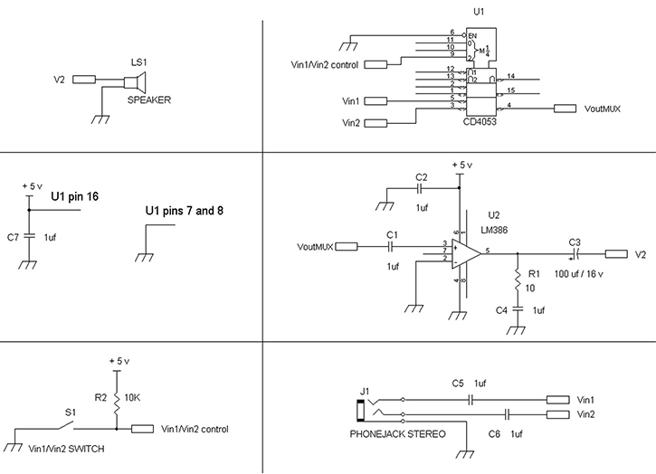
FIGURE 15.1 A “disjointed” schematic using net flags such as V2 from C3 connected to LS1.
We can start rearranging the schematic as shown in Figure 15-2 by connecting all the net flags and having the input on the left side and the output at the right side.

FIGURE 15.2 A rearranged schematic that is starting to make more sense, but does it work?
We can further improve the schematic by replacing U1 CD4053 with a better symbol.
Because U1 in Figure 15-2 looks more like a “black box,” we should find a schematic symbol that shows its operation. See Figure 15-3 that shows U1 having three analog switches.
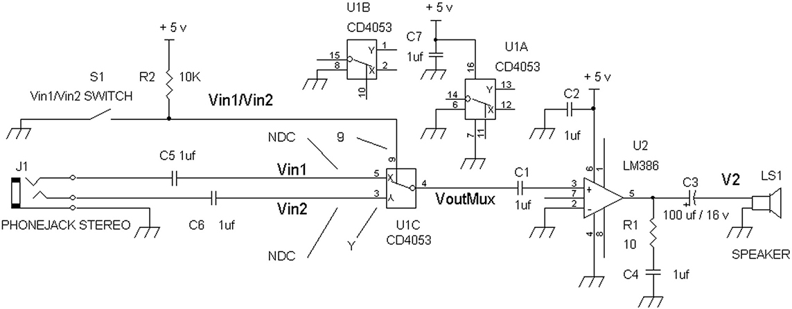
FIGURE 15.3 The CD4053 is revealed to be an X-Y two-channel analog switch that passes either an input signal from Vin1 or Vin2 via selector switch S1. Amplifier U2 LM386 then amplifies the selected input voltage for playing back on loudspeaker LS1.
From Figure 15-3 we see that the CD4053 switch is working off a single 15-volt supply due to its –VEE pin 7 being connected to ground instead of a negative supply. This means that the X and Y inputs at pins 5 and 3 should be biased to a DC voltage typically at one-half the DC supply voltage (e.g., 2.5 volts) for maximum AC signal swing. As shown in Figure 15-3, Vin1 and Vin2 are floating DC-wise and have no DC (labeled NDC) bias voltage.
As we can see by rearranging the schematic circuits from Figures 15-1 and 15-2 and inserting a more detailed circuit version of the CD4053, DC bias problems are found. We can now fix the circuit as shown in Figure 15-4 by adding a 2.5-volt biasing circuit.

FIGURE 15.4 Adding DC bias circuit R5, R6, and C8 provides 2.5 volts via R3 and R4 to the CD4053’s input pins 5 and 3 for Vin1 and Vin2.
In Figure 15-4, R5 and R6 form a voltage divider circuit that provides 2.5 volts into filter capacitor C8’s positive terminal. Capacitor C8’s capacitance is high so as to provide an AC short circuit to ground. This way, any AC voltage at R3 and R4 cannot cause crosstalk to each other. Without C8, some signals from Vin1 will “leak” over to Vin2 via R3 and R4. But with C8 as an AC ground we provide good isolation between the input signals Vin1 and Vin2. Capacitor C8 also reduces noise from the 15-volt power supply so that the output signal to the speaker is relatively noise free (e.g., no hum or no extraneous power supply noise).
Also note that there is a signal coupling capacitor C1 into U2 (LM386) pin 2 that does not seem to have a DC bias resistor. It turns out that the LM386 has an internal 50kΩ resistor from each of its input terminals (pin 3 and pin 2) to its ground pin 4.
When switch S1 is open circuit the Vin1/Vin2 control signal is logic high via +5 volts from R2 to control pin 9 of the CD4053, which selects the “Y” channel or Vin2. To select Vin1 or the “X” channel, S1 is closed, connecting R2 to ground. This (then) sends a logic low signal to control pin 9 of the CD4053.
Troubleshooting with Minimal Test Equipment
The next two sections will show methods that do not necessarily require any test equipment. Instead, we will use deductive reasoning or examples of circuits that are already commercially manufactured. The examples shown will be from my own experience before I worked in a TV/radio repair shop and also before I decided to study electronics formally. As a hobbyist back then, all I had were example circuits from other equipment.
Analog Meter Driving Circuits for AC Signals
This will be a story about learning how to drive analog meters correctly. See Figure 15-5.
FIGURE 15.5 An analog “VU” meter (Volume Unit audio meter) and a signal strength meter.
A circuit that works for sure to convert AC signals into DC currents is a full-wave rectifier. See Figure 15-6(a), which uses an AC coupling capacitor C1, where typically R1_meter ≥ 2000Ω to prevent burning out the analog meter, M1.
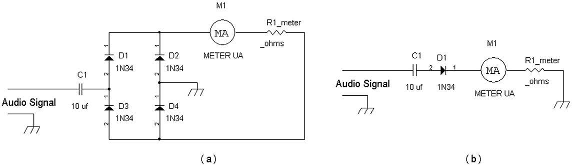
FIGURE 15.6 Full rectifier circuit that works (a) and one that does not work because of C1 (b).
With C1 the full-wave rectifier works well, and this circuit is used in many commercially made audio mixers such as the Shure M67. But what if you do not have four diodes for full-wave rectification as shown in Figure 15-6(a) and decide to use a half-wave rectifier circuit in Figure 15-6(b) instead? What you will find out is that the input capacitor C1 will block any DC current once it is charged up and the meter M1 will return to zero and will not operate as expected.
NOTE: Meter M1 is usually rated at 50 μA to 1000 μA full scale and R1_meter will be in the range of 2000Ω to 20kΩ. For example, the VU meter in Figure 15-5 (left side) has a full-scale reading at about 150 μA. Meter M1 has a 600Ω DC resistance, whereas the signal strength meter on the right side of Figure 15-5 has a 1200Ω DC resistance. Series resistor R1_meter prevents excessive current into meter M1.
CAUTION: Connecting a voltage source directly to meters usually results in burning them out. This is why a series resistor, R1_meter, is used to protect the meter, M1.
One idea we can “borrow” from power supply circuits is to use a transformer, which for sure produces a pulsating DC current with a half-wave rectifier. See Figure 15-7(a).
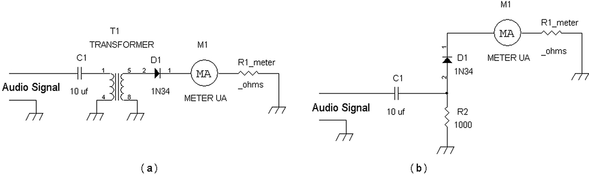
FIGURE 15.7 (a) Meter circuit now works by using a transformer; (b) an alternative using R2.
At the time the solution was in fact using an audio transformer such as a 10kΩ to 2kΩ primary to secondary impedance ratio transformer. In Figure 15-7(a), transformer T1’s primary winding at pins 1 and 4 allows for currents to flow in both directions through C1. Put in other words, AC currents are allowed to flow through C1 and T1’s primary winding. An AC signal voltage is then transferred to the secondary winding at pins 5 and 8, such that D1 rectifies the AC voltage at the secondary winding and provides a pulsating DC voltage to the M1 that then displays an average DC current set in part by series resistor R1_meter (e.g., 10kΩ).
In Figure 15-7(b) resistor R2 provides a DC path to ground and also allows currents to flow in both directions through C1. By simply adding R2, the meter circuit now works. This is a simpler solution given that resistors are more common than transformers.
Another circuit we can borrow from power supplies is the voltage doubler circuit. See Figure 15-8.
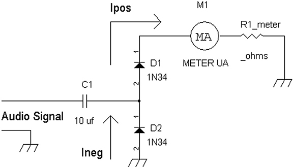
FIGURE 15.8 A voltage doubler circuit with additional diode D2 gives yet another circuit solution.
Diode D2 may be looked upon as a DC restoration circuit with C1, which means it level shifts the audio AC signal such that negative peak of the AC signal is “clamped” to about 0 volts or ground level. Diode D2 also provides a path for C1 to allow for signal flow in the negative direction (Ineg), while D1 allows C1 to flow currents in the positive direction (Ipos). At D1’s anode there is already a pulsating DC signal, and D1 ensures only positive going currents, Ipos, are sent to meter M1.
NOTE: The diodes used in most analog meter circuits are small signal germanium diodes such as 1N34, 1N60, 1N270, etc., to minimize forward diode drop losses (e.g., ≤ 200 mV). You can use small signal Schottky diode replacements such as BAT42, BAT43, BAT85, and BAT86 with ~ 300 mV turn-on voltage. Using standard diodes such as 1N914 or 1N4148 will have turn-on voltages in the 500 mV to 600 mV ranges, which means the meter circuit will require very large AC voltages greater than 5 volts peak to peak to have reasonable measurement accuracy. To avoid audio distortion caused by the meter circuit’s nonlinear load, a buffer amplifier can drive the meter circuit to isolate the main audio output signal path. Or instead, a near 0 Ω output resistance amplifier can drive a meter circuit and provide an audio output.
If you are wondering why the meter circuits are not directly connected to an op amp with positive and negative power supplies, then you have to consider start-up conditions and catastrophic failure modes. When an op amp is first powered on, there may be a large DC offset transient that may damage the meter. Having a DC blocking series capacitor (C1) ensures protection against long- or short-term DC voltages into the meter. Also, if a directly coupled amplifier such as an op amp fails, it may deliver a large sustained DC current into the meter that can cause damage.
Troubleshooting an Older Push Pull Audio Amplifier in a 1950s Transistor Radio
This is a story where the problem was solved over many years. The circuit was put aside because after replacing virtually every resistor and capacitor, there was still a problem. Since I did not have any more than an analog VOM and no schematics, I was not able to troubleshoot the problem. Also, I was just starting out in learning electronics at a time way before attending high school. See Figure 15-9.
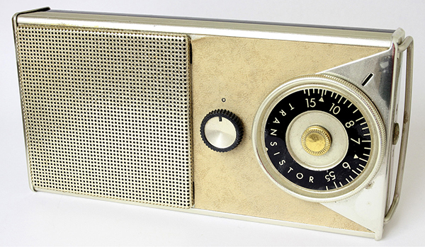
FIGURE 15.9 A General Electric model/chassis number P-716A six-transistor radio (year 1958).
The problem was the radio had a low volume and it sounded somewhat distorted.
JUST A REMINDER: I was just starting out in repairing radios like this and had no formal electronics background. And I only knew some basics like Ohm’s law but had no idea how to apply them because I had not taken algebra yet.
So how would one go about troubleshooting without much electronics resources? For example, I just had an analog VOM and no signal generator. At first, I “shot-gunned” it by replacing every resistor, capacitor, and transistor, but this did not help. It did not improve anything.
The way to signal trace the circuit is to hack another working transistor radio, which I had, to make it an audio signal tracer or speaker amplifier. I can then trace the audio signal at the General Electric P-716A’s volume control and subsequent audio stages. The audio via the makeshift audio signal tracer showed that the radio appeared to be fine up to the first audio transistor, but not at the speaker output.
So, I also traced out a partial schematic of the radio. Note that back in those days, there were no silkscreen reference designations for the electronic components. Also, these electronic parts such as resistors and capacitors were loaded with uneven spacing and at different non-standard angles (e.g., at 30 degrees, 45 degrees, etc.). Today’s printed circuit boards are usually loaded with parts at a reference zero degrees, such as East-West, or 90 degrees, such as North-South. Because the boards had a single layer of copper traces, components often had longer spreads to jump over traces beneath them. For example, the standard 400 mil (0.4 inch) spacing for quarter watt resistors may be extended to anywhere from 500 mils to 700 mils and mounted at an angle (referenced to either edge of the board). The type of component arrangement makes it hard to identify if all the components are put in their proper locations. See Figure 15-10. Note all audio transistors, Q1, Q2, and Q3 are germanium transistors.
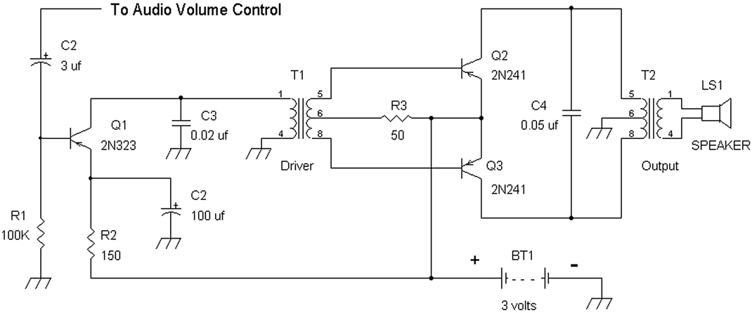
FIGURE 15.10 A partial traced-out circuit diagram of the GE transistor radio model P-715A, which uses two AA batteries to supply 3 volts.
If you are familiar with transistor amplifiers, you can spot the problem right away. But what if you lack the knowledge and need help because you think that the circuit in Figure 15-10 looks “reasonable” as a working audio amplifier? One way is to find a similar radio with a schematic diagram. See Figure 15-11.
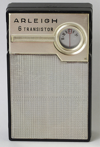
FIGURE 15.11 An “Arleigh” six-transistor radio that has a similar audio amplifier as the GE radio.
The Arleigh radio has a similar audio amplifier circuit so we can trace its circuit by taking it apart, or if there is a schematic available, we use that instead. Fortunately, there is a schematic diagram printed inside its back cover. See Figure 15-12.
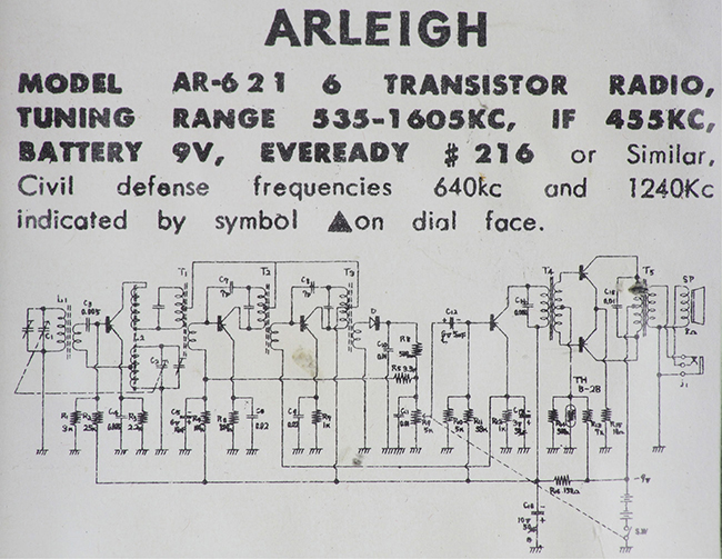
FIGURE 15.12 Arleigh radio’s complete schematic.
NOTE: There are biasing resistors (R13 and R14, which are not clearly seen here) connected to center tap of transformer T4 in Figure 15-12.
There is also a thermistor (temperature dependent resistor), TH B-2B, which is connected in parallel with R14.
For a closer look, see Figure 15-13, where extra notes have been added:
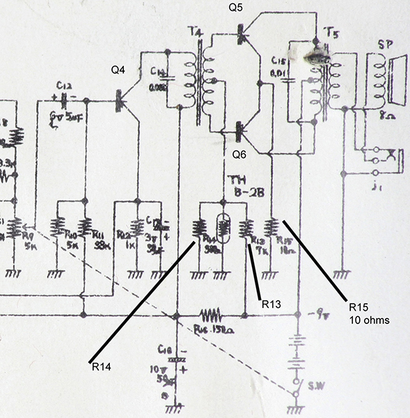
FIGURE 15.13 Biasing resistors R13 and R14 are connected to the center tap of driver stage transformer T4 of the Arleigh radio. The ground is connected to the plus terminal of the battery.
• The audio driver transistor is labeled as Q4, and the audio output transistors are labeled as Q5 and Q6.
• Resistors R13, R14, and R15 are identified. Resistor R15 = 10Ω, so essentially the emitters of output transistors Q5 and Q6 are connected to ground, or more importantly, they are connected to the plus terminal of the 9-volt battery.
If we just look at the connections to the 9-volt battery, its positive terminal is connected to ground via the on/off switch, S.W., and the battery’s negative terminal is connected to the lower side of R13 of Figure 15-13. The emitters Q5 and Q6 via R15 are essentially connected ground since R15 is 10Ω. This means the emitters of Q5 and Q6 are essentially connected to the positive terminal of the battery via S.W., connected to ground and the positive terminal of the battery. The lower side of resistor R14 is connected to ground, which means the lower side of R14 is also connected to the positive terminal of the 9-volt battery via S.W. In essence, R14 is connected across the center tap of T4 and “indirectly” connected to the emitters of the output transistors Q5 and Q6 (via the 10Ω resistor R15 in Figure 15-3).
We also have R13 at 7kΩ with one side connected to the negative terminal of the battery and its other side connected to the center tap of T4 and R14. If we look carefully, R13 with R14 and TH B-2B form a bias network for turning on Q5 and Q6. Thermistor TH B-2B is connected in parallel with R14.
This bias voltage across the emitter and base of Q5 and Q6 will be in the order of about 0.25 volts, which is the turn-on voltage of germanium transistors.
So, the mystery problem we had was that there was a part missing!
Now let’s look at the GE radio’s schematic again; this time we will add the missing biasing resistor. See Figure 15-14.
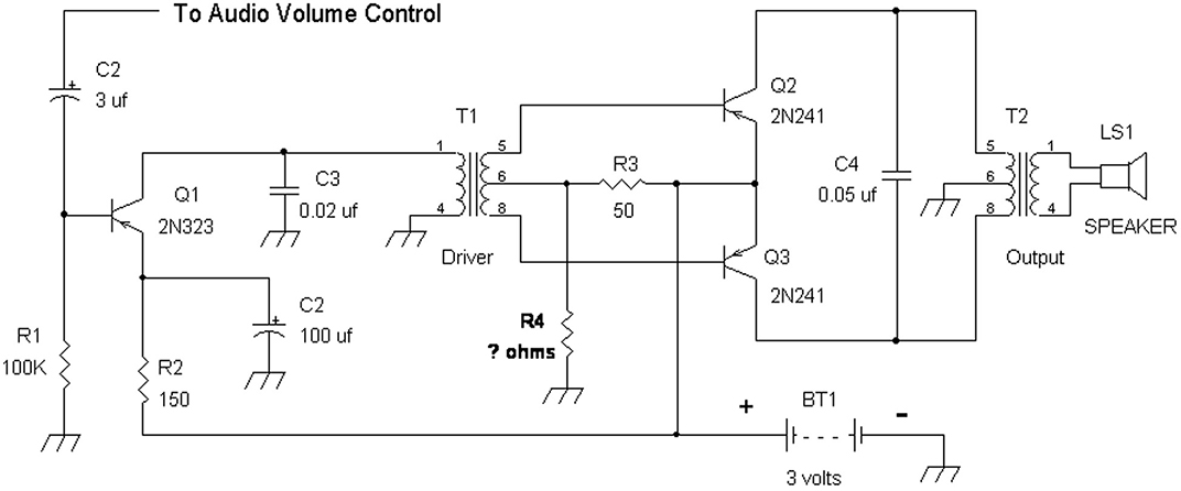
FIGURE 15.14 GE radio schematic with added resistor R4 (in bold fonts) connected to the center tap of T1 and to ground or equivalently to the negative battery terminal.
The R4 in the GE radio is sort of like the R13 (7kΩ) in the Arleigh radio. And R3 in the GE radio is like R14 and TH B-2B in the Arleigh radio. So, where do we start? Since the Arleigh radio uses 9 volts instead of the 3 volts in the GE P-715A, we can scale R13 down to about one-third of its value or R4. So R4 ~ R13/3 or 7kΩ/3 ~ 2333Ω ~ 2200Ω 5 R4.
With R4 ~ 2200 ohms the voltage across R3 (50Ω) in Figure 15-14 is: 3 volts 3 [R3/(R3 + R4)] or 3 volts 3 [50/2250] ~ 0.067 volt. We will get an improvement in sound with R4 = 2200Ω, but it is still not good enough. If we reduce R4 to 1000Ω, the voltage across R3 will be 3 volts 3 [50/1050] ~ 0.143 volt. This will be a dramatic improvement and could work out OK because germanium transistors have a turn-on voltage range between 0.10 volt and 0.3 volt.
Over 20 years later when I finally found the SAMS Photofact schematic for the GE P-715A radio, it clearly showed that the R4 value was 680Ω, which would yield across R3 a voltage of 3 × [50/(50 + 680)] ~ 0.206 volt.
So, yes, if I had found the schematic back then via SAMS Photofact, I would have solved the problem immediately. However, there will be times when the circuit diagram is not available and with limited resources (and sometimes limited electronics knowledge), we have to find other ways to troubleshoot the problem.
NOTE: Had I looked at the GE radio’s printed circuit board very carefully, I would have found two pads or two small holes that were there for a missing part.
Thus, one way is to learn from an example of a known working circuit. These days you can find example circuits by various manufacturers’ products via websites such as:
• http://www.nostalgiaair.org/Resources/ for old antique radios and television circuits
• http://bama.edebris.com/manuals/ for almost everything related to test equipment, HiFi products, etc.
• https://www.vintage-radio.info/heathkit for Heathkit schematics and manuals
• https://www.vintageshifi.com/repertoire-pdf/Dynaco.php for Dynaco HiFi stereo products (preamps, power amps, and tuners)
Also, you may find specific schematics posted on the web by using Google. For example, if you need to know product or model numbers of certain products, you can look through archives of older electronics or stereo magazines such as: https://www.americanradiohistory.com/High-Fidelity-Magazine.htm for High Fidelity Magazine or https://www.americanradiohistory.com/Audio-Magazine.htm for Audio Magazine. Once you have the manufacturer’s model number, you can look up a service manual or schematic from https://www.hifiengine.com/.
Reducing Noise on the Power Supply Bus with Multiple Circuits
When a large system having multiple circuits is supplied with a common power supply voltage, each circuit can generate noise back into the common power supply bus or line. See Figure 15-15. In the ideal world VCC = VCC1 = VCC2 = VCC3, but this does not really happen.
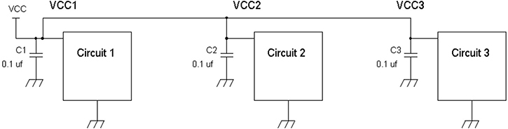
FIGURE 15.15 A common VCC voltage supplying three circuits where the drain from each circuit can generate its own noise at its supply node, VCC1, VCC2, and VCC3.
While in the ideal world, VCC supplying all three circuits would have no noise, each circuit can contribute to its own noise due to AC signals running in Circuit 1, Circuit 2, and or Circuit 3. For example, if Circuit 1 is an oscillator circuit, and Circuit 2 is a microprocessor circuit, and Circuit 3 is a memory circuit, each circuit will be turned on and off in such a way to cause transient noise spikes that may be at different times. These noise voltage transients along the power supply lines mean that VCC1 ≠ VCC2 ≠ VCC3 at different times. If the noise transient spikes are large enough, they can interfere with proper signal processing for each circuit. One solution is to isolate the noise transient spikes and improve power supply decoupling for each circuit. See Figure 15-16 where the circuits are isolated with inductors L1 and L2.

FIGURE 15.16 Circuits 1 to 3 have series inductors forming a pi filter (π filter) with C2/CB, L2 and C3/CC and another with C1/CA, L1 and C2/CB.
A pi filter refers to an analogous mechanical construction having two “pillars” supporting a horizontal bar that is denoted by π. The capacitors form the pillars and an inductor forms the bar.
In Figure 15-16, typical inductance values for L1 and L2 range from 1 μH to 100 μH. Note that added capacitors CA, CB, and CC are lower in capacitance at 1000 pf (1 nf) for better decoupling at higher frequencies such as ≥ 50 MHz. If the circuits are running in the GHz range, the decouple capacitors have to be reduced in value accordingly, such as CA, CB, and CB = 220 pf for power supply decoupling. The reason is that at higher frequencies virtually every capacitor includes a (significant) series inductor. That series inductor decreases with smaller capacitance values, which allows the capacitor to effectively remove high-frequency noise at the power bus. For example, if your circuit is running at 100 MHz, using a 0.1 μf to 1 μf capacitor does almost nothing in terms of acting like an AC short circuit at that frequency. The reason is because 0.1 μf or more has a relatively large series inductor that negates a low impedance across the capacitor at 100 MHz. However, a 1000 pf capacitor has a much smaller series inductance and will be effective in acting like an AC short circuit at 100 MHz.
Figure 15-17 shows another example of isolating noise from the power bus (e.g., VCC).
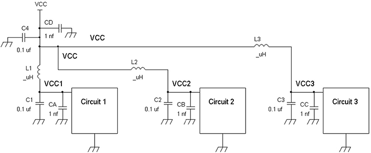
FIGURE 15.17 The common supply voltage VCC is spread out via inductors L1, L2, and L3.
In Figure 15-17, if there is noise at VCC1, VCC2, and or VCC3, each noise component will be filtered or attenuated at VCC via inductors L1, L2, and L3. Any noise at VCC then gets filtered again via L1/C1/CA, L2/C2/CB, and L3/C3/CC. This arrangement requires more components to be added but can be very effective in ensuring power supply noise from one circuit (e.g., Circuit 1 or Circuit 2 or Circuit 3) does not “contaminate” the supply voltages of the other circuits.
In general, for Figure 15-16 or Figure 15-17, each of Circuit 1, Circuit 2, Circuit 3, and so on can include a single stage amplifier such as an IF (intermediate frequency) amplifier, RF (radio frequency) amplifier, and or logic gate/circuit. The inductors L1, L2 . . . may be replaced with ferrite bead inductors. If the current draw of each circuit is not too high, such as < 10 mA, the inductors may be substituted with a 10Ω to 22Ω resistor, but the isolation characteristics in terms of power supply noises between the circuits may not be as high when compared to using inductors (e.g., L1, L2, and L3).
Bad Connections from Some IC Sockets
Whenever you purchase IC sockets, especially the ones that are “all plastic,” there may be a chance that they may not make good contact or electrical continuity with the IC’s pins. And if the integrated circuit itself has slightly oxidized pins, some sockets may cause an open circuit between the pins of the IC and the IC socket terminals. See Figure 15-18.
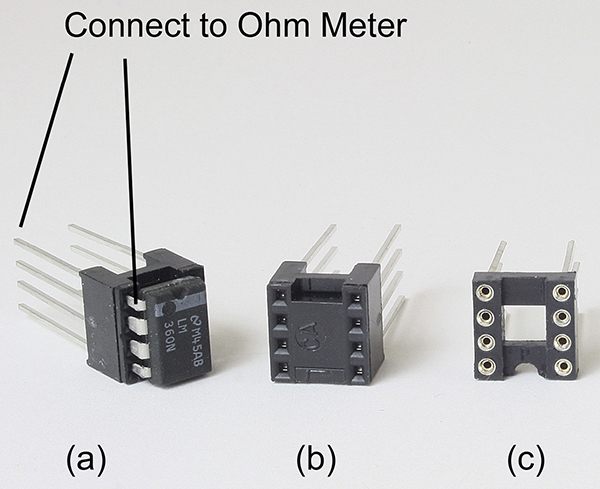
FIGURE 15.18 Full plastic sockets shown in (a) and (b), with a socket with round pins for better reliability shown in (c).
An IC is installed on a “fully” plastic socket in Figure 15-18(a). These types of sockets are generally fine but can have continuity problems. To be sure, use an ohm meter to measure each pin of the IC with its corresponding IC terminal lead. Figure 15-18(a) shows an example of how to measure pin 1 of the 8-pin IC, but you will have to go through every pin for a continuity check via an ohm meter.
Next, Figure 15-18(b) shows the unloaded plastic socket. Sometimes if you have already soldered this type of socket and found a continuity problem, one way to resolve the issue to remove the IC from the socket (e.g., via a small flat blade screwdriver or with an IC pulling tool) and then reinsert the IC back into the socket. By doing this, you may have “cleaned” the connections.
If you want higher reliability, you can use a socket with round pins as shown in Figure 15-18(c). The round “wells” allow self-cleaning of the IC’s pins by wiping against the edges of the IC pins to ensure better connections.
Summary and Final Thoughts
We’ve seen that troubleshooting circuits includes the following:
• A knowledge base of components and how to use them properly. This includes operating them below their maximum voltages/currents/power ratings (e.g., capacitors, transistors, resistors, logic circuits/gates, etc.) and connecting them with the correct polarity (e.g., electrolytic capacitors, LEDs, transistors, ICs, etc.).
• Using your volt meter to confirm the DC voltage operating points in your circuits and power supplies are at the correct voltage.
• Using your ohm meter to measure resistors with the circuit power shut off and with at least one lead of the resistor disconnected.
• You can buy DVMs to measure capacitors, which is very important since many capacitors have the same size but very different capacitances (e.g., 10 pf to 1 μf). Thus, it can be easy to install the wrong valued capacitors. Also, if you are working with surface mount capacitors, they may not be marked, so a capacitance meter comes in handy.
• Most DVMs will also allow you to check NPN and PNP transistors and diodes. This is very useful since the pin outs to transistors are not the same such as a 2N3904 (emitter, base, collector) versus a BC550 (collector, base, emitter), or an ultra-high-frequency transistor 2SA1161 (base, emitter, collector).
• Look up specifications for your parts and download a “library” of data sheets. This includes transistors, ICs, and diodes. Keep the data sheets handy for reference. For example, if we look for low–drop-out (LDO) voltage regulators, then we will see that there can be two different types. There is one with a typical drop-out voltage ~ 0.5 volt (e.g., adjustable voltage LM2941 or fixed voltage LM2940) that will have a PNP output transistor’s collector connected to the output of the regulator. However, there is another one with higher drop-out voltage of ~ 1.0 volt to 1.2 volts (e.g., adjustable voltage LM1117), where the emitter of the NPN output transistor is connected to the output terminal. Note that the LM317 with a Darlington emitter follower output circuit is a standard adjustable voltage regulator, and it has a typical drop-out voltage of about 1.8 volts. Studying data sheets is a must if you want to ensure the circuits are using the correct electronic components.
• If you are using power supplies, always turn the settings to 0 volts for each output before connecting to your circuit because the supply may have been already set to an excessively high voltage that will damage your transistors or ICs. Set the voltage first, confirm with a DVM, confirm the polarity, and then connect the power supply leads to your circuit. If the power supply has a current limit feature, set it at about 100 mA unless you know your circuit drains more than that, which means you can increase the current limit.
• When using positive and negative supply voltages, you can need to connect a common lead such as the (–) lead of the positive voltage source to the (+) lead of the negative supply. Then this common lead will be used as the ground connection to your circuit.
• Have a kit of spare parts such as resistors, capacitors, transistors, diodes, etc. Sometimes it is just easier to replace a component to see if the circuit is fixed. For example, in discrete audio power amplifiers, you start with replacing the output transistors since they are usually the first ones to blow out. Also, in some cases with RF circuits, having spare crystals is a must. Crystals can stop working, or some of them could have been damaged due to excessive AC signal voltages across them. For example, some two-way radios have crystal oscillators where the crystals fail in about 10 or 20 years.
We have presented troubleshooting techniques for various circuits, including some not exactly well-designed circuits that were posted on the web or published. In many cases, troubleshooting is about detective work. This includes gathering data via specification sheets, schematics of similar circuits, using your basic test equipment such as a DVM or signal generator, and confirming the correct operation of the electronic components (e.g., an op amp used as an amplifier should have approximately 0 volts across its (+) and (–) input terminals). By process of elimination you can pinpoint the problem. For example, you can start probing for an output signal and work back to the input circuits.
As with any skill, troubleshooting circuits requires experience. The more circuits you are able to fix, the better you will be able to utilize your institutional knowledge for solving future problems. So even if you are not repairing a circuit at the moment, a good way to build up your electronics knowledge is to just read and study lots of schematics of manufactured products. These are readily available on the web these days.
If you are designing circuits or putting together sub-circuits, then whenever possible build a breadboard before you commit to a printed circuit board design. The reason for this is that not all circuits will “talk” to others flawlessly. By building a prototype first, you get to see just how well each circuit behaves under non-ideal conditions, such as with noisy power supplies or with a range of supply voltages. For example, does the circuit still work under worst-case conditions such as a specified low supply voltage or under maximum voltage input to the circuit?
Another item to look out for is to avoid the trap of KISS (Keep It Simple, Stupid) by trying to design your first circuit with minimum components count. You should look at the big picture and try to get the design to work first. Then, if possible, see if the parts count can be reduced without sacrificing performance and reliability. Some of my colleagues went by the KISS philosophy and found that their designs were lacking in performance and reliability. This caused them to cut traces and/or add piggy-back boards to their printed circuit boards. If they had just added a few more components in the first place, all this would have been avoided.
If you are designing circuits based on application notes, it’s best to also breadboard these circuits. By doing this you will find out what works in terms of laying out the components and of the best wiring routes that will ensure a less noisy circuit. For example, some signal traces may have to be shielded via one or more ground planes on the board. Also, you may find that not all power supply decoupling capacitors work equally. For example, some ceramic capacitors may be too lossy or have poor capacitance tolerance due to working DC voltage limit and temperature. Again, for example, a 1-μf ceramic capacitor rated at 90 percent of its DC working voltage may only deliver about 50 percent of its specified capacitance such as 0.47 μf. In some circuits, such as active filters using op amps, 2 percent tolerance film capacitors and 1 percent metal film capacitors may be a better choice of components than using 10 percent ceramic capacitors and 5 percent resistors.
On another note, there are some DC-to-DC converter circuits that will input 15 volts from your USB port and provide one or more output voltages, such as +12 volts, +12 volts and –12 volts, +3.3 volts, etc. Generally, these DC-to-DC converters will have high-frequency ripple noise at their outputs, and may radiate high-frequency noise via associated inductors. You may need to follow each output with a linear regulator (e.g., low–drop-out [LDO] adjustable voltage regulator), or add some series inductor-capacitor low-pass filters. For example, add a 1000-μH series inductor with a 1-μf shunt capacitor, such as L3 and C3 shown in Figure 15-17. Definitely if you are working with preamplifier circuits, make sure you do not directly connect a switching supply’s voltage to a microphone or photo diode bias circuit. For an electret microphone bias circuit, add a low-pass filter such as a 220Ω resistor in series with the switching supply that is followed by a 470-μf shunt electrolytic capacitor and be mindful of polarity (e.g., if you are using a positive supply, the negative lead of the electrolytic capacitor is grounded). If you are biasing a photodiode such as supplying a negative voltage to the anode lead, then you can connect a 2200Ω resistor between the negative switching supply and the anode of the photodiode. Then connect a 1-μf to 10-μf ceramic capacitor to the photodiode’s anode lead and ground the other lead of the ceramic capacitor to form a low-pass filter (that will reduce power supply noise).
So, these are my final thoughts, and good luck with troubleshooting circuits!
(Also following this chapter, be sure to check out Appendix A on test equipment.) See below for a preview on test equipment. Figure 15-19 shows a tester.
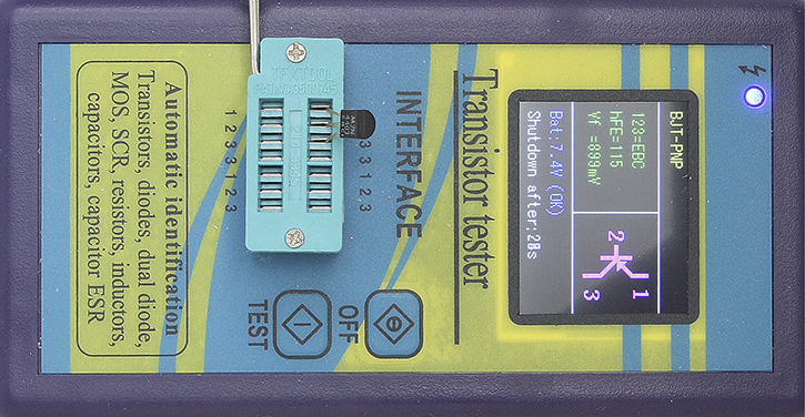
FIGURE 15.19 A component tester that not only tests various devices (transistors, FETs, diodes, capacitors, inductors, and resistors), but it also identifies the pin outs and polarity of the device. As shown above, the device is a PNP transistor with EBC pin out.