
Chapter 4. Fabrication technologies
Chapter Outline
4.1. Silicon-Based Microtechnologies114
4.2. Polymeric Microtechnologies132
4.3. Metallic Microtechnologies150
4.4. Packaging153
4.5. Conclusions155
References156
Micromixers can be fabricated using microtechnologies that were previously developed for microelectromechanical systems (MEMSs). Microdevices have feature sizes ranging from 1μm to 1mm. In most cases, these devices are fabricated in a batch process with techniques such as photolithography or imprinting. In the early development stage, most of these devices were fabricated based on established technologies from microelectronics, where thousands of devices can be fabricated on a single silicon wafer. Miniaturization increases the functionality significantly and decreases the fabrication cost. Micromixers can benefit from increasing functionality through the integration of electronic, mechanical, optical, fluidic, and other technologies in a single device. This functionality may lead to new applications, especially in life sciences.
Micromixers can be fabricated using microtechnologies that were previously developed for microelectromechanical systems (MEMSs). Microdevices have feature sizes ranging from 1μm to 1mm. In most cases, these devices are fabricated in a batch process with techniques such as photolithography or imprinting. In the early development stage, most of these devices were fabricated based on established technologies from microelectronics where thousands of devices can be fabricated on a single silicon wafer. Miniaturization increases the functionality significantly and decreases the fabrication cost. Micromixers can benefit from increasing functionality through the integration of electronic, mechanical, optical, fluidic, and other technologies in a single device. This functionality may lead to new applications, especially in life sciences.
Micromixer is one of the many micromachined devices that were reported in the past. With almost 30 years of development, micromachined devices are numerous and cover a wide range of applications. While in the 1980s and early 1990s, the development of microdevices was focused on physical sensors such as pressure sensor, accelerometer, and gyroscope, recent development points to research areas such as radio frequency (RF) MEMS, optical MEMS, and BioMEMS for biochemical and chemical applications [1]. Most of the microdevices in the past were fabricated either in single-crystalline silicon with bulk micromachining or in polycrystalline silicon using surface micromachining. Silicon has the advantages of established technologies coming from the decades-long development of microelectronics. However, silicon has poor mechanical and tribological properties, cannot withstand extremely high operation temperature, and, in some cases, is not biocompatible as well as chemically compatible. The need of other materials with properties suitable for applications in the chemical industry or life sciences leads to the development of microtechnologies based on other materials, such as diamond thin film, silicon carbide, polymer, and metals.
4.1. Silicon-Based Microtechnologies
The history of silicon-based micromachining dates back to the 1960s, when thin silicon membrane was etched to make pressure sensors. Bulk micromachining subsequently has been used for making inkjet print heads, accelerometers, gyroscopes, and other sensors as well as actuators. Based on CMOS (complementary metal-oxide-semiconductor) technology, freestanding polysilicon structures were fabricated by etching a sacrificial layer. This technique laid the foundation for the so-called silicon surface micromachining technology, which was widely adopted in the industry for making accelerometers, gyroscope, and comb-drive actuators. The most famous applications of surface micromachining technologies are accelerometers made by analog devices and digital mirror display made by Texas Instruments.
4.1.1. Basic technologies
4.1.1.1. Photolithography
The batch fabrication for the majority of microdevices is based on photolithography, a technology adapted from microelectronics. The different lithography techniques include photolithography, electron lithography, X-ray lithography, and ion lithography [2], of which photolithography and X-ray lithography for LIGA1 are the most relevant techniques for the fabrication of micromixers. Since photolithography requires a mask to transfer patterns to a substrate, this technique and almost all other microtechniques are limited to the fabrication of two-dimensional structures. There is little control over the third dimension. The pattern of microstructures is transferred through the mask to a photosensitive emulsion layer called photoresist. The mask is a transparent glass plate. The patterns are made of a metal layer, such as chromium, to block light. A mask printed on a plastic transparency film by high-resolution laser printer is popular in the microfluidics community due to its low cost and fast prototyping. The relatively large size of microfluidic components, such as micromixers, allows the use of this low-cost mask.
The photolithography process consists of three basic steps: positioning, exposure, and development. In the first step, the mask is positioned laterally to a substrate, such as a silicon wafer. The substrate is coated with a resist, which will carry the pattern after the subsequent exposure step. After lateral positioning, the distance between the mask and substrate is adjusted. The exposure step transfers the pattern on the mask into the photoresist layer. Energy from the exposure source, such as ultraviolet (UV) light or X-ray, changes the properties of exposed photoresist. In the development step, unexposed negative resist is dissolved, while the exposed area remains due to crosslinking. In contrast, exposed positive resist is etched away in the developer solution.
According to the relative position between the mask and the photoresist layer, photolithography is categorized as contact printing, proximity printing, and projection printing. In contact printing and proximity printing, the mask is brought close to the substrate. The resolution b of proximity printing is determined by the wavelength λ and the distance s between the mask and the photoresist layer [2]:
(4.1)
The resolution of a projection printing system can estimated as
(4.2)
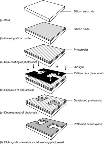
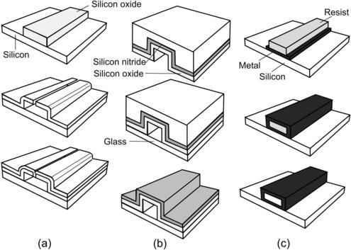
Because of its simplicity and fast prototyping process, photolithography of thick resists is a favored technology for the fabrication of micromixers. Thick resists structured by photolithography can be used as a template for molding polymeric devices or for electroplating of metallic parts. For the molding application, the resist structure should have high aspect ratio, which is suitable for making microchannels. The high aspect ratio requires special resists, such as SU-8 or high-energy beam (e.g., X-ray). If conventional UV source is used for the exposure, a thick-resist layer may degrade the resolution because the best depth of focus offered by proximity printing is only on the order of 5μm. For a simple estimation, the resolution is approximately one-third of the resist thickness. Figure 4.1 shows the typical steps for patterning a silicon oxide layer on a silicon substrate using photolithography.
4.1.1.2. Chemical vapor deposition
The patterns transferred from the glass mask to the photoresist are often further copied to a functional layer by etching. The functional layer is deposited before applying the photoresist. Chemical vapor deposition (CVD) is one of the many techniques for creating material films on a substrate. CVD utilizes chemical reaction between gaseous reactants to form a single solid product. The solid product is formed as a thin film on a heated substrate surface. The other reaction products should be in the gaseous form so that they can leave the reaction chamber. CVD processes are categorized based on reaction conditions. The common processes are atmospheric-pressure chemical vapor deposition (APCVD), low-pressure chemical vapor deposition (LPCVD), and plasma-enhanced chemical vapor deposition (PECVD).
APCVD and LPCVD processes require relatively high temperatures ranging from 500°C to 800°C. The high process temperature causes metals with low eutectic temperature with silicon, such as gold (380°C) or aluminum (577°C), to melt. Thus, metals with high eutectic temperature, such as tungsten, are suitable for deposition before APCVD or LPCVD processes. The alternative for a low-temperature substrate material is PECVD, which only requires temperatures typically on the order of 100–300°C. Table 4.1 lists common chemical reactions used in CVD of different material films and their corresponding process parameters.
| Material | Chemical Reactions |
|---|---|
| Silicon | SiH4→Si+2H2 ↑ |
| SiH2Cl2→SiCl2+2H2 ↑ | |
| SiCl2+H2→Si+2HCl ↑ | |
| Polysilicon | |
| Silicon dioxide | |
| Silicon nitride | |
| Silicide | |
4.1.1.3. Thermal oxidation
Silicon dioxide can be deposited with CVD if the substrate is a material other than silicon. If the substrate is silicon, thermal oxidation is the simplest technique to create a silicon dioxide layer. Based on the type of oxidizer, thermal oxidation is categorized as dry oxidation or wet oxidation. Dry oxidation utilizes pure oxygen to form silicon oxide at high temperatures from about 800°C to 1,200°C:
(4.3)
The oxidant in wet oxidation is water vapor:
(4.4)
4.1.1.4. Physical vapor deposition
In contrast to CVD and thermal oxidation, physical vapor deposition (PVD) creates material films on a substrate directly from a solid source. PVD is suitable for the deposition of electrically conducting layers such as metals or silicides. The technique covers two physically different methods: evaporation and sputtering.
Evaporation deposits a thin film on a substrate by sublimation of a heated source material in a vacuum. According to the different heating techniques, evaporation can be categorized as vacuum thermal evaporation (VTA), electron beam evaporation (EBE), molecular beam epitaxy (MBE), or reactive evaporation (RE). The first two methods are the most common. Resistive heating, laser heating, or magnetic induction is used in VTA. EBE utilizes an electron beam focusing on the target. Alloys can be deposited with evaporation using two or more material sources. However, sputtering is more stable than evaporation in the case of alloy deposition.
Sputtering utilizes a strong electromagnetic field to ionize a chemically inert gas, such as argon, and makes it become a plasma. The positively charged argon atoms are accelerated and bombard the target material. The bombardment knocks out target atoms, which are then condensed on the substrate surface as a thin film. Sputtering can deposit all types of materials, such as alloys, insulators, or piezoelectric ceramics. Sputtering is less directional than EBE but has higher deposition rates.
4.1.1.5. Spin coating
Spin coating is the simplest method for fabricating a film on a substrate. Thin-resist layers for photolithography are coated with this technique. The spin-coating process starts with the dilution of the material to be deposited in a solvent. The solution is subsequently dispensed on the substrate surface. The wafer is then spun at a high speed. The thickness of the film is determined by the spinning speed, surface tension, and viscosity of the solution. The solvent is removed partly during the spinning process due to evaporation and partly by subsequent baking at elevated temperatures. Spin coating results in a relatively planar surface. This technique is often used for planarization purposes. Spin coating can be used for the deposition of sol-gels. In this process, solid particles of a polymer compound dissolved in a solvent are spin-coated on the substrate surface. The process forms a gelatinous network on the substrate surface. Subsequent removal of the solvent solidifies the gel, resulting in a solid film. This technique can be used for the deposition of various ceramics, such as lead zirconate titanate (PZT). Besides spin coating, dry lamination, dip coating, spray coating, and electrodeposition can be used for transferring a resist layer to the substrate surface.
4.1.2. Single-crystalline silicon
Because micromachining technologies have emerged from microelectronics, silicon remains as the most important electrical and mechanical material for microsystems and microfluidics. The technology is established, and single-crystalline silicon wafers with high purity are commercially available at a relatively low cost. In the early development, most micromixers were fabricated in silicon. In general, silicon-based technologies are categorized as bulk silicon micromachining and silicon surface micromachining. Bulk micromachining utilizes the single-crystalline silicon substrate as the device material. Microchannels are etched directly into the silicon substrate. Surface micromachining can utilize both single-crystalline and polycrystalline silicon as device materials. The single-crystalline silicon wafer only acts as a carrier. Surface micromachining based on single-crystalline silicon is also called epi-micromachining or near-surface micromachining.
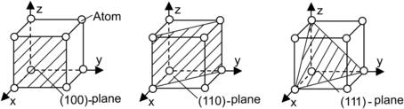
Single-crystalline silicon wafers are classified by the crystalline orientation of their surfaces. The classification is based on the Miller indices, which are shown in Fig. 4.2. A direction is described with square brackets, such as [100]. Because of the symmetry, there are a number of [100]-directions. A set of equivalent directions is described with angle brackets, such as <100>. If this direction is the normal vector of a plane, the plane is denoted with parentheses such as (100). The set of equivalent planes is described with braces, such as {100}. Single-crystalline silicon is mostly fabricated with the Czocharalski method (CZ method). This method starts with a small seed crystal, which determines the orientation of the silicon substrate. The seed crystal is dipped into a highly purified silicon melt and slowly pulled out of the melt, while the crucible containing the melt is rotated. Silicon crystals are grown along the selected orientation of the seed to a rod. Floating zone method (FZ-method) is the other method for fabricating silicon crystals. Instead of a silicon melt, a polysilicon rod is used as the starting material. A seed crystal at the end of the rod defines the orientation. The polysilicon rod is locally melted by radio-frequency heating. Crystal growth starts from the end with the seed. Following the crystal growth process, the silicon rod is then sawed and polished into wafers.
4.1.2.1. Wet etching
Wet etching is referred to as an etching process of solid materials in a chemical solution. During these processes, the substrate is dipped in the solution or the solution is sprayed on the substrate. Wet-etching processes are mostly isotropic, independent of crystalline orientation. However, as discussed later in this section, etching of single-crystalline silicon in KOH depends on the crystalline orientation. For the fabrication of micromixers, wet etching is often used for making the microchannel network.
Isotropic etching has drawbacks in fabrication of precise lateral structures because of underetching. If the etch solution is well stirred, the isotropic etch front has almost a spherical form. If a microchannel is fabricated with isotropic etching, the channel width also depends on the channel depth and needs to be considered in the mask design. The major advantages of wet etching include the high selectivity, a relatively planar etching surface, a high repeatability, and the controllable etch rate. Isotropic wet etching is often used for removing thin layers or thinning a film. Due to possible bubble formation on the etched front, well-stirred etch solution is crucial for the process quality. Isotropic wet etching of silicon can be achieved using a mixture of acids such as hydrofluoric HF and nitric acids HNO3. The etching process consists of two steps: oxidation of silicon by nitric acids and dissolution of formed silicon oxide by hydrofluoric. The disadvantage of isotropic etching is its controllability; very small structures cannot be fabricated by this technique. Table 4.2 lists some common recipes for isotropic wet etching.
| Material | Etchants | Selective To |
|---|---|---|
| Si | HF, HNO3, CH3COOH | SiO2 |
| Si | KOH | SiO2 |
| SiO2 | NH4, HF | Si |
| SiO2 | HF, NHO3, H2O | Si |
| SiO2 | H3PO4, NHO3, H2O | Si |
| Si3N4 | H3PO4 | SiO2 |
| Al | H3PO4, HNO3, H2O | SiO2 |
Anisotropic etching of silicon is usually achieved with KOH. The etch rate of KOH in single-crystalline silicon depends on the crystalline orientation. The (111) plane of the silicon crystal has two orders of magnitude slower etch rate than the (100) plane; so, single-crystalline structures etched in KOH are defined by the (111) plane. Because of this, the etching process in KOH is also called anisotropic etching. Since this technology is a wet-etching process, the equipment is simple and easy to implement. Because KOH is a source of mobile ion contamination, anisotropic etching in KOH is not compatible with standard CMOS processes. The problem of metal ions can be avoided by using a barrier layer or a metal-ion free etchant such as TMAH. While the standard CMOS process allows the fabrication of a number of microsensors, more complex devices can be fabricated by the combination between the standard CMOS process and an additional micromachining process. The additional process can precede (pre-CMOS), follow (post-CMOS), or be between the steps (intermediate-CMOS) of the standard CMOS process.
In an anisotropic wet-etching process, hydroxides react with silicon in the following steps [7]:
(4.5)
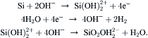
The overall reaction is
(4.6)
• Alkali hydroxide etchants – KOH, NaOH, CsOH, RbOH, or LiOH;
• Ammonium hydroxide etchants – ammonium hydroxide NH4OH, tetramethyl ammonium hydroxide (TMAH) (CH3)4NOH;
• Ethylene diamine pyrochatechol (EDP, which is hazardous and causes cancer, and should be accompanied by safety measures) – a mixture of ethylenediamine NH2(CH2)2NH2, pyrochatechol C6H4(OH)2, and water; and
• Other etchants – hydrazine/water and amine gallate etchants.
| a1 L ethylene diamine NH2–CH2–CH2–NH2, 160g pyrocatechol C6H4(OH)2, 6g pyrazine C4H4N2, 133mL H2O. | |||||
| b100mLN2H4, 100mL H2O (explosive, very dangerous!). | |||||
| Characteristics | KOH | NH4OH | TMAH | EDP | Hydrazine |
|---|---|---|---|---|---|
| References | [8] and [10] | [11] and [12] | [13] and [14] | [9] | [15] and [16] |
| Concentration (weight%) | 40–50 | 1–18 | 10–40 | Seea | Seeb |
| Temperature (°C) | 80 | 75–90 | 90 | 70–97 | 100 |
| {111} etch rate (nm/min) | 2.5–5 | — | 20–60 | 5.7–17 | 2 |
| {100} etch rate (mm/min) | 1–2 | 0.1–0.5 | 0.5–1.5 | 0.2–0.6 | 2 |
| {110} etch rate (mm/min) | 1.5–3 | — | 0.1 | — | — |
| Si3N4 etch rate (nm/min) | 0.23 | — | 1–10 | 0.1 | — |
| SiO2 etch rate (nm/min) | 1–10 | — | 0.05–0.25 | 0.2 | 0.17 |
| Al attack | Yes | No | No | Yes | — |
Controlled etch stop is an important technique for precise fabrication with anisotropic wet etching. Different methods to slow down or eliminate the etch rate are:
• Using selectivity of etchants, coating silicon surfaces with a protective layer such as nitride or oxide;
• Using orientation dependency of etch rates; and
• Using controlled hole generation.
The first method is often used for selective etching with a layer of silicon dioxide and silicon nitride as a mask. By combining multiple silicon/nitride layers, structures with different depths can be realized. Since the etch rate of the {111}-plane is two orders of magnitude slower than those of {110}- and {100}-planes, the etch front stops at the {111}-plane. This unique property can be used to fabricate microchannels with well-defined shape.
According to (4.5), electrons are essential for a successful wet-etching process. Etching away one silicon atom requires four electrons. Holes are generated when electrons are released. The holes attract more hydroxide ions to the substrate surface and speed up the etching process. There are two ways of controlling the availability of holes: highly boron-doped p-silicon and electrochemical etching with a p–n junction.
Silicon can be doped by a solid or gaseous boron source where silicon dioxide or silicon nitride may work as a diffusion barrier. The depth of the doped layer depends on the diffusion process and is limited by a maximum value on the order of 15μm. Table 4.4 compares the etch rate reduction of different etchants in highly boron-doped silicon.
| Parameters | KOH | NaOH | TMAH | EDP |
|---|---|---|---|---|
| Boron concentration (cm–3) | >1020 | >3×10²⁰ | >1020 | >3×10¹⁹ |
| Etch rate ratio Si/Si++ | >20–500 | 10 | 40–100 | 10 |
Etch rates can also be controlled electrochemically. If the silicon surface is biased with a positive potential relative to a platinum electrode, hydroxide ions are attracted to the substrate surface and speed up the etching process (Fig. 4.3 (a)). There are two potential values critical for the electrochemical etch process: the open circuit potential (OCP) and the passivation potential (PP). Open circuit potential (OCP) is the potential resulting in a zero current. At this potential, no electron supply exists and the etching process works, as in the case without the circuit. OCP is on the order of 1.56V. Decreasing the potential from OCP increases the current. The current reaches its maximum value and decreases again because of oxide formation, which prevents further etching. The potential at which oxide formation is reached is called passivation potential. PP is on the order of 1V.
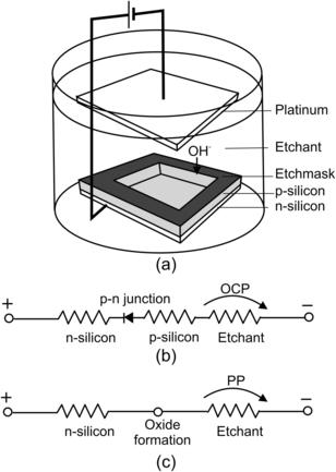 |
| FIGURE 4.3 |
The above-mentioned electrochemical characteristics can be used for controlling etch stop with a p–n junction as described in Fig. 4.3 (a). Because the p–n junction is reverse biased, most of the voltage drops at this junction. Thus, p-silicon is allowed to float at OCP and is etched away (Fig. 4.3 (b)). Etching away p-silicon destroys the p–n junction. The voltage across the two electrodes drops to a PP value. The subsequent formation of silicon oxide on the surface automatically stops the etching process as schematically depicted in Fig. 4.3 (c).
A further approach of generating holes in silicon is photon pumping. Holes are generated in positive bias n-silicon by illumination. This technique was utilized for fabricating high-aspect-ratio structures [18].
4.1.2.2. Dry etching
In dry etching, etchant gases or plasmas remove substrate materials. Generally, dry-etching techniques are categorized as physical dry etching, chemical dry etching, and physical–chemical etching.
Physical dry etching utilizes the kinetic energy of particle beams, such as ion beam, electron beam, or photon beam, to attack the substrate surface. The high-energy particles knock out substrate’s atoms from its surface. The knocked-out material immediately evaporates after leaving the substrate surface. Since no chemical reaction is involved in this process, almost all materials can be removed by this technique. The main drawbacks are slow etch rates, low selectivity, and trench effects caused by reflected ions.
Chemical dry etching uses a chemical reaction between etchant gases to attack the substrate material. Gaseous reaction products are conditions for this etching concept because deposition of solid products will protect the surface and stop the etching process. Chemical dry etching is isotropic and exhibits relatively high selectivity. Etchant gases either can be excited in an RF field to become plasma or react directly with the etched material. Chemical dry etching is often used for cleaning wafers. For instance, photoresist and other organic layers can be removed with oxygen plasma. Table 4.5 lists some typical recipes of dry etchant gases.
| Material | Etchant Gases | Selective To |
|---|---|---|
| Si | BCl3/Cl2, BCl3/CF4, BCl3/CHF3, Cl2/CF4, Cl2/He, Cl2/CHF3, HBr, HBr/Cl2/He/O2, HBr/NFl3/He/O2, HBr/SiF4/NF3, HCl, CF4 | SiO2 |
| SiO2 | CF4/H2, C2F6, C3F8, CHF3, CHF3/O2, CHF3/CF4, (CF4/O2) | Si (Al) |
| Si3N4 | CF4/H2, (CF4/CHF3/He, CHF3, C2F6) | Si (SiO2) |
| Al | BCl3, BCl3/Cl2, BCl3/Cl2/He, BCl3/Cl2/CHF3/O2, HBr, HBr/Cl2, HJ, SiCl4, SiCl/Cl2, Cl2/He | SiO2 |
| Organics | O2, O2/CF4, O2,/SF6 | — |
Physical–chemical etching is further categorized as reactive ion etching (RIE), anodic plasma etching (APE), magnetically enhanced reactive ion etching (MERIE), triode reactive ion etching (TRIE), and transmission-coupled plasma etching (TCPE) [3]. RIE is the most important technique for micromachining. Reactant gases are excited to ions. Under low pressures and a strong electrical field, ions are directed to the substrate surface almost perpendicularly. Therefore, this method can achieve relatively high aspect ratios. The etch rates lie between the ranges of physical etching and chemical etching.
Dry etching using plasma is a better process for achieving precisely defined features. However, most conventional plasma-assisted dry-etching processes are isotropic, which limits their applications to etching of thin films. The common problem of physical–chemical dry etching (or RIE) used in microelectronics is the trench effect where etch trenches are not vertical. The trench is wider on the top because the top section of a trench is exposed longer to etching plasma and ions. The wall should be protected during the dry-etching process to keep trench walls parallel and to achieve a high aspect ratio. For microchannels, a special technique called deep reactive ion etching (DRIE) is needed for the fabrication of high-aspect-ratio structure. The DRIE process does not depend on crystal orientation of the wafers. Two major approaches of DRIE are:
• Etching assisted by cryogenic cooling;
• Alternate etching and chemical vapor deposition.
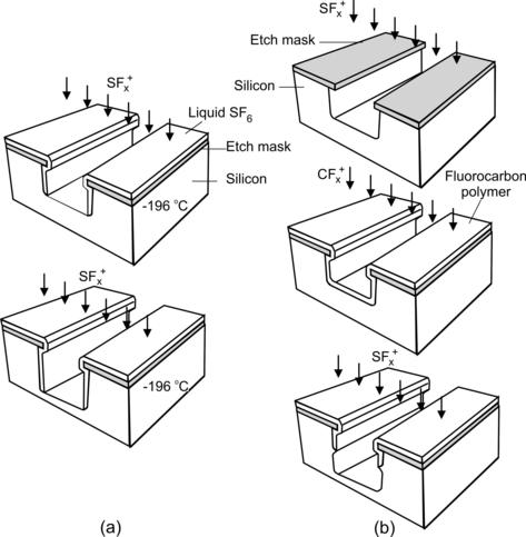
In the first approach, the substrate is cooled with liquid nitrogen. The cryogenic temperatures allow reactant gas, such as SF6 or O2, to condense on the trench surface. While the condensation film protects the sidewall from etching, it is removed at the bottom by ion bombardment. Because the trench bottom is not protected, it is etched further into the substrate (Fig. 4.4 (a)).
 |
| FIGURE 4.4 |
The second approach uses chemical vapor deposition to protect the sidewalls [19]. This technique was invented and patented by Robert Bosch GmbH in Reutlingen, Germany. Therefore, the technique is often called the Bosch process. The etch cycle consists of two steps: etching and deposition. In the etching step, silicon is removed by SF6. The etching step lasts from 5 to 15s, in which the etch front advances from 25 to 60nm in silicon. In the deposition step, supply gas is switched to C4F8. A film of fluorocarbon polymer of about 10nm is deposited on the trench wall. In the next cycle, the polymer film at the bottom surface is removed by ion bombardment, while the film at sidewalls is intact and protects the sidewalls from etching. In this way, the etch front advances into the substrate at rates ranging from 1.5 to 4μm/min (Fig. 4.4 (b)).
4.1.2.3. Bulk micromachined microchannels and nanochannels
Microchannels are the key components of a micromixer. This section illustrates the fabrication of microchannels in bulk silicon and glass using the techniques discussed in the previous sections. Both isotropic and anisotropic etching can be used to fabricate microchannels in bulk materials. A variety of cross-sectional channel shapes can be achieved by combining different micromachining techniques discussed previously.
Glass is a familiar material in chemistry and life sciences. Microchannels in glass have been used widely for applications in these fields [20] and [24]. Glass consists mainly of silicon dioxide and therefore can be etched with oxide etchants listed in Table 4.2. The microchannels in glass are sealed by thermal bonding to another glass plate. Most glass types can be etched in fluoride-based solutions [21] and [22]. Photolithography and subsequent etching can be used for photosensitive glasses, such as Foturan, to make microchannels [23].
Isotropic etching in silicon results in semicircular channel shapes similar to those of glass etching. Microchannels with trapezoidal cross-sections are formed by anisotropic etching of {100}-[23] or {110}-wafers [24]. Microchannels etched in silicon are sealed either by anodic bonding to a glass wafer or by thermal direct bonding to another silicon wafer. A glass cover is ideal for micromixers that need optical access to the flow in the microchannel.
Sealing microchannels with anodic bonding or direct bonding has a drawback of wafer-to-wafer misalignment. Misalignments and voids trapped during bonding processes can change the desired cross-sectional shapes and, consequently, the function of the intended micromixer. Fabrication of covered channels in a single wafer can overcome the problems associated with misalignment and wafer bonding. In general, these covered microchannels are fabricated and buried in a single substrate. Sealing is achieved by covering the etch access with a subsequent deposition process.
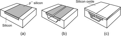
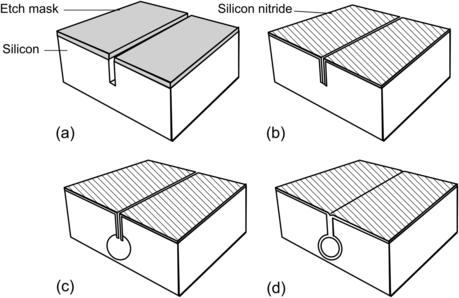
Figure 4.5 illustrates the main steps of making a buried channel in {100}-wafer. The process starts with a highly boron-doped silicon layer with a doping concentration higher than 7×1019cm–3 (Fig. 4.5 (a)). This layer works as etch stop and masking layer for the subsequent wet-etching process. Etch accesses are opened by RIE through the highly boron-doped layer. The buried channel is formed by anisotropic etching. The boron-doped layer remains intact during the etch process (Fig. 4.5 (b)). After anisotropic etching, the access gaps are sealed by thermal oxidation (Fig. 4.5 (c)). The final deposition of silicon nitride covers the entire structure [25]. The burying depth of the above-described channel depends on the thickness of the highly boron-doped layer, which is a maximum 5μm due to limits of diffusion processes [25] and [26]. The process shown in Fig. 3.6 overcomes this problem by using deep trenches etched by DRIE [27] and [28]. Figure 4.6 shows the basic steps of this technique. The process starts with DRIE of a narrow trench (Fig. 4.6 (a)). The depth of this trench defines the burying depth of the channel. In the next step, the trench wall is protected by deposition of silicon nitride or by thermal oxidation (Fig. 4.6 (b)). The layer at trench bottom is then removed by RIE to create the etch access. Anisotropic or isotropic etching can be used to form the channel (Fig. 4.6 (c)). After stripping the protecting layer, conformal LPCVD of silicon nitride seals the channel (Fig. 4.6 (d)). The advantage of this technique is that a network of channels can be fabricated at different depths in bulk silicon. Using this technique, complicated designs, such as a three-dimensional conduit of a micromixer based on chaotic advection, can be fabricated.
 |
| FIGURE 4.5 |
 |
| FIGURE 4.6 |
Because of the wavelengths on the order of few hundred nanometers, optical lithography cannot create nanochannels with widths on the order of several tens of nanometers. Interferometric lithography can be used for making structure size less than 100nm. Some other techniques with high-energy beams can also give a higher resolution. Direct writing with scanning electron beam lithography creates structures with 10-nm resolution. However, the throughput of this technique is extremely low due to its serial nature. X-ray lithography can deliver 50-nm resolution; however, such facility is expensive and impractical for mass production. Another technique for making nanostructures is called nanoimprint lithography or soft lithography. This technique uses a master, which is fabricated with the more expensive technologies such as electron beam writing. Resist patterns can be transferred by imprinting on a substrate surface. Open nanochannels can be fabricated by subsequent etching processes. The nanochannels are covered with a deposition process.
4.1.2.4. Epi-micromachining or near-surface micromachining
Epi-micromachining or near-surface micromachining is a technology that allows fabricating microstructures in a thin layer of 2–10 micrometers on top of a silicon wafer. The general concept of epi-micromachining is similar to that of polysilicon surface micromachining. Both need a sacrificial layer beneath the functional layer. After structuring the functional layer and etching away the sacrificial layer, a freestanding component can be released. Thus, having a sacrificial layer and ensuring the selectivity to the functional layer are important for epi-micromachining.
4.1.3. Polysilicon
4.1.3.1. Polysilicon surface micromachining
Polycrystalline silicon is referred to as polysilicon, which is deposited during an LPCVD process with silane. The deposition temperatures range from 575°C to 650°C. At temperatures below 575°C, the silicon layer is amorphous. Above 650°C, polycrystalline has a columnar structure. The grain size is typically between 0.03 and 0.3μm. After annealing at 900–1000°C for several minutes, crystallization and grain growth occur. The grain size is then on the order of 1μm. Polysilicon can be doped in situ with the same gases used for epitaxial silicon. The deposition rates range from 10 to 20nm/min [4].
Polysilicon layers are generally conformal. In surface micromachining, polysilicon is used directly as mechanical material. For fabrication of micromixers, polysilicon can be used for making channel walls and sealing etched channel structures. Devices made of polycrystalline silicon (or polysilicon) are mostly fabricated with the traditional surface micromachining. The term “traditional” is used here because the same fabrication concept with a sacrificial layer has also been used recently for polymer and metallic structures. A surface micromachining process starts with the deposition of a sacrificial layer (Fig. 4.7 (a)). The sacrificial layer can be structured to generate anchor points for the later functional structure. Subsequent deposition and patterning of the functional layer define the microstructures (Fig. 4.7 (b)). Removing the underlying sacrificial layer releases the freestanding microstructures (Fig. 4.7 (c)).
 |
| FIGURE 4.7 |
The main advantage of surface micromachining based on polysilicon is compatibility to CMOS processes. The well-established CMOS techniques, such as reactive ion etching (RIE), allow the fabrication of very small structures with sizes on the order of 1μm. There are a few challenges in polysilicon surface micromachining. First, very long etching time is required for a flat and large area. Thus, designing etch access into the MEMS structure is necessary for reducing the etching time. Since the sacrificial layer (commonly, silicon oxide or phosphorous-doped silicon oxide) and the polysilicon layers are deposited under different conditions, it is important to deposit a stress-free polysilicon layer. The stress after deposition can be removed by subsequent annealing up to a temperature where crystallization starts.
The last problem is in the release step. The sacrificial etching process and the subsequent rinsing process are both wet processes. While drying, the liquid bridge between the freestanding structure and the substrate causes it to collapse and stick to the surface. There are several solutions for this problem. Dry etchant, such as vapor phase HF, can be used to avoid the liquid phase. However, gaseous HF also attacks silicon nitride. Thus, silicon nitride should not be exposed to HF during the release process. Solvents with lower surface tension, such as methanol, can be used for the rinsing process. Dimples can be introduced in the design to avoid stiction. Alternative drying techniques, such as CO2 critical drying and freeze drying, can avoid the liquid phase. An organic film can work as sacrificial layer, which only requires dry oxygen plasma for removal. Finally, surface modification with a self-assembled monolayer (SAM) can minimize the surface energy and consequently stiction.
4.1.3.2. Fabrication of microchannels with silicon surface micromachining
A general surface micromachining process for microchannels starts with deposition of the sacrificial layer (Fig. 4.8 (a)). The channel material is then deposited over the structured sacrificial layer. After opening etch accesses through the channel wall, the sacrificial layer is etched to hollow out the channel. A subsequent deposition of channel material seals the etch access.
 |
| FIGURE 4.8 |
Lin et al. reported the fabrication of a microchannel in a microneedle using the above technique [29]. PSG is deposited as the sacrificial layer over a ground silicon nitride layer. The structured sacrificial layer is then encapsulated by LPCVD silicon nitride. Etch access is opened with RIE of the nitride wall. After removing the sacrificial PSG, a second LPCVD process seals the empty channel with silicon nitride. In a similar process, the channel is underetched, resulting in a suspended nitride channel [30].
The above approach can be further developed using silicon substrate directly as sacrificial material [28]. The mold is fabricated in a handle wafer with bulk micromachining. The channel wall is defined by deposition of nitride/oxide double layer (Fig. 4.8 (b)). With silicon dioxide on top, the silicon wafer is bonded anodically to a glass wafer. Etching away the silicon handle wafer releases the nitride/oxide channel on glass. If the channel wall is too thin for certain applications, the surface of the structure on glass can be coated with a thick polymer layer [31].
Besides the above techniques, microchannels with reasonable heights can be fabricated in metals with the process described in [32]. The process starts with deposition of a metal seed layer on the substrate (Fig. 4.8 (c)). A subsequent electroplating process defines the bottom wall of the channel. Next, a thick-film photoresist, such as AZ4620, is deposited and developed to form the sacrificial structure for the channel. Gold is then sputtered on the resist structure as the second seed layer. Electroplating on this seed layer forms the sidewall and top wall of the channel. Etching the gold layer exposes the sacrificial photoresist. Removing photoresist with acetone creates a hollow metal channel. A similar technique was used in [33] to fabricate more sophisticated microfluidic devices, such as microvalves.
4.1.4. Other materials
4.1.4.1. Diamond thin films
Silicon-based devices have poor mechanical and tribological properties. Due to the prominent surface effects, microdevices usually avoid large deflection and extensive sliding as well as rolling contacts. Compared to silicon, carbon has superior properties. For instance, the coefficient of friction of single-crystal diamond is on the order 0.01, which makes the wear life of a diamond-coated surface four orders of magnitude higher than silicon [34]. Diamond film may be a good candidate for making micromixers for extreme conditions. Diamond microstructures can be fabricated using thin film deposition. Diamond thin films made with chemical vapor deposition methods have polycrystalline characteristics and are categorized as microcrystalline diamond (MCD) and ultrananocrystalline diamond (UNCD). The grain sizes of MCD and UNCD are on the order of several micrometers and nanometers, respectively.
The easiest method is to coat a silicon-based component with a thin diamond film. This method utilizes the well-established silicon technology but provides components with superb surface properties. Microcomponents can be fabricated based on UNCD by selective deposition and lithographic patterning.
Selective deposition can be achieved by controlling the seeding layer before deposition. The growth of diamond films requires a seeding layer, which is formed by exposing the substrate to a suspension of fine diamond particles. The seeding layer can be patterned by:
• Selected seeding with a photoresist mask,
• Using diamond-loaded photoresist and subsequent photolithographic patterning, and
• Selective etching of the seeding layer.
Diamond film can be doped with nitrogen to become electrically conductive. Combining with a sacrificial layer, these technologies allow making diamond-based devices in the same way as polysilicon surface micromachining. Diamond-based technologies also allow the fabrication of basic electronic components, such as diodes and transistors. Electronic components make this technology suitable for more complex diamond-based devices. A recent review on diamond-based semiconductor technology was given by Gurbuz et al. [35].
4.1.4.2. Silicon carbide
Silicon carbide SiC poses excellent electrical, mechanical, and chemical properties. Thus, devices based on silicon carbide can be used in harsh environments at high temperature and pressure. Silicon carbide sublimes at around 2000°C, which is much higher than the melting temperature of silicon (1410°C). Silicon carbide is therefore suitable for making micromixers, which are used as microreactor with extremely high operation temperatures.
Silicon carbide wafers are commercially available in both single-crystalline and polycrystalline forms. However, similar to polysilicon-based and diamond-based MEMS, the growth of a thin silicon carbide film is important for making SiC devices. Epitaxial SiC can be deposited in a CVD process on a SiC wafer or on a silicon wafer with a SiC seeding layer. Micromixers may not need the high quality of epitaxial SiC, and amorphous and polycrystalline SiC film can be the economical choice for the fabrication. There are a wide range of deposition techniques for polycrystalline and amorphous SiC, such as sputtering, reactive sputtering, reactive evaporation, CVD, LPCVD, APCVD, and PECVD [36].
With the availability of SiC wafer and SiC film, both bulk micromachining and surface micromachining are possible. The extremely high temperature required for etching of SiC makes chemical etching impractical for bulk micromachining of SiC. The only etching method available for room temperature is photoelectrochemical etching (PEC) for n-type SiC and dark electrochemical etching for p-type SiC [37]. Combining the deposition of thick-film SiC and silicon micromachining, a bulk SiC microcomponent can be fabricated. First, a mold is etched in the silicon substrate using DRIE. Next, SiC is deposited to fill the mold. After polishing away excess SiC, the mold is dissolved in a silicon etchant such as KOH, releasing the SiC component [38].
Silicon carbide surface micromachining can be realized with polysilicon as sacrificial layer and RIE for etching the SiC functional layer. Plasma chemistries with fluorinated compounds, such as CHF3, SF6, CF4, CBrF3 and NF3, and oxygen, are often used. Due to the high oxygen content, conventional photoresist cannot be used for masking purpose. A hard mask made of a metal, such as Al or Ni, is needed to withstand the oxygen plasma.
For application in life sciences, biocompatibility is an issue for selecting the right material for a micromixer. The biocompatibility of the materials used in silicon-based devices, such as single-crystalline silicon, polysilicon, silicon dioxide, silicone nitride, and silicon carbide, was evaluated according to ISO 10993 standards by Kotzar et al. [39]. Using mouse fibroblasts in the tests, none of the materials were found to be cytotoxic. An in vivo test based on implantation in rabbit muscle showed no sign of irritation. Only silicone nitride and SU-8 showed detectable nonvolatile residues. Further in vivo studies using stainless-steel cages [40] and Teflon cages [41] reveal that silicon, silicon nitride, silicon dioxide, gold, and SU-8 are biocompatible. However, silicon and SU-8 have shown increased biofouling. For more details on technologies and biocompatibility issues, the reader is referred to a recent review by Grayson et al. [42]. The good biocompatibility of devices made with common micromachining technologies allows the exploration of these technologies [43].
4.2. Polymeric Microtechnologies
Micromixers based on silicon and other inorganic materials have the drawbacks of higher cost and biocompatibility. For mass production of the relatively large devices for applications in analytical chemistry and biomedical diagnostics, polymers offer a real alternative to silicon-based substrates. Polymers are macromolecular materials, which are formed through polymerization reactions. In a polymerization reaction, the monomer units connect each other either in linear chains or in three-dimensional network chains and form a macromolecule. For devices in biomedical applications, materials such as silicone rubber, polycarbonate, and polyimide are inexpensive and disposable [44]. According to the behaviors of interconnects between monomers and subsequently molding behaviors, polymers are categorized as thermoplastics, elastomers, and thermosets.
Polymers as functional materials fulfill a number of requirements of devices for chemical and biomedical applications:
• Polymers are suitable for bulk and surface micromachining.
• Many polymers are optically transparent.
• Most polymers are good electrical insulators. They can also be modified to be electrically conductive.
• The surface chemistry of polymers can be easily modified for a certain application.
Shape memory polymers (SMPs) are interesting materials with possible applications in active micromixers. Similar to shape memory alloys, SMPs are activated thermally. SMPs have a morphology consisting of a shape-fixing matrix phase and a shape-memorizing dispersed phase. The shape-memorizing phase consists of crosslinks that remember a primary shape of the SMP. The polymer can be brought from a primary shape into a secondary shape at a temperature above the transition. The secondary shape is locked by cooling the SMP under the transition temperature. Heating the SMP above the transition temperature again brings it back to the primary shape [45].
The advances in polymeric electronics allow the integration of electronic components into an all-polymeric system. For recent works on polymeric electronics, the reader is referred to the recent review by Facchetti et al. [46]. In the field of bioengineering, polymeric technologies can provide scaffold structures for growing and harvesting tissues.
4.2.1. Thick-film polymeric materials
4.2.1.1. Polymethylmethacrylate (PMMA) resist
Polymethylmethacrylate (PMMA) is well known by a variety of trade names such as Acrylic, Lucite, Oroglas, Perspex, and Plexiglas. PMMA can be used as a substrate material or as a thick-film resist for the LIGA technique [47].
A thick PMMA film can be deposited on a substrate by different methods: multiple spin coating, prefabricated sheets, casting, and plasma polymerization. Since multilayer spin coating is achieved with several coating steps, the multiple layers cause high interfacial stresses and lead to cracks. The problem with the cracks can be avoided by using a preformed PMMA sheet, which is bonded to the substrate [48]. Monomer MMA (methylmethacrylate) can be used as the adhesive material for the bonding process [49]. PMMA can also be polymerized in situ with casting resin [50] or with plasma [51].
Structuring PMMA requires collimated X-ray with wavelengths ranging from 0.2 to 2nm, which are only available in synchrotron facilities. X-ray also requires special mask substrates such as beryllium and titanium, which further increases the cost of this technique. The beryllium mask with its higher Young’s modulus and thickness is optimal for X-ray lithography. The absorbant material of an X-ray mask can be gold, tungsten, or tantalum. The thicker the absorber layer, the stronger the X-ray energy can be used, and, consequently, the higher is the aspect ratio of the structures in PMMA. The high-energy X-ray breaks down the polymer chains in the exposed area, which is chemically etched in the development process. The typical developer consists of a mixture of 20 vol% tetrahydro-1,4-oxazine, 5 vol% 2-aminoethanol-1, 60 vol% 2-(2-butoxy-ethoxy) ethanol, and 15 vol% water [52]. The limited access and costs of a synchrotron facility are the main drawbacks of the LIGA technique in general and PMMA as polymeric structural material in particular. A low-cost alternative to X-ray is direct ablation using laser. Laser micromachining of PMMA will be discussed later in this chapter. Thick-film resists, such as SU-8 and the AZ-4000 series, have the advantage of using low-cost UV exposure. However, structure heights and aspect ratios of UV exposure cannot meet those of PMMA with X-ray exposure.
4.2.1.2. SU-8 resist
In contrast to PMMA, a thick SU-8 layer can work with conventional UV light as the exposure source. SU-8 is a negative photoresist based on EPON SU-8 epoxy resin for the near-UV wavelengths from 365 to 436nm. At these wavelengths, the photoresist has very low optical absorption, which makes photolithography of thick films with high aspect ratios possible [53]. Structure heights up to 2mm with an aspect ratio better than 20 can be achieved with standard lithography equipment [54] and [55]. Photoresists, such as SU-8, are epoxy resins, which are molecules with one or more epoxy groups. During the curing process, epoxy resins are converted to a thermoset form. SU-8 photoresist consists of three basic components: an epoxy resin, such as EPON SU-8; a solvent, such as gamma-butyrolactone (GBL); and a photoinitiator, such as triarylium–sulfonium salt.
SU-8 photoresists are commercially available with different viscosities. A standard SU-8 process consists of the following steps: spin coating, soft bake, exposure, post-exposure bake, developing, and hard bake.
During the spin-coating process, the film thickness is determined by the viscosity of the photoresist and the spin speed. Higher viscosity or lower spin speed results in a thicker resist film. After spin coating, the film is soft-baked to evaporate the solvent. Soft bake can be carried out on a level hot plate or in a convection oven. Two-step temperature ramping between 65°C and 95°C is recommended [56] and [57]. SU-8 can be exposed with I-line equipment, which uses a mercury lamp with near-UV wavelengths. Optical absorption of SU-8 increases sharply below 350nm. Therefore, wavelengths higher than 350nm should be used for the exposure. The thicker the film, the higher the exposure dose required. The exposed area of SU-8 film is selectively crosslinked by a post-exposure bake. The crosslink process can cause high film stress, which damages the film with cracks. To avoid this problem, a two-step ramp between 65°C and 95°C [56] and [57] or between 50°C and 100°C is recommended. Furthermore, rapid cooling after PEB should be avoided. Immersion processes or spray processes can be used to develop the resist. Solvent-based developers, such as ethyl lactate and diacetone alcohol, dissolve areas that are not polymerized during exposure and PEB. If necessary, the developed structure can be hard-baked at elevated temperatures from 150°C to 200°C. However, hard baking can increase stress and cause cracks in structures [58]. Removing a polymerized SU-8 film is the most difficult process, because SU-8 film becomes highly crosslinked after exposure and PEB. Etching with acid solutions, RIE, and laser ablation [59] are some of the methods for removing SU-8.
Because of its simple processes and the relatively good mechanical properties, SU-8 is used as the structural material for many microfluidic applications. There are many fabrication examples where SU-8 was used as spacer or directly as channel material.
The simplest technique to form a microchannel with SU-8 is using the crosslinked SU-8 structure to define the channel’s sidewall. While the bottom wall is the glass or silicon substrate, the channel can be covered and sealed by another silicon and glass plate. Ayliffe et al. reported an LIGA-like [60] (Fig. 4.9 (a)). Starting with a glass wafer as substrate material, a metal seed layer was deposited (Fig. 4.9 (a,1)). Subsequently, SU-8 is spin-coated and structured (Fig. 4.9 (a,2)). This high-aspect-ratio SU-8 structure is used as a mold for electroplating of gold or other metals (Fig. 4.9 (a,3)). In the next step, SU-8 is etched in oxygen plasma using an aluminum mask to form the actual microchannel (Fig. 4.9 (a,4) and (a,5)). Finally, a glass plate covers the structure using adhesive bonding.
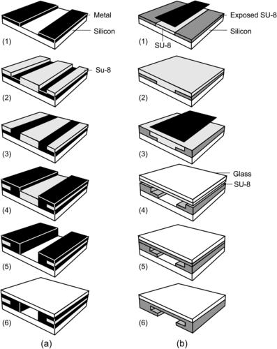 |
| FIGURE 4.9 Fabrication of microchannel with SU-8: (a) single layer combined with electroplating (after [59]) and (b) multiple layer. (after [60]) |
In the above example, microchannels are etched by oxygen plasma. An alternative is patterning by photolithography and development. Figure 4.9 (b) shows a fabrication process that uses two SU-8 layers to form a microchannel with a complex cross-section [61]. To start with, the first SU-8 layer is coated and exposed with the first mask (Fig. 4.9 (b1)). The next layer is spin-coated on top of the first layer (Fig. 4.9 (b2)). Since the second exposure may affect the structure defined by the first mask, the mask for the second layer should cover completely the unexposed areas of the first layer to avoid double exposure (Fig. 4.9 (b3)). After exposure of the second layer, the two layers are developed together to form the T-shape microchannel. The channel is then covered by a glass plate, which has a thin unexposed SU-8 layer as the adhesive layer (Fig. 4.9 (b4)). This thin adhesive layer is crosslinked by a blanket exposure through the glass plate. To form an optically transparent device, the silicon substrate can be etched away to yield an optically transparent device.
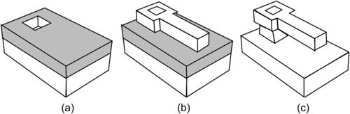
Three-dimensional structures can be constructed by multilayer exposure and embedded mask, as shown in Fig. 4.9 (a). As mentioned above, the problem of multilayer exposure is that the mask of the later layer should cover completely the previous layers to protect their unexposed areas. This means that direct fabrication of a closed structure, such as a covered channel, is not possible with conventional glass masks. One solution for the double-exposure problem is the use of an embedded mask [62] and [63]. The process starts with the exposure of the first SU-8 layer to form the bottom of the channel (Fig. 4.10 (a,1)).
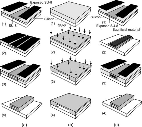 |
| FIGURE 4.10 Fabrication of covered channels with SU-8: (a) with embedded mask (after [62]); (b) selective proton writing (after [65]); and (c) with sacrificial layer. (after [63]) |
After the second layer is coated, the embedded mask is deposited and structured. A thin metal layer, such as gold [62], can be sputtered on the second SU-8 layer. This metal layer is patterned by common photolithography and etching. The patterned metal layer is used as an embedded mask for the subsequent exposure of the second SU-8 layer (Fig. 4.10 (a,2)). A third SU-8 layer is spin-coated and exposed to fabricate the top wall of the channel (Fig. 4.10 (a,3)). In the final step, all three layers are developed in a single process, resulting in a covered microchannel. The embedded mask is washed away after the developing process (Fig. 4.10 (a,4)). Instead of the embedded metal mask, an antireflection film, such as CK-6020L resist (FujiFilm Olin Inc., Japan), can be used for making covered SU-8 microchannel [64]. The use of antireflection coating ensures that this coating and the structural SU-8 can be developed at the same time.
The penetration depth of an energy beam depends on its intensity and determines the thickness of the crosslinked layer. A covered channel can be fabricated with selective proton writing or proton beam micromachining [65]. Similar to near-UV exposure, a proton beam also causes polymerization in SU-8. The depth of the polymerized area depends on the proton beam energy. This feature is used to form a three-dimensional structure in SU-8. Figure 4.10 (b) illustrates the relatively simple steps of this technique. To start with, the SU-8 layer is spin-coated on the substrate (Fig. 4.10 (b,1)). Writing with low energy forms the top of the channel. With low energy, a proton beam can only penetrate shallowly into the SU-8 layer and forms a thin polymerized layer (Fig. 4.10 (b,2)). Next, the proton beam with higher energy polymerizes the sidewalls of the channel. The high energy allows the beam to penetrate through the SU-8 layer down to the substrate surface (Fig. 4.10 (b,3)). In the final step, the exposed SU-8 is developed, resulting in a covered microchannel (Fig. 4.10 (b,4)).
Another method uses a sacrificial layer [63] and [64] to fabricate a closed SU-8 channel. The first SU-8 layer is coated, exposed, and developed to form the bottom of the channel (Fig. 4.10 (c1)). Subsequently, a sacrificial structure is deposited and patterned (Fig. 4.10 (c2)). The sacrificial material can be thermoplastics, waxes, epoxies [63], or positive photoresist [65]. Because of the self-planarizing nature of an unexposed SU-8 film, the sidewalls and the channel ceiling are formed with a single coating of a second SU-8 layer (Fig. 4.10 (c3)). After developing the second layer, the sacrificial material inside the channel is removed, leaving a closed SU-8 microchannel (Fig. 4.10 (c4)).
4.2.1.3. Other thick-film resists
Another commercially available thick-film resist is AZ4562 (Clariant, Charlotte, North Carolina), which is a positive photoresist. This resist belongs to the Novolak resist system, which is in common with most commercially available positive resists. Using multilayer spin coating, thick resist layers up to 100μm can be achieved. This photoresist has no oxygen sensitivity, but a high resistance to plasma etching, good adhesion properties, and high-resolution capability [66]. AZ4562 is typically used either as a mold for subsequent metal electroplating [67] and [68] or as master templates for micromolding. Table 4.6 gives a summary of the parameters of PMMA, SU-8, and AZ4562.
AZ9260 is the other Novolak photoresist from Clariant, which exhibits a better transparency than AZ4562, and, therefore, promises a better aspect ratio. Aspect ratios up to 15 are achieved with a film thickness of 100μm [68]. A theoretical thickness of 150μm is expected from this photoresist.
Ma-P100 (Microresist Technology, Berlin, Germany) is the other photoresist that can give structure heights up to 100μm. This photoresist has aspect ratios on the order of 5, poorer than that of the AZ family [69].
4.2.2. Polymeric bulk micromachining
In contrast to many other microdevices, micromixers are large, due to their usually long microchannels. The sample volume required for detectability needs relatively large reservoirs. Therefore, the cost of the substrate material plays an important role for large-scale production. For the same surface area and optical transparency, a glass substrate may cost 10–100 times more than a polymer substrate. Besides the cost advantage, polymers are available with a wide range of properties. Surface properties of polymers can be tailored for specific applications. As low-cost materials, polymers can be used directly as mechanical materials. Their electrical and chemical properties are interesting for physical, chemical, and biochemical sensing [5]. Polymer membranes and matrices are widely used in macroscale for the separation of DNA and proteins [6].
Polymers are organic materials consisting of macromolecules, which may have more than 1000 monomeric units. The crosslinking process of the monomers is triggered chemically by an initiator substance, or physically by photons, pressure, or temperature. In a polymerization reaction, monomer units react to form linear chains or three-dimensional networks of polymer chains. If only one type of polymer is used, the material is called homopolymer. Polymerization of two or more monomer units results in a copolymer. Polymers containing specific additives are called plastics. Polymers exist in two basic forms: amorphous and microcrystalline. The macromolecules in a polymeric material have different lengths. Thus, there is no fixed melting temperature for polymers. Several temperatures exist in the melting process of a polymeric material. The characteristic lower and upper temperatures of a polymeric material are the glass transition temperature and the decomposition temperature. At the glass transition temperature, the material still keeps its solid shape but loses its crosslinking strength. A further increase in temperature damages the bondage between the monomers, and the plastic will lose its solid shape. Above the glass transition temperature, a polymeric material becomes soft and can be machined by molding or hot embossing. The glass transition temperature can be adjusted by mixing a softener with the original polymeric material. Above the decomposition temperature, the polymeric material starts to degrade and ceases to function.
Based on their molding behavior, polymers can be categorized into three groups: elastomeric materials, duroplastic materials, and thermoplastic materials. Elastomeric materials or elastomers have weakly crosslinked polymer chains. These polymer chains can be stretched under external stress, but regain their original state if the stress is removed. Elastomeric polymer does not melt before reaching decomposition temperature. Elastomeric materials are suitable for prototyping of microfluidic devices. The elastic property is ideal for sealing of the fluidic interfaces. In contrast to elastomeric materials, duroplastic materials or duroplastics have strong crosslinked polymer chains. Duroplastics do not soften much before decomposition temperature. They are strong and brittle. The properties of thermoplastic materials are ranked between the above two extremes. The material consists of weakly linked polymer chains. Thus, thermoplastics can be softened and structured at temperatures between the glass transition point and decomposition point. Due to this characteristic, thermoplastic polymers are commonly used for micromolding.
Most micromixers used for chemical analysis and life sciences require an optically transparent material. Many polymers are self-fluorescent at low excitation wavelengths. Self-fluorescence may affect the sensitivity of microfluidic applications with fluorescent detection. The next drawback of polymers is their poor chemical resistance to solvents. With applications in the chemical industry and drug discovery, micromixers may need to handle a variety of solvents. In this case, glass and silicon are the materials of choice. Polymers are usually not a material of great endurance. For long-term applications, aging, low chemical resistance, and low UV resistance will be the main problems of using polymers as substrate material.
Surface properties play an important role for devices utilizing electroosmotic pumping. A high charge density on the surface assures a stable and controllable electroosmotic flow. Furthermore, a surface with patterned zeta potential is vital for designing electrokinetic micromixer based on chaotic advection. Due to the lack of ionizable groups, most polymers have a lower surface charge density compared to glass. Thus, for applications with electroosmotic flows, such as CE separation, the surface of the polymeric substrate should be treated accordingly.
The major advantage of polymeric micromixers compared to silicon-based or glass-based counterparts is their superior biocompatibility. Polymeric devices are best for DNA analysis, polymerase chain reactions, cell handling, and clinical diagnostics. Many polymers are compatible to blood and tissue. Micromachining of these materials may make implantable microfluidic devices for applications such as drug delivery possible. Table 4.7 lists the properties of some typical polymers.
There are two key approaches in polymeric bulk micromachining: dry etching with oxygen plasma and replication. Similar to silicon-based bulk micromachining, polymeric bulk micromachining uses photolithography and etching to transfer a pattern into the bulk substrate. Oxygen plasma can be used for etching polymers and other organic materials. Because photoresists are organic, a hard mask made of metals such as aluminum, nickel, or titanium should be used here. Figure 4.11 shows an example of the fabrication of a microchannel with two access holes in a bulk polymeric material. To start with, a metal layer is deposited on the polymer surface. Sputtering is preferred because a low temperature is required for processing polymers. The metal layer is patterned and structured using conventional lithography and etching techniques (Fig. 4.11 (a)). The two access holes are first etched with oxygen plasma (Fig. 4.11 (b)). The metal layers are then etched to form the mask for the microchannel. Access holes and microchannel etched until the areas of the access holes are opened on the backside of the substrate (Fig. 4.11 (c)). Finally, the mask is etched away and the microchannel can be sealed by thermal bonding to another polymer sheet (Fig. 4.11 (d)).
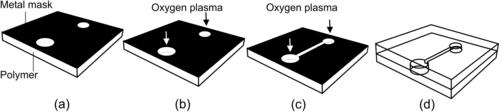 |
| FIGURE 4.11 |
The basic idea behind replication technologies is the combination between the more expensive silicon-based technology and the low-cost replication in polymers. The few drawbacks of replication technologies are:
• Since the master is to be removed from the molded structures, freestanding structures with undercuts cannot be fabricated. A combination with polymeric surface micromachining could be a solution for this problem.
• Only few micromachining technologies can meet the required smoothness of the master mold.
• Due to contamination and fast diffusion in microscale, release agents used in macroscale cannot be used for the release process in microscale.
The mold can be fabricated in silicon with the established micromachining techniques. Conventional machining techniques such as drilling, cutting, milling, and turning can be used for structures down to several tens of microns. Bulk silicon micromachining can be used for structures with high aspect ratios. Metal mold can be electroplated with the help of a structured thick resists such as SU-8 and PMMA. For instance, the fabrication of nickel mold from structured PMMA was established and called LIGA (Lithographie-Galvanoformung-Abformung, German acronym for lithography, electroplating, and molding). In the following, three replication techniques are discussed in detail: injection molding, hot embossing, and soft lithography.
4.2.2.1. Injection molding
Injection molding is carried out at temperatures above the glass transition temperatures of amorphous thermoplastics such as polymethylmethacrylate (PMMA), polycarbonate (PC), and polysulfone (PSU). For semicrystalline thermoplastics, such as polyoxymethylene (POM) and polyamide (PA), the molding temperature should be higher than the crystallite melting point [79]. Table 4.8 compares the characteristics of different polymers commonly used for micromolding.
| Polymers | PMMA | PC | PS | COC | PP |
|---|---|---|---|---|---|
| Heat resistance (°C) | 105 | 140 | 100 | 130 | 110 |
| Density (kg/m3) | 1,190 | 1,200 | 1,050 | 1,020 | 900 |
| Refractive index | 1.42 | 1.58 | 1.59 | 1.53 | opaque |
| Resistant to: | |||||
| Aqueous solutions | yes | limited | yes | yes | yes |
| Concentrated acids | no | no | yes | yes | yes |
| Polar hydrocarbons | no | limited | limited | yes | yes |
| Hydrocarbons | yes | yes | no | no | no |
| Suitable for micromolding | moderate | good | good | good | moderate |
| Permeability coefficients (×10–17m2/s – Pa): | |||||
| He | 5.2 | 7.5 | — | — | — |
| O2 | 0.12 | 1.1 | — | — | — |
| H2O | 480–1,900 | 720–1,050 | — | — | — |
| Hot-embossing parameters: | |||||
| Embossing temperature (°C) | 120–130 | 160–175 | — | — | — |
| Deembossing temperature (°C) | 95 | 135 | — | — | — |
| Embossing pressure (bars) | 25–37 | 25–37 | — | — | — |
| Hold time (s) | 30–60 | 30–60 | — | — | — |
Mold inserts for injection molding can be fabricated with common microtechnologies such as bulk micromachining and LIGA. Alternatively, bulk-micromachined parts can be used as masters for electroplating [80]. After separation from the silicon part, the metal parts can be used as negative mold inserts to fabricate replicas of the silicon parts [80]. Structures in micromixers may have high aspect ratios and very small filling channels. Together with the high viscosity of melted plastics, high pressures are required for the injection. To avoid the high pressure associated with the high viscosity, reaction injection molding (RIM) can be used. This technique involves mixing of two or more reactive chemicals. The mixture flows into the mold at relatively low temperature, pressure, and viscosity. Curing occurs in the mold at relatively low temperatures and pressures. The excess prepolymers are fed back in a recirculation loop by pumps. The entire process, from mixing to demolding, typically takes less than one minute. The low processing viscosity allows good filling and high molding accuracy.
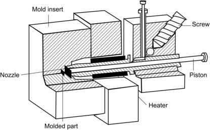
Figure 4.12 shows the schematics of a typical injection molding system. The machine consists of a screw, an injection nozzle, a heater, and a mold insert. To start with, polymer pellets are loaded into the screw. The piston pumps the polymer into the accumulation zone, where it is melted by a heater. If the desired polymer amount is reached, the piston moves forward and pushes the polymeric melt into the mold cavity through the nozzle. The required pressure is typically on the order of 500–2,000 bars [81] and [82]. After cooling, the melt solidifies, and can be taken out from the mold.
4.2.2.2. Hot embossing
Hot embossing was widely used for the fabrication of simple microchannels. The technique uses a master mold and a flat polymer substrate. The polymer substrate is heated above the glass transition temperatures of the substrate material. The glass temperature is typically in the range from 50°C to 150°C. Embossing force (0.5 to 2 kN/cm2) is then applied on the substrate under vacuum conditions. Before release, the master and the substrate are cooled under the applied embossing force. The entire hot-embossing process takes about few minutes [83], [84] and [85]. The vacuum is needed due to the formation of gas bubbles in the small structures. The vacuum also prevents corrosion of the master. The drawback of this technique compared to injection molding is the relatively long cycle time on the order of several minutes.
The most important parameters of hot embossing are embossing temperature, deembossing temperature, embossing pressures, and hold time. Table 4.8 lists the typical values of these parameters for hot embossing of PMMA and PC. Hot embossing can only make open channel structures. Fabricating covered channels and fluidic interconnects needs additional packaging techniques, such as thermal bonding to a sheet of the same material at temperatures above the glass temperature.
Injection compression molding combines the advantages of both injection and hot embossing. The polymer melt is first injected into the mold. The mold melt is then compressed to shape the final part. The low viscosity of the melt results in good filling in the molded part.
4.2.2.3. Soft lithography
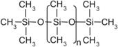
Soft lithography is a direct pattern transfer technique. The term “soft” refers to an elastomeric stamp with patterned relief structures on its surface. Polydimethylsiloxane (PDMS) has been used successfully as the elastomeric material. PDMS exhibits unique properties suitable for this purpose. PDMS has an inorganic siloxane backbone with organic methyl groups attached to silicon (see Fig. 4.13). Both prepolymers and curing agents are commercially available. PDMS has high optical transparency above a wavelength of 230nm and low self-fluorescence. PDMS has a low interfacial free energy, which avoids molecules of most polymers sticking on or reacting with its surface. The interfacial free energy of PDMS can be manipulated with plasma treatment. The modified surface properties of PDMS are needed for certain applications. PDMS is stable against humidity and temperature. This material is optically transparent and can be cured by UV light. PDMS is an elastomer and can therefore attach on nonplanar surfaces. PDMS is mechanically durable. These characteristics make PDMS an ideal material for soft lithography [86].
PDMS also has a number of drawbacks, such as swelling, shrinking, and elastic deformation. The design of a PDMS part should consider the shrinking effect upon curing. A number of organic solvents can swell PDMS as well. Furthermore, elastic deformation can limit the aspect ratio of the designed structure. A very high aspect ratio leads to the pairing effect, in which two parallel structures attach to each other, while a very low aspect ratio leads to sagging of noncontact regions, which makes further steps of soft lithography impossible. The recommended aspect ratios for PDMS structures are between 0.2 and 2 [86].
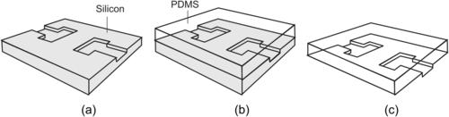
There are different techniques to transfer the pattern on this elastomeric stamp: microcontact printing and replica micromolding [86]. In many applications, the elastomeric PDMS part can be used directly as a microfluidic device with microchannels on it. Soft lithography is based on an elastomeric stamp with patterned relief structures on its surface. There are two basic techniques for transferring the micropatterns: microcontact printing and replica molding. In many polymeric devices, the elastomeric part can be used directly as the functional material. The fabrication process starts with the fabrication of a master using established technologies such as DRIE in silicon or photolithography of a thick-resist film such as SU-8. Polydimethylsiloxane (PDMS) is mixed from two prepolymers. The weight ratio of the base and the curing agent could be 10:1 or 5:1. Next, the PDMS mixture is poured into the master. PDMS is then cured at relatively low temperature from 60°C to 80°C for several hours. After peeling off and having surface treatment with low-temperature oxygen plasma, the structured PDMS membrane can be brought into contact with clean glass, silica, or another piece of surface-activated PDMS. The bond can withstand pressures up to five bars. Three-dimensional structures can be formed by lamination of many PDMS sheets. In this case, methanol helps to promote both bonding and self-alignment. The surface tension at superimposed holes in the PDMS sheets self-aligns them. Methanol prevents instant bonding between two PDMS sheets after plasma treatment. After evaporating methanol on a hot plate, the laminated stack is bonded.
The master for a PDMS device can be fabricated with conventional silicon-based micromachining technologies. Figure 4.14 depicts the basic steps of the fabrication of a PDMS part. The silicon master is silanized by exposure to the vapor of CF3(CF2)6(CH2)2SiCl3 for about 30minutes [85]. The prepolymer is coated on the silicon or glass master. After curing in an elevated temperature, the cured PDMS layer can be peeled off and is ready for the use in the subsequent steps.
The master can also be fabricated with SU-8 [87]. The PDMS part is used directly as structural material. The PDMS device is bonded to a glass plate after oxidizing their surfaces with oxygen plasma. In a similar approach, three-dimensional structures are fabricated by the lamination of different structured PDMS layers. Fluidic interconnects are embedded directly in the PDMS device.
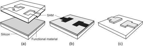
Microcontact printing utilizes the relief structures on the surface of the PDMS stamp to transfer a pattern of SAMs to the substrate surface by contact (Fig. 4.15 (a)). SAMs can be created by immersion of the substrate in a solution containing a ligand Y(CH2)nX, where X is the head group and Y is the anchoring group. The head group determines the surface property of the monolayer. The stamp is wetted with the above solution and pressed on the substrate surface (Fig. 4.15 (b)). Usually, the SAM layer is too thin for some applications. Thus, SAM can be used as a mask to transfer the pattern to an underlying functional layer. Because of its small thickness, SAM can be quickly destroyed by ion bombardment. Therefore, a SAM mask is not suitable for reactive ion etching but for wet chemical etching (Fig. 4.15 (c)). The thicker functional layer, in turn, can be used as a mask for the more aggressive RIE. The resolution of microcontact printing depends on the properties of the stamp material, and can reach several tens of nanometers.
Surface properties of patterned SAM can be used as templates for selective deposition of other materials. For example, a patterned hydrophilic SAM traps liquid prepolymer on its surface. After curing, a polymer structure is formed on top of the patterned SAM. Furthermore, patterned SAM can be used for controlled deposition of metals and ceramics by selective CVD.
Micromolding with a PDMS master can be categorized as replica molding, microtransfer molding, micromolding in capillaries, and solvent-assisted micromolding [86]. Replica molding uses the PDMS stamp as a replica master for a prepolymer, which is cured by UV exposure or by elevated temperature. This technique can achieve resolutions of less than 10nm. In microtransfer molding, liquid prepolymer is applied on the PDMS master. The prepolymer layer is planarized by removing the excess prepolymer. Only prepolymer trapped between the relief structures remains on the surface of the PDMS master. The master is then placed on a planar substrate. UV exposure or heating solidifies the prepolymer. Peeling off the elastic PDMS master results in polymer structures on the substrate surface. This method does not completely remove the excess prepolymer on top of the PDMS stamp. A thin polymer layer on the order of 100nm remains on the substrate surface. If the patterned polymer is to be used as a mask for subsequent etching, this thin polymer layer should be removed by oxygen plasma [86]. Micromolding in capillaries uses capillary forces to fill the gaps between the substrate and the PDMS master. First, the PDMS master is pressed tightly on a planar substrate. Elastic PDMS seals off walls and creates capillary channels. A drop of liquid prepolymer is placed at the ends of these channels and fills them automatically due to capillary forces. After curing and peeling off the PDMS master, polymer structures remain on the substrate surface. This technique can be used to pattern silicon and glass with different materials [86]. Solvent-assisted micromolding uses a solvent to wet the PDMS stamp and soften the structural polymer. The solvent only dissolves the structural polymer and not PDMS. The stamp is pressed on a polymer film, which dissolves in the solvent and fills the gaps between relief structures of the stamp. After dissipation and evaporation of the solvent, solid polymer remains on the substrate [86].
4.2.2.4. Fast prototyping of micromixers with soft lithography
Soft lithography is a popular method for rapid prototyping of microfluidic devices. The majority of reported lab-scale prototypes were fabricated with this method. PDMS is a good device material because it has a number of useful properties: low cost, low toxicity, transparency from the visible wavelengths into the near ultraviolet wavelengths, and chemical inertness. The fabrication cost is further reduced by using high-resolution laser-printed transparency mask. This type of low cost allows feature size on the order of 20μm.
First, PDMS is mixed from the two commercially available prepolymers. The weight ratio of the base and the curing agent is usually 10:1. A low-cost simple way is to fabricate the solid master structuring an SU-8 layer using lithography (Fig. 4.16 (a)). Glass posts are placed on the SU-8 master to define the access holes and the reservoirs. These reservoirs and access holes can also be punched later in the PDMS layer. The PDMS mixture is poured into the master and stands for a few minutes to self-level. The whole set is then cured at relatively low temperature (from 60°C to 80°C) for several hours. After peeling off and having surface treatment with low-temperature oxygen plasma (Fig. 4.16 (b)), the structured PDMS membrane is brought into contact with clean glass, silica, or another piece of surface-activated PDMS (Fig. 4.16 (c)). The sealed channel can withstand pressures up to five bars. Without surface treatment, PDMS also forms a watertight seal when pressed against itself, glass, or most other smooth surfaces. These reversible seals are useful for detachable fluidic devices, which are often required in research and prototyping.
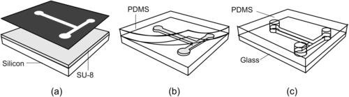
4.2.2.5. Laser machining
Laser machining is a localized, noncontact machining technique. Machining applications of laser include drilling, cutting, engraving, marking, and texturing. Almost all types of materials, such as metals, ceramics, plastics, and wood, can be used with laser machining. Most significantly, laser machining can remove materials in small amounts with a small heat-affected zone. Micromachining with controlled accuracy can be achieved. A further attractive advantage of laser machining compared to other micromachining techniques is the possibility of low-cost rapid prototyping. The disadvantage of laser machining is the re-deposition of substrate material, which makes the quality control of the machined surfaces difficult.
UV lasers were used to realize microstructures in polymers. Although UV laser is a good choice for laser ablation, its cost is much higher than that of CO2 laser. CO2 laser has a relatively long characteristic wavelength of 10.6μm. Thus, the ablation process is determined by the thermal energy of the laser beam. Therefore, the cross-section of the microchannel depends on the energy distribution of the laser beam, its moving speed, the laser power, and the thermal diffusivity of substrate material. The energy of the laser beam has a Gaussian distribution; thus, the cross-section of the channel also has a Gaussian shape (Fig. 4.17). Three types of lasers are commonly used for laser micromachining:
• Excimer lasers with ultraviolet wavelengths (351, 308, 248, 193nm);
• Nd:YAG lasers with near-infrared (1,067nm), visible (533nm), and UV wavelengths (355nm, 266nm); and
• CO2 lasers with deep-infrared wavelength (10.6μm).
The two major parameters of laser micromachining are wavelength and laser power. The choice of wavelength depends on the minimum structure size and the optical properties of the substrate material, such as absorption and reflection characteristics. Theoretically, the minimum achievable focal spot diameter and, consequently, the smallest size are about twice that of the laser wavelength.
The choice of power depends on the desired structure size and the ablation rate. When excimer or Nd:YAG lasers with a pulse duration of a few tens of nanoseconds are utilized, a single laser pulse will typically vaporize the surface material to a depth of 0.1–1μm (see Table 4.9). Since each pulse removes such a thin layer of material, the depth of the machined trench can be controlled accurately by the number of laser pulses. Furthermore, laser pulses of very short duration eliminate heat flow to surrounding materials. Consequently, clean and accurate structures can be achieved with shortly pulsed lasers. There are two modes of laser micromachining: direct writing and using a mask [99]. In the direct writing mode, the laser beam is focused on the substrate surface. The pattern is scanned using a precision x–y stage or galvano scanning mirrors. In this mode, the smallest structure depends on the accuracy of the scanning system, and is on the order of 25–50μm. In the masking mode, the mask determines the detailed shape of the structure. Therefore, the minimum structure size can be brought down to twice that of the laser wavelength.
| Material | Depth Per Pulse (μm) |
|---|---|
| Polymers | 0.3–0.7 |
| Ceramics and glass | 0.1–0.2 |
| Diamond | 0.05–0.1 |
| Metals | 0.1–1.0 |
Laser micromachining is suitable for fabrication of microchannels and fluidic access holes. An LIGA-like technique uses laser machining instead of X-ray lithography to machine PMMA [100]. Furthermore, the laser beam can be used for sealing polymeric devices fabricated with other techniques or making shadow masks.
4.2.3. Polymeric surface micromachining
Polymeric surface micromachining technique is similar to its silicon-based counterpart. A functional layer is structured on top of a sacrificial layer. Removing the sacrificial layer results in a freely movable structure. Polymers can work as both sacrificial and functional layers. With SU-8 as the functional layer, polymers, such as polystyrene, or metals, such as chromium, were used as sacrificial layers. Silicon was used directly as sacrificial material as well as the handling substrate for the fabrication of polymeric valves, polymeric micropumps, and polymeric microgrippers.
4.2.3.1. SU-8
SU-8 is a thick-film resist, which can be structured using UV lithography. With a Young’s modulus of 4–5 GPa and a Poisson’s ratio of 0.22, hardbacked SU-8 poses excellent mechanical properties and can be used for movable parts. The sacrificial material for the release of the SU-8 part can be the silicon substrate, a metal layer, or a polymer layer. Figure 4.18 (a) shows a micro-check valve made with this technology [71]. The valve was first structured on silicon substrate with a two-layer process. Developing both layers results in a three-dimensional valve structure with spring beams, a valve disk, and a sealing ring. Underetching silicon with KOH releases the valve. Circular access holes were placed on the structure for faster release. The smooth contours of the design help to arrest surface stress and avoid cracks in the structure.
 |
| FIGURE 4.18 |
For many applications, a metal layer on the structural polymeric material is needed. The metal layer can be structured to form electrodes and heaters. Figure 4.18 (b) shows an SU-8 microgripper, which has a thin metal layer on top acting as a heater [72]. Instead of silicon, a thin layer of polystyrene can be used as sacrificial layer. The polymeric sacrificial material can be dissolved by organic solvents such as toluene. In contrast to KOH for sacrificial silicon etching, solvent does not attack the thin metal layer.
4.2.3.2. Polyimide
Polyimide is available as photoresists such as Proimide 348 or 349 (Ciba Geigy) or PI-2732 (DuPont). Coating a single polyimide layer can result in a film thickness up to 40μm. This relatively thick film allows the use of photosensitive polyimide for the same purpose as other thick resists, such as SU-8 [73].
Fluorinated polyimide is optically transparent. This material can be machined by RIE. During an RIE process, fluorine radicals are released from the fluorinated polyimide and act as etchants [74].
Polyimide can work as a substrate material. Metals such as aluminum, titanium, and platinum can be sputtered on it [75]. Similar to other polymers, polyimide can be etched with RIE in oxygen plasma. Combining photolithography, RIE, and lamination, complex channel structures with metal electrodes can be fabricated in polyimide [76].
4.2.3.3. Parylene
Parylene is a polymer that can be deposited with CVD at room temperature. The CVD process allows coating a conformal film with a thickness ranging from several microns to several millimeters. Parylene is available as Parylene N, Parylene C, and Parylene D.
Parylene N is poly-paraxylylene, which is a good dielectric. Parylene N has a very low dissipation factor, high dielectric strength, and a frequency-independent dielectric constant. Parylene C is produced from the same monomer, modified only by the substitution of a chlorine atom for one of the aromatic hydrogens. Parylene C has a useful combination of electrical and physical properties, as well as a very low permeability to moisture and other corrosive gases. Parylene C is also able to provide a conformal insulation. Parylene D is modified from the same monomer by the substitution of the chlorine atom for two of the aromatic hydrogens. Parylene D is similar in properties to parylene C with the added ability to withstand higher temperatures. Deposition rates are fast, especially for parylene C, which is normally deposited at a rate of about 10μm/min. The deposition rates of both parylene N and parylene D are slower. Parylene can be used in microfluidic devices as a structural material, which offers low Young’s modulus. Such a soft material is needed in microvalves and micropumps. Furthermore, parylene coating can improve the biocompatibility of a microfluidic device.
Polymeric surface micromachining perfectly suits for the fabrication of closed microchannels. Both the structural layer and the sacrificial layer can be made of polymers. The typical fabrication process is shown in Fig. 4.19 (a). To start with, the sacrificial polymer is spin-coated on the substrate, which can be silicon or glass. The channel height is determined by the thickness of this layer, which in turn is controlled by the viscosity of the solution and the spin speed. Since photoresist will be etched in oxygen plasma, a metal layer is sputtered over the sacrificial layer as a mask (Fig. 4.19 (a1)). The metal mask allows conventional photolithography, where channel patterns are transferred to the mask (Fig. 4.19 (a2)). The sacrificial layer is then structured by RIE with oxygen plasma (Fig. 4.19 (a3)). After removing the metallic mask, the structural polymer is deposited over the sacrificial structures (Fig. 4.19 (a4)). In the final step, the sacrificial polymer decomposes into volatile products at elevated temperatures, and leaves behind the microchannel [77].
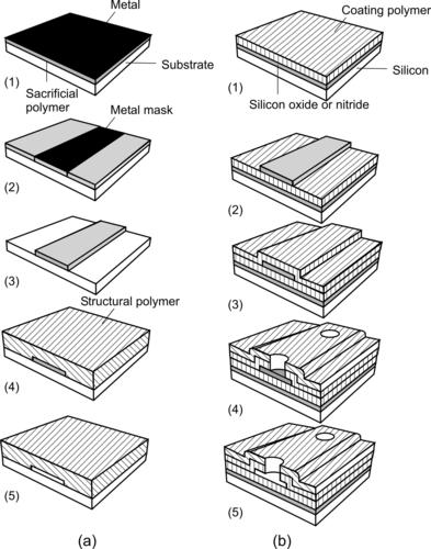 |
| FIGURE 4.19 Fabrication of microchannel with polymeric surface micromachining: (a) a simple channel (after [77]); (b) microchannel with functional coating of inner wall. (after [85]) |
In the above-mentioned process, the sacrificial polymer should easily decompose at a temperature lower than the glass temperature of wall materials. For instance, polynorbornene (PNB) is a good sacrificial polymer [78]. The decomposition temperatures of PNB are between 370°C and 425°C. In this case, silicon dioxide and silicon nitride are ideal encapsulation materials at these relatively high temperatures. If polymeric channel walls are needed, polyimides, such as Amoco Ultradel 7501, Dupont PI-2611, and Dupont PI-2734, are ideal for this purpose, because of their high glass transition temperature of over 400°C [78].
Polycarbonates, such as polyethylene carbonate (PEC) and polypropylene carbonate (PPC), offer relatively low decomposition temperature on the order of 200–300°C [77]. The low decomposition temperature is needed for structural materials with less thermal stability. Inorganic glass, silicon dioxide, thermoplastic polymers, and thermoset polymers can be used as structural materials [77].
Micromixers used in life sciences may need a biocompatible coating for their inner walls. Fig. 3.19 (b) shows the fabrication processes of such microchannels [85]. For instance, the biocompatible material can be parylene C. First, parylene is vapor-deposited on a silicon substrate, which is covered by a nitride/oxide barrier layer (Fig. 4.19 (b,1)). Thick-film resist AZ4620 is used as the sacrificial material. After photolithography, developing, and hard bake of the resist structures (Figs. 4.19 (b,2)), a second parylene layer is deposited (Figs. 3.19 (b,3)). After roughening the parylene surface with oxygen plasma, photosensitive polyimide is spin-coated as a structural layer on top of the second parylene layer. Next, polyimide is exposed and developed. In order to open the fluidic access from the front side, the top parylene layer is etched in oxygen plasma with an aluminum mask (Fig. 4.19 (b,4)). In the last step, the sacrificial layer is removed with acetone. The resulting microchannels are optically transparent and hermetic (Fig. 4.19 (b,5)).
4.3. Metallic Microtechnologies
4.3.1. Metals as substrate materials
Metals are compatible to silicon-based processes, thus metallic micromixers can be fabricated with conventional photolithography. In general, a silicon oxide layer or even the silicon wafer substrate can work as the sacrificial layer. The metallic layer can be evaporated, sputtered, or electroplated on the sacrificial material. Due to the relatively slow growth rate, evaporation and sputtering are suitable for the deposition of thin metallic films up to 10-μm thickness. Thicker metallic layer can be achieved by electroplating. A metallic layer can be patterned by a lift-off process or by chemical etching. Subsequently, etching away the sacrificial materials releases the freestanding metallic structure.
Actuators are the key components of active micromixers. Sputtering and metallic micromachining allow the design and integration of functional smart materials, such as permanent magnet films [88] and [89], piezoelectric films [90] and [91] and shape memory alloy films [92].
Micromagnets consisting of metal alloys such as SmCo5, Sm2(Co, Fe, Zr)17, Nd2Fe17, Nd(Fe, Ti)12Nx, PtCo/Ag, Pt/Fe, CoNiMnP, FeCrCo, and MnAl can be sputtered or electroplated on the substrate. Further, magnetic powders, such as ferrite (Fe2O3), can be mixed with a polymer, such as polyimide or PDMS, to form a magnetic polymeric matrix. This magnetic polymer matrix can be structured by the common polymeric techniques discussed above or screen-printed on a substrate [88]. Magnetic materials open up potential applications in magnetic micromixers and MHD micromixers.
Piezoelectric thin films are not metallic but belong to the class of smart materials for actuation in active micromixers [90]. Piezoelectric ceramics, such as AlN and ZnO, can be sputtered. While ZnO needs to be deposited at room temperature for high resistivity, AlN with low conductivity can be deposited at high temperatures between 100°C and 900°C. AlN is more compatible to silicon-based technology because of the large resistivity and large band gap of 6eV. Other popular piezoelectric materials for MEMS devices are ferroelectric thin films, such as lead zirconate titanate (PZT). Ferroelectric thin films have the advantage of large piezoelectric coefficients. However, for the composition of the material the deposition process is relatively complex and challenging [90]. Readers may refer to a recent review by Doerey and Whatmore for more details on fabrication issues of thick-film PZT [91].
Shape memory alloy (SMA) films are another attractive metallic material for actuators in active micromixers. SMA materials, such as TiNi, can be sputtered and structured with conventional microtechniques. The main advantages of SMA are high power density, large displacement and large forces, and relatively low operation voltages. However, SMA actuators are thermal actuators that are associated with problems such as low energy efficiency, low dynamics, and large hysteresis. The hysteresis behavior leads to nonlinear system behavior, which makes designing SMA-based micro-actuators difficult. A number of microfluidic devices, such as micropumps and microvalves, have been realized based on SMA thin films [92].
4.3.2. LIGA
LIGA process is a combination of X-ray or thick-resist lithography with electroplating. The metallic part usually works as the mold for further replication in polymers. However, the same process can be used for the fabrication of metallic micromixers. The process starts with applying a PMMA layer on the substrate. This process can be achieved by different methods, such as multiple spin coating, lamination of prefabricated sheets, casting, and plasma polymerization. The PMMA layer is structured by X-ray lithography. The etched PMMA part is subsequently used as a mold for electroplating of the metallic structure. The metal in use is typically nickel or nickel–iron alloy.
The need of synchrotron X-ray source and the consequent high cost prevent the widespread use of the LIGA process. The relatively high aspect ratio achievable with SU-8 allows a low-cost alternative to standard LIGA. The LIGA process with SU-8 is often called UV-LIGA or “poor man’s LIGA”[93]. For more details on LIGA technology and its application, readers may refer to a recent review by Malek and Saile [94].
4.3.3. Micro-electro-discharge machining
Micro-electro-discharge machining (micro-EDM) uses erosive effects of electrostatic discharge between an electrode and an electrically conducting material. The electrostatic discharge can create locally a temperature up to 10,000°C. Both electrode and substrate material are immersed in a dielectric fluid that also cools and removes debris from the processed location [95]. The electrode can be machined with conventional techniques. Electropolishing usually follows EDM to both improve the surface finish and remove the heat-affected zone.
An alternative for EDM is electro-chemical machining (ECM) [96]. This technique is based on the electrochemical reaction between an electrode and a workpiece. The advantages of ECM are the low mechanical stress and nonexistence of heat-affected zone as well as tool wear. The technique utilizing both electro-discharge and chemical reaction for machining nonconducting materials is called spark-assisted chemical engraving (SACE). In this technique, the substrate material does not work as an electrode. The external tool electrode and counter-electrode work as the cathode and the anode, respectively. The tool electrode is placed on the substrate surface and submerged in an electrolyte solution (typically, sodium hydroxide or potassium hydroxide). At first, gas bubbles are generated at the tool electrode due to electrolysis. If the voltage between the two electrodes is higher than a critical value, the gas bubbles coalesce into a gas film isolating the tool electrode from the electrolyte. At this moment, electrical discharges occur. The high temperature and probably chemical etching contribute to the eroding of the nonconducting substrate placed next to the electrode. More details about SACE are given in the recent review by Wüthrich and Fascio [97].
4.3.4. Focused ion beam micromachining
Focused ion beam (FIB) micromachining uses highly focused ion beams such as Ga+ beam to scan and cut the substrate surface inside a vacuum chamber. This technique was originally developed for sample preparation in electron microscopy. The spot size of FIB is less than 10nm. The removal rates can further be improved by introducing reactive halogen gases into the processing chamber. Several effects result from the ion bombardment. First, neutral and ionized atoms are removed from the substrate, enabling micromachining of the substrate. The bombardment results in electron emission, which also allows imaging of the sample. Furthermore, the ion beam can induce damages due to the displacement of atoms and heating in the substrate. Chemical interactions, such as breaking of chemical bonds, can be used for deposition. For more details on concepts and applications of FIB micromachining, readers may refer to the recent review by Reyntjens and Puers [98].
4.3.5. Powder blasting
Powder blasting is an erosion technique that uses kinetic energy of powder particles to generate cracks on the substrate surface and consequently to remove material. The major process parameters of this technique are particle material, particle size, particle velocity, and incident angle [101]. The technique was originally developed for metals and further extended to silicon and glass. The main advantage of powder blasting is the fast processing time. Because of this reason, the ink supply channels of inkjet print head are machined by powder blasting.
The resolution of powder blasting depends on the particle size. As a rule of thumb, the smallest cut is about three times that of the particle size [102]. High resolutions are kept by the use of a hard metal mask, which is machined by another technique, such as laser micromachining. Alternatively, masks made of thick-resist foils and polyimide resist can also be used [102]. With particle velocities on the order of 80–200m/s, the erosion rate is on the order of 1mm/min [101].
Using 30-μm alumina particles, microchannels of 100-μm width and 10-μm depth were fabricated in glass [101]. Changing the incident angle of the powder beam can lead to channels with slanted walls. Since glass has a relatively high zeta potential, powder blasting can be the economic way for mass fabrication of active micromixers based on electrokinetic instability. Shlautmann et al. fabricated microchannels with 85-μm width and 22-μm depth in glass using 9-μm alumina particles [103]. In the fabrication of micromixers, powder blasting can be used for drilling fluidic access through a substrate.
4.3.6. Ultrasonic micromachining
Another practical technique for cutting microchannels and opening access holes is ultrasonic drilling. This technique uses ultrasonically induced vibrations delivered to a tool to machine the substrate. When combined with abrasive slurry, ultrasonic abrasion can handle hard, brittle materials, such as glass and silicon.
High-frequency electrical signal is converted through a piezoelectric transducer into mechanical oscillation. The energy is acoustically transmitted to the machining tool. A piezoelectric stack actuator can work as the piezoelectric transducer. The actuation frequency is typically 20kHz. Abrasive slurry flows around the cutting tool and causes microscopic grinding between the surfaces of the tool and the workpiece. Through this process, the machined area becomes an exact counterpart of the tool. In the fabrication process of micromixers, ultrasonic machining can be used for drilling access holes in glass and silicon. Hole diameters on the order of 100–200μm can be machined with this method.
4.4. Packaging
4.4.1. Anodic bonding
Anodic bonding is the oldest bonding technique in silicon-based micromachining. The technique is applied to a glass wafer and a silicon wafer. The required conditions for the process are the bonding temperature on the order of 400°C and the high electrical field with bonding voltage about 1kV. Figure 3.20 describes the typical setup of anodic bonding. Silicon is connected to the positive electrode and works as an anode, which gives the name to this bonding technique.
Anodic bonding induces a large temperature change to the glass/silicon stack. If the thermal expansion coefficients of glass and silicon do not match, the stress upon cooling will cause cracks in either silicon or glass. Thus, the glass wafer should have matching thermal expansion coefficient. Glasses suitable for this purpose are Corning 7740 (Pyrex), Corning 7750, Schott 8329, and Schott 8330. Bonding between two silicon layers can also be achieved with anodic bonding by coating a thin glass layer on one of the two wafers. The glass layer can be deposited by different techniques, such as PVD and spin-on glass. Glass material with a matching thermal expansion coefficient is used as a source or target for the evaporation or sputtering process. The bonding processes work as usual with the glass-covered silicon wafer replacing the glass wafer in Fig. 4.20. Because of the much thinner glass layer on the order of 0.5–4μm, much lower bonding voltages are needed for the same field strength of bonding glass to silicon. The bonding voltage in this case is on the order of several tens of volts. A thin metal layer on glass or silicon does not affect the bonding quality. Electric interconnects can therefore survive the bonding process. Because of the optically transparent glass, this bonding technique is suitable for making micromixers for biochemical applications, where optical access for manipulation and evaluation of the fluid are required.
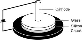
4.4.2. Direct bonding
Direct bonding refers to the bonding process between two substrates of the same material. Direct bonding applies to a variety of materials such as silicon, glasses, polymers, ceramics, and metals.
Silicon direct bonding, also called silicon fusion bonding, seals two silicon wafers directly under high temperature. An intermediate layer makes the fabrication process more complex and more complicated. The advantage of this technique is the lack of thermal stress because of the perfectly matching thermal expansion coefficient of the two silicon wafers. Silicon direct bonding utilizes the reaction between hydroxyl (OH) groups at the surface of the oxide layers of the two silicon wafers. These oxide layers can be either native or deposited. Hydration of the silicon wafers is achieved by immersing them in an H2O2/H2SO4 mixture, boiling nitric acid, or diluted H2SO4. The bonding process is carried out at temperatures between 300°C and 1000°C. Annealing the bonded stack at high temperatures (800°C to 1100°C) further improves the bond quality.
Because of the optical transparency, glasses are relevant for many micromixers for life-science applications. Bonding between glasses is called glass–glass bonding. Many applications use soda-lime glass, which consists of SiO2, Na2O, CaO, MgO, and a small amount of Al2O3. The following bonding process is used for two soda-lime glass slides. First, the glass wafers are cleaned in an ultrasonic bath and subsequently 10minutes in a solution of [5 H2O: 1 NH3 (25%): 1 H2O2 (20%)] or [6H2O: 1 HCl (37%): 1 H2O2 (20%)]. After removing moisture by annealing at 130°C, the two wafers are thermally bonded together at 600°C for 6–8h [104].
Many polymers are thermally bonded at temperatures above their glass transition temperatures. In cases of polymers with low surface energy, such as PDMS, a surface treatment with oxygen plasma seals the two polymer parts at room temperature. Polymer–polymer bonding can be achieved with the assistance of a solvent, which wets the bonding surfaces. Bonding is accomplished after the solvent evaporates.
4.4.3. Adhesive bonding
Adhesive bonding uses an intermediate layer to “glue” the substrate. Depending on substrate materials and applications, the intermediate layer can be glass, epoxies, photoresists, or other polymers. A thin intermediate glass layer can thermally bond silicon wafers. Glass frits with relatively low sealing temperatures ranging from 400°C to 650°C are commercially available. The glass layer can be sprayed, screen-printed, or sputtered on the substrate. Annealing the stack at sealing temperatures makes the glass layer melt and flow. Cooling down to room temperature results in a strong bond between two substrates [107]. A number of epoxies [108], UV-curable epoxies [109] and photoresists can be used for adhesive bonding. SU-8 is used in many microfluidic applications as both spacer and adhesive layers. The advantage of using polymers as an intermediate layer is the low process temperature. These low packaging temperatures are needed for many devices, which have metals and alloys with low melting temperatures. The other advantage is that adhesive bonding is not limited to silicon and can be used for all types of substrate material.
4.4.4. Eutectic bonding
Eutectic bonding is a common packaging technique in electronics. Gold–silicon eutectic bonding is achieved at a relatively low temperature of 363°C. A thin gold film can be sputtered on the silicon surface for this purpose. Furthermore, a gold–silicon preform with composition close to the eutectic point can also be used as the intermediate layer.
4.5. Conclusions
This chapter gives a short review on available micromachining technologies for silicon-based, metallic, and polymeric micromixers. Because a complete review on the technology for each type of material could cover hundreds of references, this chapter only summarizes the most important points on the topics, and in many cases cites the topical review on each type of material. In general, silicon-based technologies are the most established techniques with commercially available equipments. Applications in rough environments and operation conditions require a tougher material than silicon. For such applications, diamond-based and silicon carbide-based devices are the better candidates. Applications in analytical chemistry and biomedical fields would require a large device area, which is not economical for silicon. Furthermore, silicon and silicon-based materials are not compatible for many chemical and biochemical applications. Polymeric devices are the real alternatives for silicon-based counterparts. Besides simple devices with only microchannel networks, polymeric devices with freely movable components are also possible. Metallic devices are other alternatives in microscale. The combination of all the available technologies from silicon-based to polymeric to metallic opens an enormous potential and freedom for designing micromixers.
References
[1] Madou, M.J., Fundamentals of Microfabrication: The Science of Miniaturization. 2nd ed (2002) CRC Press, Boca Raton, FL.
[2] Thompson, L.F.; Willson, C.G.; Bowden, M.J., Introduction to Microlithography. (1994) American Chemical Society, Washington, D.C.
[3] Friedrich, H.; Widmann, D.; Mader, H., Technologie Hochintegrierter Schaltungen. (1996) Springer-Verlag, Berlin.
[4] Adams, A.C., Dielectric and polysilicon film deposition, In: (Editor: Sze, S.M.) VLSI Technology (1988) McGraw-Hill, New York, pp. 233–271.
[5] Monreal, G.; Mari, C.M., The use of polymer materials as sensitive elements in physical and chemical sensors, J. Micromech. Microeng. 7 (3) (1997) 121–124.
[6] In: (Editor: Soane, D.) Polymer Applications for Biotechnology: Macromolecular Separation and Identification (1992) Prentice-Hall, Upper Saddle River, NJ.
[7] G.T.A. Kovacs, N.I. Maluf, K.E. Petersen, Bulk micromachining of silicon, in: Proceedings of the IEEE, vol. 86, 8, 1998, pp. 1536–1551.
[8] Williams, K.R.; Muller, R.S., Etch rates for micromachining processing, J. Microelectromech. Syst. 5 (4) (1996) 256–269.
[9] Bean, K.E.; Csepregi, L.; Heuberger, A.; Baumgartel, H., Anisotropic etching of crystalline silicon in alkaline solutions II: Influence of dopants, J. Electrochem. Soc. 137 (11) (1990) 3626–3632.
[10] Kaminsky, G., Micromachining of silicon mechanical structures, J. Vac. Sci. Tech. B3 (4) (1985) 1015–1024.
[11] Kern, W., Chemical etching of silicon, germanium, gallium arsenide and gallium phosphide, RCA Review 39 (1978) 278–308.
[12] Schnakenberg, U.; Benecke, W.; Löchel, B.; Ullerich, S.; Lange, P., NH4OH Based etchants for silicon micromachining: influence of additives and stability of passivation layers, Sens. Actuators A Phys. 25 (1–3) (1990) 1–7.
[13] Tabata, O.; Asahi, H.; Funabashi, H.; Shimaoka, K.; Sugiyama, S., Anisotropic etching of silicon in TMAH solutions, Sens. Actuators A Phys. 34 (1) (1992) 51–57.
[14] U. Schnakenberg, W. Beneke, P. Lange, TMAHW etchants for silicon micromachining, in: Proceedings of Transducers ‘91, 6th International Conference on Solid-State Sensors and Actuators, San Francisco, 23–27 June, 1991, pp. 815–818.
[15] K.E. Petersen, Silicon as a mechanical material, in: Proceedings of IEEE, vol. 70, 1982, pp. 420–457.
[16] Mehregany, M.; Senturia, S.D., Anisotropic etching of silicon in hydrazine, Sens. Actuators A Phys. 13 (4) (1988) 375–390.
[17] Linde, H.; Austin, L., Wet silicon etching with aqueous amine gallates, J. Electrochem. Soc. 139 (4) (1992) 1170–1174.
[18] V. Lehmann, Porous silicon—A new material for MEMS, Proceedings of MEMS ‘96, 9th IEEE international workshop micro electromechanical system, San Diego, CA, 11–15 February, 1996, pp. 1–6.
[19] P. Lärmer, Method of Anisotropically Etching Silicon, German Patent DE 4 241 045, 1994.
[20] D. Sobek, S.D. Senturia and M.L. Gray, Microfabricated Fused Silica Flow Chambers for Flow Cytometry, Technical digest of the IEEE solid state sensor and actuator workshop, Hilton Head Island, SC, 13–16 June, 1994, pp. 260–263.
[21] Harrison, D.J.; Fluri, K.; Seiler, K.; Fan, Z.H.; Effenhauser, C.S.; Manz, A., Micromachining a miniaturized capillary electrophoresis-based chemical-analysis system on a chip, Science 261 (1993) 895–897.
[22] Jacobson, S.C.; Hergenroder, R.; Kountry, L.B.; Ramsey, J.M., High-speed separations on a microchip, Analytical Chemistry 66 (1994) 1114–1118.
[23] Ehrfeld, W.; Hessel, V.; Mobius, H.; Richter, T.; Russow, K., Potentials and realization of microreactors, microsystem technology for chemical and biological microreactors, Dechema monographs 132 (1996) 1–28.
[24] L. Jiang, M. Wong and Y. Zohar, A Micro-Channel Heat Sink with Integrated Temperature Sensors for Phase Transition Study, in: Proceedings of MEMS ‘99, 12th IEEE international workshop micro electromechanical system, Orlando, FL, 17–21 January, 1999, pp. 159–164.
[25] Chen, J.; Wise, K.D., A high resolution silicon monolithic nozzle array for inkjet printing, IEEE Transaction on Electron Devices 44 (9) (1997) 1401–1409.
[26] Chen, J.; Wise, K.D.; Hetke, J.F.; Bledsoe, S.C., A multichannel neural probe for selective chemical delivery at the cellular level, IEEE Transaction on Biomedical Engineering 44 (8) (1997) 760–769.
[27] R.W. Tjerkstra, M. de Boer, E. Berenschot, J.G.E. Gardeniers, A. van den Berg, K. Elwenspoek, Etching technology for microchannels, in: Proceedings of MEMS ‘97, 10th IEEE international workshop micro electromechanical system, Nagoya, Japan, 26–30 January, 1997, pp. 147–151.
[28] de Boer, M.J.; Tjerkstra, R.W.; Berenschot, J.W.; Jansen, M.V.; Burger, C.J.; Gardenter, J.G.E.; Elwenspoek, M.; van den Berg, A., Micromachining of buried micro channels in silicon, J. Microelectromech. Syst. 9 (1) (2000) 94–103.
[29] L. Lin, A.P. Pisano and R.S. Muller, Silicon processed microneedles, in: Proceedings of transducers ‘93, 7th international conference on solid-state sensors and actuators, Yokohama, Japan, 7–10 June, 1993, pp. 237–240.
[30] S. Wu, J. Mai, Y. Zohar, Y.C. Tai, C.M. Ho, A suspended microchannel with integrated temperature sensors for high-pressure flow studies, in: Proceedings of MEMS ‘98, 11th IEEE international workshop micro electromechanical system, Heidelberg, Germany, 25–29 January, 1998, pp. 87–92.
[31] V.L. Spiering, J.N. van der Moolen, G.J. Burer, A. van den Berg, Novel microstructures and technologies applied in chemical analysis techniques, in: Proceedings of transducers ‘97, 9th international conference on solid-state sensors and actuators, Chicago, IL, 16–19 June, 1997, pp. 511–514.
[32] Papautsky, I.; Brazzle, J.; Swerdlow, H.; Weiss, R.; Frazier, F.B., Micromachined pipette arrays, IEEE Transaction on Biomedical Engineering 47 (6) (2000) 812–819.
[33] E.T. Carlen and C.H. Mastrangelo, Paraffin actuated surface micromachined valves, in: Proceedings of MEMS ‘00, 13th IEEE international workshop micro electromechanical system, Miyazaci, Japan, 23–27 January, 2000, pp. 381–385.
[34] Auciello, O.; Birrell, J.; Carlisle, J.A.; Gerbi, J.E.; Xiao, X.; Peng, B.; Espinosa, H.D., Materials science and fabrication processes for a new MEMS technology based on ultrananocrystalline diamond thin films, J. Phys. Condens. Mat. 16 (2004) R539–R552.
[35] Gurbuz, Y.; Esame, O.; Tekin, I.; Kang, W.P.; Davidson, J.L., Diamond semiconductor technology for RF device applications, Solid-State Electron. 49 (2005) 1055–1070.
[36] Mehregany, M.; Zorman, C.A.; Roy, S.; Flischman, A.J.; Wu, C.H.; Rajan, N., Silicon carbide for microelectromechanical systems, International Materials Reviews 45 (2000) 85–108.
[37] Okojie, R.S.; Ned, A.A.; Kurtz, A.D., Operation of (6H)-SiC pressure sensor at 500°C, Sens. Actuators A Phys. 66 (1998) 200–204.
[38] Rajan, N.; Mehregany, M.; Zorman, C.A.; Stefanescu, S.; Kicher, T.P., Fabrication and testing of micromachined silicon carbide and nickel fuel atomizers for gas turbine engines, J. Microelectromech. Syst. 8 (1999) 251–257.
[39] Kotzar, G.; Freas, M.; Abel, P.; Fleischman, A.; Roy, S.; Zorman, C.; Moran, J.M.; Melzak, J., Evaluation of MEMS materials of construction for implantable medical device, Biomaterials 23 (2002) 2737–2750.
[40] Voskerician, G.; Shive, M.S.; Shawgo, R.S.; von Recum, H.; Anderson, J.M.; Cima, M.J.; Langer, R., Biocompatability and biofouling of MEMS drug delivery device, Biomaterials 24 (2003) 1959–1967.
[41] Hernandez, P.R.; Taboada, C.; Leijia, L.; Tsutsumi, V.; Vazquez, B.; Valdes-Perezgasga, F.; Reyes, J.L., Evaluation of biocompatibility of pH-ISFET materials during long-term subcutaneous implantation, Sens. Actuators B Chem. 46 (1998) 133–138.
[42] A.C.R. Grayson, R.S. Shawgo, A.M. Johnson, N.T. Flynn, Y. Li, M.J. Cima and R.A. Langer, BioMEMS review: MEMS technology for physiologically integrated devices, in: Proceedings of the IEEE, vol. 92, 2004, pp. 6–21.
[43] Ziaie, B.; Baldi, A.; Lei, M.; Gu, Y.; Sigel, R.A., Hard and soft micromachining for BioMEMS: review of techniques and examples of application in microfluidics and drug delivery, Adv. Drug Deliv. Rev. 56 (2004) 145–172.
[44] Whitesides, G.M.; Ostuni, E.; Takayama, S.; Jiang, X.; Ingber, D.E., Soft lithography in biology and biochemistry, Annu. Rev. Biomed. Eng. 3 (2001) 335–373.
[45] Lendlein, A.; Kelch, S., Shape memory polymers, Angew. Chem. Int. Ed. 41 (2002) 2034–2057.
[46] Facchetti, A.; Yoon, M.H.; Marks, T.J., Gate dielectrics for organic field-effect transistor: new opportunities for organic electronics, Adv. Mater. 17 (2005) 1705–1725.
[47] E.W. Becker, W. Ehrfeld, P. Hagmann, A. Maner, D. Munchmeyer, Fabrication of microstructures with high aspect ratios and great structural heights by synchrotron radiation lithography, glavanoforming, and plastic moulding (LIGA Process), Microelectron. Eng. 4, pp. 35–56.
[48] H. Guckel, T.R. Christensen and K.J. Skrobis, Formation of Microstructures Using a Preformed Photoresist Sheet, U.S. Patent #5378583, January 1995.
[49] Chaudhuri, B.; Guckel, H.; Klein, J.; Fisher, K., Photoresist application for the LIGA process, Microsystem Technologies 4 (1998) 159–162.
[50] Mohr, J.; Ehrfeld, W.; Munchmeyer, D., Requirements on resist layers in deep-etch synchrotron radiation lithography, J. Vac. Sci. Tech. B6 (1988) 2264–2267.
[51] H. Guckel, J. Uglow, M. Lin, D. Denton, J. Tobin, K. Euch, M. Juda, Plasma polymerization of methyl methacrylate: A photoresist for 3D applications, Technical Digest of the IEEE Solid State Sensor and Actuator Workshop, Hilton Head Island, SC, 4–7 June, 1988, pp. 43–46.
[52] V. Ghica and W. Glashauser, Verfahren für die Spannungsfreie Entwicklung von Bestrahlten Polymethylmethacrylate-Schichten, German patent, #3039110, 1982.
[53] Shaw, J.M.; Gelorme, J.D.; la Bianca, N.C.; Renaud, P.; Vettiger, P., Negative photoresists for optical lithography, IBM Journal of Research and Development 41 (1997) 81–94.
[54] Lorenz, H.; Despont, M.; Fahrni, N.; la Bianca, N.; Renaund, P.; Vettinger, P., SU-8: A low-cost negative resist for MEMS, J. Micromech. Microeng. 7 (1997) 121–124.
[55] Lorenz, H.; Vettinger, P.; Renaud, P., Fabrication of photoplastic high-aspect ratio microparts and micromolds using SU-8 UV resist, Microsystem Technologies 4 (1998) 143–146.
[56] MicroChem Corp, NANO™SU-8 Negative Tone Photoresists Formulations 2–25, Data sheets, 2001.
[57] MicroChem Corp, NANO™SU-8 Negative Tone Photoresists Formulations 50–100, Data sheets, 2001.
[58] Chang, H.K.; Kim, Y.K., UV-LIGA process for high aspect ratio structure using stress barrier and C-shaped etch hole, Sens. Actuators A Phys. 84 (2000) 342–350.
[59] Ghantasala, M.K.; Hayes, J.P.; Harvey, E.C.; Sood, D.K., Patterning, electroplating and removal of SU-8 moulds by excimer laser micromachining, J. Micromech. Microeng. 11 (2001) 133–139.
[60] Ayliffe, H.E.; Frazier, A.B.; Rabbitt, R.D., Electric impedance spectroscopy using microchannels with integrated metal electrodes, IEEE J. Microelectromech. Syst. Vol.8 (1) (1999) 50–57.
[61] Jackman, R.J.; Floyd, T.M.; Ghodssi, R.; Schmidt, M.A.; Jensen, J.F., Microfluidic systems with on-line UV detection fabricated in photodefinable epoxy, J. Micromech. Microeng. 11 (2001) 263–269.
[62] Alderman, B.E.J.; Mann, C.M.; Steenson, D.P.; Chamberlain, J.M., Microfabrication of channels using an embedded mask in negative resist, J. Micromech. Microeng. 11 (2001) 703–705.
[63] L.J. Guerin, M. Bossel, M. Demierre, S. Calmes, Ph. Renaud, Simple and low cost fabrication of embedded micro channels by using a new thick-film photoplastic, Proceedings of transducers ‘97, 9th international conference on solid-state sensors and actuators, Chicago, IL, 16–19 June, 1997, pp. 1419–1421.
[64] Chuang, Y.J.; Tseng, F.G.; Cheng, J.H.; Lin, W.K., A novel fabrication method of embedded micro-channels by using SU-8 thick-film photoresists, Sens. Actuators A Phys. 103 (2003) 64–69.
[65] Tay, F.E.H.; van Kan, J.A.; Watt, F.; Cheong, W.O.; et al., A novel micro-machining method for the fabrication of thick-film SU-8 embedded micro-channels, J. Micromech. Microeng. 11 (2001) 27–32.
[66] O’Brien, J.; Hughes, P.J.; Bunnet, M.; O’Neill, B.; Alderman, J.; Lane, B.; O’Riordan, A.; O’Driscoll, C., Advanced photoresist technologies for microsystems, J. Micromech. Microeng. 11 (2001) 353–358.
[67] Qu, W.; Wenzel, C.; Jahn, A., One-mask procedure for the fabrication of movable high-aspect-ratio 3D microstructures, J. Micromech. Microeng. 8 (1998) 279–283.
[68] Conédéra, V.; Le Goff, B.; Fabre, N., Potentialities of a new positive photoresist for the realization of thick moulds, J. Micromech. Microeng. 9 (1999) 173–175.
[69] Loechel, B., Thick-layer resists for surface micromachining, J. Micromech. Microeng. 10 (2000) 108–115.
[70] Zhao, Y.; Cui, T., Fabrication of high-aspect-ratio polymer-based electrostatic comb drives using the hot embossing technique, J. Micromech. Microeng. 13 (2003) 430–435.
[71] Truong, T.Q.; Nguyen, N.T., A polymeric piezoelectric micropump based on lamination technology, J. Micromech. Microeng. 14 (2004) 632–638.
[72] Nguyen, N.T.; Ho, S.S.; Low, L.N., A polymeric microgripper with integrated thermal actuators, J. Micromech. Microeng. 14 (2004) 969–974.
[73] Frazier, A.B.; Allen, M.G., Metallic microstructures fabricated using photosensitive polyimide electroplating molds, J. Microelectromech. Syst. 2 (2) (1993) 87–94.
[74] Ito, T.; Sawada, R.; Higurashi, E.; Kiyokura, T., Fabrication of microstructure using fluorinated polyimide and silicon-based positive photoresist, Microsystem Technologies 6 (2000) 165–168.
[75] Stieglitz, T., Flexible biomedical microdevices with double-sided electrode arrangements for neural applications, Sens. Actuators A Phys. 90 (2001) 203–211.
[76] Metz, S.; Holzer, R.; Renaud, P., Polyimide-based microfluidic devices, Lab on a Chip 1 (1) (2001) 29–34.
[77] Reed, H.A.; White, G.E.; Rao, V.; Allen, S.A.B.; Henderson, C.L.; Kohl, P.A., Fabrication of microchannels using polycarbonates as sacrificial materials, J. Micromech. Microeng. 11 (2001) 733–737.
[78] Bhusari, D.; Reed, H.A.; Wedlake, M.; Padovani, A.M.; Allen, S.A.B.; Kohl, P.A., Fabrication of air-channel structures for microfluidic, microelectromechanical, and microelectronic applications, J. Micromech. Microeng. 10 (2001) 400–408.
[79] Piotter, V.; Hanemann, T.; Ruprecht, R.; Haupelt, J., Injection molding and related techniques for fabrication of microstructures, Microsystem Technologies 4 (1997) 129–133.
[80] O. Larsson, O. Ohman, A. Billman, L. Lundbladh, C. Lindell, G. Palmskog, Silicon based replication technology of 3D-microstructures by conventional cd-injection molding techniques, in: Proceedings of transducers ‘97, 9th international conference on solid-state sensors and actuators, Chicago, IL, 16–19 June, 1997, pp. 1415–1418.
[81] Niggemann, M.; Ehrfeld, W.; Weber, L.; Gunther, R.; Sollbohmer, O., Miniaturized plastic micro plates for applications in HTS, Microsystem Technologies 6 (1999) 48–53.
[82] Gerlach, A.; Keller, W.; Schulz, J.; Schumacher, K., Gas permeability of adhesives and their application for hermetic packaging of microcomponents, Microsystem Technologies 7 (2001) 17–22.
[83] Becker, H.; Heim, U., Hot embossing as a method for the fabrication of polymer high aspect ratio structures, Sens. Actuators A Phys. 83 (2000) 130–135.
[84] Heckele, M.; Bacher, W.; Müller, K.D., Hot embossing—the molding technique for plastic microstructures, Microsystem Technologies 4 (1998) 122–124.
[85] P.F. Man, D.K. Jones and C.H. Mastrangelo, Microfluidic plastic capillaries on silicon substrates: A new inexpensive technology for bioanalysis chips, in: Proceedings of MEMS ‘97, 10th IEEE international workshop micro electromechanical system, Nagoya, Japan, 26–30 January, 1997, pp. 311–316.
[86] Xia, Y.; Whitesides, G.M., Soft lithography, Ann. Review of Material Sciences 28 (1998) 153–194.
[87] Duffy, D.C.; McDonald, J.C.; Schuller, O.J.A.; Whitesides, G.M., Rapid prototyping of microfluidic switches in poly (dimethyl Siloxane) and their actuation by electro-osmotic flow, J. Micromech. Microeng. 9 (1999) 211–217.
[88] Chin, T.S., Permanent magnet films for applications in microelectromechanical systems, J. Magn. Magn. Mat. 209 (2000) 75–79.
[89] Gibbs, M.R.J., Applications of magMEMS, J. Magn. Magn. Mater. 290–291 (2005) 1298–1303.
[90] Trolier-McKinstry, S.; Muralt, P., Thin film piezoelectrics for MEMS, J. Electroceramics 12 (2004) 7–17.
[91] Dorey, R.A.; Whatmore, R.W., Electroceramic thick film fabrication for MEMS, J. Electroceramics 12 (2004) 19–32.
[92] Fu, Y.; Du, H.; Huang, W.; Zhang, S.; Hui, M., TiNi-based thin films in MEMS applications: a review, Sens. Actuators A Phys. 112 (2004) 395–408.
[93] Lee, K.Y.; Labianca, N.; Rishton, S.A.; Zolgharnain, S.; Gelorme, J.D.; Shaw, J.; Chang, T.H.P., Micromachining applications of a high resolution ultra-thick photoresist, J. Vac. Sci. Tech. B 13 (1995) 3012–3016.
[94] Malek, C.K.; Saile, V., Applications of LIGA technology to precision manufacturing of high-aspect-ratio micro-components and -systems: a review, Microelectronics J. 35 (2004) 131–143.
[95] Schoth, A.; Förster, R.; Menz, W., Micro wire EDM for high aspect ratio 3D microstructuring of ceramics and metals, Microsystem Technologies 11 (2005) 250–253.
[96] Schuster, R.; Kirchner, V.; Allongue, P.; Ertl, G., Electrochemical micromachining, Science 289 (2000) 98–101.
[97] Wüthrich, R.; Fasciob, V., Machining of non-conducting materials using electrochemical discharge phenomenon-an overview, Int. J. Mach. Tool. Manufact. 45 (2005) 1095–1108.
[98] Reyntjens, S.; Puers, R., A review of focused ion beam applications in microsystem technology, J. Micromech. Microeng. 11 (2001) 287–300.
[99] Chichkov, B.N.; Momma, C.; Note, S.; von Alvensleben, F.; Tunnermann, A., Femtosecond, picosecond and nanosecond laser ablation of solids, Appl. Phys. A 63 (1996) 109–115.
[100] Laws, R.A.; Holmes, A.S.; Goodall, F.N., The formation of moulds for 3D microstructures using excimer laser ablation, Microsystem Technologies 3 (1996) 17–19.
[101] Belloy, E.; Thurre, S.; Walckiers, E.; Sayah, A.; Gijs, M.A.M., The introduction of powder blasting for sensor and microsystem applications, Sens. Actuators A Phys. 84 (2000) 330–337.
[102] Wensink, H.; Jansen, V.H.; Berenschot, J.W.; Elwenspoek, M.C., Mask materials for powder blasting, J. Micromech. Microeng. 10 (2000) 175–180.
[103] Schlaumann, S.; Wensink, H.; Schasfoort, R.; Elwenspoek, M.; van den Berg, A., Powder-blasting technology as an alternative tool for microfabrication of capillary electrophoresis chips with integrated conductivity sensors, J. Micromech. Microeng. 11 (2001) 386–389.
[104] Stjernström, M.; Roeraade, J., Method for fabrication of microfluidic system in glass, J. Micromech. Microeng. 8 (1998) 33–38.
[105] D.W. Matson, P.M. Martin, W.D. Bennett, D.C. Stewart, C.C. Bonham, Laminated ceramic components for micro fluidic applications, in: SPIE Conference Proceeding 3877: microfluidic devices and systems II, Santa Clara, CA, 20–22 September, 1999, pp. 95–100.
[106] P.M. Martin, W.D. Bennett, D.J. Hammerstrom, J.W. Johnston, D.W. Matson, Laser micromachined and laminated microfluidic components for miniaturized thermal, chemical and biological systems, in: SPIE Conference proceedings, 3680: Design, Test, and Microfabrication of MEMS and MOEMS, Paris, France, 30 March–1 April, 1999, pp. 826–833.
[107] Ko, W.H.; Suminto, J.T.; Yeh, G.J., Bonding techniques for microsensors, In: (Editor: Fung, C.D.; et al.) Micromachining and Micropackaging of Transducers (1985) Elsevier, Amsterdam, pp. 41–61.
[108] Weckwerth, M.V.; Simmons, J.A.; Harff, N.E.; Sherwin, M.E.; Blount, M.A.; Baca, W.E.; Chui, H.C., Epoxy bond and stop-etch (EBASE) technique enabling backside processing of (Al)GaAs heterostructures, Superlattice. Microst. 20 (4) (1996) 561–567.
[109] H. Nguyen, P. Patterson, H. Toshiyoshi, M.C. Wu, A substrate-independent wafer transfer technique for surface-micromachined devices, in: Proceedings of MEMS ‘00, 13th IEEE international workshop micro electromechanical system, Miyazaci, Japan, 23–27 January, 2000, pp. 628–632.
..................Content has been hidden....................
You can't read the all page of ebook, please click here login for view all page.