
Chapter 2. The AVR Microcontroller
Because an AVR-based Arduino is really just a physical platform for an AVR microcontroller (i.e., a breakout board), the electrical characteristics of an Arduino are essentially those of the AVR device on the PCB. Understanding the low-level details of an Arduino is really a matter of understanding the AVR device that powers it. To that end, this chapter presents broadly applicable material consisting of high-level descriptions of the main functions utilized in the AVR family. This includes the AVR CPU and the so-called peripheral functions such as timers, counters, serial interface logic, analog-to-digital (A/D) converters, analog comparators, and discrete digital I/O ports.
AVR microcontrollers are available in a wide variety of configurations and package types, which makes writing a chapter like this something of a challenge. Fortunately, the various types of 8-bit AVR devices use a common central processing unit (CPU) and a modular internal architecture built around an internal data bus. This allows for each variant to incorporate different combinations and quantities of functional modules into the AVR’s internal circuitry to meet specific design requirements and support different intended applications.
Due to practical limitations of space, the descriptions in this chapter are necessarily terse and focused on the essential characteristics, and don’t provide may of the low-level details that can be found in the reference documentation available from Atmel. If you need or want to know the logic circuit and register-level details of what’s inside a particular AVR microcontroller, datasheets, user’s guides, and application notes are available from Atmel free of charge.
Background
The AVR microcontroller began life in the early 1990s as a student project at the Norwegian Institute of Technology. Two students, Alf-Egil Bogen and Vegard Wollan, devised an 8-bit device with a RISC-type internal architecture while working at a local semiconductor facility in Trondheim, Norway. The design was later sold to Atmel, where Bogen and Wollan continued to work on it and refine it.
The AVR microcontrollers are highly configurable and very versatile, and they embody several unique features that set them apart from other 8-bit microcontrollers like the 8051 or 68HC05 components. The AVR is a modified Harvard architecture 8-bit RISC microcontroller. In a Harvard architecture read-only program, code and modifiable data (variables) are stored in separate memory spaces. By way of comparison, a microprocessor like the 68040 uses the Von Neumann architecture, in which programs and data share the same memory space.
The AVR family of devices was one of the first to incorporate on-board flash memory for program storage, instead of the one-time programmable ROM (read-only memory), EPROM (erasable programmable read-only memory), or EEPROM (electrically erasable programmable read-only memory) found on other microcontrollers. This makes reprogramming an AVR microcontroller simply a matter of loading new program code into the device’s internal flash memory. Most AVR parts do have a small amount of EEPROM for storing things like operating parameters that must persist between changes in the flash memory.
Internal Architecture
Internally, an AVR ATmega microcontroller consists of an AVR CPU and various input/output, timing, analog-to-digital conversion, counter/timer, and serial interface functions, along with other functions depending on the part number. These are referred to by Atmel as peripheral functions. Besides the I/O functions, the main differences between the AVR microcontroller types lie in the amount of on-board flash memory and available I/O functions. The 8-bit parts all use essentially the same AVR CPU core. The following list shows just some of the basic features of AVR microcontrollers:
-
RISC architecture
-
131 instructions
-
32 8-bit general-purpose registers
-
Up to 20 MHz clock rate (20 MIPS operation)
-
-
On-board memory
-
Flash program memory (up to 256K)
-
On-board EEPROM (up to 4K)
-
Internal SRAM (up to 32K)
-
-
Operating voltage
-
VCC = 1.8 to 5.5V DC
-
Figure 2-1 shows a simplified block diagram of the AVR CPU core found on 8-bit AVR devices. Figure 2-2 shows a generic high-level block diagram of an AVR device. This is not intended to represent any specific AVR device, just an AVR in general.
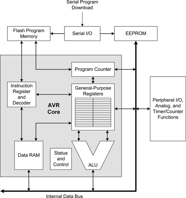
Figure 2-1. AVR CPU block diagram
The peripheral functions are controlled by the CPU via an internal high-speed data bus. Control registers (separate from the CPU registers) are used to configure the operation of the peripherals. All peripheral functions share port pins with the discrete digital I/O capabilities.
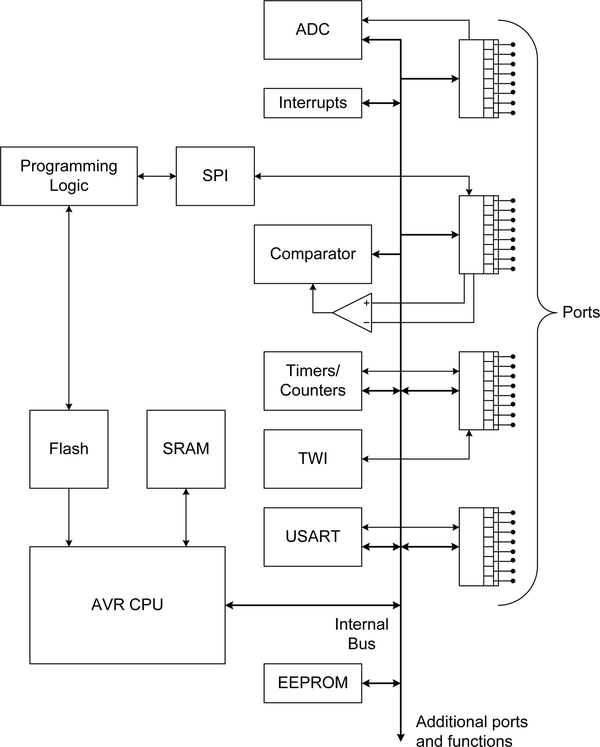
Figure 2-2. Generic AVR microcontroller block diagram
Atmel makes many different types of AVR microcontrollers, which allows hardware designers to pick the part that meets their specific needs and reduce the number of unused pins and wasted space on a printed circuit board. Some, like the tinyAVR parts, come in small surface-mount packages with as few as six pins. Each has one or more discrete digital I/O ports, which can be programmed to perform multiple functions (see “Peripheral Functions”).
For example, the ATTINY13-20SQ comes in an eight-pin DIP (dual in-line pin) or SOIC (small-outline IC) surface-mount package. Six of the device’s pins are connected to an internal 8-bit I/O port (port B). The other two are VCC (power) and ground. The six port B pins can be configured as analog inputs, oscillator outputs, interrupt inputs, SPI signals, or discrete digital inputs or outputs. Internally, the device—even one this small—is still an AVR microcontroller, and it has 1K of built-in flash memory for programs, and 64 bytes of RAM for variables.
On the other end of the spectrum there are AVR parts like the ATmega649, with nine 8-bit ports (A through J, but no I, since I can be confused for the numeral 1), 64K of flash memory, 4K of RAM, 2K of EEPROM, 54 general-purpose I/O pins, and an integrated LCD interface. The AVR32 series of parts are 32-bit AVR processors with up to 256K of flash memory, 32K of RAM, an integrated DSP (digital signal processing) unit, protected memory, and 36 general-purpose I/O pins.
No Arduino boards use an AVR part as small as a tinyAVR (it would be a real challenge to squeeze the Arduino bootloader into something with only 1K of flash and still have room left for a useful program), or anything like the ATmega649 or an AVR32, but the point here is that the AVR family offers many choices, and the parts that have been selected for use in Arduino devices aren’t the only AVR parts that could be used.
Internal Memory
AVR devices all contain various amounts of three types of memory: flash, SRAM (static random-access memory), and EEPROM. The flash memory is used to store program code, the SRAM is used to hold transient data such as program variables and the stack, and the EEPROM can hold data that needs to persist between software changes and power cycles. The flash and EEPROM can be loaded externally, and both will retain their contents when the AVR is powered off. The SRAM is volatile, and its contents will be lost when the AVR loses power.
Peripheral Functions
The heart of an AVR microcontroller is the 8-bit CPU, but what makes it a truly useful microcontroller is the built-in peripheral functions integrated into the IC with the CPU logic. The peripheral functions of an AVR device vary from one type to another. Some have one timer, some have two or more (up to six for some types). Other parts may have a 10-bit A/D converter (ADC), whereas others feature a 12-bit converter. All AVR parts provide bidirectional I/O pins for discrete digital signals. Some versions also support a touchscreen and other types of interactive interfaces.
This section contains general descriptions of the peripheral functions that are used with the various types of AVR devices found in Arduino products, with the ATmega168 serving as a baseline example. This section does not attempt to provide an exhaustive reference for each type of AVR microcontroller, but instead covers the general functionality of each type of peripheral function. Refer to Chapter 3 for specific information regarding the processors used in the Arduino boards described in this book, and also see the Atmel technical documentation for low-level details not provided here.
Control Registers
In addition to 32 general-purpose registers in the CPU, AVR devices also have a number of control registers that determine how the I/O ports, timers, communications interfaces, and other features will behave. The control register set will vary from one type of device to another, since different types may have more or less ports than others, and different peripheral function configurations. The control registers for the AVR parts used in the Arduino boards covered in this book can be found in Appendix B. They are also described in detail in the documentation available directly from Atmel.
Even a modest AVR part like the ATmega168 has far more internal functionality than it has pins available to dedicate to each function. For this reason, most of the pins on an AVR microcontroller can be configured to perform specific functions based on the settings contained in the control registers. Because the pin functions are dynamically configurable, it is possible to have a pin perform one type of function at one point in time, and then perform a different function once the control register value has been modified.
For example, pin 12 of an ATmega168 in a 28-pin DIP package is connected to PD6 (Port D, bit 6), but it can also be configured to act as an interrupt source (PCINT22), as the positive input for the AVR’s internal analog comparator (AIN0), or as the output of a timer comparison logic circuit (the Timer/Counter0 output compare match A), which can be used to generate a PWM (pulse width modulation) signal.
Digital I/O Ports
AVR microcontrollers use bidirectional I/O ports to communicate with the external world. A port is an 8-bit register wherein some or all of the bits are connected to physical pins on the AVR device package. Different types of AVR devices have different numbers of ports, ranging from one for the ATTINY13-20SQ up to nine for the ATmega649. Ports are labeled as A, B, C, and so on.
Each pin of a port is controlled by internal logic that manages the signal direction, the state of an internal pull-up resistor, timing, and other functions. A simplified schematic is shown in Figure 2-3. The Px in Figure 2-3 refers to port bit/pin x (0 through 7). For a detailed description of the AVR port logic, see the AVR technical references.
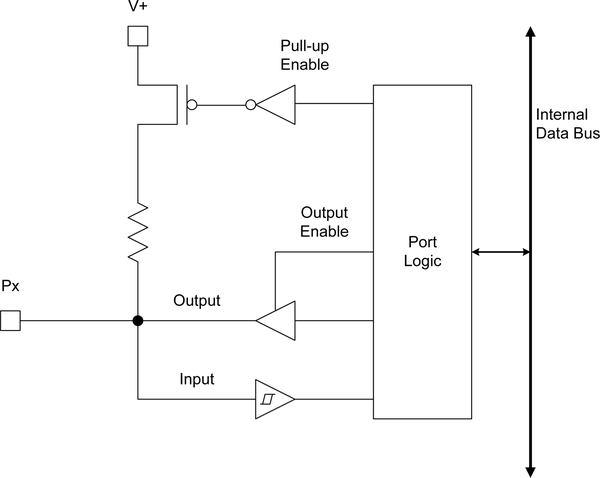
Figure 2-3. AVR I/O port block diagram
Because of the sophisticated logic used to control functionality, an AVR port can perform many different functions—some of them simultaneously. When a port is configured as an output it is still possible to read data from it, and an output can be used to trigger an interrupt (discussed in “Interrupts”).
8-Bit Timer/Counters
There are two forms of 8-bit timer/counter available in AVR microcontrollers. In the first type the clock input is derived from the primary system clock, and hence the timer/counter is synchronous. The second form has the ability to operate in an asynchronous mode using an external clock source. Figure 2-4 shows a simplified schematic of an AVR timer. The control registers for the timer/counter are defined in Appendix B and described in detail in the Atmel technical documentation.
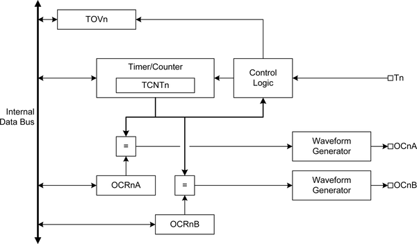
Figure 2-4. AVR timer/counter block diagram
The Timer/Counter0 module in an AVR 8-bit timer/counter peripheral function is a general-purpose timer and/or counter that features two independent output comparison circuits with four modes of operation. The timer/counter modes of operation are as follows:
- Normal mode
-
This is the simplest mode of timer/counter operation. The count always increments and no counter clear is performed when the counter reaches its maximum 8-bit value. When this occurs, the counter overflows and returns to zero. When the counter wraps back to zero, the Timer/Counter Overflow Flag (TOV0) is set. The TOV0 flag can be viewed as a ninth bit, but it is only set, not cleared, by a timer overflow. The timer overflow interrupt will automatically clear the overflow flag bit, and the interrupt can be used to increment a second software-based counter in memory. A new counter value can be written to the TCNT0 register at any time.
- Clear Timer on Compare (CTC) mode
-
In the Clear Timer on Compare mode, the OCR0A register is used to manipulate the counter resolution by defining the maximum value of the counter. This results in greater control of the compare match output frequency and helps to simplify external event counting.
- Fast PWM mode
-
The fast pulse width modulation mode supports high-frequency PWM waveform generation.
- Phase correct PWM mode
-
The phase correct PWM mode provides a high-resolution phase correct PWM waveform generation option.
In addition, some AVR devices contain an 8-bit timer/counter with the ability to operate asynchronously using external clock inputs (the TOSC1 and TOSC2 clock input pins). It is functionally equivalent to the synchronous 8-bit timer/counter circuit described previously.
16-Bit Timer/Counters
The 16-bit timer/counter is similar to the 8-bit version, but with an extended count range. It is true 16-bit logic, which allows for 16-bit variable period PWM generation. The module also features two independent output comparison circuits, double-buffered output comparison registers, and an input capture circuit with noise canceling. In addition to PWM generation the 16-bit timer/counter can be used for high-resolution external event capture, frequency generation, and signal timing measurement. It has the ability to generate four different interrupts (TOV1, OCF1A, OCF1B, and ICF1).
Timer/Counter Prescaler
In an AVR device one or more counters may share the same prescaler logic, but with different settings. The prescaler is essentially a divider circuit that generates a derivative of the system I/O clock at f/8, f/64, f/256, or f/1024, which are referred to as taps. One timer/counter might use the f/64 tap, whereas another might use the f/1024 tap. The use of a prescaler allows the range of a timer/counter to be extended to more closely match the rate at which an external event occurs, and also increases the time in between timer/counter overflows and resets.
Analog Comparator
The analog comparator section of an AVR microcontroller is used to compare the input voltages on the AIN0 and AIN1 pins. Although AIN0 is defined as the positive input and AIN1 as the negative, this refers to the relationship between them, not the actual polarity of the input voltages. Figure 2-5 shows a simplified schematic of the analog comparator circuit of an AVR.
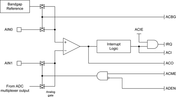
Figure 2-5. AVR analog comparator block diagram
When AIN0 is greater than AIN1, the comparator logic sets the comparator flag ACO. The output of the comparator can be configured to trigger the input capture function of one of the timer/counter modules, and it can also generate an interrupt specific to the comparator. The interrupt event can be configured to trigger on comparator output rise, fall, or toggle.
The analog comparator circuit can do more than just compare the voltages on the AIN0 and AIN1 inputs. The input of the analog comparator may also be configured such that the AIN1 input can be compared to the internal bandgap reference voltage, or AIN0 can be compared to the output of the ADC multiplexer (and this voltage is still available to the input of the ADC). The unusual symbols with four arrows are analog gates. How a gate will respond to a control input is indicated by the inversion circle—when the inverting control input is used it will pass an analog signal when the control is low, and otherwise it will pass a signal when it is high.
Analog-to-Digital Converter
Most AVR microcontrollers contain an 8-bit, 10-bit, or 12-bit analog-to-digital converter. The 8-bit converters are found in the ATtiny6 and ATtiny10 parts. Some of the automotive versions of AVR microcontrollers have no ADC.
When an ADC is part of the AVR design, it will have anywhere from 4 to 28 inputs. The actual number of available inputs depends largely on the physical package. Each input is selected one at a time via an internal multiplexer—they are not all active simultaneously. In addition, some of the I/O pins used by the ADC input multiplexer may also be assigned to other functions.
ATmega168 devices have either six or eight ADC input channels, depending on the package type. The PDIP (plastic DIP) package has a 10-bit ADC with six input channels. The TQFP and QFN/MFL surface-mount packages have a 10-bit ADC with eight input channels. Figure 2-6 shows a block diagram of the AVR ADC peripheral function.
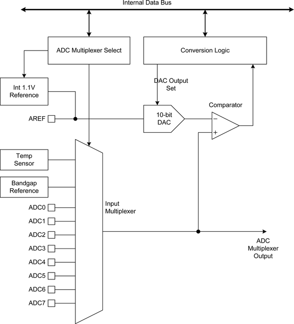
Figure 2-6. AVR analog-to-digital converter block diagram
Notice in Figure 2-6 that the AVR employs what is called a “successive approximation” converter. This type of converter isn’t particularly fast, but it is simple to implement, requiring only a DAC (digital-to-analog converter) and a comparator. The typical conversion time for a 10-bit AVR ADC in free-running mode, while still maintaining full resolution, is around 65 microseconds (µs) per sample.
Serial I/O
The ATmega168 provides three primary forms of serial interface: synchronous/asynchronous serial, SPI master/slave synchronous, and a byte-oriented two-wire interface similar to the Philips I2C (Inter-Integrated Circuit) standard.
USART
A common component of many AVR parts is a built-in USART (universal synchronous/asynchronous receiver-transmitter), also referred to as a UART (universal asynchronous receiver-transmitter). This function can be used to implement an RS-232 or RS-485 interface, or used without external interface logic for chip-to-chip communications. The baud rate is determined by the frequency of the clock used with the microcontroller, with 9,600 being a typical speed. Higher rates are possible with a fast external crystal. The USART can also be used in SPI (serial peripheral interface) mode, in addition to the dedicated SPI logic found in AVR devices. Figure 2-7 shows the basic internal components of the AVR USART peripheral function.
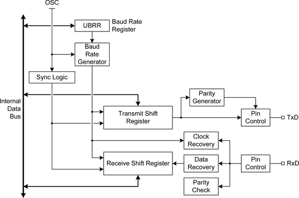
Figure 2-7. AVR USART block diagram
SPI
The SPI peripheral logic of the AVR supports all four standard SPI modes of operation. I/O pins on the AVR device may be configured to act as the MOSI, MISO, and SCK1 signals used by SPI. These pins are different from the RxD and TxD (recieve data and transmit data) pins used by the USART. Figure 2-8 shows a high-level view of the SPI logic.
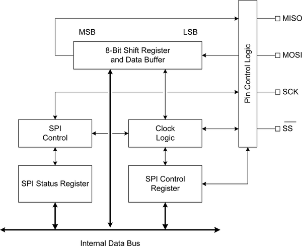
Figure 2-8. AVR SPI block diagram
TWI
The third form of serial I/O supported by many AVR devices is the two-wire interface (TWI). This interface is compatible with the Philips I2C protocol. It supports both master and slave modes of operation, and a 7-bit device address. The TWI interface can achieve transfer speeds of up to 400 kHz with multimaster bus arbitration and has the ability to generate a wakeup condition when the AVR is in sleep mode. Internally, the TWI peripheral is rather complex—much more so than either the USART or SPI peripherals. Figure 2-9 shows an overview of the TWI interface.
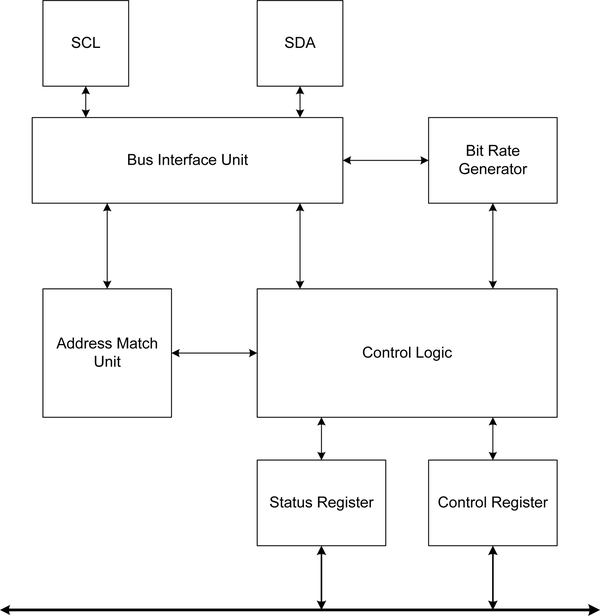
Figure 2-9. AVR TWI (I2C) block diagram
Interrupts
Interrupts are an essential function of a modern processor. They allow the processor to respond to events, either internal or external, by switching to a special block of interrupt handler code to deal with the interrupt. Once the block of code has been executed, control returns to the program that was interrupted at the place where the interrupt occurred. In the AVR an interrupt response may be enabled or disabled via bits in the control registers. This section is specific to the ATmega168. For other microcontroller types, refer to Appendix A or the official Atmel documentation.
The ATmega168 has two external interrupt inputs: INT0 and INT1. These inputs can be configured to trigger on a falling edge, a rising edge, or a low level. The EICRA control register (see Appendix B) is used to configure the behavior. INT0 and INT1 require the presence of an I/O clock. The low-level interrupt mode will generate interrupts as long as the input is held low.
The ATmega168 I/O pins can also serve as interrupt sources. The port-change interrupts are defined as PCINT0 through PCINT23, each of which is associated with one of the device’s I/O port pins. When enabled, an interrupt will be generated whenever the state of a port pin changes, even if the pin is configured to act as an output. This allows a pin to generate an interrupt under software control when a program toggles the state of the pin while the port change interrupt detect is enabled.
When any pin in the range from PCINT0 to PCINT7 changes, it will trigger the PCI0 interrupt. Pins in the range PCINT8 to PCINT14 will trigger PCI1, and pins in the range PCINT16 to PCTIN23 trigger the PCI2 interrupt. The registers PCMSK0, PCMSK1, and PCMSK2 control which pins contribute to pin change interrupts.
When an enabled interrupt occurs, the CPU will jump to a location in a vector table in memory that has been assigned to that particular interrupt. The address contains a jump instruction (RJMP) that points to the actual block of code for that interrupt. When the interrupt code is done, execution returns to the point in the original program where the interrupt occurred. Figure 2-10 shows how the interrupt vector table is used to switch execution to the interrupt code block, and then return control to the main program once the interrupt code is finished.
The ATmega168, for example, has a vector table with 26 entries, as shown in Table 2-1. For other processor types, refer to the Atmel documentation for more information on interrupts and how they are managed in the AVR devices.
| Vector | Address | Source | Definition |
|---|---|---|---|
1 |
0x0000 |
RESET |
External pin, power-on, brown-out, and watchd |
2 |
0x0002 |
INT0 |
External interrupt request 0 |
3 |
0x0004 |
INT1 |
External interrupt request 1 |
4 |
0x0006 |
PCINT0 |
Pin change interrupt request 0 |
5 |
0x0008 |
PCINT1 |
Pin change interrupt request 1 |
6 |
0x000A |
PCINT2 |
Pin change interrupt request 2 |
7 |
0x000C |
WDT |
Watchdog time-out interrupt |
8 |
0x000E |
TIMER2 |
COMPA Timer/Counter2 compare match A |
9 |
0x0010 |
TIMER2 |
COMPB Timer/Counter2 compare match B |
10 |
0x0012 |
TIMER2 |
OVF Timer/Counter2 overflow |
11 |
0x0014 |
TIMER1 |
CAPT Timer/Counter1 capture event |
12 |
0x0016 |
TIMER1 |
COMPA Timer/Counter1 compare match A |
13 |
0x0018 |
TIMER1 |
COMPB Timer/Counter1 compare match B |
14 |
0x001A |
TIMER1 |
OVF Timer/Counter1 overflow |
15 |
0x001C |
TIMER0 |
COMPA Timer/Counter0 compare match A |
16 |
0x001E |
TIMER0 |
COMPB Timer/Counter0 compare match B |
17 |
0x0020 |
TIMER0 |
OVF Timer/Counter0 overflow |
18 |
0x0022 |
SPI, STC |
SPI serial transfer complete |
19 |
0x0024 |
USART, RX |
USART, Rx complete |
20 |
0x0026 |
USART, UDRE |
USART, data register empty |
21 |
0x0028 |
USART, TX |
USART, Tx complete |
22 |
0x002A |
ADC |
ADC conversion complete |
23 |
0x002C |
EE READY |
EEPROM ready |
24 |
0x002E |
ANALOG COMP |
Analog comparator |
25 |
0x0030 |
TWI |
Two-wire serial interface |
26 |
0x0032 |
SPM READY |
Store program memory ready |
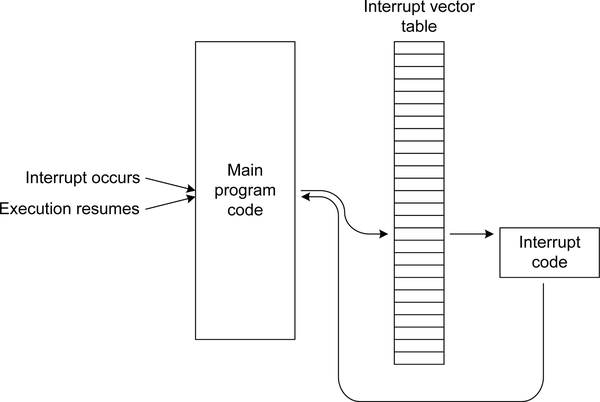
Figure 2-10. AVR interrupt vectors (ATmega168/328)
Watchdog Timer
The AVR provides a watchdog timer (WDT) with a configurable time-out period ranging from 16 ms to 8. If the WDT is enabled it can be used to generate a reset upon time-out, generate an interrupt on time-out, or a combination of both. It uses a separate on-chip oscillator, and because the WDT is clocked from a separate oscillator it will continue to count when the microcontroller is in sleep mode. It can therefore be used to awaken the microcontroller after a specific period of time.
Another common use for the WDT is to force either a reset or an interrupt if the timer expires without a reset action from the software. This is useful for forcing the microcontroller out of deadlocks or detecting runaway code.
Electrical Characteristics
The ATmega168 and ATmega328 AVR microcontrollers can operate with a VCC of 1.8 to 5.5V DC. The ATmega32U4 can utilize a VCC of 2.7 to 5.5V DC.
The current consumption of an AVR device will vary depending on the device type, the active or inactive (sleep) state of the microcontroller, and the clock speed. Values across the ATmega and XMEGA product lines range from 0.55 milliamps (mA) to 30 mA. The total current consumption is also dependent on the amount of current sourced through the I/O pins. Chapter 3 lists specific values for the ATmega168, ATmega328, ATmega1280, ATmega2560, and ATmega32U4 microcontrollers.
For More Information
Chapter 3 describes the pinouts used for the three types of AVR MCUs encountered on Arduino boards, and Chapter 4 shows how the AVR MCU pins are mapped to the I/O pins on various Arduino boards.
Each of the various AVR MCUs may have different combinations of internal peripheral functions, and in some cases the functionality may vary slightly between types. The best source of definitive information for AVR MCUs is the Atmel website.
1 Master out, slave in; master in, slave out; and serial clock.