
Appendix A
Generating Serial Presence Detection Data for Down Memory Configurations
I have no data yet. It is a capital mistake to theorize before one has data. Insensibly one begins to twist facts to suit theories, instead of theories to suit facts.
—Sherlock Holmes in “A Scandal in Bohemia”
This appendix provides guidance on how to create the SPD data required for motherboard designs that have the DDR3 SDRAM chips soldered directly onto the motherboard. Modular DIMMs normally have an SPD EERPOM that contains this information, which is used by the BIOS to correctly configure the system during Memory Reference Code. Without this data, the system will not boot; or at best it will try to boot with slow settings.
Since memory-down designs do not include DIMMs, they do not have ready-made SPD data on an EEPROM for the BIOS to read, and the board designer must assist BIOS or firmware developers to create the data. The data can then be put into an onboard EEPROM off the SMBus (as a physical DIMM would have), or the data can be hard-coded into the BIOS or placed into a table (or tables) where the BIOS can access the data during memory initialization. There are tradeoffs between these methods:
| Method | Pros | Cons |
| SPD EEPROM on | Single BIOS for any memory | 1. Cost of the EEPROM, |
| motherboard | configuration | 2. Need to program the SPD data during manufacturing |
| 3. Minor delay during initialization to fetch data across slower SMBus (several ms) | ||
| Hard-coding inline | 1. No EEPROM cost. | 1. BIOS has to change for every |
| in the memory code | 2. No programming of SPD on the | memory configuration |
| line | 2. Complexity during manufacturing | |
| 3. No added delay during initialization | ensuring correct BIOS per memory configuration | |
| Tables with optional | 1. No EEPROM | 1. Takes up hardware strap |
| hardware strap, | 2. No programming on line. | 2. BIOS will change when new |
| point memory init. | 3. No SMBus Read delays | configurations are designed |
| code to read from data file instead | 4. BIOS can read strap to know which memory configuration exists | |
| 5. Possible to upgrade with binary modification with a rebuild |
Hardcoding is not recommended for any solutions. Developers and designs should agree to include tables in the BIOS for various memory configuration (mimicking SPD data), or populate an actual SPD EEPROM on the board.
The following table shows the full list of the DDR3 SPD data that needs to be calculated for a memory-down solution. It assumes no SPD onboard. Each field can be calculated by analyzing the board’s topology and/or by using the datasheet for the SDRAM components used on the board. A “Typical Value” with its associated definition is also provided.


** Grayed out fields are different for Unbuffered and Registered DDR3 DRAM
Analyzing the Design’s Memory Architecture
The first step in creating the SPD data is to carefully analyze the design’s schematics to determine the overall memory architecture.
The used memory channels must be identified, and the number of “DIMM Equivalents” must be calculated by carefully noting which chip select pins on the DRAM controller are routed to the SDRAM chips.
Each “DIMM Equivalent” will require its own block of SPD data. The specific chip select pins, CS#[7:0] (the actual number of chip select pins can vary depending on the specific memory controller being used), have to be carefully analyzed to see which are being used by the SDRAM chips. It’s possible for designs to support single-rank, dual-rank, and quad-rank DIMM equivalents.
As an example, Figure A.1 shows an abstract view of DIMMs located on a single memory channel. Since each DIMM has only two CS# pins routed to the connector, this design supports two dual-rank DIMMs. If all four chip select pins were routed to a single DIMM, then the design would support a single, quad-rank DIMM.

Figure A.1: Chip Select Pins for a Single Memory Channel
Memory-down designs don’t use DIMMs; the SDRAM chips are soldered directly onto the motherboard. The chip select signals will be routed to the SDRAM chips in the same manner, however. In Figure A.2 below, on channel 0, only CS#[0] is connected to all eight SDRAM chips. Channel 0 is supporting only one single-rank DIMM equivalent. Channel 1 is also supporting a single- rank DIMM equivalent.
The data signals on the schematics must be analyzed to determine whether the down-on-board memory is implementing ECC or not. If the ECC data signals DDR_CB[7:0] (DDR “check bits,” although different chipsets might use different nomenclature) are being used as data signals on one of the SDRAM chips, then the memory subsystem on the board is implementing ECC Support. Some of the SPD fields must be set to indicate that the DIMM supports ECC.
The DRAM width can be determined by carefully analyzing the number of data signals, DDR_DQ[63:0], that are routed into each SDRAM chip. It will either be four, eight, sixteen, or thirty-two. This will indicate the DRAM width for the DRAM chip in this DIMM equivalent.
The DRAM width is part of SPD field 7, and often there are slight timing differences in the datasheet depending on the width of the specific DRAM being used.
The vendor and exact part number of the SDRAM chips used in the design is extracted from the schematics. The full datasheet must be obtained in order to calculate all of the needed SPD fields.
SDRAM Architecture Analysis Example
Figure A.2 shows a typical memory-down implementation. Sixteen SDRAM chips are split evenly across two of three available channels. All the SDRAM chips on a given channel are connected to a single chip select signal. Since each SDRAM chip is connected to eight data signals, this design consists of two single-rank DIMM equivalents using ×8 width MT41J256M8HX-187-EITF SDRAM devices. Since the ECC data lines are not being used (not shown, but they would have required the use of an additional ×8 SDRAM chip per channel), both DIMM equivalents are non-ECC.
Analyzing the schematics provides the SDRAM width and rank information (SPD field #7). All the other information required in the SPD data block will have to be extracted from the MT41J256M8HX-187-EITF datasheet. This process is described in the next section.
Calculating Specific SPD Data Based on SDRAM Datasheet
This section will go through each SPD field and explain how to extract the data for the field out of the SDRAM datasheet. This section will use the SDRAM configuration shown in Figure A.2, using the MT41J256M8HX-187-EITF datasheet. Note that each section number will correspond to the SPD field offset.
Each field will contain:
–The exact definition out of the JEDEC DDR3 specification.
–The appropriate section out of the MT41J256M8HX-187-EITF datasheet

Figure A.2: Schematic Analysis Example
See the “References” section at the end of this appendix for links to the exact documents used.
SPD Field 0x00: Number of Bytes
SPD EEPROMs typically contain 256 bytes. Down-on-board memory designs should use 0x11 for this field.

Byte 0: Number of Bytes Used ⁄ Number of Bytes in SPD Device ⁄ CRC Coverage
The least significant nibble of this byte describes the total number of bytes used by the module manufacturer for the SPD data and any (optional) specific supplier information. The byte count includes the fields for all required and optional data. Bits 6–4 describe the total size of the serial memory used to hold the Serial Presence Detect data. Bit 7 indicates whether the unique module identifier (found in bytes 117–125) is covered by the CRC encoded on bytes 126 and 127.
| Bit 7 | Bits 6:4 | Bits 3:0 |
| CRC Coverage | SPD Bytes Total | SPD Bytes Used |
| 0 = CRC covers bytes 0–125 | Bit [6, 5, 4]: | Bit [3, 2, 1, 0]: |
| 1 = CRC covers bytes 0–116 | 000 = Undefined | 0000 = Undefined |
| 001 = 256 | 0001 = 128 | |
| All others reserved | 0010 = 176 | |
| 0011 = 256 | ||
| All others reserved |
Down-on-board memory designs should use 0×10 for this field.

This byte describes the compatibility level of the encoding of the bytes contained in the SPD EEPROM, and the current collection of valid defined bytes. Software should examine the upper nibble (Encoding Level) to determine if it can correctly interpret the contents of the module SPD. The lower nibble (Additions Level) can optionally be used to determine which additional bytes or attribute bits have been defined; however, since any undefined additional byte must be encoded as 0×00 or undefined attribute bit must be defined as 0, software can safely detect additional bytes and use safe defaults if a zero encoding is read for these bytes.


The Additions Level is never reduced even after an increment of the Encoding Level. For example, if the current SPD revision level were 1.2 and a change in Encoding Level were approved, the next revision level would be 2.2. If additions to revision 2.2 were approved, the next revision would be 2.3. Changes in the Encoding Level are extremely rare, however, since they can create incompatibilities with older systems.
The exceptions to the above rule are the SPD revision levels used during development prior to the Revision 1.0 release. Revisions 0.0 through 0.9 are used to indicate sequential pre-production SPD revision levels; however, the first production release will be Revision 1.0.
DDR3 DIMMs are programmed with the value 0×0B.

Per JEDEC Specification, Byte 2: Key Byte ⁄ DRAM Device Type
This byte is the key byte used by the system BIOS to determine how to interpret all other bytes in the SPD EEPROM. The BIOS must check this byte first to ensure that the EEPROM data is interpreted correctly. Any DRAM or module type that requires significant changes to the SPD format (beyond defining previously undefined bytes or bits) also requires a new entry in the key byte table below.

This field is typically set to 0×02 for Unbuffered DIMMs or 0×03 when using SO-DIMMs. If the specific chipset/CPU ONLY supports SO-DIMMs, use 0×03 so as not to confuse the BIOS.

Per JEDEC Specification, Byte 3: Key Byte ⁄ Module Type
This byte is a Key Byte used to index the module specific section of the SPD from bytes 60–116. Byte 3 identifies the SDRAM memory module type, which implies the width (D dimension) of the module. Other module physical characteristics, such as height (A dimension) or thickness (E dimension) are documented in the module-specific section of the SPD. Refer to the relevant JEDEC JC-11 module outline (MO) documents for dimension definitions.
SPD Field 0×04: SDRAM Density and Banks

Byte 4: SDRAM Density and Banks
This byte defines the total density of the DDR3 SDRAM, in bits, and the number of internal banks into which the memory array is divided. These values come from the DDR3 SDRAM datasheet.
| Bit 7 | Bits 6:4 | Bits 3:0 |
| Reserved | Bank Address Bits | Total SDRAM Capacity in Megabits (Mb) |
| 000 = 3 (8 banks) | 0000 = 256 Mb | |
| 001 = 4 (16 banks) | 0001 = 512 Mb | |
| 010 = 5 (32 banks) | 0010 = 1 Gb | |
| 011 = 6 (64 banks) | 0011 = 2 Gb | |
| All others reserved | 0100 = 4 Gb | |
| 0101 = 8 Gb | ||
| 0110 = 16 Gb | ||
| All others reserved |

SPD Field #4: “SDRAM Density and Banks” Example from Micron T41J256M8 Datasheet
This field is typically extracted directly from the SDRAM datasheet. Often the bank bits are specified instead of the number of banks (that is, three bank bits would provide eight banks, total). Likewise, in the odd situation where the DRAM density (or capacity) is not obviously spelled out in the datasheet, it can be calculated by multiplying the full address range by the DRAM width:
Density (Capacity) = 2 (Rows + Columns + Bank Bits) × DRAM Width
SPD Field 0×05: SDRAM Rows and Columns

From JEDEC Specification, Byte 5: SDRAM Addressing
This byte describes the row addressing and the column addressing in the SDRAM device. Bits 2–0 encode the number of column address bits, and bits 5–3 encode the number of row address bits. These values come from the DDR3 SDRAM datasheet.
| Bit 7:6 | Bits 5:3 | Bits 2:0 |
| Reserved | Row Address Bits | Column Address Bits |
| 000 = 12 | 000 = 9 | |
| 001 = 13 | 001 = 10 | |
| 010 = 14 | 010 = 11 | |
| 011 = 15 | 011 = 12 | |
| 100 = 16 | All others reserved | |
| All others reserved |
Table 2 Addressing

SPD Field #5: “SDRAM Rows & Columns” Example from Micron MT41J256M8 Datasheet
Rows and columns are the number of address signals that are active when the RAS# and CAS# signals strobe respectively. The row and column values required by the SPD data are extracted directly from the SDRAM datasheet as shown above. Here, A[9:0] consists of ten individual address lines, not nine. Both column and row fields required in the SPD data are not nibble aligned. This is a common mistake with this field.
SPD Field 0×06: Nominal Voltage, VDD
Below is an example of a 1.5V part; this will be modified per the components used in the design.

Byte 6: Module Nominal Voltage, VDD
This byte describes the Voltage Level for DRAM and other components on the module such as the register if applicable. Note that SPDs or thermal sensor components are on the VDDSPD supply and are not affected by this byte. “Operable” is defined as the VDD voltage at which module operation is allowed using the performance values programmed in the SPD. “Endurant” is defined as the VDD voltage at which the module may be powered without adversely affecting the life expectancy or reliability. Further specifications will exist to define the amount of time that the “Endurant” voltage can be applied to the module. Operation is not supported at this voltage.

The nominal Voltage parameter is extracted directly from the SDRAM datasheet, usually on the front page.
SPD Field 0×07: Ranks & Device DQ Count

From the JEDEC Specification, Byte 7: Module Organization
This byte describes the organization of the SDRAM module. Bits 2–0 encode the device width of the SDRAM devices. Bits 5–3 encode the number of physical ranks on the module. For example, for a double-rank module with ×8 DRAMs, this byte is encoded 00 001 001, or 0×09.
| Bit 7:6 | Bits 5:3 | Bits 2:0 |
| Reserved | Number of Ranks | SDRAM Device Width |
| 0 00 = 1 Rank | 000 = 4 bits | |
| 001 = 2 Ranks | 001 = 8 bits | |
| 010 = 3 Ranks | 010 = 16 bits | |
| 011 = 4 Ranks | 011 = 32 bits | |
| All others reserved | All others reserved |

SPD Field #7: “Ranks & Device DQ Count” Example from Micron MT41J256M8 Datasheet
The SDRAM device width also can be easily discerned by looking at the schematics and noting the number of data lines used by each SDRAM device. SDRAM devices use four, eight, sixteen, or thirty-two data signals. The Number of Ranks is trickier to calculate. This parameter is not associated with the SDRAM chips, but is a parameter relating to the DIMM itself. It is the number or rank signals or chip selects used in the DIMM equivalent. The proper value to use must be extracted from the schematics. Note the specific chip select pins being used on a given channel. If only CS0 is routed to the SDRAM chips, then the down-on-board memory solution is single rank (1 rank). If both CS0 and CS1 are routed to all of the SDRAM chips, the down-on-board memory solution is dual rank (two ranks). Some server chipsets also support quad-rank DIMMs.
In extreme cases, it might be necessary to analyze the chipset’s datasheet and design guide to discern exactly which DIMM equivalent(s) are being used in the down-on-board memory design.
As an example, let’s assume that an Intel® 5100 chipset based design has SDRAM chips connected using all four rank signals (CS[3:0]#). This implementation could either be a single quad-rank DIMM equivalent, or two dual-rank DIMM equivalent. As shown in the two figures below, taken from this document: Intel® Xeon® Processor 5000 Sequence with Intel® 5100 Memory Controller Hub Chipset for Communications, Embedded, and Storage Applications Platform Design Guide (PDG) April 2009 Revision 2.3 Document Number: 352108–2.3.
All other memory interface signals have to be analyzed. For example, if the design is routing a SINGLE clock to all of the SDRAM chips (DCLKP/N [0]), then the implementation is similar to that in Figure 37; it’s a single quad-rank DIMM implementation. However, if half of the SDRAM chips are connected to DCLKP/N[0], and the other half are connected to DCLKP/N[1], then the design is implementing two DIMM equivalents of dual-rank DIMMs.

Figure 37 Configuration 1.1 - Clock and Control Signal DIMM Pin Mapping (One DIMM per Channel - 32 GB Mode, Quad-rank with S3 Support)
Figure 37 from Intel® 5100 Platform Design Guide–Single QuAD- Rank DIMM equi1valent

Figure 38 Configuration 2.1 - Clock and Control Signal DIMM Pin Mapping
(Two DIMMs Per Channel - 32 GB Mode)
Figure 38 from Intel® 5100 Platform Design Guide–Single QuAD-Rank DIMM equivalent
SPD Field 0×08: Module Bus Width
This field is set t0 0×0Bh (72 bits) if the design is implementing ECC. Otherwise, set this field to 0×03h.

Byte 8: Module Memory Bus Width
This byte describes the width of the SDRAM memory bus on the module. Bits 2–0 encode the primary bus width. Bits 4–3 encode the bus extensions such as parity or ECC.
Examples:
–64-bit primary bus, no parity or ECC (64 bits total width): xxx 000 011
–64-bit primary bus, with 8 bit ECC (72 bits total width): xxx 001 011
SPD Field 0×09: Fine Timebase Dividend/Divisor
Setting this value to 0×52 (2.5ps) works well for implementing the other timing fields based on this value. Most DDR3 DIMMs use 0×52 for this field.

Per JEDEC Specification, Byte 9: Fine Timebase (FTB) Dividend ⁄ Divisor
This byte defines a value in picoseconds that represents the fundamental timebase for fine grain timing calculations. This value is used as a multiplier for formulating subsequent timing parameters. The fine timebase (FTB) is defined as the fine timebase dividend, bits 7–4, divided by the fine timebase divisor, bits 3–0.
| Bits 7:4 | Bits 2:0 |
| Fine Timebase (FTB) Dividend | Fine Timebase (FTB) Divisor |
| Values defined from 1 to 15 | Values defined from 1 to 15 |
Examples:

SPD Field 0×0A and 0×0B: Medium Timebase Dividend/Divisor
Most DDR3 DIMM’s SPD data use 0×01h (0.125 ns) for this value.

Byte 10: Medium Timebase (MTB) Dividend
Byte 11: Medium Timebase (MTB) Divisor
These bytes define a value in nanoseconds that represents the fundamental timebase for medium grain timing calculations. This value is typically the greatest common divisor for the range of clock frequencies (clock periods) supported by a particular SDRAM. This value is used as a multiplier for formulating subsequent timing parameters. The Medium Timebase (MTB) is defined as the Medium Timebase Dividend (byte 10) divided by the medium timebase divisor (byte 11).
| Byte 10, Bits 7:0 | Byte 11, Bits 7:0 |
| Medium Timebase (MTB) Dividend | Medium Timebase (MTB) Divisor |
| Values defined from 1 to 255 | Values defined from 1 to 255 |

To simplify BIOS implementation, DIMMs associated with a given key byte value may differ in MTB value only by a factor of two. For DDR3 modules, the defined MTB values are:

SPD Field 0x0C: Cycle Time (tCKmin)
This field can be tricky to calculate.
- Find the lowest tCK number in the SDRAM datasheet for CAS Latencies supported by that SDRAM chip (see SPD field 14 below). The example above from the Micron MT41J256M8 gives 1.875 ns.
- This number must be divided by the Medium Timebase Divisor, the value in 0×0B. In our example this is 0.125 ns.
- 3. 1.875 ns ⁄ 0.125 ns = 15 = 0×0F.

Per JEDEC Specification, Byte 12: SDRAM Minimum Cycle Time (tCKmin)
This byte defines the minimum cycle time for the SDRAM module, in Medium Timebase (MTB) units. This number applies to all applicable components on the module. This byte applies to SDRAM and support components as well as the overall capability of the DIMM. This value comes from the DDR3 SDRAM and support component datasheets.
| Bits 7:0 |
| Minimum SDRAM Cycle Time (tCKmin) MTB Units |
| Values defined from 1 to 255 |
If tCKmin cannot be divided evenly by the MTB, this byte must be rounded up to the next larger integer and the Fine Offset for tCKmin (SPD byte 34) used for correction to get the actual value.

Notes: 1. See SPD byte 34
Table 53 DDR3-1066 Speed Bins


Notes:
- tREFI depends on TOPER.
- The CL and CWL settings result in tCK requirements. When selecting tCK, both CL and CWL requirement settings need to be fulfilled.
- Reserved settings are not allowed.
SPD Field #12: “Cycle Time (tCKmin)” Example from Micron MT41J256M8 Datasheet
SPD Field 0×0E and 0×0F: CAS Latencies Supported
The supported CAS latencies can be found in the SDRAM datasheet as shown above. Each supported CAS latency must have its bit set in fields 14 and 15.

From the JEDEC Specification:
Byte 14: CAS Latencies Supported, Least Significant Byte
Byte 15: CAS Latencies Supported, Most Significant Byte
These bytes define which CAS Latency (CL) values are supported. The range is from CL = 4 through CL = 18 with one bit per possible CAS Latency. A 1 in a bit position means that CL is supported, a 0 in that bit position means it is not supported. Since CL = 6 is required for all DDR3 speed bins, bit 2 of SPD byte 14 is always 1. These values come from the DDR3 SDRAM datasheet.

0 means this CAS Latency is not supported
1 means this CAS Latency is supported.
SPD Field #14 and #15: “CAS Latencies Supported” Definition from JEDEC DDR3 SPD Specification
Table 53 DDR3-1066 Speed Bins

Notes:
1. tREFI depends on TOPER.
2. The CL and CWL settings result in tCK requirements. When selecting tCK, both CL and CWL requirement settings need to be fulfilled.
3. Reserved settings are not allowed.
SPD Field #14 and #15: “CAS Latencies Supported” Example from Micron MT41J256M8 Datasheet
SPD Field 0×10: CAS Latency Time (tAAmin or tCL)
This field must also be extracted from the datasheet and divided by the Medium Timebase Divisor. Although the SPD specification calls out this abbreviation as tAA, I’ve found that it is usually abbreviated tCL or just “CL” in the various SDRAM datasheets (as shown above).
In our example:
1.The tCL value found in the Micron MT41J256M8 datasheet for our specific SDRAM chip gives 13.1 ns.
2.This number must be divided by the Medium Timebase Divisor, the value in 0×0B. In our example this is 0.125 ns.
3.13.1 ns ⁄ 0.125 ns = 104.8 (round up) = 0×69.

Byte 16: Minimum CAS Latency Time (tAAmin)
This byte defines the minimum CAS Latency in Medium Timebase (MTB) units. Soft-
ware can use this information, along with the CAS Latencies supported (found in bytes 14 and 15) to determine the optimal cycle time for a particular module. This value comes from the DDR3 SDRAM datasheet.
| Bits 7:0 |
| Minimum SDRAM CAS Latency Time (tAAmin) MTB Units Values defined from 1 to 255 |
If tAAmin cannot be divided evenly by the MTB, this byte must be rounded up to the next larger integer and the Fine Offset for tAAmin (SPD byte 35) used for correction to get the actual value.
Examples:


Notes:
- See SPD byte 35.
- Refer to device datasheet for downbin support details.
SPD Field #16: “Minimum CAS Latency Time (tAAmin)” Definition from JEDEC DDR3 SPD Specification
Table 1 Key Timing Parameters

1.Backward compatible to 1066, CL = 7 (-187E).
2.Backward compatible to 1333, CL = 9 (-15E).
3.Backward compatible to 1066, CL = 8 (-187).
SPD Field #16: “Minimum CAS Latency Time (tAAmin)” Example from Micron MT41J256M8 Datasheet
SPD Field 0×11: Write Recovery Time (twrmin)
This is another field that must be extracted from the datasheet and divided by the Medium Timebase Divisor.
In our example:
1.The tWR value found in the Micron MT41J256M8 datasheet for our specific SDRAM chip gives 15 ns.
2.This number must be divided by the Medium Timebase Divisor, the value in 0×0B. In our example this is 0.125 ns.
3.15 ns /0.125 ns = 120 = 0×78.

From the JEDEC Specification: Byte 17: Minimum Write Recovery Time (tWRmin)
This byte defines the minimum SDRAM write recovery time in Medium Timebase (MTB) units. This value comes from the DDR3 SDRAM datasheet.
| Bits 7–0 |
| Minimum Write Recovery Time (tWR) MTB Units |
| Values defined from 1 to 255 |
Example:

Steps:
1.The BIOS first determines the common operating frequency of all modules in the system, ensuring that the corresponding value of tCK (tCKactual) falls between tCKmin (Bytes 12 and 34) and tCKmax. If tCKactual is not a JEDEC standard value, the next smaller standard tCKmin value is used for calculating Write Recovery.
2.The BIOS then calculates the “desired” Write Recovery (WRdesired):
WRdesired = ceiling ( tWRmin ⁄ tCKactual )
where tWRmin is defined in Byte 17. The ceiling function requires that the quotient be rounded up always.
3.The BIOS then determines the “actual” Write Recovery (WRactual):
WRactual = max (WRdesired, min WR supported)
where min WR is the lowest Write Recovery supported by the DDR3 SDRAM. Note that not all WR values supported by DDR3 SDRAMs are sequential, so the next higher supported WR value must be used in some cases. Usage example for DDR3-1333G operating at DDR3-1333:
tCKactual = 1.5 ns
WRdesired = 15 /1.5 = 10
WRactual = max(10, 10) = 10
Table 56 Electrical Characteristics and AC Operating Conditions (Continued) Notes 1–8 apply to the entire table


SPD Field #17: “Minimum Write Recovery Time (tWRmin)” Example from Micron MT41J256M8 Datasheet
SPD Field 0×12 RAS# to CAS# Delay (tRCDmin)
This field must also be extracted from the datasheet and divided by the Medium Timebase Divisor.
In our example:
1.The tRCD value found in the Micron MT41J256M8 datasheet for our specific SDRAM chip gives 13.1 ns.
2.This number must be divided by the Medium Timebase Divisor, the value in 0×0B. In our example this is 0.125 ns.
3.13.1 ns ⁄ 0.12 5ns = 104.8 (round up) = 0×69.

Byte 18: Minimum RAS# to CAS# Delay Time (tRCDmin)
This byte defines the minimum SDRAM RAS# to CAS# Delay in Medium Timebase (MTB) units. This value comes from the DDR3 SDRAM datasheet.
| Bits 7–0 |
| Minimum RAS# to CAS# Delay (tRCD) MTB Units |
| Values defined from 1 to 255 |
If tRCDmin cannot be divided evenly by the MTB, this byte must be rounded up to the next larger integer and the Fine Offset for tRCDmin (SPD byte 36) used for correction to get the actual value.
Examples:


Notes:
1.1. See SPD byte 36.
2.Refer to device datasheet for downbin support details.
SPD Field #18: “Minimum RAS# to CAS# Delay Time (tRCDmin)” Definition from JEDEC DDR3 SPD Specification
Table 1 Key Timing Parameters

Notes:
- Backward compatible to 1066, CL = 7 (-187E).
- Backward compatible to 1333, CL = 9 (-15E).
- Backward compatible to 1066, CL = 8 (-187).
SPD Field #18: “Minimum RAS# to CAS# Delay Time (tRCDmin)”
Example from Micron MT41J256M8 Datasheet
SPD Field 0x13: Min. Row Active to Row Active Delay (tRRDmin)
This field must also be extracted from the datasheet and divided by the Medium Timebase Divisor. In our example:
1. The tRRD value found in the Micron MT41J256M8 datasheet for our specific SDRAM chip gives 7.5 ns.
2.This number must be divided by the Medium Timebase Divisor, the value in 0×0B. In our example this is 0.125 ns.
3.7.5 ns ⁄ 0.125 ns = 60 = 0×3C.

Byte 19: Minimum Row Active to Row Active Delay Time (tRRDmin)
This byte defines the minimum SDRAM Row Active to Row Active Delay Time in Medium Timebase units. This value comes from the DDR3 SDRAM datasheet. The value of this number may be dependent on the SDRAM page size; please refer to the DDR3 SDRAM datasheet section on Addressing to determine the page size for these devices. Controller designers must also note that at some frequencies, a minimum number of clocks may be required, resulting in a larger tRRDmin value than indicated in the SPD. For example, tRRDmin for DDR3-800 must be 4 clocks.
| Bits 7–0 |
| Min. Row Active to Row Active Delay (tRRDmin) |
| Values defined from 1 to 255 |

Note: tRRD is at least 4 nCK independent of operating frequency.
Table 56 Electrical Characteristics and AC Operating Conditions (Continued) Notes 1–8 apply to the entire table


SPD Field #19: “Minimum Row Active to Row Active Delay Time (tRRDmin)” Example from Micron MT41J256M8 Datasheet
SPD Field 0×14: Min. Row Precharge Delay (tRPmin)
This is another field that must be extracted from the datasheet and divided by the Medium Timebase Divisor.
In our example:
1.The tRP value found in the Micron MT41J256M8 datasheet for our specific SDRAM chip gives 13.125 ns.
2.This number must be divided by the Medium Timebase Divisor, the value in 0×0B. In our example this is 0.125 ns.
3.13.125 ns ⁄ 0.125 ns = 105 = 0×69.

Byte 20: Minimum Row Precharge Delay Time (tRPmin)
This byte defines the minimum SDRAM Row Precharge Delay Time in Medium Timebase (MTB) units. This value comes from the DDR3 SDRAM datasheet.
| Bits 7–0 |
| Min. Row Active to Row Active Delay (tRRDmin) |
| Values defined from 1 to 255 |
If tRPmin cannot be divided evenly by the MTB, this byte must be rounded up to the next larger integer and the Fine Offset for tRPmin (SPD byte 37) used for correction to get the actual value.


Notes:
1. See SPD byte 37.
2. Refer to device datasheet for downbin support details.
Table 53 DDR3-1066 Speed Bins


Notes:
1. tREFI depends on TOPER.
2. The CL and CWL settings result in tCK requirements. When selecting tCK, both CL and CWL requirement settings need to be fulfilled.
3. Reserved settings are not allowed.
SPD Field #20: “Minimum Row Precharge Delay Time (tRPmin)” Micron MT41J256M8 Datasheet
SPD Field 0×15: Upper Nibble of tRAS & tRC
This field is the Most Significant nibble (4 bits) for both the Active to Precharge Delay (tRASmin) and Active to Active/Refresh delay (tRCmin). See the next two sections for how to determine the tRASmin and tRCmin values and put the upper nibble of those results into this field.

Byte 21: Upper Nibbles for tRAS and tRC
This byte defines the most significant nibbles for the values of tRAS (byte 22) and tRC (byte 23). These values come from the DDR3 SDRAM datasheet.
| Bits 7–4 | Bits 3–0 |
| tRC Most Significant Nibble | tRAS Most Significant Nibble |
| See Byte 23 description | See Byte 22 description |
SPD Field #21: “Upper Nibbles for tRAS and tRC” Definition from JEDEC DDR3 SPD Specification
SPD Field 0×16: Min. Active to Precharge Delay (tRASmin) LSB
This is another field that must be extracted from the datasheet and divided by the Medium Timebase Divisor. In our example:
1.The tRAS value found in the Micron MT41J256M8-187E datasheet for our specific SDRAM chip gives 37.5 ns.
2.This number must be divided by the Medium Timebase Divisor, the value in 0×0B. In our example this is 0.125 ns.
3.37.5 ns /0.125 ns = 300 = 0×012C.
4.The LSB, 0×2C, goes into SPD field #22 (0×16).
5.The lower nibble of the MSB, 0×01, goes into bits [3:0] of SPD field #21 (0×15)

Byte 22: Minimum Active to Precharge Delay Time (tRASmin), Least Significant Byte
The lower nibble of Byte 21 and the contents of Byte 22 combined create a 12-bit value that defines the minimum SDRAM Active to Precharge Delay Time in Medium Timebase (MTB) units. The most significant bit is Bit 3 of Byte 21, and the least significant bit is Bit 0 of Byte 22. This value comes from the DDR3 SDRAM datasheet.
| Byte 21 Bits 3–0, Byte 22 Bits 7–0 |
| Minimum Active to Precharge Time (tRAS) MTB Units |
| Values defined from 1 to 4095 |
Examples:


SPD Field #22: “Minimum Active to Precharge Delay Time (tRASmin)” Definition from JEDEC DDR3 SPD Specification
Table 53 DDR3-1066 Speed Bins


Notes:
1. tREFI depends on TOPER.
2. The CL and CWL settings result in tCK requirements. When selecting tCK, both CL and CWL requirement settings need to be fulfilled.
3. Reserved settings are not allowed.
SPD Field #22: “Minimum Active to Precharge Delay Time (tRASmin)” Example from Micron MT41J256M8 Datasheet
SPD Field 0×17: Min. Active to Active Refresh Delay (tRCmin) LSB
This is another field that must be extracted from the datasheet and divided by the Medium Timebase Divisor. In our example:
1.The tRC value found in the Micron MT41J256M8-187E datasheet for our specific SDRAM chip gives 50.625 ns.
2.This number must be divided by the Medium Timebase Divisor, the value in 0×0B. In our example this is 0.125 ns.
3.50.625 ns ⁄ 0.125 ns = 405 = 0×0195.
4.The LSB, 0×95, goes into SPD field #23 (0×17).
5.The lower nibble of the MSB, 0x01, goes into bits [7:4] of SPD field #21 (0×15).

Byte 23: Minimum Active to Active/Refresh Delay Time (tRCmin), Least Significant Byte
The upper nibble of Byte 21 and the contents of Byte 23 combined create a 12-bit value that defines the minimum SDRAM Active to Active/Refresh Delay Time in Medium Timebase (MTB) units. The most significant bit is Bit 7 of Byte 21, and the least significant bit is Bit 0 of Byte 23. This value comes from the DDR3 SDRAM datasheet.

1.See SPD byte 38.
2.Refer to device datasheet for downbin support details.
SPD Field #23: “Minimum Active to Active/Refresh Delay Time (tRCmin)” Definition from JEDEC DDR3 SPD Specification
Table 53 DDR3-1066 Speed Bins

Notes:
1. tREFI depends on TOPER.
2. The CL and CWL settings result in tCK requirements. When selecting tCK, both CL and CWL requirement settings need to be fulfilled.
3. Reserved settings are not allowed.
SPD Field #23: “Minimum Active to Active/Refresh Delay Time (tRCmin)” Example from Micron MT41J256M8 Datasheet
SPD Field 0×18 and 0×19: Min. Refresh Recovery Delay (tRFCmin)
This is another field that must be extracted from the datasheet and divided by the Medium Timebase Divisor. In our example:
1.The tRFC value found in the Micron MT41J256M8-187E datasheet for our specific SDRAM chip gives 160 ns. Note that the MT41J256M8-187E is a 2 Gb part.
2.This number must be divided by the Medium Timebase Divisor, the value in 0×0B. In our example this is 0.125 ns.
3.50.625 ns ⁄ 0.125 ns = 1280 = 0×0500.
4.The LSB, 0×00, goes into SPD field #24 (0×18).
5.The MSB, 05, goes into SPD field #25 (0×19).

Byte 24: Minimum Refresh Recovery Delay Time (tRFCmin), Least Significant Byte
Byte 25: Minimum Refresh Recovery Delay Time (tRFCmin), Most Significant Byte
The contents of Byte 24 and the contents of Byte 25 combined create a 16-bit value that defines the minimum SDRAM Refresh Recovery Time Delay in Medium Timebase (MTB) units. The most significant bit is Bit 7 of Byte 25, and the least significant bit is Bit 0 of Byte 24. These values come from the DDR3 SDRAM datasheet.
| Byte 25 Bits 7–0, Byte 24 Bits 7–0 |
| Minimum Refresh Recover Time Delay (tRFC) MTB Units |
| Values defined from 1 to 65535 |
Examples:

SPD Field #24 and #25: “Minimum Refresh Recovery Delay Time (tRFCmin), LSB” Definition from JEDEC DDR3 SPD Specification
Table 56 Electrical Characteristics and AC Operating Conditions (Continued) Notes 1–8 apply to the entire table

SPD Field #24 and #25: “Minimum Refresh Recovery Delay Time (tRFCmin), LSB”
Micron MT41J256M8 Datasheet
SPD Field 0×1A: Min. Write to Read Command Delay (tWTRmin)
This is another field that must be extracted from the datasheet and divided by the Medium Timebase Divisor. In our example:
1.The tWTR value found in the Micron MT41J256M8 datasheet for our specific SDRAM chip gives 7.5 ns.
2.This number must be divided by the Medium Timebase Divisor, the value in 0×0B. In our example this is 0.125 ns.
3.75 ns /0.125 ns = 60 = 0×3C.

Byte 26: Minimum Internal Write to Read Command Delay Time (tWTRmin)
This byte defines the minimum SDRAM Internal Write to Read Delay Time in Medium Timebase (MTB) units. This value comes from the DDR3 SDRAM datasheet. The value of this number may be dependent on the SDRAM page size; please refer to the DDR3 SDRAM datasheet section on Addressing to determine the page size for these devices. Controller designers must also note that at some frequencies, a minimum number of clocks may be required, resulting in a larger tWTRmin value than indicated in the SPD. For example, tWTRmin for DDR3-800 must be 4 clocks.
| Bits 7–0 |
| Internal Write to Read Delay Time (tWTR) MTB Units |
| Values defined from 1 to 255 |
Example:

Note: tRTP is at least 4 nCK independent of operating frequency.
SPD Field #26: “Minimum Internal Write to Read Command Delay Time (tWTRmin)” Definition from JEDEC DDR3 SPD Specification
Table 56 Electrical Characteristics and AC Operating Conditions (Continued) Notes 1–8 apply to the entire table


SPD Field #26: “Minimum Internal Write to Read Command Delay Time (tWTRmin)” Example from Micron MT41J256M8 Datasheet
SPD Field 0×1B: Min. Read to Precharge Command Delay (tRTPmin)
This is another field that must be extracted from the datasheet and divided by the Medium Timebase Divisor.
In our example:
1.The tRTP value found in the Micron MT41J256M8 datasheet for our specific SDRAM chip gives 7.5 ns.
2.This number must be divided by the Medium Timebase Divisor, the value in 0×0B. In our example this is 0.125 ns.
3.75 ns ⁄ 0.125 ns = 60 = 0×3C.

Byte 27: Minimum Internal Read to Precharge Command Delay Time (tRTPmin)
This byte defines the minimum SDRAM Internal Read to Precharge Delay Time in Medium Timebase (MTB) units. This value comes from the DDR3 SDRAM datasheet. The value of this number may depend on the SDRAM page size; please refer to the DDR3 SDRAM datasheet section on Addressing to determine the page size for these devices. Controller designers must also note that at some frequencies, a minimum number of clocks may be required, resulting in a larger tRTPmin value than indicated in the SPD. For example, tRTPmin for DDR3-800 must be 4 clocks.
| Bits 7–0 |
| Internal Read to Precharge Delay Time (tRTP) MTB Units |
| Values defined from 1 to 255 |
Examples:

Note: tRTP is at least 4 nCK independent of operating frequency.
SPD Field #27: “Minimum Internal Read to Precharge Command Delay Time (tRTPmin)” Definition from JEDEC DDR3 SPD Specification
Table 56 Electrical Characteristics and AC Operating Conditions (Continued) Notes 1–8 apply to the entire table


SPD Field #27: “Minimum Internal Read to Precharge Command Delay Time (tRTPmin)” Example from Micron MT41J256M8 Datasheet
SPD Field 0×1C: tFAW Upper Nibble
This is the upper nibble for the tFAW SDRAM timing parameter. See the next section for how to calculate this value, and put the upper nibble into SPD Field #28, bits [3:0].

Byte 28: Upper Nibble for tFAW
This byte defines the most significant nibble for the value of tFAW (SPD byte 29). This value comes from the DDR3 SDRAM datasheet.
| Bits 7–4 | Bits 3–0 |
| Reserved | tfaw Most Significant Nibble |
| Reserved | See Byte 29 description |
SPD Field #28: “Upper Nibble for tFAW” Definition from JEDEC DDR3 SPD Specification
SPD Field 0×1D: Min. Four Activate Window Delay (tFAWmin) LSB
This is another field that must be extracted from the datasheet and divided by the Medium Timebase Divisor. In our example:
1.The tFAW value found in the Micron MT41J256M8 datasheet for our specific SDRAM chip gives 37.5 ns. Note that in the case of this SDRAM part, the number varies, depending on the part’s page size. In the case of the MT41J256M8, the page size is 1K as shown.
2.This number must be divided by the Medium Timebase Divisor, the value in 0×0B. In our example this is 0.125 ns.
3.37.5 ns /0.125 ns = 300 = 0×12C.
4.The upper nibble, 0×1, is put into SPD field #28, bits [3:0].
5.The LSB, 0×2C, is put into SPD field #29.

Byte 29: Minimum Four Activate Window Delay Time (tFAWmin), Least Significant Byte
The lower nibble of Byte 28 and the contents of Byte 29 combined create a 12-bit value that defines the minimum SDRAM Four Activate Window Delay Time in Medium Timebase (MTB) units. This value comes from the DDR3 SDRAM datasheet. The value of this number may depend on the SDRAM page size; please refer to the DDR3 SDRAM datasheet section on Addressing to determine the page size for these devices.
| Byte 28 Bits 3–0, Byte 29 Bits 7–0 |
| Minimum Four Activate Window Delay Time (tfaw) MTB Units |
| Values defined from 1 to 4095 |
Examples:


SPD Field #29: “Minimum Four Activate Window Delay Time (tFAWmin) LSB” Definition from JEDEC DDR3 SPD Specification
Table 56 Electrical Characteristics and AC Operating Conditions (Continued) Notes 1–8 apply to the entire table


Table 2 Addressing

SPD Field #29: “Minimum Four Activate Window Delay Time (tFAWmin) LSB” Example from Micron MT41J256M8 Datasheet
SPD Field 0x1E: SDRAM Optional Features
These three bits need to be set if the SDRAM device supports the respective feature. Included above is an example from the MT41J256M8 datasheet that shows it supports all three features.

Byte 30: SDRAM Optional Features
This byte defines support for certain SDRAM features and the optional drive strengths supported by the SDRAMs on this module. This value comes from the DDR3 SDRAM datasheet.

SPD Field #30: “SDRAM Optional Features” Definition from JEDEC DDR3 SPD Specification
SPD Field 0×1F: SDRAM Thermal and Refresh Options
These bits need to be set if the SDRAM component supports the specific thermal property. As shown above, the MT41J256M8 supports the extended temperature and extended temperature refresh rates, along with the ability to do Auto Self Refresh (SPD field #33=0×07).


Figure 53 Mode Register 1(MR1) Definition
SPD Field #30: “SDRAM Optional Features” Example from Micron MT41J256M8 Datasheet
Byte 31: SDRAM Thermal and Refresh Options
This byte describes the module’s supported operating temperature ranges and refresh options. These values come from the DDR3 SDRAM datasheet. Use of self-refresh in the Extended Temperature Range, ASR, or ODTS require appropriate SDRAM Mode Register programming (MR2 bits A6, A7, and MR3 bit A3). Please refer to the DDR3 SDRAM datasheet (JESD79-3 or supplier datasheet) for a complete description of these options.

SPD Field #31: “SDRAM Thermal and Refresh Options” Definition from JEDEC DDR3 SPD Specification
SPD Field 0×20: Module Thermal Sensor
If the memory-down-on-board design has a dedicated thermal sensor for the SDRAM components, then this field should be set to 0×80, otherwise to 0×00.


Figure 55 Mode Register 2 (MR2) Definition
SPD Field #31: “SDRAM Thermal and Refresh Options” Example from Micron MT41J256M8 Datasheet
Byte 32: Module Thermal Sensor
This byte describes the module’s supported thermal options.
| Bit 7 | Bits 6–0 |
| Thermal Sensor1 | Thermal Sensor Accuracy |
| 0 = Thermal sensor not incorporated onto this assembly | 0 = Undefined |
| 1 = Thermal sensor incorporated onto this assembly | All others settings to be defined. |
Note: 1. Thermal sensor compliant with TSE2002 specifications.
SPD Field #32: “Module Thermal Sensor” Definition from JEDEC DDR3 SPD Specification
SPD Field 0x21: SDRAM Device Type
Set this field to 0×00.

Byte 33: SDRAM Device Type
This byte describes the type of SDRAM Device on the module.

SPD Field #33: “SDRAM Device Type” Definition from JEDEC DDR3 SPD Specification
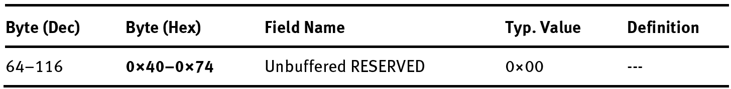
For JEDEC SPD Specification v1.0, these fields are reserved and should be set to 0×00.
For JEDEC SPD Specification v1.1, some of these fields are defined.

For v1.1 of the specification, the following bytes may be programmed.
Byte 34: Fine Offset for SDRAM Minimum Cycle Time (tCKmin)
This byte modifies the calculation of SPD Byte 12 (MTB units) with a fine correction using FTB units. The value of tCKmin comes from the SDRAM datasheet. This value is a Two’s Complement multiplier for FTB units, ranging from +127 to -128. Examples: See SPD byte 12. For Two’s Complement encoding, see Relating the MTB and FTB.
Byte 35: Fine Offset for Minimum CAS Latency Time (tAAmin)
This byte modifies the calculation of SPD Byte 16 (MTB units) with a fine correction using FTB units. The value of tAAmin comes from the SDRAM datasheet. This value is a Two’s Complement multiplier for FTB units, ranging from +127 to -128. Examples: See SPD Byte 16. For Two’s Complement encoding, see Relating the MTB and FTB.
Byte 36: Fine Offset for Minimum RAS# to CAS# Delay Time (tRCDmin)
This byte modifies the calculation of SPD Byte 18 (MTB units) with a fine correction using FTB units. The value of tRCDmin comes from the SDRAM datasheet. This value is a Two’s Complement multiplier for FTB units, ranging from +127 to -128. Examples: See SPD byte 18. For Two’s Complement encoding, see Relating the MTB and FTB.
Byte 37: Minimum Row Precharge Delay Time (tRPmin)
This byte modifies the calculation of SPD Byte 20 (MTB units) with a fine correction using FTB units. The value of tRPmin comes from the SDRAM datasheet. This value is a Two’s Complement multiplier for FTB units, ranging from +127 to -128. Examples: See SPD byte 20. For Two’s Complement encoding, see Relating the MTB and FTB.
Byte 38: Fine Offset for Minimum Active to Active/Refresh Delay Time (tRCmin)
This byte modifies the calculation of SPD Bytes 21 and 23 (MTB units) with a fine correction using FTB units. The value of tRCmin comes from the SDRAM datasheet. This value is a Two’s Complement multiplier for FTB units, ranging from +127 to -128. Examples: See SPD byte 21 and 23. For Two’s Complement encoding, see Relating the MTB and FTB.
Module-Specific Section: Bytes 60–116
This section contains SPD bytes specific to DDR3 module families. Module Type Key Byte 3 is used as an index for the encoding of bytes 60–116. The content of bytes 60–116 are described in multiple appendices, one for each memory module family.
SPD Field #60: “Module Nominal Height” Definition from JEDEC DDR3 SPD Specification
SPD Field 0×3C: (Unbuffered): Module Nominal Height
Down-on-board memory designs should set this field to 0×00.

Byte 60 (Unbuffered): Module Nominal Height
This byte defines the nominal height (A dimension) in millimeters of the fully assembled module, including heat spreaders or other added components. Refer to the relevant JEDEC JC-11 module outline (MO) documents for dimension definitions.
| Bits 7–5 | Bits 4–0 |
| Reserved | Module Nominal Height max in mm (baseline height = 15 mm) |
| Reserved | 00000 = height≤15 mm |
| 00001 = 15 < height≤16 mm | |
| 00010 = 16 < height≤17 mm | |
| 00011 = 17 < height≤18 mm | |
| 00100 = 18 < height≤19 mm | |
| ... | |
| 01010 = 24 < height≤25 mm | |
| 01011 = 25 < height≤26 mm | |
| ... | |
| 01111 = 29 < height≤30 mm | |
| 10000 = 30 < height≤31 mm | |
| ... | |
| 11111 = 45 mm<height |
SPD Field 0×3D: (Unbuffered): Module Max. Thickness
Down-on-board memory designs should set this field to 0×00.

Byte 61 (Unbuffered): Module Maximum Thickness
This byte defines the maximum thickness (E dimension) in millimeters of the fully assembled module, including heat spreaders or other added components above the module circuit board surface. Thickness of the front of the module is calculated as the E1 dimension minus the PCB thickness. Thickness of the back of the module is calculated as the E dimension minus the E1 dimension. Refer to the relevant JEDEC JC-11 module outline (MO) documents for dimension definitions.
| Bits 7–4 | Bits 3–0 |
| Module Maximum Thickness max, Back, in mm (baseline thickness = 1 mm) | Module Maximum Thickness max, Front, in mm (baseline thickness = 1 mm) |
| 0000 = thickness≤1 mm | 0000 = thickness≤1 mm |
SPD Field #61: “(Unbuffered): Module Maximum Thickness” Definition from JEDEC DDR3 SPD Specification
SPD Field 0x3E: (Unbuffered): Reference Raw Card Used
Each DIMM equivalent consists of a single rank of ×8 SDRAM devices, no ECC. This corresponds to RAW Card Version A, ×64, which would make SPD field #62=0×00.

The various Reference Raw Card Enumerators are described in this document: JEDEC Standard No. 21C: 240-Pin PC3-6400/PC3-8500/PC3-10600/PC3-12800 DDR3 SDRAM Unbuffered DIMM Design Specification, Revision 1.01, November 2009, http://www.jedec.org/ (requires account).

Byte 62 (Unbuffered): Reference Raw Card Used
This byte indicates which JEDEC reference design raw card was used as the basis for the module assembly, if any. Bits 4–0 describe the raw card and bits 6–5 describe the revision level of that raw card. Special reference raw card indicator, ZZ, is used when no JEDEC standard raw card reference design was used as the basis for the module design. Preproduction modules should be encoded as revision 0 in bits 6–5.
The JEDEC committee defines a specific “Reference Raw Card” enumerator for a given DIMM topology. The DIMM equivalents used in the design must be analyzed (number of ranks, ×4, ×8, ×16 components, ECC, and so on) and matched to the appropriate JEDEC Reference Raw Card. The matching Reference Raw Card number is put into this SPD field.
In our example topology shown below:


SPD Field #62: “(Unbuffered): Reference Card Used” Definition from JEDEC DDR3 SPD Specification
SPD Field 0×3F: Unbuff Addr. Mapping from Edge Connector to DRAM
If the motherboard has mirrored the address lines, set to 1. The typical values assume the board address mapping is standard.

Byte 63: Address Mapping from Edge Connector to DRAM
This byte describes the connection of edge connector pins for address bits to the corresponding input pins of the DDR3 SDRAMs for rank 1 only; rank 0 is always assumed to use standard mapping. Only two connection types are supported, standard or mirrored, as described in the mapping table below. System software must compensate for this mapping when issuing mode register set commands to the ranks of DDR3 SDRAMs on this module.
| Bits 7–1 | Bit 0 |
| Reserved | Rank 1 Mapping |
| Reserved | 0 = standard 1 = mirrored |
The definition of standard and mirrored address connection mapping is detailed below; highlighted rows in the table indicate which signals change between mappings.
SPD Field #63: “Address Mapping from Edge Connector to DRAM” Definition from JEDEC DDR3 SPD Specification
All reserved fields should be set to 0×00.
SPD Field 0×75 and 0×76: Module Manufacturer ID Code, LSB
Although a module is “technically” the DIMM manufacturer, it is recommended to put in the ID for the SDRAM vendor. The JEDEC specification JEP-106 contains the list of module vendors. The code for Micron Technology is 0×802C.
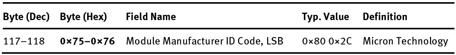
Byte 117: Module Manufacturer ID Code, Least Significant Byte
Byte 118: Module Manufacturer ID Code, Most Significant Byte
This two-byte field indicates the manufacturer of the module, encoded as follows: the first byte is the number of continuation bytes indicated in JEP- 106; the second byte is the last nonzero byte of the manufacturer’s ID code, again as indicated in JEP-106.
| Byte 118 Bits 7–0 | Byte 117 Bit 7 | Byte 117 Bits 6–0 |
| Last Nonzero Byte | Odd Parity for | Number of Continuation Codes |
| Module Manufacturer | Byte 117 bits 6–0 | Module Manufacturer |
| See JEP-106 | See JEP-106 |
Examples:

SPD Field #117 and #118: “Module Manufacture ID Code” Definition from JEDEC DDR3 SPD Specification
SPD Field 0×77: Module Manufacturer Location

Byte 119: Module Manufacturing Location
The module manufacturer includes an identifier that uniquely defines the manufacturing location of the memory module. While the SPD specification will not attempt to present a decode table for manufacturing sites, the individual manufacturer may keep track of manufacturing location and its appropriate decode represented in this byte.
SPD Field 0×78 and 0×79: Module Manufacturing Date
The current week number should be inserted into the lower byte. The last two years of the year number should be inserted into the upper byte. Make sure to use Binary Coded Decimal for the two numbers.

Bytes 120–121: Module Manufacturing Date
The module manufacturer includes a date code for the module. The JEDEC definitions for bytes 120 and 121 are year and week, respectively. These bytes must be represented in Binary Coded Decimal (BCD). For example, week 47 in year 2003 would be coded as 0×03 (0000 0011) in byte 120 and 0×47 (01000111) in byte 121.
SPD Field 0x7A–0x7D: Module Serial Number
Since there isn’t a module (DIMM) physically present, this field is a “not care.” However, it should be programmed for BIOS algorithms to be able to tell “if the DIMM has changed,” which is a trigger for fast or slow boot paths.

Bytes 122–125: Module Serial Number
The supplier must include a unique serial number for the module. The supplier may use whatever decode method desired to maintain a unique serial number for each module. One method of achieving this is by assigning a byte in the field from 122–125 as a tester ID byte and using the remaining bytes as a sequential serial number. Bytes 117–125 will then result in a 9-byte unique module identifier. Note that part number is not included in this identifier: the supplier may not give the same value for bytes 119–125 to more than one DIMM even if the DIMMs have different part numbers.
SPD Field 0×7E and 0×7F: CRC Bytes
The CRC bytes must be calculated for bytes 0–125 using the formula above. Note that
CRC needs to be checked for bytes 0–116 if bit 7 in SPD field #0 was set to 1b (which I don’t recommend). This site is very useful for calculating the CRC-16 values: http://www.lammertbies.nl/comm/info/crc-calculation.html.
The result is shown in the CRC-16 field. Make sure to remove all spaces between the bytes, and make sure to select the “Hex” option, not “ASCII.”

Bytes 126–127: SPD Cyclical Redundancy Code (CRC)
This 2-byte field contains the calculated CRC for previous bytes in the SPD. The following algorithm and data structures (shown in C) are to be followed in calculating and checking the code. Bit 7 of byte 0 indicates which bytes are covered by the CRC.

SPD Field #126 and #127: “CRC Bytes” Definition from JEDEC DDR3 SPD Specification
Since there isn’t a physical DIMM, I tend to use the SDRAM component name in lieu of the Module Part number. Also, this site is very useful for converting ASCII strings to hex values: http://easycalculation.com/ascii-hex.php.
Ensure to use the “Equivalent Hex Value” result.

Bytes 128–145: Module Part Number
The manufacturer’s part number is written in ASCII format within these bytes. Unused digits are coded as ASCII blanks (0×20).
SPD Field 0×92 and 0×93: Module Revision Code
Down-on-board memory designs should set these bytes to 0×00.

Bytes 146–147: Module Revision Code
This refers to the module revision code. While the SPD specification will not attempt to define the format for this information, the individual manufacturer may keep track of the revision code and its appropriate decode represented in this byte.
SPD Field 0×94 and 0×95: DRAM Manufacturer ID Code
Use the same value used for fields 0×75–0×76 (the SDRAM component manufacturer ID extracted from the JEP-106 JEDEC specification).

Byte 148: DRAM Manufacturer ID Code, Least Significant Byte
Byte 149: DRAM Manufacturer ID Code, Most Significant Byte
This two-byte field indicates the manufacturer of the DRAM on the module, encoded as follows: the first byte is the number of continuation bytes indicated in JEP-106; the second byte is the last non-zero byte of the manufacturer’s ID code, again as indicated in JEP-106.
| Byte 149, Bits 7–0 | Byte 148 Bit 7 | Byte 148 Bits 6–0 |
| Last Nonzero Byte, DRAM Manufacturer | Odd Parity for Byte 148 bits 6–0 | Number of Continuation Codes DRAM Manufacturer |
| See JEP-106 | See JEP-106 |
SPD Field 0×96–0×AF: Manufacturer’s Specific Data
Down-on-board memory designs should set these bytes to 0×00.

Bytes 150–175: Manufacturer’s Specific Data
The module manufacturer may include any additional information desired into the module within these locations.
SPD Field 0×B0–0×FF: Open for Customer Use
Down-on-board memory designs should set these bytes to 0×00.

Bytes 176–255: Open for Customer Use
These bytes are unused by the manufacturer and are open for customer use.
References for Appendix A
JEDEC Standard No. 21C: 240-Pin PC3-6400/PC3-8500/PC3-10600/PC3-
12800 DDR3 SDRAM Unbuffered DIMM Design Specification, Revision 1.01,
November 2009 http://www.jedec.org/ (requires account)
Standard Manufacturer’s Identification Code JEP106-I (Revision of JEP-106-H)
JULY 2000 http://www.jedec.org/ (requires account)
Annex K: Serial Presence Detect (SPD) for DDR3 SDRAM Modules SPD Revision
1.0 Release 18 JEDEC Standard No. 21-C http://www.jedec.org/ (requires account)
http://download.micron.com/pdf/datasheets/dram/ddr3/2Gb_DDR3_SDRAM.pdf
All data from the JEDEC DDR3 SPD Specification is Copyright © JEDEC. All Rights
Reserved. Reproduced with permission.
Information on JEDEC standards is current as of the date of this publication. For the most up-to-date version of JEDEC standards, visit www.jedec.org.