
3
BJT Circuits
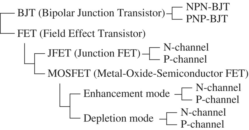
Figure 3.1 Classification of transistors.
Transistor stands for ‘transfer’ + ‘resistor’, meaning that the basic operation of a transistor is to transfer an input signal from a resistor to another resistor. Transistors are broadly classified into two groups, i.e. Bipolar Junction Transistors (BJTs) and Field Effect Transistors (FETs). The two groups of transistors are further classified as depicted in Figure 3.1.
3.1 BJT (Bipolar Junction Transistor)
The (NPN/PNP) BJT is a three‐terminal device formed from two P‐N junctions (like diodes) which share a common (P/N‐type) semiconductor and is widely used for various purposes including amplification and switching.
3.1.1 Ebers‐Moll Representation of BJT
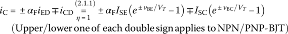
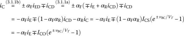
Figure 3.2(a1)/(a2), (b1)/(b2), and (c1)/(c2) shows the symbols, the basic structures, and the Ebers‐Moll models for NPN/PNP types of BJT, respectively. According to the Ebers‐Moll models, the emitter and collector currents of NPN/PNP‐BJTs are described as
where the typical values of ISE (reverse saturation current of B‐E junction) and ISC = αFISE/αR (reverse saturation current of B‐C junction) are in the order of 10−15∼10−12 and those of αF and αR are as follows:
Note that the forward and reverse saturation leakage currents are the same as each other and the transistor saturation current IS:
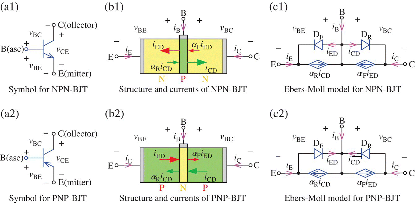
Figure 3.2 Symbols, basic structures, and models for NPN/PNP‐type Bipolar Junction Transistors (BJTs).
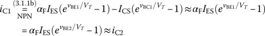
We can use these equations to write the relations between the emitter current iE and the collector current iC as
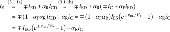
where IEO = (1 − αFαR)ISE/ICO = (1 − αFαR)ISC is the reverse emitter/collector current, which flows through the B‐E/B‐C junction when the junction is highly reverse biased and the collector/emitter terminal is open so that iC = 0/iE = 0, respectively.
Also, we can apply Kirchhoff's Current Law (KCL) to the BJT or the closed surface including its three terminals to write
Noting that the reverse emitter/collector currents IEO/ICO are negligibly small, the relationships among the three currents iC, iE, and iB of NPN‐BJT with vBE ≥ 0.7 (forward biased) and vBC < 0.4 (not forward biased enough) can be written as
According to [H-2], the collector and base currents of an NPN‐BJT can be expressed as
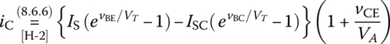
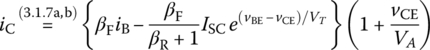
where IS = αFIES, ISC = IS/αR (typically within 10IS), and VA is the Early voltage, whose typical value is 10∼100 V. Here, compared with Eq. (3.1.1), the additional term proportional to vCE/VA has been included to account for the Early effect (also called the base‐width modulation effect) that IS increases as increasing vCE results in a decrease in the effective base width of BJT. Noting that based on these equations, the collector current iC can be expressed in terms of vCE, vBE, and iB as
we can run the following MATLAB script “plot_iC_vs_vCE.m” to plot iC versus vCE (with vBE = 0.7 V) for several values of iB as shown in Figure 3.3 where the (dotted) extrapolation of every iC curve intersects the vCE‐axis at common point vCE = −VA.
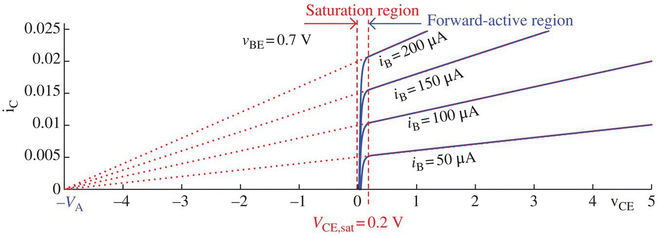
Figure 3.3 The iC‐vCE characteristic curves for different values of constant iB (with vBE = 0.7V).
3.1.2 Operation Modes (Regions) of BJT
Table 3.1 shows the four operation modes (regions) of NPN‐BJT(Si) determined by the bias conditions of B‐E and B‐C junctions. Note the following:
- When vBE = 0.7 V and vCE > 0.3 V so that vBC = vBE − vCE < 0.4, the BJT operates in the forward‐active region.
- vCE is 0.3 V at the edge of saturation and becomes vCE,sat = 0.2 V in the ‘deep’ saturation mode.
- In the forward‐active mode where vBC < 0.4, the first terms (proportional to IS) are dominant over the second terms (proportional to ISC) in Eqs. (3.1.7a) and (3.1.7b) so that iC ≈ βFiB.
- In the reverse‐active mode where vBC > 0.5, the second terms (proportional to ISC) are dominant over the first terms (proportional to IS) in Eqs. (3.1.7a) and (3.1.7b) so that iC ≈ −(βR + 1)iB. This corresponds to Eq. (3.1.6d) where the roles of the collector and emitter terminals have been switched.
3.1.3 Parameters of BJT
To analyze BJT circuits, we need to define the following parameters for the forward‐/reverse‐active mode:
Table 3.1 Operation modes (regions) of NPN–BJT (Si) with VTD = 0.5 V.
| Operation mode | Forward‐active | Cut‐off | Saturation | Reverse‐active | |
| Bias condition | B‐E | Forward (vBE ≥ VTD) | Reverse (vBE < VTD) | Forward (vBE ≥ VTD) | Reverse (vBE < 0.4) |
| B‐C | Reverse (vBC < 0.4) | Reverse (vBC < 0) | Forward (vBC ≥ 0.4) | Forward (vBC ≥ VTD) | |
| Functions | Current‐controlled current source iC = −αFiE, vBE = 0.7 V | Open switch | Closed switch vBE = 0.7 V vCE = 0.2 V | Roles of E and C terminals switched iE = −αRiC | |
- Forward‐active mode
<CE (Common‐Emitter), forward large‐signal (DC) current gain>
(3.1.9a)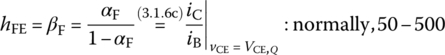
<CB (Common‐Base), forward large‐signal (DC) current gain>
<CE (Common‐Emitter), forward small‐signal (AC or incremental) current gain>
(3.1.10a)
<CB (Common‐Base), forward small‐signal (AC or incremental) current gain>
(3.1.10b)
- Reverse‐active mode
<CE (Common‐Emitter), reverse large‐signal (DC) current gain>
(3.1.11a)
<CB (Common‐Base), reverse large‐signal (DC) current gain>
(3.1.11b)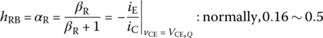
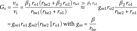
3.1.4 Common‐Base Configuration
Figure 3.4(a) shows a common‐base (CB) NPN‐BJT circuit in which the input is applied to the BEJ (B‐E junction) and the output is available from the BCJ (B‐C junction) so that the base terminal is common between the input and the output. Note that since the BEJ/BCJ are forward/reverse biased, we can expect the BJT to operate in the forward‐active mode (Table 3.1). Also, note that since the BEJ and BCJ are nonlinear resistors, we may have to apply the load line analysis for both the B‐E loop and the B‐C loop.
To perform a comparatively exact analysis considering the nonlinearity of the circuit, we draw the load line on the B‐E characteristic curve (Figure 3.4(b)) where the load line equation can be obtained by applying KVL around the B‐E loop:
The intersection of the load line with the B‐E characteristic curve is the operating (bias) point QE:
where it does not matter which one of many B‐E characteristic curves with different values of vCB is used to determine the operating point because B‐E characteristic curve varies little with vCB. Then we draw the load line on the B‐C characteristic curve (Figure 3.4(c)) where the load line equation can be obtained by applying KVL around the B‐C loop:
The intersection of the load line with the B‐C emitter characteristic curve for −iE = 9.3 mA gives the operating point QC:
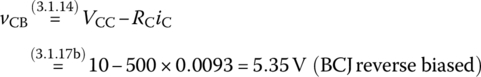
To be strict, unless the B‐E characteristic curve varies little with vCB, we should relocate QC with the B‐E characteristic curve for vCB = 5.35 V and repeat the same process iteratively. Then this theoretical analysis becomes time‐consuming even for such a simple circuit. However, as a practical means, when the BEJ (B‐E junction) is surely forward biased, we often set the BEJ voltage as
Figure 3.4 A Common‐Base (CB) BJT circuit and related v‐i characteristic curves.
and instead of performing the load line analysis for the B‐E loop, use Eqs. (3.1.12), (3.1.6c), (3.1.9b), and (3.1.14) together with βF = 186 (BETADC from the PSpice simulation output file or databook) to obtain the following:
Now, to perform the PSpice simulation, we create an OrCAD/PSpice project named, say, “CB_BJT.opj,” compose the schematic as depicted in Figure 3.4(a), make a Simulation Settings dialog box (with Bias Point analysis type) as depicted in Figure 3.4(d), and run it to get the PSpice simulation output some part of which is shown in Figure 3.4(e). The Bias Point analysis result can also be made seen in the schematic (Figure 3.4(a)) by clicking on the ‘Enable Bias Voltage Display’ and ‘Enable Bias Current Display’ buttons in the tool bar above the Schematic Editor window.
3.1.5 Common‐Emitter Configuration
Figure 3.5(a) shows a common‐emitter (CE) NPN‐BJT circuit in which the input is applied to the BEJ (B‐E junction) and the output is available from the CEJ (C‐E junction) so that the emitter terminal is common between the input and the output. Note that we can expect the BJT to operate in the forward‐active mode since the BEJ/BCJ are forward/reverse biased (Table 3.1).
To perform a comparatively exact analysis considering the nonlinearity of the circuit, we do the following:
- Setting the BEJ voltage to vBE = 0.7 V, apply KVL around the B‐E loop to find the base current iB as
- Draw the load line on the C‐E characteristic curve(s) (Figure 3.5(b)) where the load line equation can be obtained by applying KVL around the C‐E loop:
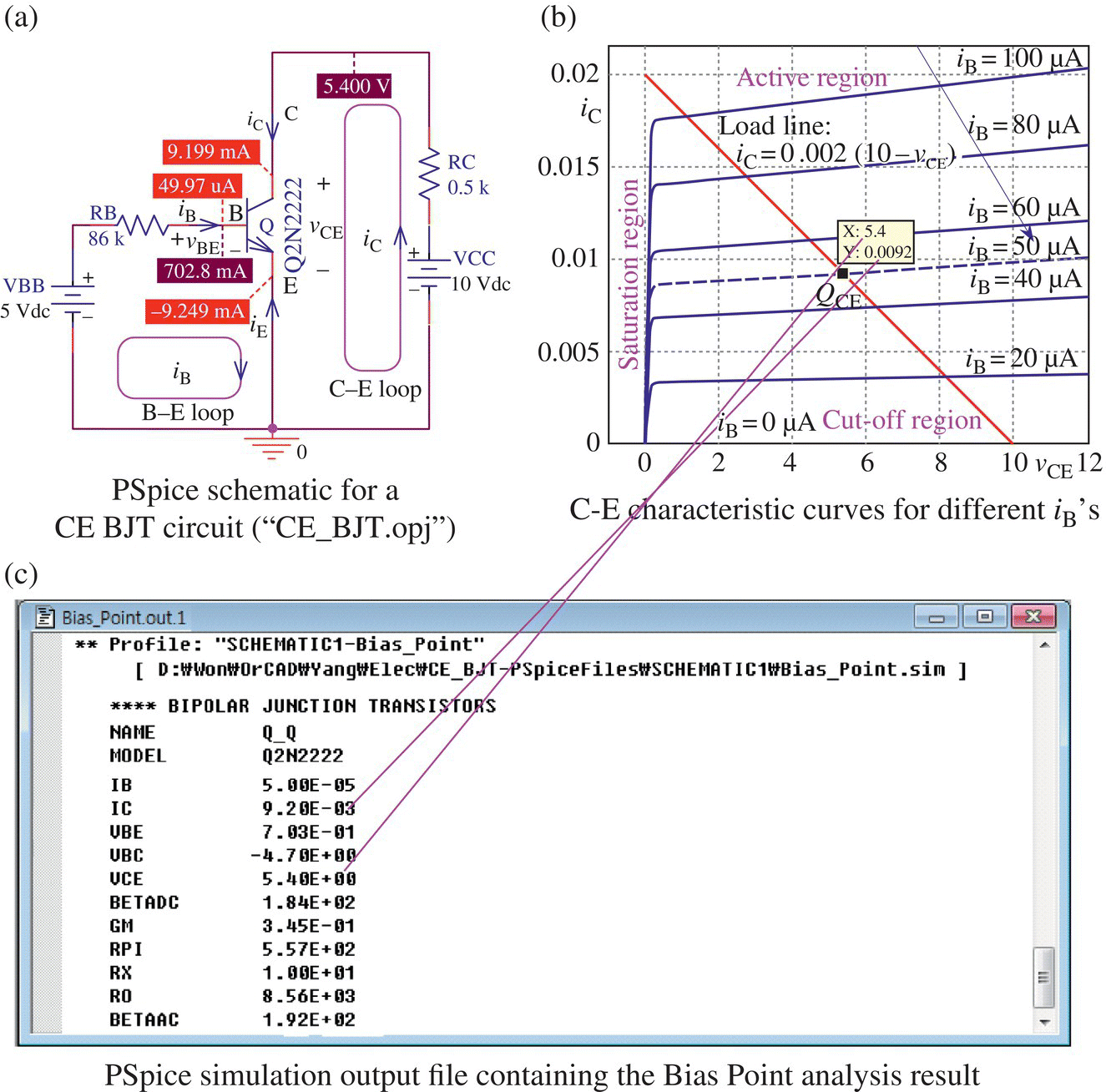
Figure 3.5 A Common‐Emitter (CE) BJT circuit and related v‐i characteristic curves.
- The intersection of the load line with the C‐E characteristic curve for iB = 50 μA gives the operating point QCE:
(3.1.20)

Most often, as a more practical means instead of the load line analysis, we use Eqs. (3.1.6c), (3.1.18), and (3.1.19) together with βF = 184 (BETADC from the PSpice simulation output file or databook) to obtain the following:
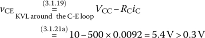
Whichever of the graphical or analytical methods we may use, we need to check if vCE > 0.3 V so that the BJT will not enter the saturation mode. If vCE turned out to be not greater than 0.3 V, then we would have to set vCE = vCE,sat = 0.2 V and use Eq. (3.1.19) to find the collector current iC.
Now, to perform the PSpice simulation, we create an OrCAD/PSpice project named, say, “CE_BJT.opj,” compose the schematic as depicted in Figure 3.5(a), make a Simulation Settings dialog box (with Bias Point analysis type) as depicted in Figure 3.4(d), and run it to get the PSpice simulation result as shown in Figure 3.5(c), which is a part of the PSpice simulation output file that can be seen by selecting View>Output_File from the top menu bar. The Bias Point analysis result can also be made seen in the schematic (Figure 3.5(a)) by clicking on the ‘Enable Bias Voltage Display’ and ‘Enable Bias Current Display’ buttons in the tool bar above the Schematic Editor window.
3.1.6 Large‐Signal (DC) Model of BJT
Figure 3.6(a)/(b)/(c)/(d) shows the large‐signal (DC) models of an NPN‐BJT for the forward‐active/saturation/reverse‐active/cut‐off modes, respectively. Figure 3.7(a) shows a typical (DC driven) BJT biasing circuit. Figure 3.7(b)/(c)/(d) shows its equivalents with the BEJ biasing side replaced by its Thevenin equivalent and with the BJT replaced by its model in the forward‐active/saturation/reverse‐active mode, respectively.
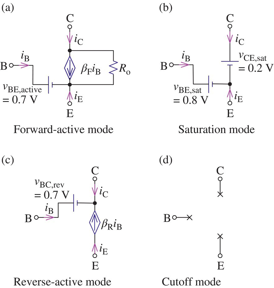
Figure 3.6 Large‐signal models of NPN‐BJT in different operation modes (regions).
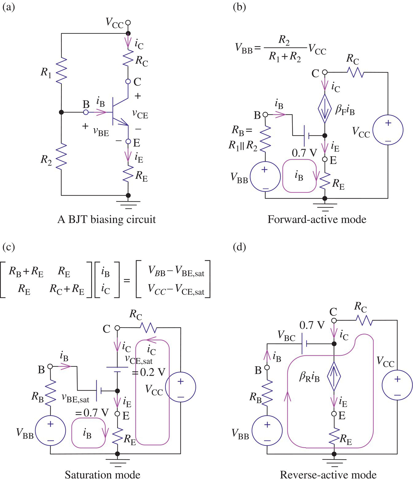
Figure 3.7 A BJT biasing circuit and its equivalents in different operation modes (regions) of BJT.
The above MATLAB function ‘BJT_DC_analysis()’ can be used to analyze NPN‐BJT biasing circuits (driven by DC sources) and find the values of VB,Q, VE,Q, VC,Q, IB,Q, IE,Q, and IC,Q (voltages/currents at/through the base, emitter, and collector terminals) at the operating point. Note the following about its usage:
- If the emitter terminal is connected (via RE) to another voltage source VEE, the first input argument should be a two‐dimensional vector [VCC VEE].
- If the base terminal is connected (via RB) to another voltage source VBB, the second and third input arguments should be VBB and RB, respectively.
Likewise, the above MATLAB function ‘BJT_PNP_DC_analysis()’ has been composed to analyze typical (DC driven) PNP‐BJT biasing circuits.
Instead of the (linear) large‐signal model as in Figure 3.6, the exponential model of an NPN‐BJT based on Eq. (3.1.7) (with VA = ∞ to exclude the Early effect) can be used to write KVL equations in vBE and vBC along the two paths VCC‐RC‐CBJ‐BEJ‐RE‐VEE and VCC‐RC‐CBJ‐RB‐VBB (for the NPN‐BJT circuit in Figure 3.8(a)) as
where
Also, KVL equations in vEB and vCB can be written along the two paths VEE‐RE‐EBJ‐BCJ‐RC‐VCC and VBB‐RB‐BCJ‐RC‐VCC (for the PNP‐BJT circuit in Figure 3.8(b)) as
where
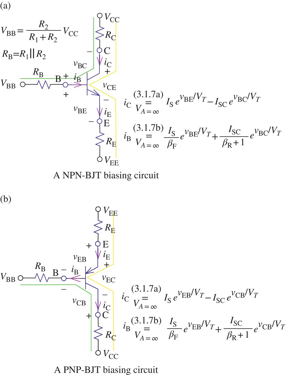
Figure 3.8 NPN/PNP BJT biasing circuits and their i‐v relations.
The following MATLAB function ‘BJT_DC_analysis_exp()’ can be used to analyze an NPN‐BJT biasing circuit (based on the exponential model) and find the values of VB,Q, VE,Q, VC,Q, IB,Q, IE,Q, and IC,Q (voltages/currents at/through the base, emitter, and collector terminals) at the operating point. Note the following about ‘BJT_DC_analysis_exp()’:
- If you want to use it for analyzing a PNP‐BJT circuit, attach the minus sign to the sixth input argument
beta. - The sixth input argument
betais expected to be given as [±βF βR IS]. - In this ‘nonlinear’ approach, active‐or‐saturated is not clear‐cut but only a matter of degree.
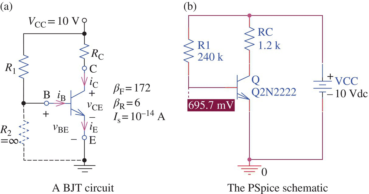
Figure 3.9 A BJT circuit and its PSpice schematic for Example 3.1.
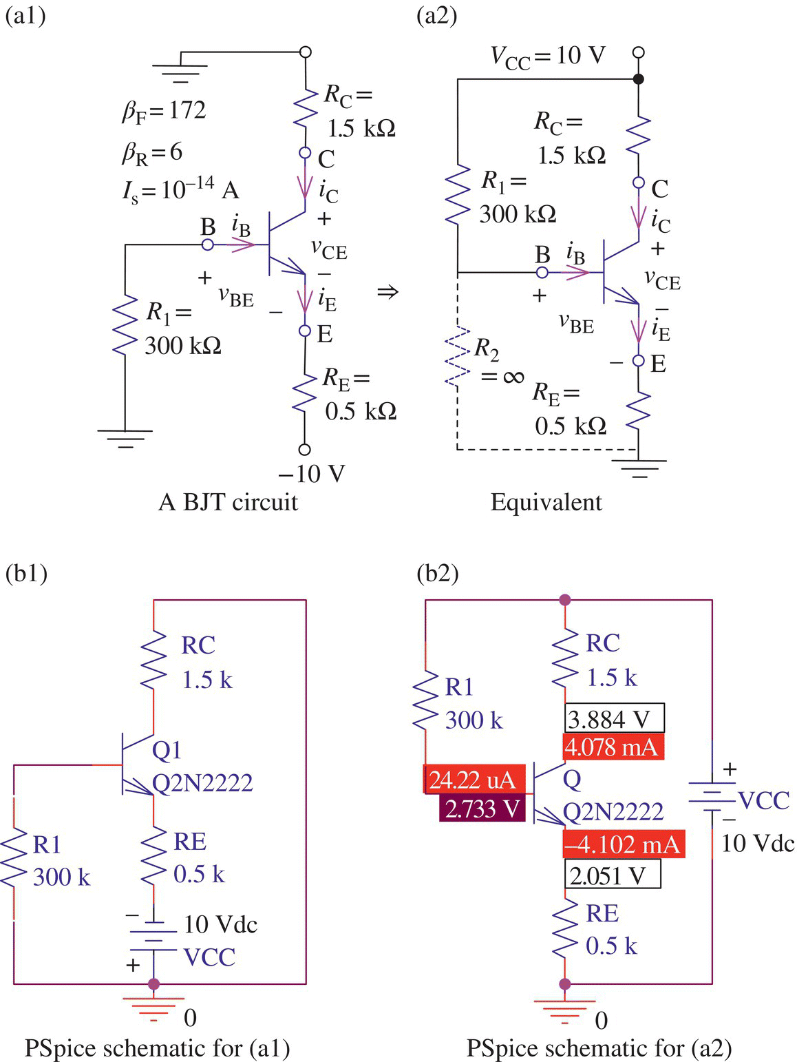
Figure 3.10 A BJT circuit, its equivalent, and their PSpice schematics for Example 3.2.
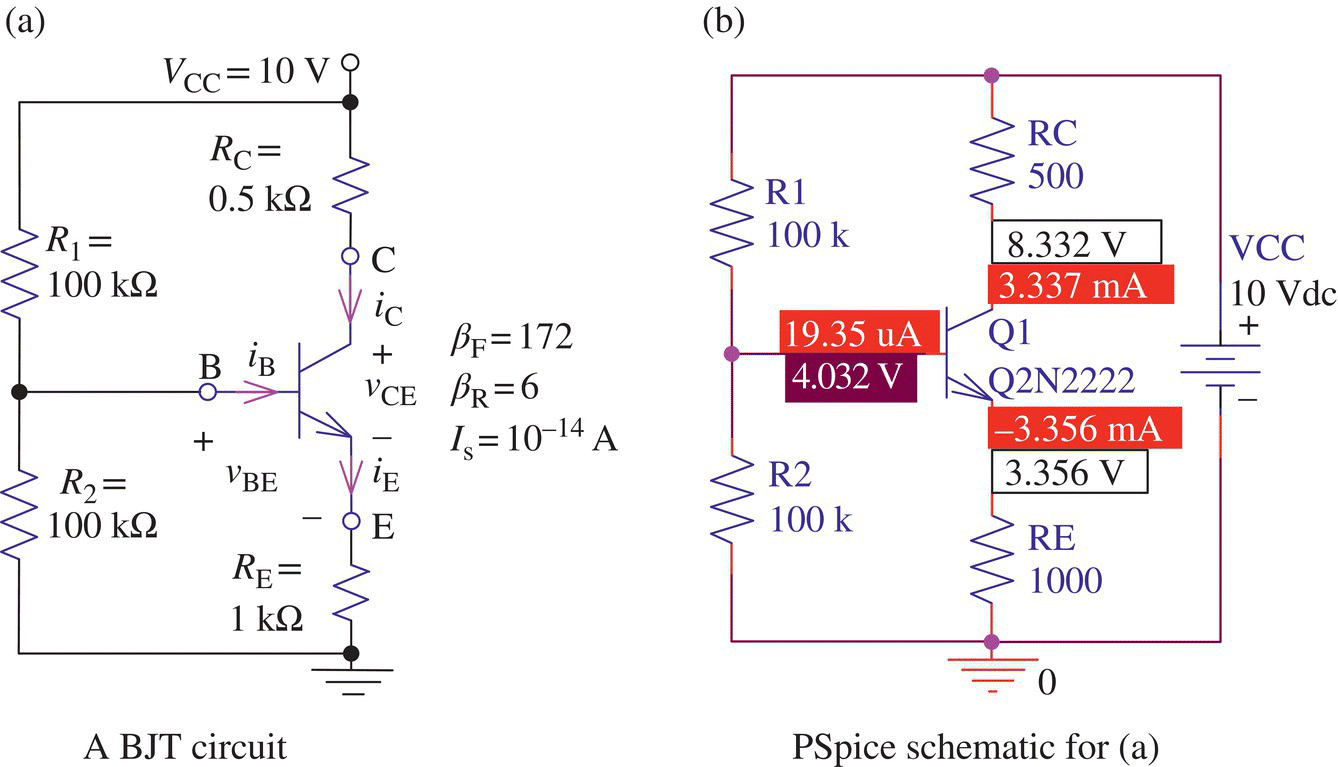
Figure 3.11 A BJT circuit and its PSpice schematic for Example 3.3.
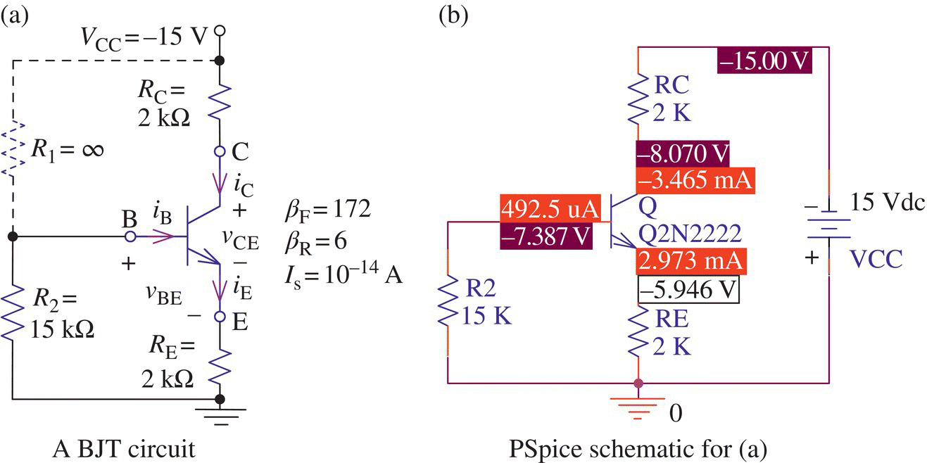
Figure 3.12 A BJT circuit and its PSpice schematic for Example 3.4.
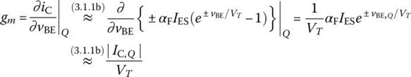
3.1.7 Small‐Signal (AC) Model of BJT
Figure 3.18(a)/(b) shows the high/low frequency small‐signal (AC) models of an NPN‐BJT for the forward‐active mode, respectively, where
- gm: transconductance (gain)
(3.1.26)
 (3.1.27)
- rb: base‐spreading resistance (40∼400 Ω)
(3.1.28)
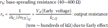
- rbc: incremental resistance of B‐C junction (several MΩ)
- Cbe (CD, Cπ, CJ E): diffusion capacitance of B‐ E junction (tens to hundreds of pF)
- Cbc (CT, Cμ, CJ
C): transition/depletion capacitance of reverse‐biased B‐
C junction (0.1∼100 pF)
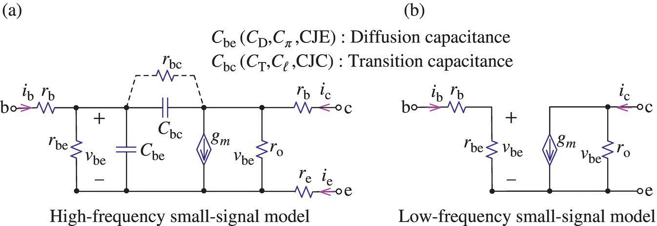
Figure 3.18 Hybrid‐π small‐signal models of NPN‐BJT with or without frequency dependence.
- Note that compared with the high‐frequency model in Figure 3.18(a), the low‐frequency model in Figure 3.18(b) has no capacitance because the magnitudes of impedance or reactance of Cbe and Cbc are large enough to be regarded as virtually open:


- Note also that referring to the low‐frequency model in Figure 3.18(b), the transconductance, gm, is related with the CE, small‐signal (AC) current gain
 as
(3.1.29)
as
(3.1.29)
3.1.8 Analysis of BJT Circuits
For the analysis of BJT circuits, the following three steps are taken where Table 3.2 shows the notations representing the DC/AC components and total solutions:
|
Table 3.2 Symbols representing DC and AC variables
| DC components at operating point Q | AC components | DC + AC components | |||
| Instantaneous values | r.m.s. values | Instantaneous values | r.m.s. values | ||
| Base current | IB,Q | ib | Ib | iB | IB |
| Voltage across C‐E junction | VCE,Q | vce | Vce | vCE | VCE |
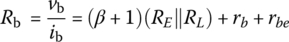
To see how the above procedure can be applied, let us consider the BJT circuit in Figure 3.19.1(a) where the roles of the three capacitors are as follows:
- Cs is used for injecting (coupling) the AC input to the base terminal of the BJT and also for blocking the DC source to keep the bias conditions undisturbed.
- CL is used for extracting the AC output signal from the collector terminal of the BJT without disturbing the DC Q‐point.
- CE is used to make the AC signal bypass RE2 so that the emitter resistance should be regarded as RE1+RE2 for setting the DC bias conditions and RE1 for producing AC output signal.
Note that Cs and CL are called coupling or blocking capacitors while CE is called a bypass capacitor. Whatever they are called, all of the capacitors are commonly supposed to provide a very large/small impedance (or reactance XC = 1/ωC) for DC(ω = 0)/AC(ω > 0) signals like being virtually open (XC = ∞)/short(XC = 0)‐circuited where ω represents the frequency of the input signal.
Now, along the procedure listed in the above box, we take the following steps:
- DC Analysis
- Remove every AC source (by open/short‐circuiting current/voltage sources) and open/short‐circuit every capacitor/inductor to find the DC equivalent circuit as shown in Figure 3.19.1(b).
- Redraw Figure 3.19.1(b) as Figure 3.19.1(c) by replacing the BEJ biasing side with its Thevenin equivalent and also replacing the BJT with its large‐signal model (Figure 3.6(b)).
- For the circuit in Figure 3.19.1(c), find the DC voltage/currents corresponding to the operating point Q where the CE, forward large‐signal (DC) current gain βF of the BJT is assumed to be 180.
(3.1.30)
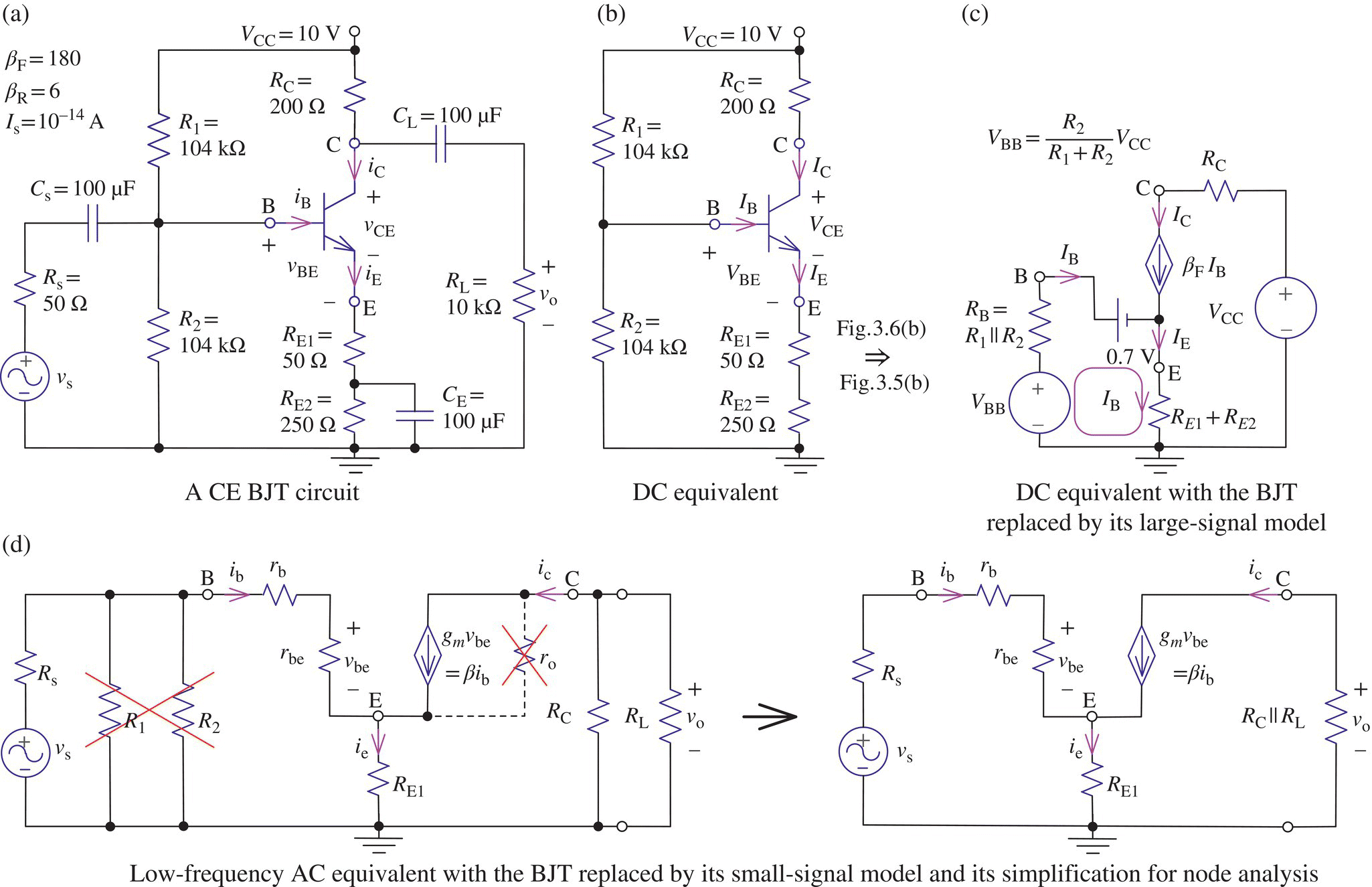
Figure 3.19.1 A CE BJT circuit and its DC/AC equivalents.
(3.1.31) (3.1.32)
 (3.1.33)
- The DC analysis can be done by running the following statements:
>>VCC=10; betaF=180; betaR=6;R1=104000; R2=104000; RC=200; RE=[50 250];BJT_DC_analysis(VCC,R1,R2,RC,RE,[betaF,betaR]);
- This yields the following results that conform with the above hand‐calculated results:
VCC VEE VBB VBQ VEQ VCQ IBQ IEQ ICQ10.00 0.00 5.00 2.90 2.20 8.54 4.05e-005 7.32e-003 7.28e-003in the forward-active mode with VCE,Q= 6.35
- AC Analysis
- Determine the small‐signal parameters such as gm, β, and rbe = rπ, ro, ….
(3.1.34) (3.1.36)
 (3.1.37)

- Remove every DC source (by open/short‐circuiting the current/voltage sources) and short/open‐circuit every (large) capacitor/inductor to find the AC equivalent circuit as Figure 3.19.1(d) where the BJT is replaced by its low‐frequency small‐signal model (Figure 3.18(b)).
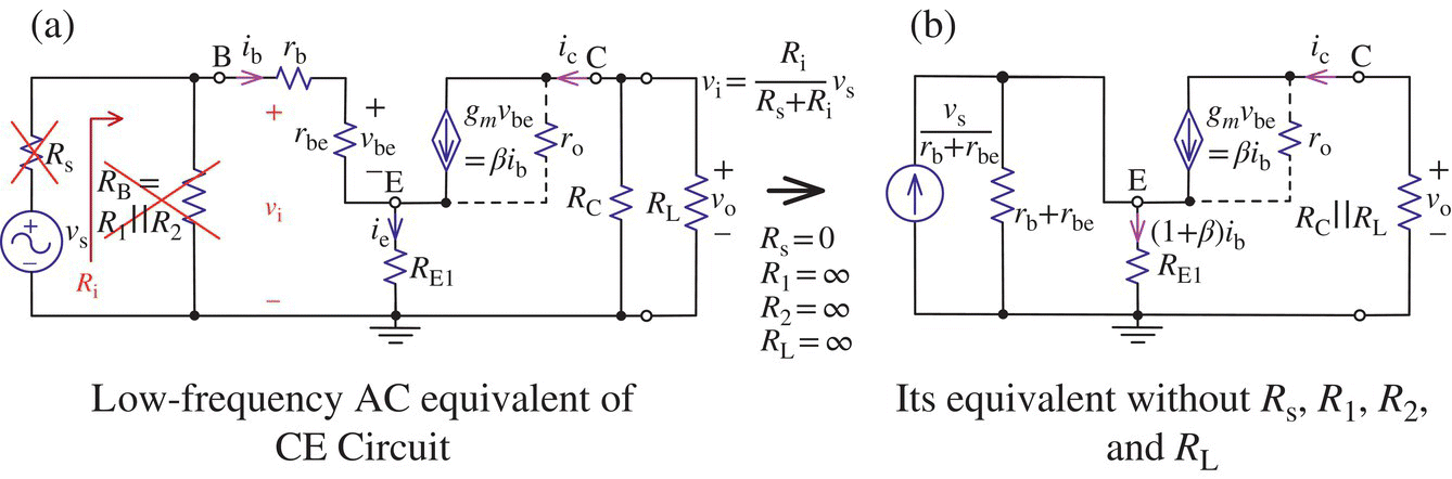
Figure 3.19.2 Low‐frequency AC equivalent without Rs, R1, R2, and RL to find the open‐loop gain Avo = vo/vi.
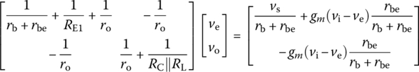
- To find the voltage gain Av=vo/vi, we remove Rs and RB=R1||R2 and then make a V‐to‐I source transformation for node analysis to get the circuit as shown in Figure 3.19.2(b).
- Then we can set up the node equation as
- In case RE1 = 0, we have just one‐node circuit and get the voltage gain as
- Once we have got the open‐loop voltage gain Avo (with RL = ∞) and the input/output resistances Ri/Ro (see Eq. (3.2.1)/(3.2.4)), we can easily get the overall voltage gain (considering Rs) as
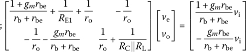
If we assume that R1, R2, and ro are so large (compared with other resistors) as to be negligible as parallel elements, we can approximate the AC equivalent as Figure 3.19.1(d) so that we can write the (small‐signal) base current ib, collector current ic, and output voltage vo as
The DC/AC analysis procedure, which has been cast into the MATLAB function ‘BJT_CE_analysis()’ listed above, can be carried out by running the following statements:
>>VCC=10; Vsm=0.02; rb=10; betaF=180; betaR=6; betaAC=194;Rs=50; R1=104000; R2=104000; RC=200; RE=[50 250]; RL=10000;BJT_CE_analysis(VCC,rb,Rs,R1,R2,RC,RE,RL,[betaF betaR betaAC],Vsm);
This yields the following result that conforms with that obtained above:
gm= 281.664[mS], rbe= 689[Ohm], ro= 1373[kOhm]Gv=Ri/(Rs+Ri)xAv = 0.994 x -3.64 = -3.62
Figure 3.20(a), (b), and (c) shows the PSpice schematic of the BJT circuit in Figure 3.19.1(a), its simulation result of the input/output voltage waveforms, and a part of simulation output file containing the netlist and the bias (operating) point information, respectively. Note that the voltage gain can be computed from the ratio between the negative/positive peak values of input/output signals shown in the Probe Cursor box as
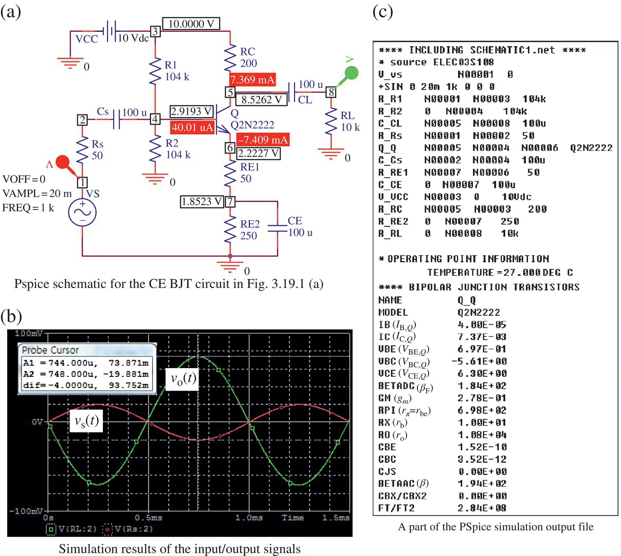
Figure 3.20 PSpice simulation of the CE BJT circuit in Figure 3.19.1a (“elec03f20.opj”).
where the negative sign indicates a phase shift of 180° between the input and the output.
Now, consider the following question:
Won’t the voltage gain and/or the linear input‐output relationship be changed when the amplitude (vsm) of the AC input voltage vs increases?
To find out the answer to this question, let us make a soft experiment of increasing vsm to 0.3 V, 1 V, and 1.5 V. The PSpice simulation results are depicted in Figure 3.21(a), (b), and (c), which show that the upper part of the output voltage waveform is distorted for vsm = 1 V and both the upper and lower parts of the output voltage waveform are distorted for vsm = 1.5 V. (This explains the meaning of ‘small‐signal’, illustrating that the small‐signal analysis result based on the linear approximation is valid only within a certain range of the input signal.) Why is that? To understand why the upper and/or lower parts of the output voltage waveform to large inputs are distorted, we should use the load line analysis by drawing the DC load line to determine the operating point Q and drawing the AC load line at the operating point Q (see Figure 3.22(a)) if there exists a (bypass) capacitor (like CE) connected in parallel with the emitter resistor RE2 (see Figure 3.19.1(a) or 3.20(a)).
Note that the equations of the DC/AC load lines are obtained by applying KVL through VCC‐RC‐vCE‐RE as
where the bypass capacitor CE is assumed to have a negligibly small reactance 1/ωCE like a short‐circuit for the input signal frequency ω and the (negative) emitter current −iE is assumed to be (almost) equal to the collector current iC since the base current is negligibly small compared with the collector/emitter currents.
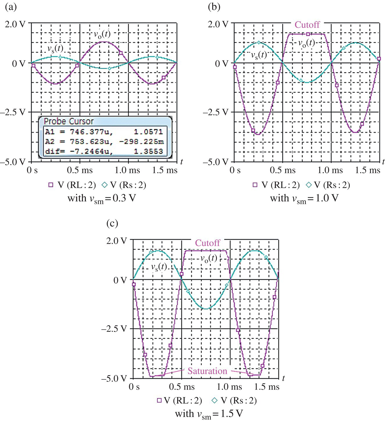
Figure 3.21 Distortion in the output voltage of the circuit of Figure 3.20a due to a large amplitude of input.
Note also that the AC input moves the instantaneous operating point along the AC load line around the quiescent operating point Q, i.e. the intersection of the DC load line and the CE characteristic curve corresponding to the base current iB determined by the DC biasing circuit. With this background knowledge, Figure 3.22(a) together with b‐d shows how iC (the collector current) and vCE (the collector‐to‐emitter voltage) vary with the variation of iB due to the AC signal. About Figure 3.22, there are several observations to make:
- A BJT crashes into the cutoff region if the amplitude of ib (the AC component of base current iB computed roughly by Eq. (3.1.41)) exceeds IB,Q so that the total base current iB = IB,Q + ib may become zero where
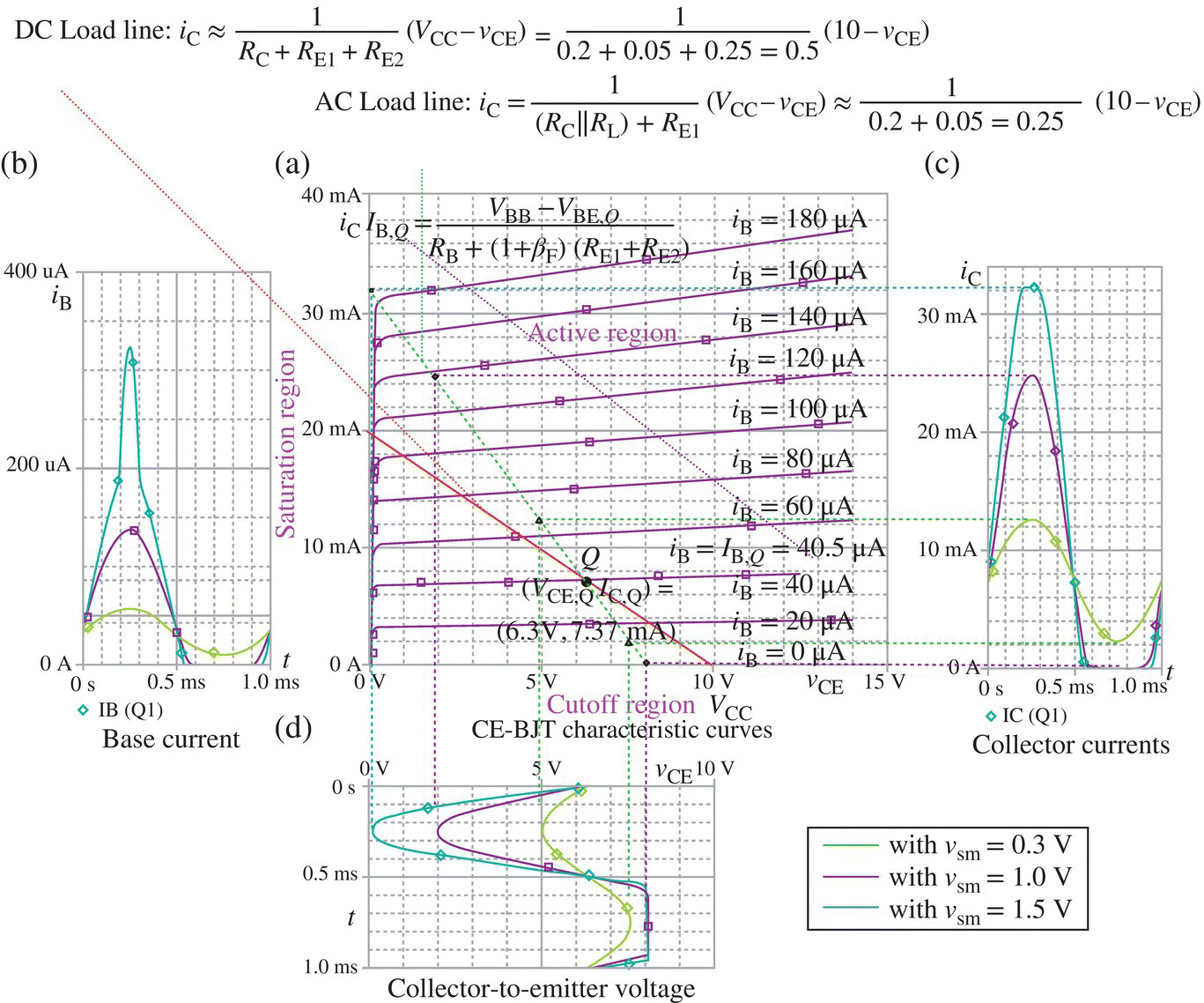
Figure 3.22 DC and AC load lines for the CE BJT circuit in Figure 3.19.1a.
(3.1.46)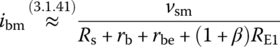
- A BJT trespasses on the saturation region if the maximum variation of vce (the AC component of collector‐to‐emitter voltage) exceeds VCE,Q−VCE,sat(0.2 V) where

- Increasing RE1 (with the voltage gain Av [Eq. (3.1.49)] decreased) reduces the DC base current

- and decreases the slope 1/(RC + RE1 + RE2) of the DC load line so that the operating point Q can move left (toward the saturation region) downwards (toward the cutoff region). However, the possibility of the BJT to trespass on the saturation region and/or crash into the cutoff region decreases because the maximum variations of vce (Eq. (3.1.47)) and ic = (β + 1)ib decrease more abruptly than the operating point Q moves left downwards.
| vsm (V) | VCC (V) | R1 (kΩ) | R2 (kΩ) | RC (Ω) | RE1 (Ω) | RE2 (Ω) | IB,Q (μA) | IC,Q (mA) | VCE,Q (V) | Remark | |
| (1) | 1.5 | 10 | 104 | 104 | 200 | 50 | 250 | 40 | 7.37 | 6.3 | Cutoff, Sat |
| (2) | 1.5 | 10 | 104 | 104 | 200 | 200 | 250 | 32.1 | 5.83 | 6.19 | Cutoff |
| (3) | 1.5 | 10 | 104 | 104 | 200 | 200 | 100 | 40 | 7.37 | 6.3 | Normal |
| (4) | 1.5 | 10 | 104 | 104 | 400 | 200 | 100 | 40.4 | 7.31 | 4.87 | Normal |
- Decreasing RE2 (with the voltage gain Av (Eq. (3.1.49)) unaffected) increases the DC base current IB,Q (Eq. (3.1.48)) and the slope 1/(RC + RE1 + RE2) of the DC load line so that the operating point Q can move right (away from the saturation region) upwards (away from the cutoff region). Thus, the possibility of the BJT to be saturated and/or cut off decreases.
- Decreasing RC decreases the maximum variation of vce (Eq. (3.1.47)) to reduce the possibility of the BJT to trespass on the saturation region, but it reduces the voltage gain

- Increasing VCC (with the voltage gain Av unaffected) increases the DC base current IB,Q (3.1.48) and pushes the vCE‐intercept rightwards so that the operating point Q can move right upwards. Thus, the possibility of the BJT to be saturated and/or cut off decreases.
The PSpice simulation results of the circuit in Figure 3.19.1(a) or 3.20(a) are depicted in Figure 3.23, which supports the observations stated above. Figure 3.23(a1)/(b1) shows the simulation results and load line analysis for the circuit with RC = 200 Ω, RE1 = 50 Ω, and RE2 = 250 Ω, respectively. Figure 3.23(a2)/(b2) shows the simulation results and load line analysis for the circuit with RC = 200 Ω, RE1 = 200 Ω, and RE2 = 250 Ω, respectively, supporting the observation that increasing RE1 (with the voltage gain Av decreased) will move the operating point Q left downwards, but will decrease the maximum variations of vce and ic more abruptly so that the possibility of the BJT to trespass on the saturation region and/or crash into the cutoff region can decrease. Figure 3.23(a3)/(b3) shows the simulation results and load line analysis for the circuit with RC = 200 Ω, RE1 = 200 Ω, and RE2 = 100 Ω, respectively, supporting the observation that decreasing RE2 (with the voltage gain Av unaffected) will move the operating point Q right upwards so that the possibility of the BJT to trespass on the saturation region and/or crash into the cutoff region can decrease. Figure 3.23(a4)/(b4) shows the simulation results and load line analysis for the circuit with RC = 400 Ω, RE1 = 200 Ω, and RE2 = 100 Ω, respectively, implying that increasing RC may increase the voltage gain Av without trespassing on the saturation region or crashing into the cutoff region thanks to the increase of linearity margin secured by increasing RE1 and decreasing RE2.
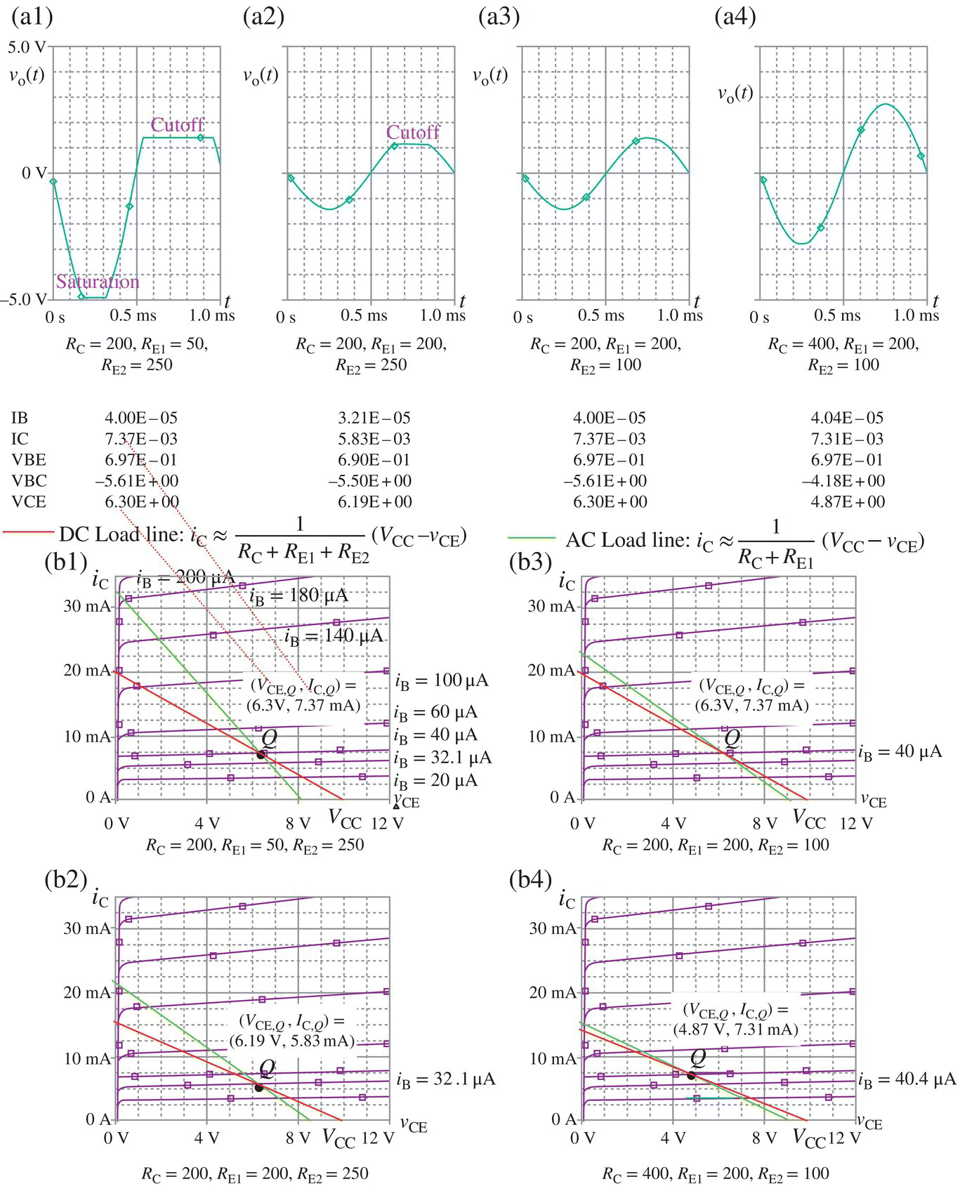
Figure 3.23 DC and AC load line for the CE BJT circuit (in Figure 3.19.1a) with different resistor values.
Can the possibility of a BJT to trespass on the saturation region or crash into the cutoff region be predicted by the MATLAB function ‘BJT_CE_analysis()’? Let us try it for the above four cases:
>>VCC=10; Vsm=1.5; rb=10; betaF=180; betaR=6; betaAC=194;Rs=50; R1=104e3; R2=104e3; RC=200; RE=[50 250]; RL=1e4; % (1)BJT_CE_analysis(VCC,rb,Rs,R1,R2,RC,RE,RL,[betaF betaR betaAC],Vsm);VCC VEE VBB VBQ VEQ VCQ IBQ IEQ ICQ10.00 0.00 5.00 2.90 2.20 8.54 4.05e-05 7.32e-03 7.28e-03in the forward-active mode with VCE,Q= 6.35gm= 281.664[mS], rbe= 689[Ohm], ro= 1373[kOhm]Possibly crash into the cutoff regionPossibly violate the saturation regionGv=Ri/(Rs+Ri)xAv = 0.994 x -3.64 = -3.62>>Rs=50; R1=104e3; R2=104e3; RC=200; RE=[200 250]; RL=1e4; % (2)BJT_CE_analysis(VCC,rb,Rs,R1,R2,RC,RE,RL,[betaF betaR betaAC],Vsm);VCC VEE VBB VBQ VEQ VCQ IBQ IEQ ICQ10.00 0.00 5.00 3.32 2.62 8.84 3.22e-05 5.83e-03 5.80e-03in the forward-active mode with VCE,Q= 6.22gm= 224.360[mS], rbe= 865[Ohm], ro= 1724[kOhm]Possibly crash into the cutoff regionGv=Ri/(Rs+Ri)xAvo = 0.998 x -0.95 = -0.95>>Rs=50; R1=104e3; R2=104e3; RC=200; RE=[200 100]; RL=1e4; % (3)BJT_CE_analysis(VCC,rb,Rs,R1,R2,RC,RE,RL,[betaF betaR betaAC],Vsm);VCC VEE VBB VBQ VEQ VCQ IBQ IEQ ICQ10.00 0.00 5.00 2.90 2.20 8.54 4.05e-05 7.32e-03 7.28e-03in the forward-active mode with VCE,Q= 6.35gm= 281.664[mS], rbe= 689[Ohm], ro= 1373[kOhm]Gv=Ri/(Rs+Ri)xAv = 0.998 x -0.96 = -0.96>>Rs=50; R1=104e3; R2=104e3; RC=400; RE=[200 100]; RL=1e4; % (4)BJT_CE_analysis(VCC,rb,Rs,R1,R2,RC,RE,RL,[betaF betaR betaAC],Vsm);VCC VEE VBB VBQ VEQ VCQ IBQ IEQ ICQ10.00 0.00 5.00 2.90 2.20 7.09 4.05e-05 7.32e-03 7.28e-03in the forward-active mode with VCE,Q= 4.89gm= 281.664[mS], rbe= 689[Ohm], ro= 1373[kOhm]Gv=Ri/(Rs+Ri)xAv = 0.998 x -1.88 = -1.88
For the four cases, the MATLAB function ‘BJT_CE_analysis()’ seems to have worked well in terms of its prediction about the possibility of the BJT to be saturated or cut off.
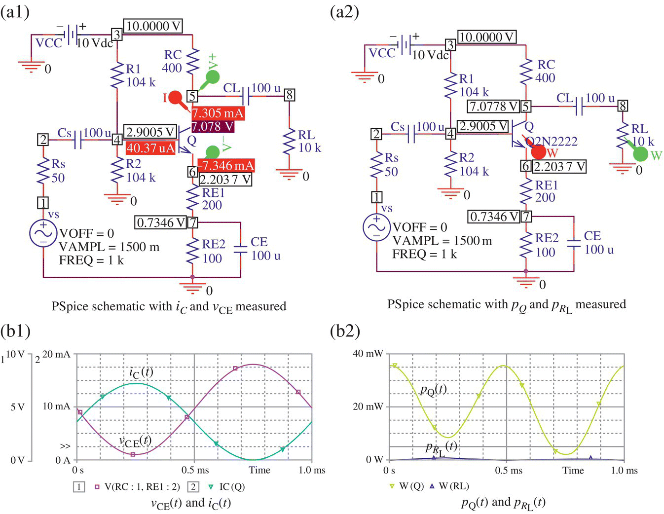
Figure 3.24 Measurement of BJT power in PSpice (“elec03f24.opj”).
Now, to find the DC power of the BJT for the last case by using MATLAB, run the following MATLAB statements:
>>[VBQ,VEQ,VCQ,IBQ,IEQ,ICQ,Av]=BJT_CE_analysis(VCC,rb,Rs,R1,R2,RC,RE,RL, [betaF betaR betaAC],Vsm);>>PQ_DC=(VCQ-VEQ)*ICQ+(VBQ-VEQ)*IBQ % DC power of BJT QPQ_DC= 0.0356 % 35.6mW
The instantaneous (DC + AC) power of the BJT can easily be found as depicted in Figure 3.24(b2) by running the PSpice schematic (Figure 3.24(a2)) with a power (W) marker placed at the center of the device. Why is the instantaneous power pQ(t) always below the DC power PQ,DC =35.6 mW of BJT? It is because vce ic < 0 (Figure 3.24(b1)) so that the AC power of the BJT is negative, implying that the BJT Q is acting as an AC source (active element) supplying an AC power to the other parts.
3.1.9 BJT Current Mirror
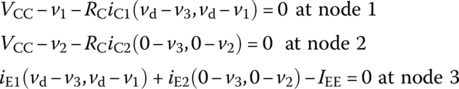
Consider the circuit of Figure 3.25(a) where the BJT Q1 is said to be diode‐connected’ or ‘connected in diode configuration’ since its collector and base terminals are short‐circuited so that it behaves like a diode. Why is a BJT used as a diode? It is for efficiency of fabricating integrated circuit (IC) with matched devices. For proper operation of the circuit, the two BJTs Q1 and Q2 must be matched in the sense that they have identical current gains (αF,βF) and characteristic curves.
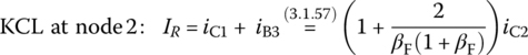
Let us analyze the circuit of Figure 3.25(a), which is called a current mirror because the currents of the two matched BJTs sharing the same vBE are equal. Assume that the voltage sources V1 and V2 forward‐bias the B‐E junctions and reverse‐bias the B‐C junctions (vBC < 0.4) of both BJTs to let them operate in the forward‐active mode so that vBE1 = vBE2 = 0.7 V and
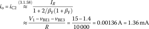
Noting that the voltage at node 1 (the lump of terminals C1‐B1‐B2) is vBE1 = 0.7 V, we apply KCL at the node to write

which yields the output current as
This is supported by the PSpice simulation result (with Bias Point analysis) listed in Figure 3.25(a), which shows that the current iC2 supplied by the current mirror is constant as about 1.4 mA for different values of V2 and, therefore, the current mirror can be used as a current source.
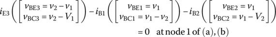
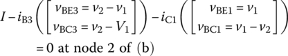
Let us analyze the circuit of Figure 3.25(b), which is also called a circuit mirror because the currents of the two matched BJTs Q1 and Q2 are equal. Assume that the voltage sources V1 and V2 forward‐bias the B‐E junctions and reverse‐bias the B‐C junctions (vBC < 0.4) of the three BJTs to let them operate in the forward‐active mode so that vBE1 = vBE2 = vBE3 = 0.7 V and
Noting that the voltage at node 1 (the lump of terminals E3‐B1‐B2) is vBE1 = 0.7 V and the voltage at node 2 (the lump of terminals C1‐B3) is vBE1 + vBE3 = 1.4 V, we can write
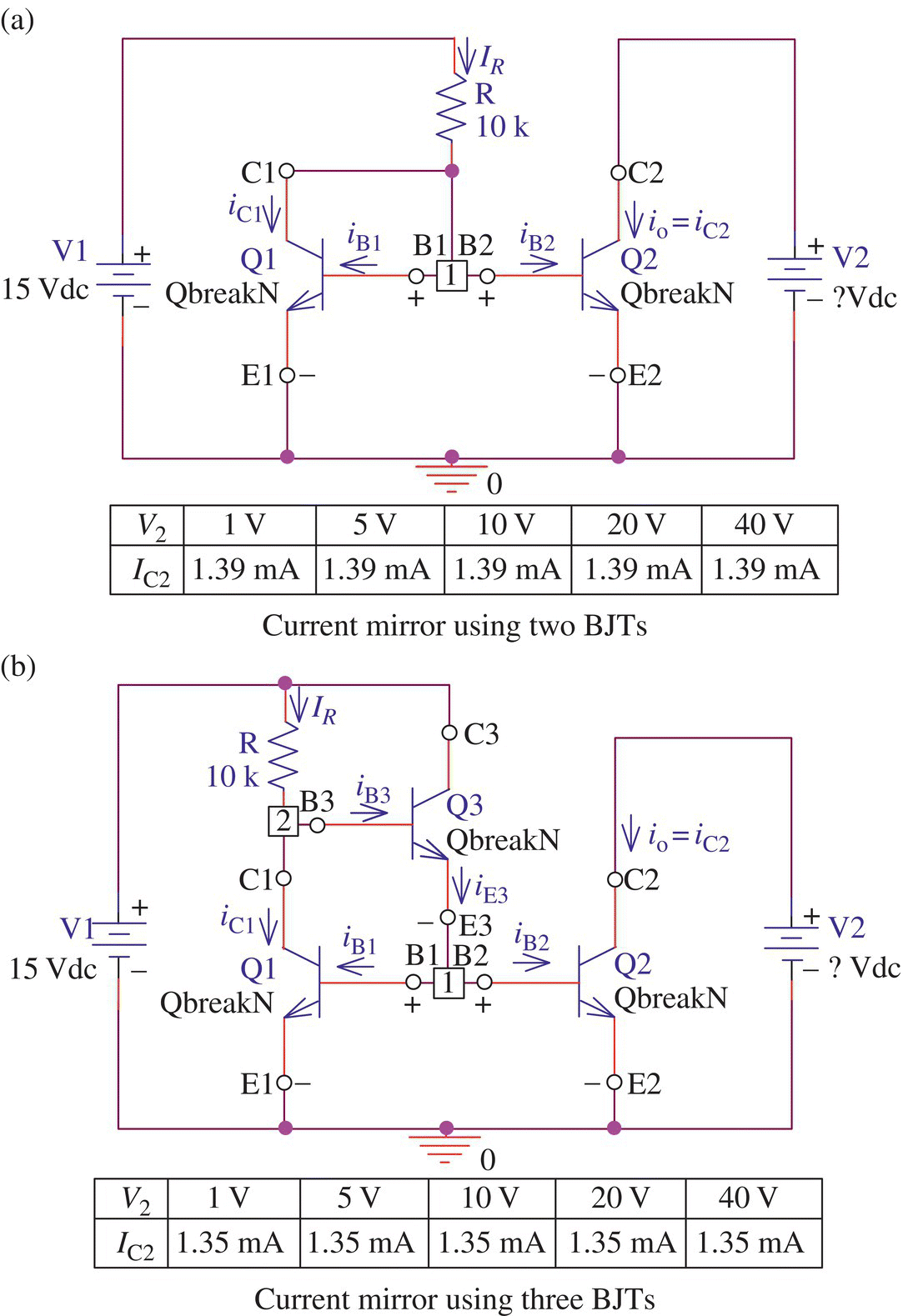
Figure 3.25 Current mirrors using BJTs (“elec03f25.opj”).
This yields the output current as
This is supported by the PSpice simulation result (with Bias Point analysis) listed in Figure 3.25(b), which shows that the current iC2 supplied by the current mirror is constant as about 1.35 mA for different values of V2 and, therefore, the current mirror can be used as a current source.
Let us compare the sensitivities of iC2 w.r.t. βF for the two current sources:

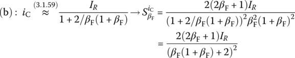
This implies that the current mirror (b) has smaller sensitivity of the output current iC2 w.r.t. βF (roughly proportional to ![]() ) compared with that of the current mirror (a) (roughly proportional to
) compared with that of the current mirror (a) (roughly proportional to ![]() ).
).
Now, to analyze the 3‐BJT current mirror (Figure 3.26(a)) and that with R replaced by a current source I (Figure 3.26(b)) by using the exponential model, we apply KCL at nodes 1 and 2 to write

where iCk(vBEk, vBCk) and iBk(vBEk, vBCk) are defined by Eqs. (3.1.23a,b), and iEk(·,·) = iBk(·,·) + iCk(·,·) for all k. The following MATLAB function ‘BJT3_current_mirror()’ solves the set of Eqs. (3.1.62a,b) for circuit (a) or Eqs. (3.1.62a,c) for circuit (b) depending on whether the value of the third input argument R is greater than or equal to 1 or not. It returns the output current io = iC2 and v = [v1 v2] for possibly several values of V2 (given as the second to last elements of the fourth input argument V12). For instance, we can solve the circuit of Figure 3.25(b) to get io for V1 = 15 V and V2 = {1, 5, 10, 20, 40} by running the following MATLAB statements:
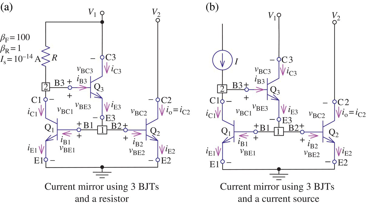
Figure 3.26 Current mirrors using a BJT as a diode.
>>R=1e4; Is=1e-14; io=BJT3_current_mirror([100 1],Is,R,[15 1 5 10 20 40])
3.1.10 BJT Inverter/Switch
Figure 3.27(a1)/(a2) shows the PSpice schematics of BJT inverter for Transient/DC_Sweep analysis. Figure 3.27(b1) shows the input and output voltage waveforms of the inverter (obtained from the Transient analysis) where the input 1(high)/0(low) drives the BJT into the saturation/cutoff mode so that the output vo = vCE can go to logic 0(low)/1(high) with high‐to‐low/low‐to‐high propagation delay tpHL/tpLH that are defined as the times between the 50% input and 50% output.
Note that in order for the BJT to go back and forth between the saturation and cutoff modes, the collector current iC,sat in the saturation mode should be less than βF times the base current iB:
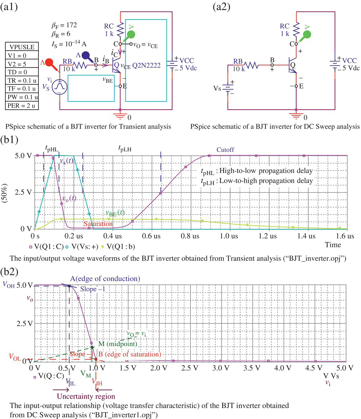
Figure 3.27 BJT inverter.
This condition can easily be satisfied by taking a small RB and a large RC. But the following should be noted:
- A small RB makes the input impedance small so that the fan‐in of the gate can be decreased where fan‐in is the number of logic gates that can be connected to its input without deteriorating the input signal or producing an undefined or incorrect output.
- A large RC makes the output impedance and loading effect (due to it) large so that the (output‐high) fan‐out of the gate can be decreased where fan‐out is the number of logic gates that can be connected to its output (as loads) without producing an undefined or incorrect output.
Figure 3.27(b2) shows the input(vi)‐output(vo) relationship, called the VTC (voltage transfer characteristic), of the inverter (obtained from the DC Sweep analysis). In the VTC, the output low/high levels VOH/VOL are defined as the minimum/maximum values of output vo corresponding to logic 1/0, respectively and VIH/VIL are defined as the minimum/maximum values of input vs that can be interpreted as logic 1/0, respectively, where VIL/VOH are the input/output at point A with slope of −1 and VIH/VOL are the input/output at point B with slope of −1. Also, we define the midpoint M as the intersection of the VTC and line vo = vi, which can be thought of as the boundary at which the inverter switches its output from one state to the other.
Figure 3.28(a) shows a practical VTC together with an ideal VTC. As measures of how much the gate can tolerate the variation of signal levels without causing any erroneous logical state, Figure 3.28(b1)/(b2) shows the high and low noise margins for practical/ideal VTCs where the high and low noise margins are defined as
What are the physical meanings of the high/low noise margins? As can be seen in Figure 3.28(b1) or (b2), the high/low noise margin means how much the high(1)/low(0) signal can decrease/increase without being mistaken for a low(0)/high(1) signal by the next‐stage (load) gate (the same kind of inverter), i.e. without misleading (mistakenly driving) the load inverter into the cutoff/saturation mode like a low/high voltage. The absolute noise margin is defined as the smaller of the two noise margins:
Note that the noise immunity measured by the absolute noise margin is maximized by the ideal VTC with abrupt switching at VIL = VIH = (VOL + VOH)/2, which has maximum logic swing from V(0) to V(1), but no transition region.
To analyze the BJT inverter circuit in Figure 3.27(a1) by using the exponential model, we can apply KVL around the two meshes to write
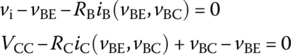
where iC(vBE, vBC) and iB(vBE, vBC) are defined by Eqs. (3.1.23a,b).
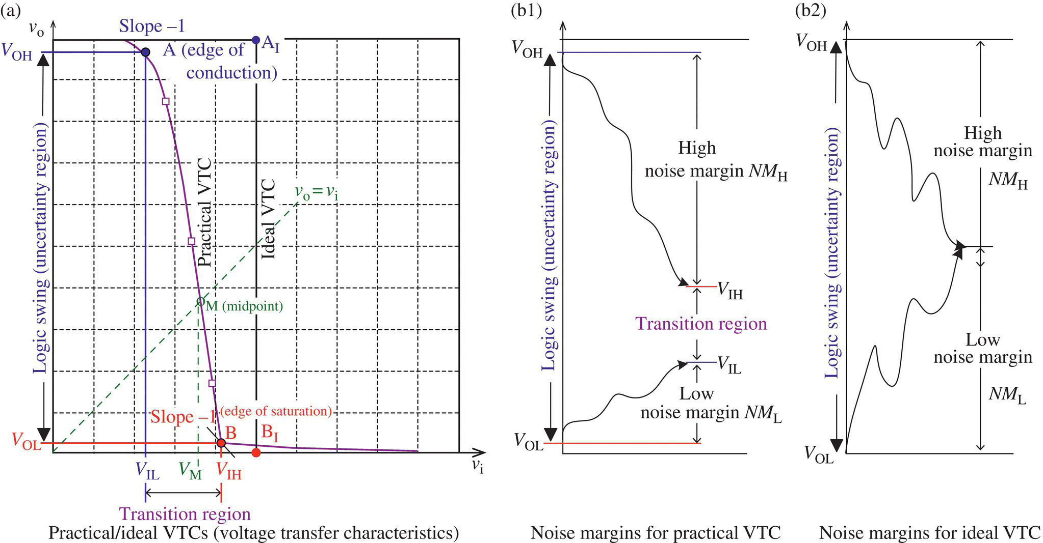
Figure 3.28 Practical/ideal voltage transfer characteristics (VTCs) and the corresponding noise margins.
Once we solve this set of equations to find vBE and vBC for a given value of the input voltage vi, we can find the output voltage vo as
The process of solving Eq. (3.1.66) to find vo for vi = 0~VCC, finding VIL,VIH,VOL, VOH, and VM, and plotting vo versus vi has been cast into the above MATLAB function ‘BJT_inverter()’. We can run the following script “plot_VTC_BJT_inverter.m” (which uses ‘BJT_inverter()’)
to get the VTC as shown in Figure 3.28(a) and the inverter parameter values as
VIL = 0.565, VIH= 0.990, VOL= 0.151, VOH= 4.971, VM= 0.920NML = 0.414, NMH= 3.981, VL = 0.031Pavg= 12.423[mW]
3.1.11 Emitter‐Coupled Differential Pair
Figure 3.29(a) shows an emitter‐coupled (in the sense that the emitter terminals of the two BJTs are connected) or differential (in the sense that its output varies with the differential input vd = vBE1 − vBE2) pair. To analyze this circuit, we assume that both BJTs operate in the forward‐active mode so that we can use Eq. (3.1.1b) to write their approximate collector/emitter currents as

Then their ratios can be approximately written as

Figure 3.29 Emitter‐coupled (differential) pair and its VTC.
Also, we apply KCL at the node E1‐E2 to write
Combining Eqs. (3.1.69) and (3.1.70) yields the expression of each collector current as

where these collector currents are depicted in Figure 3.29(b). Then we can write the (differential) output voltage as
This differential output voltage vo, together with vo1 and vo2, is shown in Figure 3.29(c). From Figure 3.29 and Eqs. (3.1.71a,b) and (3.1.72), note the following:
- If −1.5VT < vd < 1.5VT, the differential output voltage vo and other signals vary almost linearly with the differential input vd, allowing the emitter‐coupled pair to be used as an amplifier with a voltage gain of
(3.1.73)
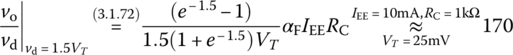
- If vd > 4VT, we have
(3.1.74a)

- On the other hand, if vd < −4VT, we have
(3.1.74b)

- It is implied that a large swing of the differential input vd = ±4VT makes the two BJTs Q1/Q2 operate as closed/open or open/closed switches, producing two distinct levels of differential output vo depending on whether vd = 4VT or vd = −4VT.
- The amplifying/switching properties are extensively used in analog/digital circuits, respectively. That is why the emitter‐coupled or differential pair is one of the most important configurations employed in ICs.
To analyze the BJT differential pair circuit in Figure 3.29(a), we can apply KCL at nodes 1, 2, and 3 to write
where iCk(vBEk, vBCk) and iBk(vBEk, vBCk) are defined by Eqs. (3.1.23a,b). The process of solving this set of equations to find v = [v1 v2 v3] for vd = −Vdm~Vdm and plotting vo = v1 − v2, iC1, iC2 (together with their analytic values computed by Eqs. (3.1.72,74) versus vd has been cast into the following MATLAB function ‘
BJT_differential()’. We can run>>betaF=100; betaR=1; Is=1e-14; IEE=10e-3; RC=1e3; VCC=12;BJT_differential([betaF betaR],Is,IEE,RC,VCC);to get the graphs of iC1, iC2, and vo as shown in Figure 3.29(b) and (c).
3.2 BJT Amplifier Circuits
This section deals with several configurations of BJT amplifier, i.e. the CE (common‐emitter) amplifier, the CC (common‐collector) amplifier (called an emitter follower), the CB (common‐base) amplifier, and cascaded or compound multistage amplifier.
3.2.1 Common‐Emitter (CE) Amplifier
Figure 3.30 shows a CE amplifier and its low‐frequency AC equivalent (which is the same as Figure 3.19.1(d)) where the BJT has been replaced by the equivalent in Figure 3.18(b), and the biasing resistances R1||R2 and BJT output resistance ro are assumed to be so large as to be negligible as parallel resistors. Let us find the input resistance, current gain, voltage gain, and output resistance.
- Input Resistance Ri
To find the input resistance, i.e. the equivalent resistance seen from the source side, we apply KVL for the left mesh (denoted in a gray closed curve) with RB = R1||R2 neglected to write

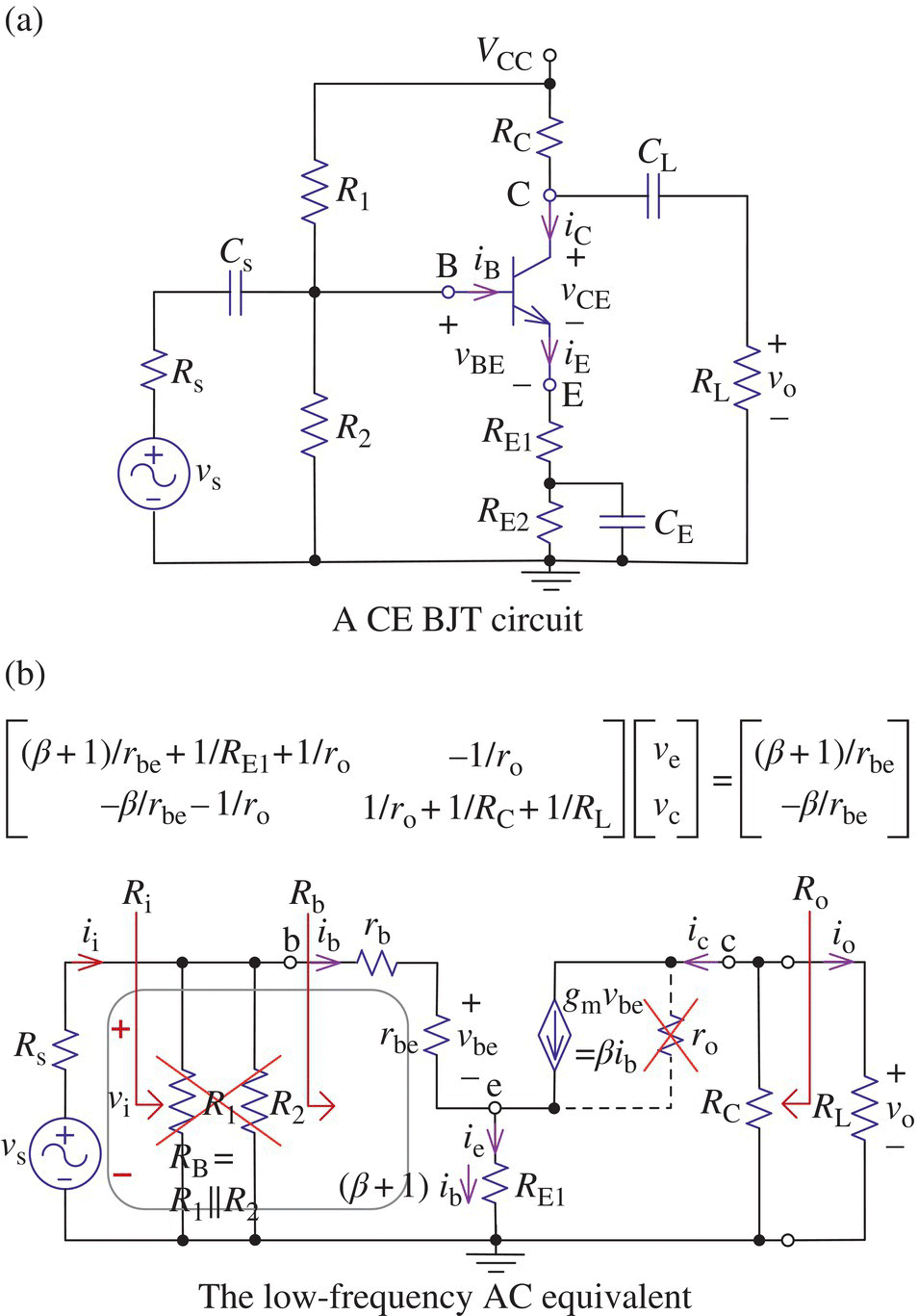
Figure 3.30 A CE (common‐emitter) BJT circuit and its low‐frequency AC equivalent.
This yields the input resistance as
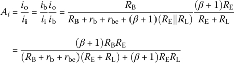
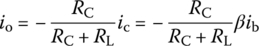
- Current Gain Ai
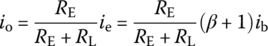
The output current io through the load resistor RL can be expressed as
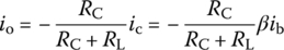
Thus, the current gain, i.e. the ratio of the output current io to the input current ii = ib is
- Voltage Gains Gvand Av
The overall voltage gain, i.e. the ratio of the output voltage vo to the source voltage vs is
- Output Resistance Ro
To find the (Thevenin) equivalent resistance seen from the load side, we need to remove the (independent) voltage source vs by short‐circuiting it. Then no current flows of itself so that we have ib = 0, vbe = 0, and ic = 0 even if a test voltage or current source is applied to the output port. Therefore, the output resistance turns out to be
This AC analysis process to find Ri, Ro, Ai, and Av has been included in the MATLAB function ‘
BJT_CE_analysis()’ presented in Section 3.1.8. If a current source supplying a BJT with its DC emitter current IE,Q is given instead of the biasing circuit as depicted in Figure 3.31(a), the following MATLAB function ‘BJT_CE_analysis_I()’ can be used for the AC analysis.
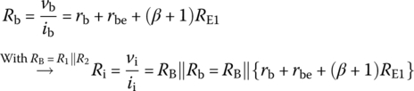
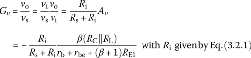
3.2.2 Common‐Collector (CC) Amplifier (Emitter Follower)
Figure 3.32 shows a CC amplifier and its low‐frequency AC equivalent where the BJT has been replaced by the equivalent in Figure 3.18(b) and the BJT output resistance ro is assumed to be so large as to be negligible as a parallel resistor. Let us find the input resistance, current gain, voltage gain, and output resistance.
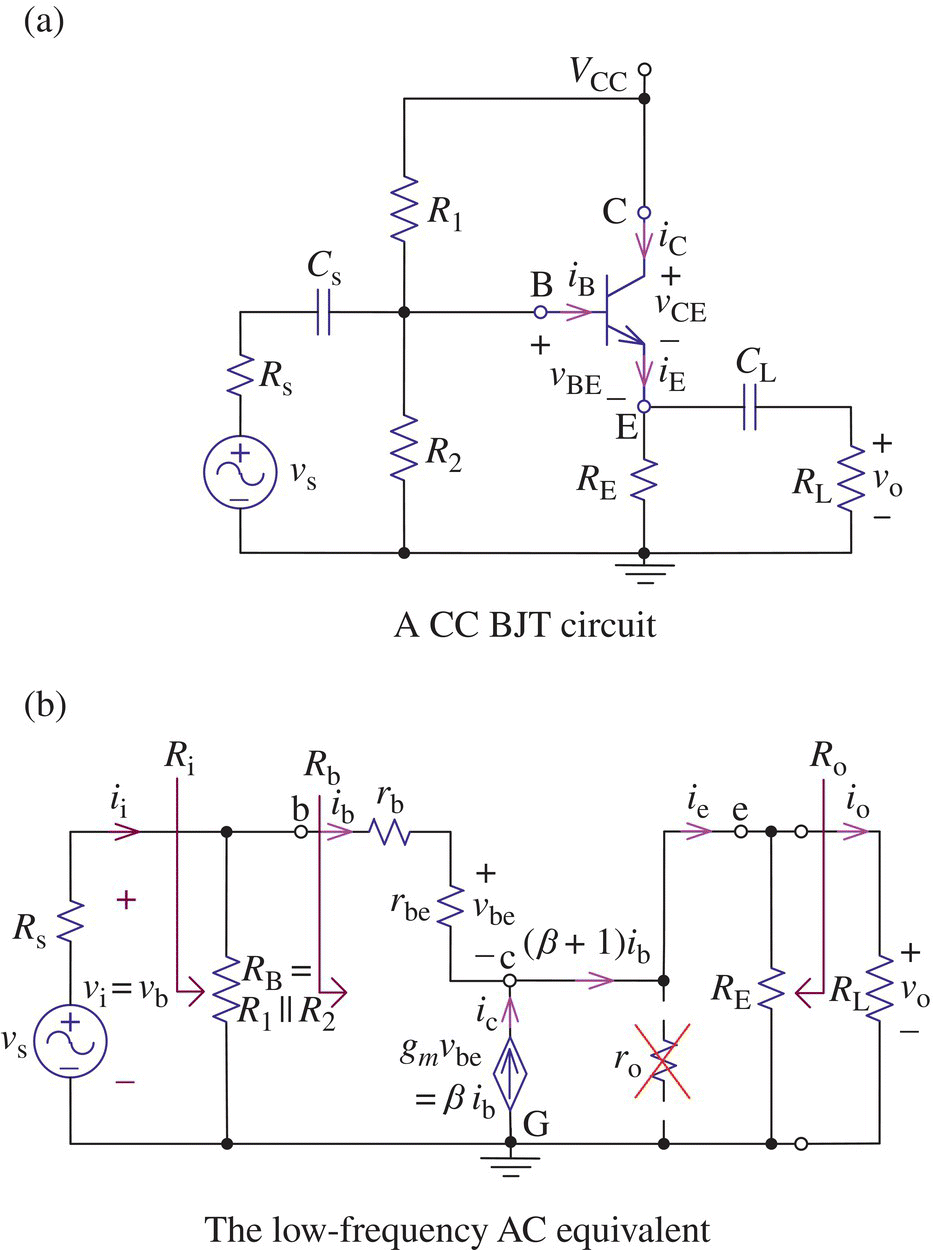
Figure 3.32 A CC (common‐collector) BJT circuit and its low‐frequency AC equivalent.
- Input Resistance Ri
To find the input resistance from the relationship between vi = vb and ii, we express the voltages at nodes e and b in terms of ib as

This yields the equivalent resistance Rb seen from terminals b‐G as
so that we can write the input resistance (including RB = R1||R2) as
- Current Gain Ai
The output current io through the load resistor RL can be expressed as
Thus, the current gain, i.e. the ratio of the output current io to the input current ii = ib is
- Voltage Gains Gvand Av
The voltage gain (with Rs = 0) is
The overall voltage gain, i.e. the ratio of the output voltage vo to the source voltage vs is
where Ri is given by Eq. (3.2.5). This implies that if Rs ≪ Ri and rb + rbe ≪ (β + 1)(RE||RL), the output voltage is almost equal to the source voltage and that is why the CC amplifier is called an emitter follower or buffer amplifier.

- Output Resistance Ro
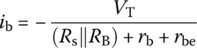
To find the (Thevenin) equivalent resistance seen from the load side, we remove the (independent) voltage source vs by short‐circuiting it and apply a test voltage source VT to the output port. Then, the base current ib and the test current IT through VT are computed as
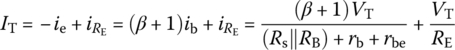
Thus, we find the output resistance as
The emitter follower has a very low output resistance (3.2.8), which enables the circuit to provide its load with much current without paying much attention to the loading effect. It also has a very high input resistance (3.2.5), which enables the circuit to save the current provided by its source (driver). In short words, the emitter follower is modest enough not to burden its source as well as generous to its load. (Isn’t the emitter follower praiseworthy? Who can blame such a nice guy for not amplifying the voltage?) That is the main feature of emitter follower with an almost unity voltage gain.
3.2.3 Common‐Base (CB) Amplifier
Figure 3.34.1 shows a CB amplifier and its low‐frequency AC equivalent where the BJT has been replaced by the equivalent in Figure 3.18(b) and the BJT output resistance ro is assumed to be so large as to be negligible as a parallel resistor. Let us find the input resistance, current gain, voltage gain, and output resistance.
- Input Resistance Ri
To find the input resistance from the relationship between vi = ve and ii, we apply KCL at node c to write
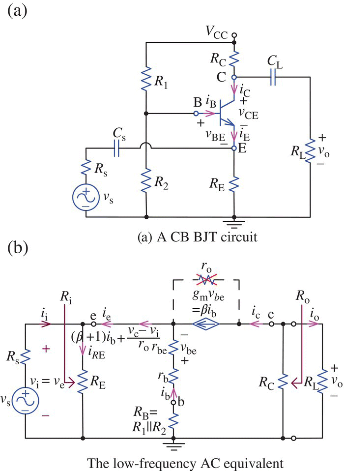
Figure 3.34.1 A CB (common‐base) BJT circuit and its low‐frequency AC equivalent.
Thus, we can find the input resistance as
This input resistance is very small compared with that (Eq. (3.2.1)) of CE amplifier and that (Eq. (3.2.5)) of CC amplifier.
- Current Gain Ai
The current
 through the emitter resistor RE can be expressed in terms of the base current ib through rbe‐rb‐RB (connected in parallel with RE) as
Applying KCL at node e yields the expression of the input current ii in terms of ib as
The output current io through the load resistor RL can be expressed as
Thus, the current gain, i.e. the ratio of the output current io to the input current ii is
- Voltage Gains Gvand Av
To find the voltage gain Av = vo/vi (with Rs = 0), we apply KCL at node c (of the circuit in Figure 3.34.1(b)) to write the node equation and solve it as
The overall voltage gain, i.e. the ratio of the output voltage vo to the source voltage vs is
where Ri is given by Eq. (3.2.9).
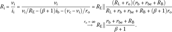
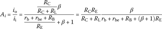
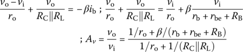
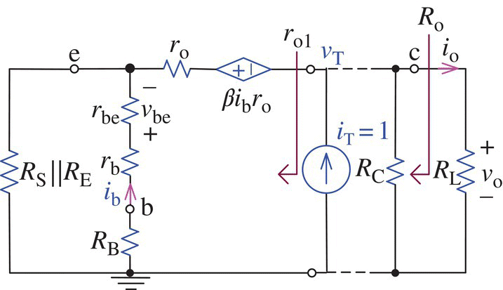
Figure 3.34.2 To find output resistance Ro of the CB circuit.
- Output Resistance Ro
To find the equivalent resistance seen from the load side, we remove the (independent) voltage source vs by short‐circuiting it, make a I‐to‐V source transformation of the dependent current source βib into the voltage source βibro in series with ro as shown in Figure 3.34.2. Then we apply a test current source of iT = 1 A and find the voltage across it:
This process for analyzing a CB amplifier to find their input/output resistances and voltage/current gains has been cast into the above MATLAB function ‘
BJT_CB_analysis()’ and the following one ‘BJT_CB_analysis_I()’ for the case where the amplifier is excited by current source.

The next section will show how the MATLAB functions presented above can be used to analyze a multistage amplifier.
3.2.4 Multistage Cascaded BJT Amplifier
Table 3.3 lists the formulas for finding the input/output resistances, voltage gain, and current gain of the CE/CC/CB amplifiers.
Note that to find the input/output resistance of a CC configuration requires the input/output resistance of the next/previous stage corresponding to its load/source resistance RL/Rs as implied by Eq. (3.2.5)/(3.2.8). That is why, for a systematic analysis of a multistage amplifier containing one or more CC configurations, we should find the input/output resistance of each stage, starting from the last/first stage backwards/forwards to the first/last stage where the load resistance to each stage except the last one is the input resistance of the next stage and the source resistance to each stage except the first one is the output resistance of the previous stage.
Table 3.3 Characteristics of Common‐Emitter/Common‐Collector/Common‐Base (CE/CC/CB) amplifiers.
| CE | CC | CB | |
| Ri | RB||{rb + rbe + (β + 1)RE1} (3.2.1) |
RB||{rb + rbe + (β+1)(RE||RL)} (3.2.5) | |
| Ro | RC||ro ≈ RC (3.2.4) | RC‖ro1 (3.2.12) | |
| Av |  (3.2.3) (3.2.3) |
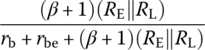 () () |
|
| Ai | 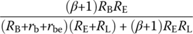 (3.2.6) (3.2.6) |
Each of the formulas listed in Table 3.3 has been coded in MATLAB as above so that they can be called individually as symbolic expressions whenever and wherever needed.
Let us consider the CE amplifier of Figure 3.36(a1) where the device parameters of the NPN‐BJT Q1 are βF = 100, βR = 1, βAC = 100, VA = 104 V, and rb = 0 Ω. Its PSpice simulation result is shown in Figure 3.36(b1) where the overall voltage gain turns out to be
Note that the theoretical value of the overall voltage gain is
This can be obtained by running the following MATLAB statements:
>>rb=0; betaF=100; betaR=1; betaAC=100;VCC=10; Vsm=0.01; beta=[betaF betaR betaAC];Rs=1e4; RL=1e3; R11=7e4; R12=3e4; RC1=5e3; RE1=[0 5e3]; Rs1=Rs; RL1=RL;BJT_CE_analysis(VCC,rb,Rs1,R11,R12,RC1,RE1,RL1,beta,Vsm);
which yields
VCC VEE VBB VBQ VEQ VCQ IBQ IEQ ICQ10.00 0.00 3.00 2.91 2.21 7.81 4.37e-06 4.42e-04 4.37e-04in the forward-active mode with VCE,Q= 5.61[V]gm= 16.915[mS], rbe= 5912[Ohm], ro= 22869.57[kOhm]Ri= 4.613 kOhm, Ro= 4999 OhmGv=Ri/(Rs+Ri)xAv= 0.316 x -14.10 = -4.45
Figure 3.36(a2) and (b2) shows a CE‐CC amplifier and its PSpice simulation result where the p‐p (peak‐to‐peak) value of the overall AC output voltage has turned out to be 20.5 times that of the AC input voltage. To analyze this multistage amplifier (containing a stage of CC configuration), we first find the input resistance of each stage, starting from the last stage backwards to the first stage:

Figure 3.36 A single‐stage amplifier of CE configuration and a two‐stage amplifier of CE‐CC configurations.
>>rb=0; betaF=100; betaR=1; betaAC=100;VCC=10; Vsm=0.01; Rs=1e4; RL=1e3; beta=[betaF betaR betaAC];R21=4e4; R22=6e4; RC2=0; RE2=5e3;% Find Ri, Av, and Ai of Stage 2/1 starting from last oneRs2=0; RL2=RL; [VBQ,VEQ,VCQ,IBQ,IEQ,ICQ,Av2,Ai2,Ri2,Ro2_0]= ...BJT_CC_analysis(VCC,rb,Rs2,R21,R22,RC2,RE2,RL2,beta);R11=7e4; R12=3e4; RC1=5e3; RE1=[0 5e3]; Rs1=Rs; RL1=Ri2; Vsm0=Vsm;[VBQ,VEQ,VCQ,IBQ,IEQ,ICQ,Av1,Ai1,Ri1,Ro1]= ...BJT_CE_analysis(VCC,rb,Rs1,R11,R12,RC1,RE1,RL1,beta,Vsm0);% Now, analyze each stage forwards from the 2nd oneRs2=Ro1; Vsm1=Ri1/(Rs+Ri1)*Av1*Vsm0[VBQ,VEQ,VCQ,IBQ,IEQ,ICQ,Av2,Ai2,Ri2,Ro2]= ...BJT_CC_analysis(VCC,rb,Rs2,R21,R22,RC2,RE2,RL2,beta,Vsm1);Vom=Av2*Vsm1, Gv = Vom/Vsm, Ri1/(Rs+Ri1)*Av1*Av2
Running these statements yields
VCC VEE VBB VBQ VEQ VCQ IBQ IEQ ICQ10.00 0.00 3.00 2.91 2.21 7.81 4.37e-06 4.42e-04 4.37e-04gm= 16.915[mS], rbe= 5912[Ohm], ro= 22869.57[kOhm] % Stage 1 of CERi= 4.613kOhm, Ro= 5912Ohm, Gv=Ri/(Rs+Ri)xAv= 0.316 x -66.79 = -21.09Vsm1 = -0.2109VCC VEE VBB VBQ VEQ VCQ IBQ IEQ ICQ10.00 0.00 6.00 5.76 5.06 10.00 1.00e-05 1.01e-03 1.00e-03gm= 38.756[mS], rbe= 2580[Ohm], ro= 9981.13[kOhm] % Stage 2 of CCRi= 18.799kOhm, Ro= 66 Ohm, Gv=Ri/(Rs+Ri)xAv= 0.79 x 0.97 = 0.77Gv = -20.4588 %Overall voltage gain of the CE-CC amplifier
This implies that the overall voltage gain of the CE‐CC stage is −20.5 (as confirmed by the PSpice simulation result Gv,s=−409.1 mV/20 mV=−20.5 in Figure 3.36(b2)), which is much greater than that (−4.45) of the CE stage (Eq. (3.2.14)) despite the additional CC stage whose voltage gain is less than one by itself.
- (Q) Why is that?
Figure 3.37(a) and (b) shows a three‐stage BJT amplifier consisting of CE‐CE‐CC configurations and its PSpice simulation result where the overall voltage gain has turned out to be Gv,s = 6.64. To analyze this multistage amplifier (containing a CC configuration), we first find the input resistance of each stage, starting from the last stage backwards to the first stage:
>>VCC=20; Vsm=5e-3; rb=0; betaF=100; betaR=1; betaAC=100; Is=1e-16;Rs=100; RL=1e4; % Source resistance and Load resistanceR31=5e4; R32=5e4; RC3=0; RE3=200; beta=[betaF,betaR,betaAC,Is];R21=1e5; R22=1e5; RC2=200; RE2=100;R11=1e5; R12=1e5; RC1=1e3; RE1=[250 50];Rs3=0; RL3=RL; [VBQ,VEQ,VCQ,IBQ,IEQ,ICQ,Av3,Ai3,Ri3,Ro3_0]= ...BJT_CC_analysis(VCC,rb,Rs3,R31,R32,RC3,RE3,RL3,beta);Rs2=0; RL2=Ri3; [VBQ,VEQ,VCQ,IBQ,IEQ,ICQ,Av2,Ai2,Ri2,Ro2_0]= ...BJT_CE_analysis(VCC,rb,Rs2,R21,R22,RC2,RE2,RL2,beta);Rs1=Rs; RL1=Ri2; Vsm0=Vsm;[VBQ,VEQ,VCQ,IBQ,IEQ,ICQ,Av1,Ai1,Ri1,Ro1]= ...BJT_CE_analysis(VCC,rb,Rs1,R11,R12,RC1,RE1,RL1,beta,Vsm0);
Figure 3.37 A three‐stage cascaded BJT amplifier and its PSpice simulation (“ce:ce:cc.opj”).
where the load resistance RL and the input resistances Ri3/Ri2 of stage 3/2 have been put as the load resistances of stage 3 and 2/1, successively and respectively. Note that 0 has been put as the third input argument (corresponding to Rs3/Rs2) of ‘BJT_CC_analysis()’/‘BJT_CE_analysis()’ for stage 3/2 because their source or input resistances are not yet known. That is why the output resistance of the CC stage (to be computed by Eq. (3.2.8) depending on Rs) is not expected to have been found properly. However, the source resistance Rs has properly been put as the third input argument of ‘BJT_CE_analysis()’ for stage 1. Running the above MATLAB statements yields the following:
Result of provisional analysis for Stage 3VCC VEE VBB VBQ VEQ VCQ IBQ IEQ ICQ20.00 0.00 10.00 4.94 4.09 20.00 2.02e-04 2.04e-02 2.02e-02in the forward-active mode with VCE,Q= 15.91[V]where beta_forced = ICQ/IBQ = 100.00 where beta = 100.00gm= 782.947[mS], rbe= 128[Ohm], ro= 494.07[kOhm]Ri= 11.088[kOhm], Ro= 1[Ohm]Gv=Ri/(Rs+Ri)xAv= 1.000x 0.99 = 0.99 % Not yet meaningfulResult of provisional analysis for Stage 2VCC VEE VBB VBQ VEQ VCQ IBQ IEQ ICQ20.00 0.00 10.00 2.38 1.54 16.95 1.52e-04 1.54e-02 1.52e-02in the forward-active mode with VCE,Q= 15.41[V]where beta_forced = ICQ/IBQ = 100.00 where beta = 100.00gm= 589.311[mS], rbe= 170[Ohm], ro= 656.42[kOhm]Ri= 8.520[kOhm], Ro= 200[Ohm]Gv=Ri/(Rs+Ri)xAv= 1.000x -1.91 = -1.91 % Not yet meaningfulResults of analysis for Stage 1VCC VEE VBB VBQ VEQ VCQ IBQ IEQ ICQ20.00 0.00 10.00 4.29 3.46 8.59 1.14e-04 1.15e-02 1.14e-02in the forward-active mode with VCE,Q= 5.13[V]where beta_forced = ICQ/IBQ = 100.00 where beta = 100.00gm= 441.426[mS], rbe= 227[Ohm], ro= 876.33[kOhm]Ri= 16.877[kOhm], Ro= 999[Ohm]Gv=Ri/(Rs+Ri)xAv= 0.994x -3.51 = -3.49
Then, to find the overall voltage gain, we multiply the product of the voltage gains of every stage with the voltage gain of the front voltage divider as
>>Gv=Ri1/(Rs+Ri1)*Av1*Av2*Av3ans = 6.6374
How close this is to the PSpice simulation result (6.63) shown in Figure 3.37(b)!
Now, to find the output resistance of the last stage of CC, starting from the first stage forwards to the last stage, we use ‘BJT_CE_analysis()’ (with Rs1 = Rs and RL1 = Ri2), ‘BJT_CE_analysis()’ (with Rs2 = Ro1 and RL2 = Ri3), and ‘BJT_CC_analysis()e’ (with Rs3 = Ro2 and RL3 = RL) for stage 1, 2, and 3, respectively. Here, the analysis of stage 1 does not have to be repeated since it has already been taken care of above.
>>Rs2=Ro1; RL2=Ri3; Vsm1=Av1*Vsm;[VBQ,VEQ,VCQ,IBQ,IEQ,ICQ,Av2,Ai2,Ri2,Ro2]= ...BJT_CE_analysis(VCC,rb,Rs2,R21,R22,RC2,RE2,RL2,beta,Vsm1);Rs3=Ro2; RL3=RL; Vsm2=Av2*Vsm1;BJT_CC_analysis(VCC,rb,Rs3,R31,R32,RC3,RE3,RL3,beta,Vsm2);
These MATLAB statements can be run to yield the following:
Results of analysis for Stage 2Ri= 8.520[kOhm], Ro= 200[Ohm]Results of analysis for Stage 3Ri= 11.088 kOhm, Ro= 3 Ohm
All the above MATLAB statements have been put into the MATLAB function ‘CE_CE_CC()’ so that it can be run by typing the following at the MATLAB prompt:
>>Rs=100; RL=1e4; Vsm=5e-3; VCC=20;[Gv,Avs,Ais,Ris,Ros]=CE_CE_CC(Rs,RL,Vsm,VCC)
Note the following about it:
- The BJT parameters such as rb(rb), βF(betaF), βR(betaR), βAC(betaAC), and Is have been set to the default values of Qbreak that can be read from the PSpice simulation output file.
- First, to find the input resistances of stage 3(CC), stage 2(CE), and stage 1(CE) (that will be load resistance to their previous stages), ‘
BJT_CC_analysis()’, ‘BJT_CE_analysis()’, and ‘BJT_CE_analysis()’ with their third/eigth input arguments Rs3=0/RL3=RL, Rs2=0/RL2=Ri3, and Rs1=Rs/RL1=Ri2, respectively, have been run backwards starting from the last stage. Then the overall voltage gain can be computed as above. - To get the proper values of Ro2 and Ro3, each stage (starting from the second one) is analyzed forwards by running the corresponding analysis function with the third/eigth input argument Rs2=Ro1/RL2=Ri3 and Rs3=Ro2/RL3=RL, respectively.
The hand calculations to find the input/output resistances can be done as follows:
Figure 3.38 shows the PSpice simulation result for measuring the overall output resistance Ro3, which yields the measured value of Ro3 as 10/2.7951 = 3.58 Ω.
Now, let us consider what will happen if we remove the third stage of CC (emitter follower) configuration to make a two‐stage amplifier as depicted in Figure 3.39(a). Then the output voltage across RL = 100 kΩ will become a bit higher as depicted in Figure 3.39(b1), which can be thought of as a natural result from omitting the CC stage with voltage gain Av3 = 0.98 < 1. However, will we have a similar result even for a smaller load resistor like RL = 100 Ω? To our surprise, the PSpice simulation result for RL = 100 Ω depicted in Figure 3.39(b2) shows that the output voltage of the two‐stage amplifier has become much lower than that of the three‐stage amplifier, which reveals the potential value of the CC stage. What is the strength of the CC stage to reduce the loading effect so that the voltage drop due to a larger load (with smaller resistance) can be very small? It is the large input resistance and the small output resistance of CC stage compared with those of CE stage as mentioned in Section 3.2.2. That is why we are willing to pay the extra cost of equipping an amplifier with a CC stage as the last one even if it may lower the output voltage a bit for a normal load.
Figure 3.38 PSpice schematic and its simulation for measuring the overall output resistance.
Figure 3.39 A two‐stage BJT amplifier and its PSpice simulation results (“ce:ce.opj”).
To use MATLAB for showing the strength of CC stage, we can compose the following MATLAB function ‘CE_CE()’ with RL as an input argument, which analyzes the two‐stage amplifier consisting of CE‐CE stages. Then we run it and the above MATLAB function ‘CE_CE_CC()’ with RL = 100:
>>Rs=100; RL=100; Vsm=0.01; VCC=20;Gv1=CE_CE(Rs,RL,Vsm,VCC), Gv2=CE_CE_CC(Rs,RL,Vsm,VCC)
which yields
Gv1 = 2.2669 Gv2 = 6.4350
This shows that as the load becomes larger, i.e. as RL becomes smaller, the role of a CC stage to reduce the loading effect becomes more remarkable.
3.2.5 Composite/Compound Multi‐Stage BJT Amplifier
- CC‐CE (Darlington) Amplifier
Figure 3.40(a)/(b) shows CC‐CE (Darlington) amplifiers using two NPN/PNP BJTs, respectively. The amplifiers can be used to achieve a large current gain since the overall output current is the sum of the two BJT collector currents:
(3.2.17)
- CC‐CC (Darlington) Amplifier
Figure 3.40(c) shows a CC‐CC (Darlington) amplifier using two NPN BJTs. This amplifier can also be used to achieve a large current gain since the overall output current is the emitter current of the second BJT:
(3.2.18)
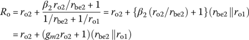
- CE‐CB (Cascode) Amplifier
Figure 3.40(d) shows a CE‐CB (cascode) amplifier using two NPN BJTs. Its output current and output voltage across the collector resistor RC are
(3.2.19)
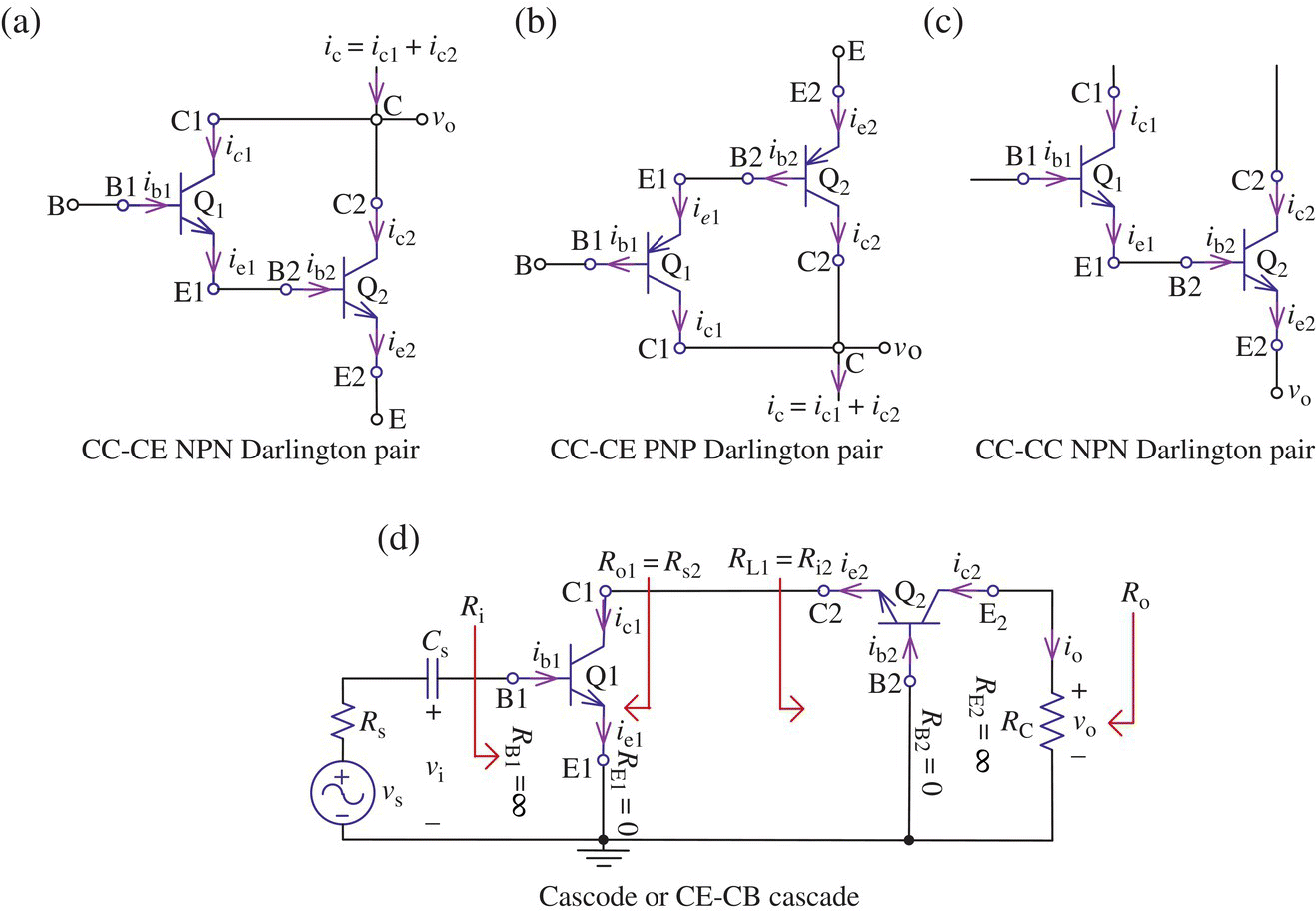
Figure 3.40 Various compound (composite) BJT amplifier circuits.
(3.2.20)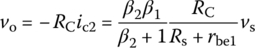
Thus, the current/voltage gains are
(3.2.21)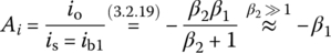
Not only the voltage/current gains but also the input/output resistances are close to those of the CE amplifier (with RE = 0, RB = ∞, and RC in place of RC||RL) discussed in Section 3.2.1. Then what is the additional BJT for? Compared with the single‐stage CE amplifier, the load resistance of the first CE stage is the input resistance of the second CB stage, which is so small that the possibility of Q1 to enter the saturation region can be reduced. That is one of the advantages that we gain from the additional (second) BJT.
It may be interesting and convenient to use the MATLAB functions listed above for deriving, say, Eq. (3.2.22) (the voltage gain of the CE‐CB (cascode) amplifier shown in Figure 3.40(d)) as follows:
>>syms b b1 b2 ro ro1 ro2 rbe rbe1 rbe2 Rs RB RC RE RLRi2=subs(Ri_CB,{b,rbe,RB,RE},{b2,rbe2,0,inf})%Input resistance from lastRi1=subs(Ri_CE,{rbe,RB,RE},{rbe1,inf,0})Ro1=subs(Ro_CE,RC,inf); % Output resistance from the first stageRo2=subs(Ro_CB,{b,rbe,Rs,RB,RE},{b2,rbe2,Ro1,0,inf})Av1=subs(Av_CE,{b,rbe,RC,RE,RL},{b1,rbe1,inf,0,Ri2})Av2=subs(Av_CB,{b,rbe,RB,RE,RL},{b2,rbe2,0,inf,inf})Ri=Ri1; Ro=Ro2; % Overall input and output resistancesGv=Ri/(Rs+Ri1)*Av1*Av2where the output resistance Ro1 of stage 1 (CE) has been put as the source resistance Rs2 of stage 2 (CB) to find the output resistance Ro2 of stage 2 and the input resistance Ri2 of stage 2 has been put as the load resistance RL1 of stage 1 to find the voltage gain Av1 of stage 1. Running these statements yields the overall input/output resistances and voltage gain as
Ri1 = rbe1 % The input resistance of the first stageRo2 = RC % The output resistance of the last stageGv = -(RC*b1*b2)/((Rs + rbe1)*(b2 + 1)) % see Eq. (3.2.22)This result conforms with Eq. (3.2.22). On the other hand, if we consider the (internal) output resistance ro (due to the Early effect) of each BJT, we can run the following statements:
>>Ri2=subs(Ri_CB(1),{b,ro,rbe,RB,RE,RL},{b2,ro2,rbe2,0,inf,inf})Ri=limit(limit(limit(subs(Ri_CE(1),rbe,rbe1),RB,inf),RC,inf),RE,0)Ro1=subs(Ro_CE(1),{ro,RC},{ro1,inf});Ro=subs(Ro_CB(1),{b,ro,rbe,Rs,RB,RC,RE},{b2,ro2,rbe2,Ro1,0,inf,inf})Av1=limit(limit(subs(Av_CE(1),{b,ro,rbe},{b1,ro1,rbe1}),RL,Ri2),RE,0)Av2=subs(Av_CB(1),{b,ro,rbe,RB,RE,RL},{b2,ro2,rbe2,0,inf,inf})Gv=Av1*Av2; % Overall voltage gain with Rs=0Gvo=limit(Gv,RC,inf); % Overall onen-loop voltage gain with RC=infpretty(simplify(Gvo))to get the overall input/output resistances and voltage gain of the CE‐CB amplifier with Rs = 0 and RC = ∞ (open) as
Ri = rbe1Ro = ro2 + ((b2*ro2)/rbe2 + 1)/(1/rbe2 + 1/ro1)b1 ro1 (rbe2 + b2 ro2)- - - - - - - - - - - - - - -% comparable to the results in Sec. 7.5.6 of [S-2]rbe1 (rbe2 + ro1)This implies

Note that 1 has been put as the first input argument of the MATLAB functions such as ‘
Ri_CB()’ to include the effect of ro. Note also that the MATLAB function ‘limit()’ is more useful than ‘subs()’ for substituting a zero or an infinity into a complicated MATLAB expression.
Note that to remove a resistance in the formulas for Ri, Ro, Av, … due to its nonexistence in a circuit, it is enough to set its value to 0/∞ if it is series-/parallel-combined with other resistance(s) without having to compare the circuit with the corresponding model in Fig. 3.30/3.32/3.34.1.
3.3 Logic Gates Using Diodes/Transistors[C-3, M-1]
This section will discuss the DTL (Diode‐Transistor Logic) NAND gate, TTL (Transistor‐Transistor Logic) NAND gate, and ECL (Emitter‐Coupled Logic) OR/NOR gate.
3.3.1 DTL NAND Gate
Figure 3.45 shows a basic DTL NAND gate consisting of a diode AND gate cascaded with a BJT inverter where the binary inputs vi1 and vi2 are supposed to be one of the two voltage levels corresponding to low (logic 0) and high (logic 1):
Let us look over several aspects of the DTL NAND gate.
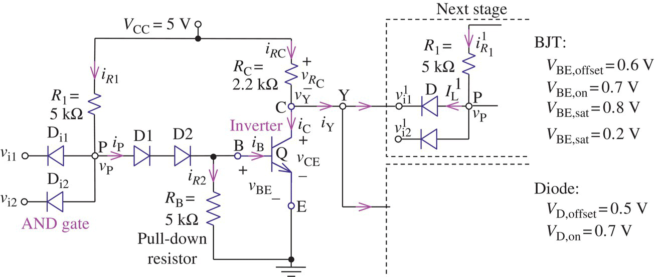
Figure 3.45 A basic DTL (Diode‐Transistor Logic) NAND gate.
- Logic Function
To check if the circuit operates as a NAND gate, let us consider the following two cases:
- At least one of the two inputs vi1 and vi2 is low as V(0)=VCE,sat=0.2 V.
- Both of the two inputs vi1 and vi2 are high as V(1)=VCC=5 V.
- Fan‐out
When the output voltage is low, i.e. vY = VCE,sat = 0.2 V with the BJT Q (in the current stage) saturated, it can let the input diode of a load gate (connected to the output node Y) forward‐biased so that the current through R1 of a load gate (in the next stage)
(3.3.16)
can flow back (sink) into the BJT Q of the current stage in addition to the existing collector current (Eq. (3.3.11)) coming through RC. Therefore, if the number of similar load gates connected to the output node Y is N, the maximum collector current of Q will be
From the condition that this maximum collector current should be less than βFiB in order to keep Q saturated, we can determine the output‐low fan‐out of the basic NAND gate as the minimum integer satisfying the above inequality (3.3.17):
How about the output‐high fan‐out of the DTL gate? When the output is high, it can let the input diodes of the load gates reverse‐biased and then the additional current flowing through RC and going into the next stage is just the sum of the reverse leakage currents that is not so large as to put a limitation on the fan‐out.
- Role of the Pull‐down Resistor RB
If there were no connection through RB between node B and ground so that iRB = 0, the base current iB = iR1 − iRB would be larger so that the fan‐out determined by Eq. (3.3.18) could be increased. Then, what is the pull‐down resistor RB for? Its role is to decrease the turn‐off time (saturation‐to‐cutoff switching time) by providing another path (in parallel with the BE junction of Q) for the reverse base current so that excess minority carriers can be removed quickly from the base while Q enters the cutoff mode from the saturation mode. Note that a smaller value of the pull‐down resistor RB makes the turn‐off time shorter, but on the other hand, it decreases the base current iB = iR1− iRB, reducing the driving capability (measured by fan‐out).
- Voltage Transfer Characteristic (VTC) and Noise Margin
Table 3.4 and Figure 3.46 show the (piecewise linear) VTC of the DTL NAND gate depicted in Figure 3.45. Figure 3.46 also shows the low/high noise margins NML/NMH defined as the maximum widths of the range in which the input voltage can vary without changing the high/low output voltage. Note that the (dotted) VTC for the gate using only one diode between nodes P and B implies that saving one diode results in a considerable reduction of the low noise margin NML.
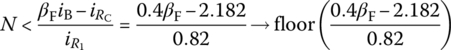
Table 3.4 Voltage transfer characteristic (VTC) of a DTL NAND gate.
| Region | Range of vi [V] | vP [V] | vB [V] | D1‐D2 | Q | vY [V] |
| 1 | 0∼0.5 = |
vi + VD, on 0.7∼1.2 |
0 | OFF | Cutoff | 5.0 |
| 2 | 0.5∼1.3 = |
vi + VD, on 1.2∼2.0 |
0∼0.5 | OFF | Cutoff | 5.0 |
| 3 | 1.3∼1.7 = |
vi + VD, on~VD, offset 2.0∼2.2 | 0.5∼0.8 | ON | Forward‐active | 5.0–0.2 |
| 4 | 1.7∼5.0 | VBE, sat + 2VD, on 2.2 V |
0.8 | ON | Saturated | 0.2 |
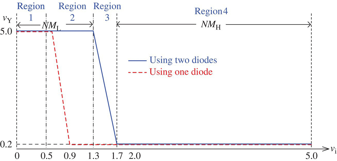
Figure 3.46 Voltage transfer characteristic of a DTL NAND gate.
3.3.2 TTL NAND Gate
3.3.2.1 Basic TTL NAND Gate Using Two BJTs
Figure 3.47 shows a basic TTL NAND gate using two BJTs where the multiple BEJs (BE junctions) of BJT Q1 replace the input diodes and the BCJ (BC junction) of BJT Q1 replaces the diode D1 of the DTL NAND gate. Note that the input clamping diodes are placed to keep the input voltages from going below −0.7 V so that Q1 can be protected from any large negative input voltage.
To check if the circuit operates as a NAND gate, let the forward/reverse DC current gains be
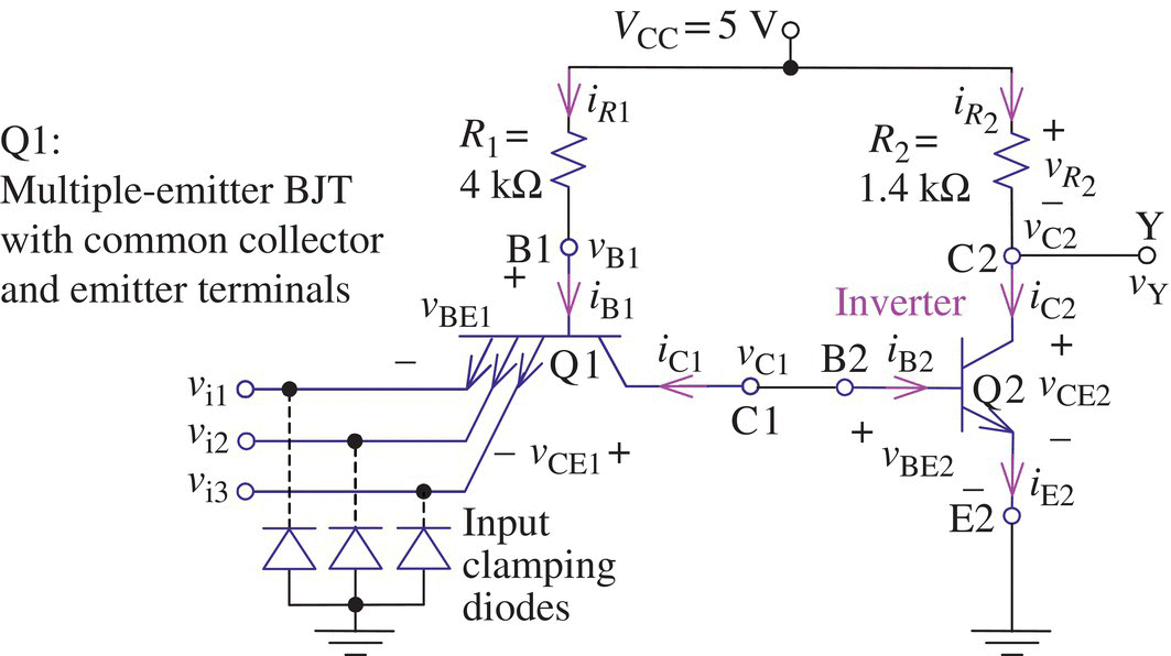
Figure 3.47 A basic TTL (Transistor‐Transistor Logic) NAND gate using two BJTs.
respectively, and consider the following two cases:
- At least one of the inputs is low as V(0) = VCE,sat = 0.2 V.
- All the inputs are high as V(1) = VCC = 5 V.
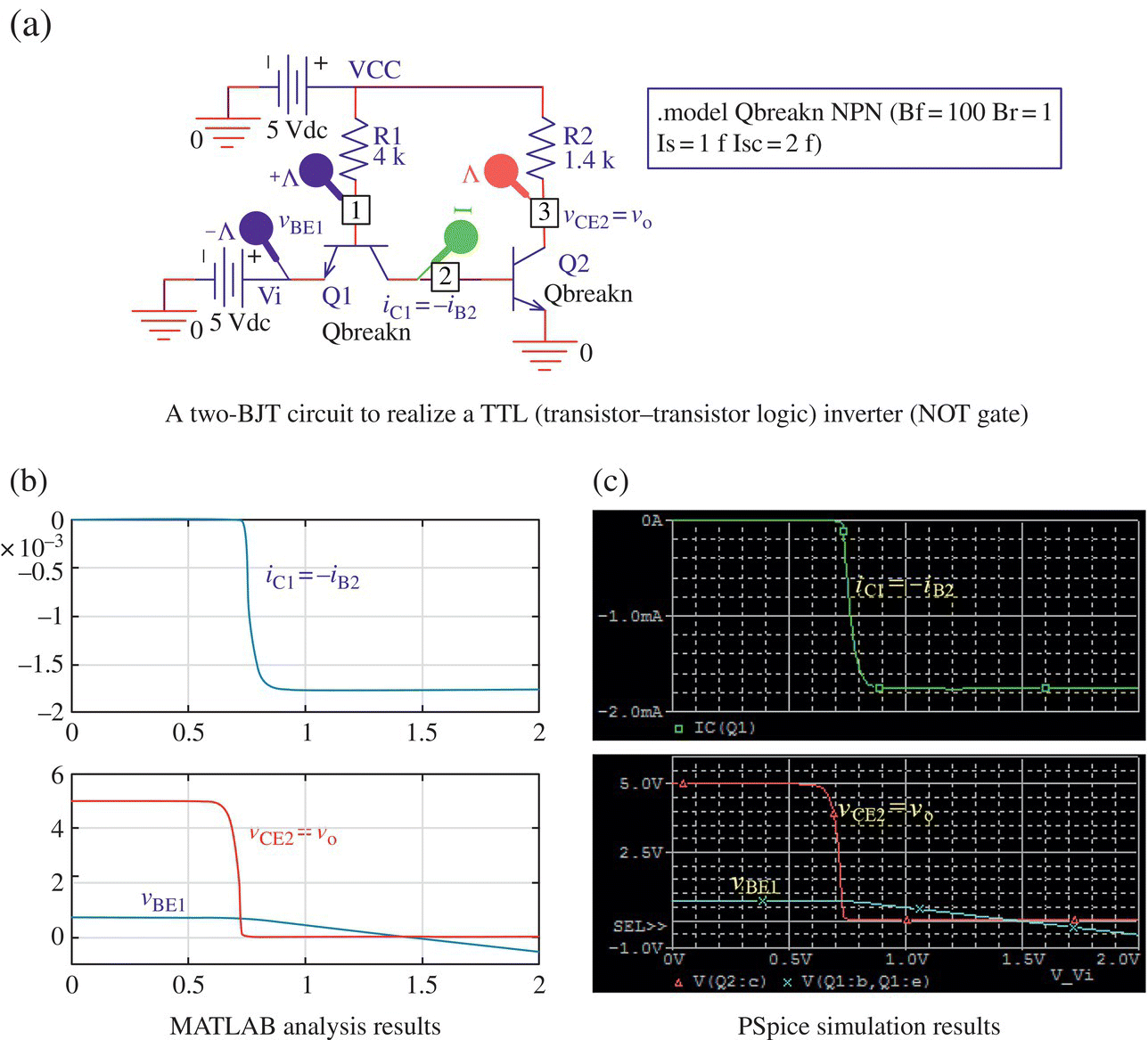
Figure 3.48 A logic inverter consisting of two BJTs and its MATLAB analysis & PSpice simulation.
3.3.2.2 TTL NAND Gate Using Three BJTs
Figure 3.49 shows a TTL NAND gate using three BJTs where compared with the basic TTL NAND gate of Figure 3.47, Q3 increases not only the fan‐out (by raising the overall current gain) but also the noise margin since the BEJ of Q3 provides an additional diode offset voltage (like D2 in the TTL NAND gate). Let us look over several aspects of the TTL NAND gate.
- Logic Function
To check if the gate operates as a NAND gate, let us consider the following two cases:
- At least one of the inputs is low as V(0) = VCE,sat = 0.2 V.
- All the inputs are high as V(1) = VCC = 5 V.
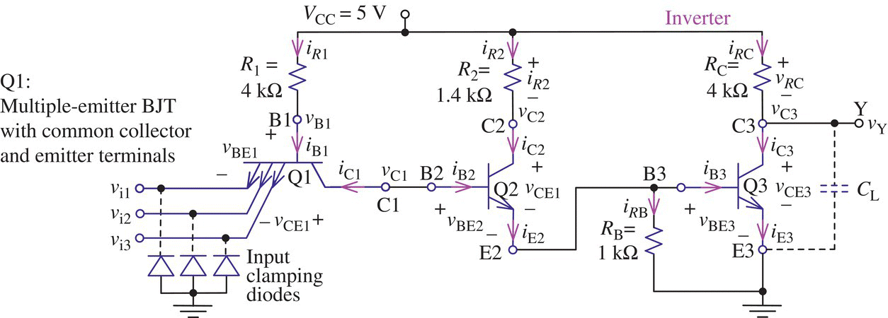
Figure 3.49 A TTL NAND gate using three BJTs.
- Output‐high Fan‐out
In Figure 3.50, suppose the output voltage of the driver gate is high, i.e. vY = VCC = 5 V with Q2 and Q3 cutoff, which can drive the BJTs
 (connected to the output node Y),
  , and
, and  of the load gate (in the next stage) into the reverse‐active, saturation, and saturation modes, respectively. Then the load current (flowing into the load gate) equal to the emitter current of
  can be obtained as
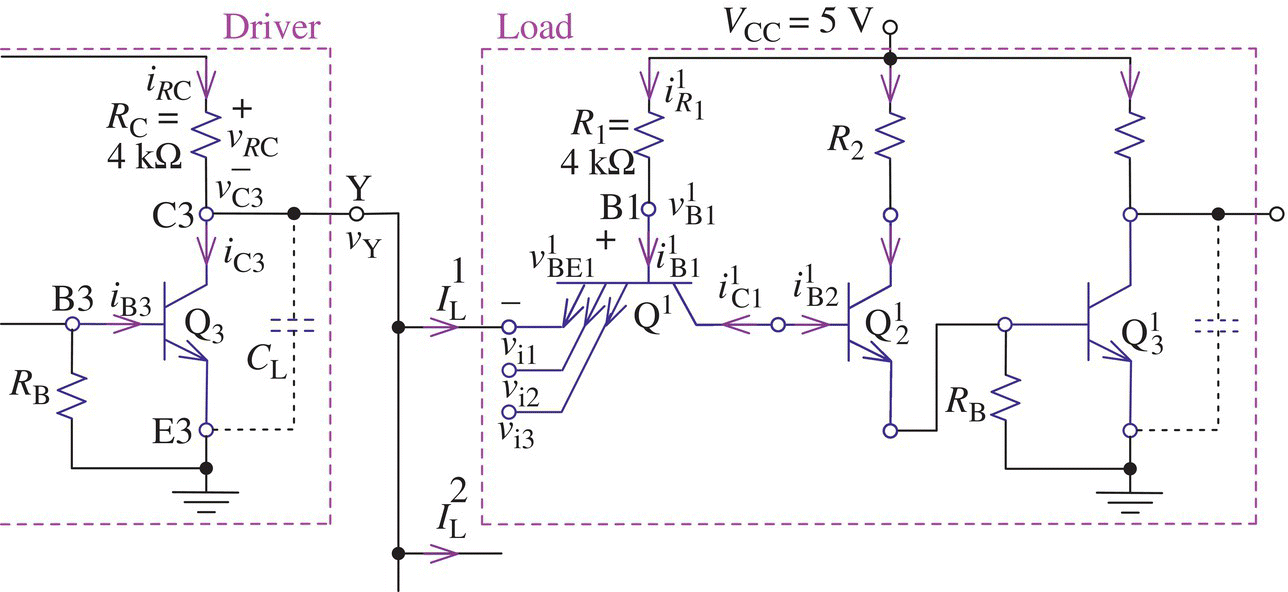
Figure 3.50 A TTL NAND gate as a driver with multiple loads.
If the number of load gates connected to the output node Y is N, the current through RC of the driver gate is
 , which will decrease the output voltage as(3.3.44)
In order for the output voltage vY not to be lower than the minimum output voltage 3 V (corresponding to logic 1) for all the voltage drop due to the loading effect, the following condition should be met:
Therefore the output‐high fan‐out of the TTL NAND gate of Figure 3.49 is 7.
- Output‐low Fan‐out
In Figure 3.50, suppose the output voltage of the driver gate is low, i.e. vY = VCE,sat = 0.2 V with the BJT Q saturated, which can drive the BJTs
 (connected to the output node Y),
  , and
, and  of the load gate (in the next stage) into the saturation, cutoff, and cutoff modes, respectively. Then the load current (flowing from the load gate) equal to the (negative) emitter current of
  can be obtained as(3.3.46)
If the number of load gates connected to the output node Y is N, the collector current iC3 of Q3 in the driver gate will be
(3.3.47)
In order for Q3 not to exit the saturation mode, the following condition should be met:
This implies that the output‐low fan‐out of the TTL NAND gate of Figure 3.49 is 54. Therefore, the fan‐out of the TTL NAND gate is 9, which is the lower of the output‐low and output‐high fan‐outs.
3.3.2.3 Totem‐Pole Output Stage
Consider again the TTL NAND gate of Figure 3.49 or 3.50 where CL denotes the capacitive load consisting of parasitic capacitances of wires and reverse‐biased diodes (of the load gates). The capacitive load CL may cause a long low‐to‐high transition time (as can be seen from Figure 3.27(b1)) since it must be charged from VCE,sat = 0.2 to VCC = 5.0 by the current ![]() through RC. A smaller RC reduces the output delay, but also results in a more power dissipation of (VCC −VCE,sat)2/RC when the output is low, i.e. vY = VCE,sat.
through RC. A smaller RC reduces the output delay, but also results in a more power dissipation of (VCC −VCE,sat)2/RC when the output is low, i.e. vY = VCE,sat.
To resolve this dilemma, the (passive) pull‐up resistor RC is made into an active pull‐up circuit by inserting a BJT Q4 (together with a diode D) between RC and Q3 as depicted in Figure 3.51. The circuit is called a TTL NAND gate with a totem‐pole output stage where totem poles are ancient traditional sculptures that were carved as the emblem of a family or clan by the Northwest American Indian tribes. Since its logic function is the same with the previous NAND gates, let us focus on the role of the totem‐pole output stage consisting of Q4‐D‐Q3, especially during the low‐to‐high transition of the output voltage vY.
First, let all the inputs of the gate be high. Then the BJTs Q1, Q2, and Q3 will be in the reverse‐active, saturation, and saturation modes, respectively, so that the output voltage can be
What difference does the additional BJT(Q4)‐diode(D) pair make in comparison with RC alone? It is expected to cut off the current iRC so that RC can dissipate no power during the low state of the output. Such an expectation comes true because the voltage difference between B4 and C3 (or Y)
is not high enough to turn on Q4‐D. (It would be not the case without D.)
Now, suppose that at least one of the inputs becomes low. Then the BJTs Q1, Q2, and Q3 operate in the saturation, cutoff, and cutoff modes, respectively, so that the voltage vB4 = vC2 can be pulled up high via R2 enough to turn on (saturate) Q4‐D where the output voltage (across CL) will remain at 0.2 V for the moment since the capacitor voltage cannot change instantaneously. Then CL will be charged by the emitter current of Q4 (saturated)
till iE4 becomes almost zero and accordingly, Q4 and D are just at the cut‐in condition with vBE4=VBE,offset=0.6 and vD=VD,offset=0.5 so that the output will reach
- (Q4) What is the role of the BJT Q4 placed atop Q3?
(A4)
- Static aspect: when the output voltage is high, Q4 can afford more load current with a smaller current through and voltage drop across R2 (with a much smaller output resistance) so that the output‐high fan‐out can be increased.
- Dynamic aspect: when the output changes from low (with Q3 saturated) to high (with Q3 cutoff), Q4 transfers from cutoff to saturation one jump ahead of the transfer of Q3 so that it can supply current to CL (charged to 0.2 V) as a source, reducing the low‐to‐high switching time.
- (Q5) What is the role of the diode D placed between the two BJTs Q3 and Q4?
- (A5) Without D, the voltage vB4 − vC3 = 0.8 V (Eq. (3.3.50)) will turn on Q4 alone when the output voltage is low as vY = vC3 = VCE3,sat = 0.2 V so that the collector current iC4 flowing through RC may result in a power dissipation.
- (Q6) What is the role of RC?
- (A6) With R2 = 0, the current determined by Eq. (3.3.51) would increase to reduce the low‐to‐high switch time. However, when Q4 turns on before Q3 turns off, the supply voltage VCC would be short‐circuited through C4‐E4‐D‐C3‐E3, possibly damaging Q4, D, and Q3. Therefore, RC is needed to limit such current spikes.
- (Q7) Is there any disadvantage of the totem‐pole output stage?
- (A7) Yes. The disadvantage is a lower output voltage (Eq. (3.3.52)) corresponding to logic 1.
- Output‐high Fan‐out
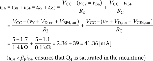
In Figure 3.51, suppose the output voltage of the driver gate is high, i.e. vY = 3.9 V with Q2/Q3/Q4 (in the current stage) cutoff/cutoff/saturated~cut‐in, which lets the load current of
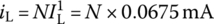 (Eq. (3.3.43)) flow into N load gates in the next stage. The BJT Q4 is supposed to use its emitter current iE4 = βFiB4 to supply this load current while the output voltage obtained by subtracting the voltage drops R2iR2 = R2iB4, VBE4,sat, and VD,on from VCC should be higher than the minimum output voltage 3 V (corresponding to logic 1):(3.3.53)
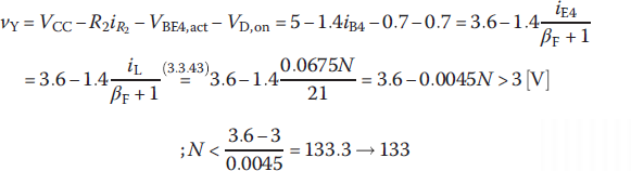
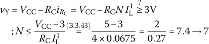
Therefore, the output‐high fan‐out of the TTL NAND gate with a totem‐pole output stage of Figure 3.51 is 133. Compare this with Eq. (3.3.45) for the NAND gate without the totem‐pole output stage.
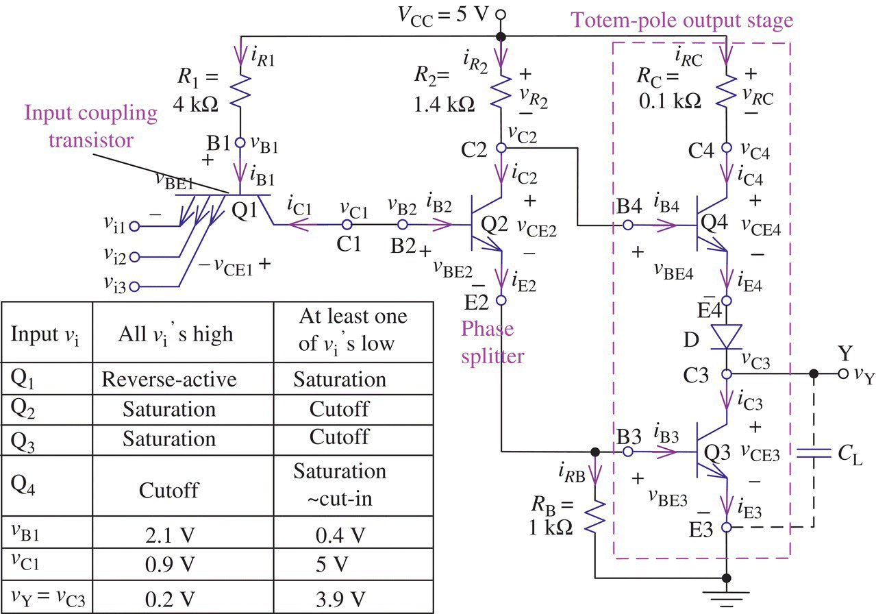
Figure 3.51 A TTL NAND gate with a totem‐pole output stage.
- Output‐low Fan‐out
In Figure 3.51, suppose the output voltage of the driver gate is low, i.e. vY = VCE,sat = 0.2 V with Q2/Q3/Q4 (in the current stage) saturated/saturated/cutoff. In order for the saturation mode of Q3 not to be disturbed by the load current (flowing from the load gate), the condition described by Eq. with iRC = 0 should be satisfied:
(3.3.54)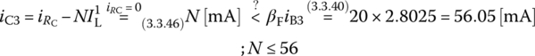
Compare this with Eq. (3.3.48) for the NAND gate without the totem‐pole output stage.
- PSpice Simulation of the TTL NAND Gate with a Totem‐Pole Output Stage
Figure 3.52(a)/(b) shows the PSpice schematic and its simulation result (for Transient Analysis with maximum stepsize 1 ns) of the TTL NAND gate with a totem‐pole output stage depicted in Figure 3.51. Here are several observations about the simulation result (Figure 3.52(b)) where one of the two input voltages is fixed as 4 V(HIGH) and the other v1(t) is a rectangular pulse plotted as a green line:
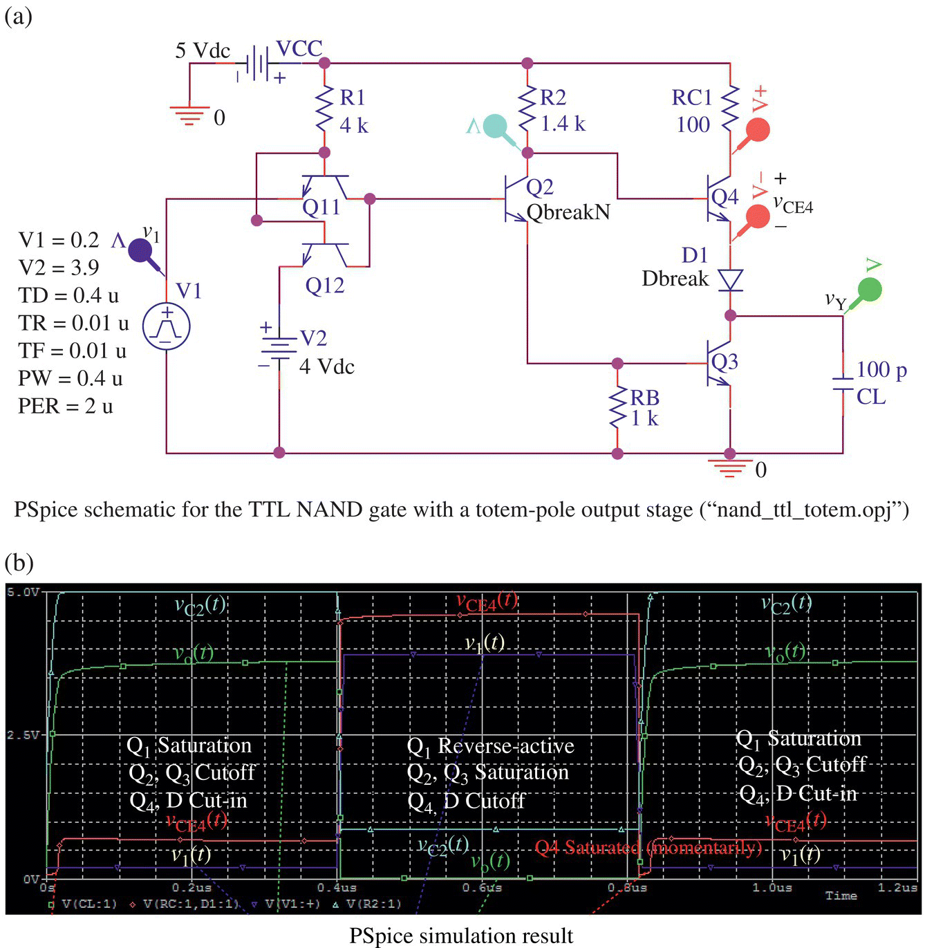
Figure 3.52 PSpice simulation of the TTL NAND gate with a totem‐pole output stage depicted in Figure 3.51
- When the input v1(t) is LOW/HIGH, the output vY(t) is HIGH/LOW. This implies that the circuit works fine as a NAND gate.
- When at least one of the inputs, say, v1(t) plotted as a blue line is LOW (0.2 V), Q1/Q2/Q3/Q4/D are in the saturation/cutoff/cutoff/cut‐in/cut‐in modes, respectively, but Q4 and D momentarily enter the saturation mode with vCE4 ≤ 0.2 V and vD ≥ 0.75 V, respectively, (before cut‐in) to charge CL during the LOW‐to‐HIGH transition time of vY(t). After transients, Q4 and D are in the cut‐in mode where vCE4 = 0.66 V, vBE4 = 0.66 V, vD = 0.55 V, and iD = 15 μA.
- When all the inputs are HIGH (3.9 V), Q1/Q2/Q3/Q4/D are in the reverse‐active/saturation/saturation/cutoff/cutoff modes, respectively, where vBC1 = 0.75 V, vBE2 = 0.82 V, vCE2 = 0.038 V, vBE3 = 0.82 V, vCE3 = 0.018 V, vBE4 ≤ 0.5 V, vCE4 = 4.6 V, and vD ≤ 0.4 V.
- The high output voltage is 3.8 V, being close to 3.9 V predicted by Eq. (3.3.52), but the low output voltage is 0.018 V, being lower than VCE3,sat = 0.2 V (predicted by Eq. (3.3.49)).
3.3.2.4 Open‐Collector Output and Tristate Output
The output impedance of the TTL NAND gate (with totem‐pole output stage) is very low irrespective of whether its output is HIGH or LOW. In most cases, the low output impedance is desired because it contributes towards improving the fan‐out capability by reducing the loading effect. However, in the case of bus contention where different gates attempt to drive a wired‐OR output (as depicted in Figure 3.53(a)) into different logic states, the low output impedance is not good because it may cause an excessive current to flow from HIGH‐output gates to LOW‐output gates. Against such a happening, open‐collector outputs (as depicted in Figure 3.53(b)) can be used where each one of the gates with an open‐collector output drives the wired‐OR output LOW if it wants a LOW output; otherwise it lets its output float (leaving up to other gates’ decision) so that the wired‐OR output can be pulled up HIGH (via an external pull‐up resistor connected to VCC) only when no gate pulls down the output by asserting LOW.
Another measure against bus contention is to use the tristate output illustrated in Figure 3.53(c) where if the (low‐active) Disable input ![]() is 0.2 V (LOW), the BJTs Q1, Q2, and Q3 are in the saturation, cutoff, and cutoff modes, respectively, and the diode D is ON so that vB4=vDis+vD,ON=0.2+0.7=0.9[V]. This voltage will turn on just Q4‐R4 so that vB5=vB4−0.7=0.2[V]. This voltage is not sufficient to turn on Q5. Thus, both Q3 and Q5 are OFF so that the gate can let its output float with a very high output resistance when
is 0.2 V (LOW), the BJTs Q1, Q2, and Q3 are in the saturation, cutoff, and cutoff modes, respectively, and the diode D is ON so that vB4=vDis+vD,ON=0.2+0.7=0.9[V]. This voltage will turn on just Q4‐R4 so that vB5=vB4−0.7=0.2[V]. This voltage is not sufficient to turn on Q5. Thus, both Q3 and Q5 are OFF so that the gate can let its output float with a very high output resistance when ![]() is low. Otherwise, i.e. if
is low. Otherwise, i.e. if ![]() is high, the gate performs a usual NAND function. This gate is said to have a tristate or three‐state output because it presents three outputs, i.e. HIGH, LOW, and FLOAT (high impedance) states. The
is high, the gate performs a usual NAND function. This gate is said to have a tristate or three‐state output because it presents three outputs, i.e. HIGH, LOW, and FLOAT (high impedance) states. The ![]() input is used to select only one gate among the gates that are wired‐OR connected. Note that the tristate outputs must be pulled up or down to keep the output from being floated, i.e. indeterminate or in the high impedance (Hi‐Z) state when all the drivers are disabled.
input is used to select only one gate among the gates that are wired‐OR connected. Note that the tristate outputs must be pulled up or down to keep the output from being floated, i.e. indeterminate or in the high impedance (Hi‐Z) state when all the drivers are disabled.
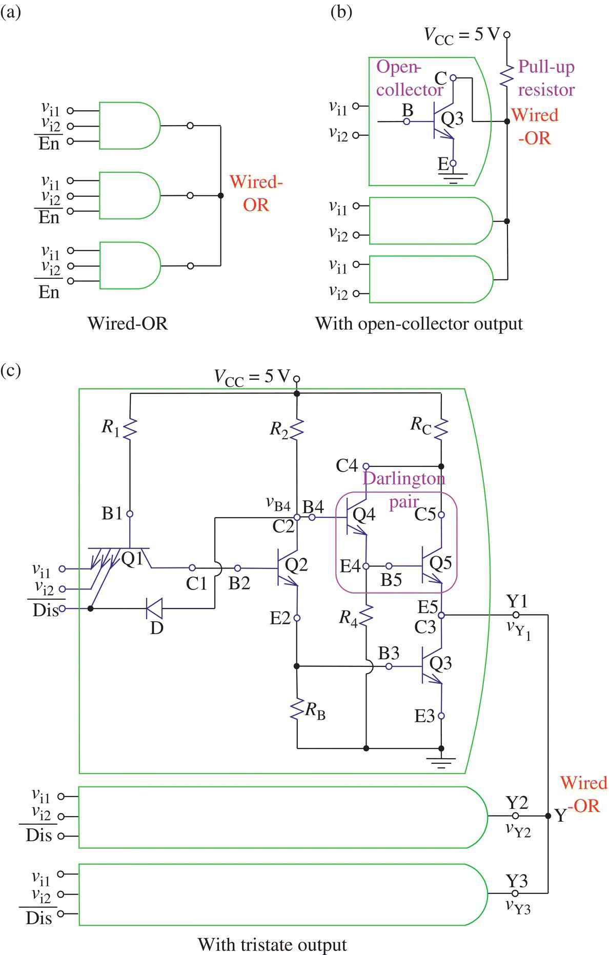
Figure 3.53 Tristate output and open‐collector output for wired‐OR connection
3.3.3 ECL (Emitter‐Coupled Logic) OR/NOR Gate
Figure 3.54 shows an ECL (Emitter‐Coupled Logic) OR/NOR gate, which consists of a differential amplifier using emitter‐coupled pair (Section 3.1.11), a reference voltage supplier, and a level shifter. Compared with the TTL family, the ECL family achieves very fast switching and short propagation delays by keeping the BJTs in the forward‐active mode (away from the saturation mode) so that there can be no excessive stored charge to remove quickly. However, it exhibits more power consumption, reduced noise margin, smaller voltage swing, and higher fan‐out capability.
Here is a rough analysis of the ECL circuit in Figure 3.54, which is designed to have all the BJTs operate in the forward‐active mode although the two input BJTs Q1 and Q2 may be saturated when the corresponding input voltage vi1/vi2 is much higher than Vref = 2.25 [V] supplied to the base B3 of Q3. The reference voltage supplier consisting of RC4‐Q4‐R4‐Q8‐R8 supplies the nodes B3 and B7 with
Figure 3.54 An ECL (Emitter‐Coupled Logic) OR/NOR gate.

The BJT Q7, given vB7 = 1.15 [V] at its base terminal B7, produces its emitter current
so that Q7 makes the current iC7 = αFiRE/(1 + αF) ≈ 1.75 [mA] through Q1|Q2|Q3‐Q7‐RE like a current source of 1.75 [mA]. This current iC7 ≈ 1.75 [mA] will flow through RC (with Q1 and/or Q2 in the forward‐active mode and Q3 in the cutoff mode) if any one of the two inputs vi1 and vi2 is higher than vB4 = 2.25[V]= Vref; otherwise, i.e. none of the inputs is higher than vB4 = 2.25[V] = Vref, the current iC7 ≈ 1.75 [mA] will flow through RC3 (with Q1 and Q2 in the cutoff mode and Q3 in the forward‐active mode). In the former case, the emitter voltages of Q5 and Q6 will be
In the latter case, the emitter voltages of Q5 and Q6 will be
As an exception, when the input voltage vi1/vi2 is much higher than Vref = 2.25[V] (supplied to the base B3 of Q3), the corresponding BJT Q1|Q2 will be saturated with vCE ≤ 0.2[V] so that vNOR will rise with the input voltage vi:
This rough analysis results are supported by the VTC that is obtained from the PSpice simulation (with DC Sweep analysis type) and depicted in Figure 3.55(b1). Note that the input voltages vi1/vi2 applied to the ECL gates should never be much higher than Vref = 2.25 [V] to keep the BJTs Q1|Q2 from being saturated.
- (Q8) What is the role of R1/R2 each connected in parallel with the input vi1/vi2?
- (A8) It provides a matching termination impedance for a 50Ω‐transmission line feeding the input. It will also pull down an input terminal which is connected to no gate so that indeterminate logic levels and noise can be prevented.
Figure 3.55 PSpice simulation of an ECL OR/NOR gate (“or_ecl3.opj”).
- (Q9) Why is the VTC for vOR=vC3 − 0.75 symmetric while that for vNOR = vC2 − 0.75 is asymmetric?
- (A9) Because Q3 involved in producing vC3 is driven by the fixed reference voltage Vref = 2.25[V], while Q1|Q2 involved in producing vC2 are driven by the varying input voltage vi, which may saturate the corresponding BJT Q1|Q2 if it becomes much higher than Vref = 2.25[V] (supplied to the base B3 of Q3).
- (Q10) Why is RC = 587 Ω (connected with Q1|Q2) slightly smaller than RC3 = 600 Ω (connected with Q3)?
- (A10) RC has been made slightly smaller than RC3 to have RCiE,2 (with vi > Vref → Q1|Q2 ON and Q3 OFF → vNOR = VCC − RCiE,2 − vBE6) close to RC3iE,3 (with vi<Vref → Q1|Q2 OFF and Q3 ON → vOR = VCC −RC3iE,3 − vBE5) where iE2 of Q1|Q2 driven by vi > Vref is slightly larger than iE3 of Q3 driven by Vref.
Figure 3.55(b2) shows the power dissipations of each part that are obtained by attaching the Power Markers (Probes) to the parts or using the Trace>Add_Trace menu. For example, to see the sum of the powers dissipated by the reference voltage supplier (consisting of RC4‐Q4‐R4‐Q3‐RC4), you should type the following expression into the Trace Expression field in the lower part of the Add Traces dialog box opened by selecting the Trace>Add Trace menu in the PSpice A/D (Probe) Window (see Appendix D.2.8):
W(RC4)+W(Q4)+W(R4)+W(Q8)+W(R8) |
The power curve of Q1|Q2 plotted in gray tells us that Q1|Q2 will dissipate less power if they transit from the forward‐active mode into the saturation mode as the corresponding input voltages applied to their base terminals become much higher than Vref = 2.25[V].
3.4 Design of BJT Amplifier
This section will show how a CE amplifier (Figure 3.30(a)) with a desired voltage gain Av,d or CC amplifier (Figure 3.32(a)) with a desired input resistance Ri,d can be designed, i.e. how the values of resistors constituting the circuits can be determined to satisfy the design specification.
3.4.1 Design of CE Amplifier with Specified Voltage Gain
To maximize the AC swing of output voltage vo along the AC load line (see Figure 3.56.2) of CE amplifier (Figure 3.56.1(a)), it may be good to set the collector current IC,Q and collector‐to‐emitter voltage VCE,Q of BJT at the operating point Q as half the maximum collector current and about one third of VCC, respectively, and also to determine such a value of RC that the iC intercept of the AC load line can be about 2IC,Q:
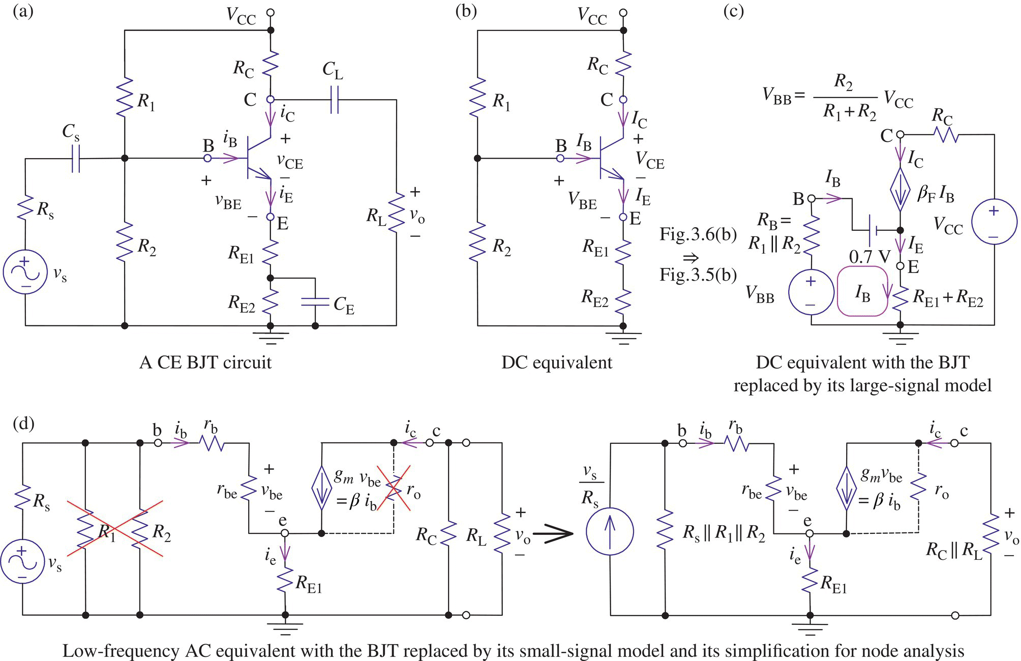
Figure 3.56.1 A CE (common‐emitter) amplifier and its DC/AC equivalents (see Figure 3.19.1).
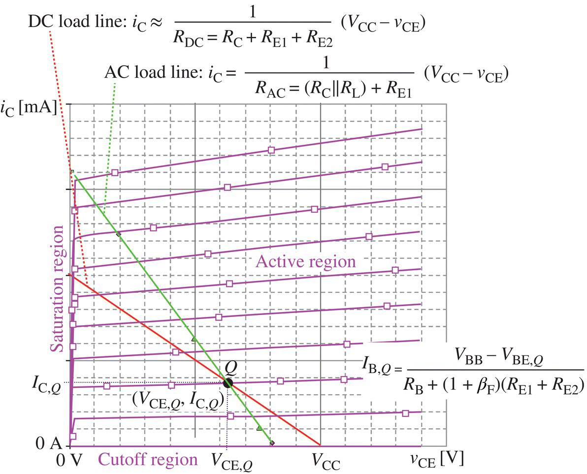
Figure 3.56.2 DC and AC load lines for the CE (common‐emitter) amplifier in Figure 3.56.1(a) (see Figure 3.22).
Here, RE1, which is a part of the AC resistance ![]() , has been neglected because it is presumably much less than (RC||RL) as well as has not yet been determined.
, has been neglected because it is presumably much less than (RC||RL) as well as has not yet been determined.
Then, in the DC equivalent circuit, the emitter and collector resistors are supposed to share the voltage drop VCC−VCE,Q = (1−KC)VCC:
where
Now, to determine the resistances R1 and R2 of DC biasing circuit (Figure 3.56.1(b)), we let the equivalent base resistance RB=R1||R2 be 1/10 times the equivalent emitter resistance (βF+1)RE:
Then, the equivalent base voltage source VBB and the biasing resistances R1 and R2 are determined as follows:
Now, with the transconductance gm and base‐emitter resistance rbe

Eq. (3.2.3) is used to determine the dual emitter resistance [RE1, RE2] so that the desired voltage gain Av,d can be achieved:
Note that the minimum power ratings of R1, R2, RC, RE1, and RE2 should be
This procedure of designing a CE amplifier with a specified voltage gain Av,d gain has been cast into the following MATLAB function ‘BJT_CE_design()’ where the default values of design constant Kc and ambient temperature T are set to 1/3 and 27 [oC], respectively.
To use the function for designing a CE BJT (Q2N2222) amplifier with voltage gain Av,d = ‐20, we run the above MATLAB script “design_CE_BJT.m,” which yields
>>design_CE_BJTDesign ResultsR1 R2 RC RE1 RE2 Avd13945 9147 309 14 277 20Results of analysis using the PWL modelVCC VEE VBB VBQ VEQ VCQ IBQ IEQ ICQ18.00 0.00 7.13 6.55 5.85 11.81 1.06e-04 2.01e-02 2.00e-02gm= 773.667[mS], rbe= 244[Ohm], ro= 5.00[kOhm]Gv=Ri/(Rs+Ri)xAv= 0.974 x -19.88 = -19.37
These results mean the following values of the resistances of designed CE amplifier:
where the BJT parameters, the source/load resistances, and VCC are given as
The results of using ‘BJT_CE_analysis()’ (see Section 3.2.1) to analyze the designed circuit are
with the expected voltage gain −19.37, transconductance gm = 0.774, and BEJ resistance rbe = 244 Ω.
Figure 3.57(a) and (b) shows the PSpice schematic of the designed CE amplifier and its simulation results. Although the resulting voltage gain Av,PSpice = −3.7172/0.2 = −18.6 is somewhat smaller than Av,d = −20 required by the design specification, the difference is not so big as to damage the reliability of the MATLAB design and analysis functions.
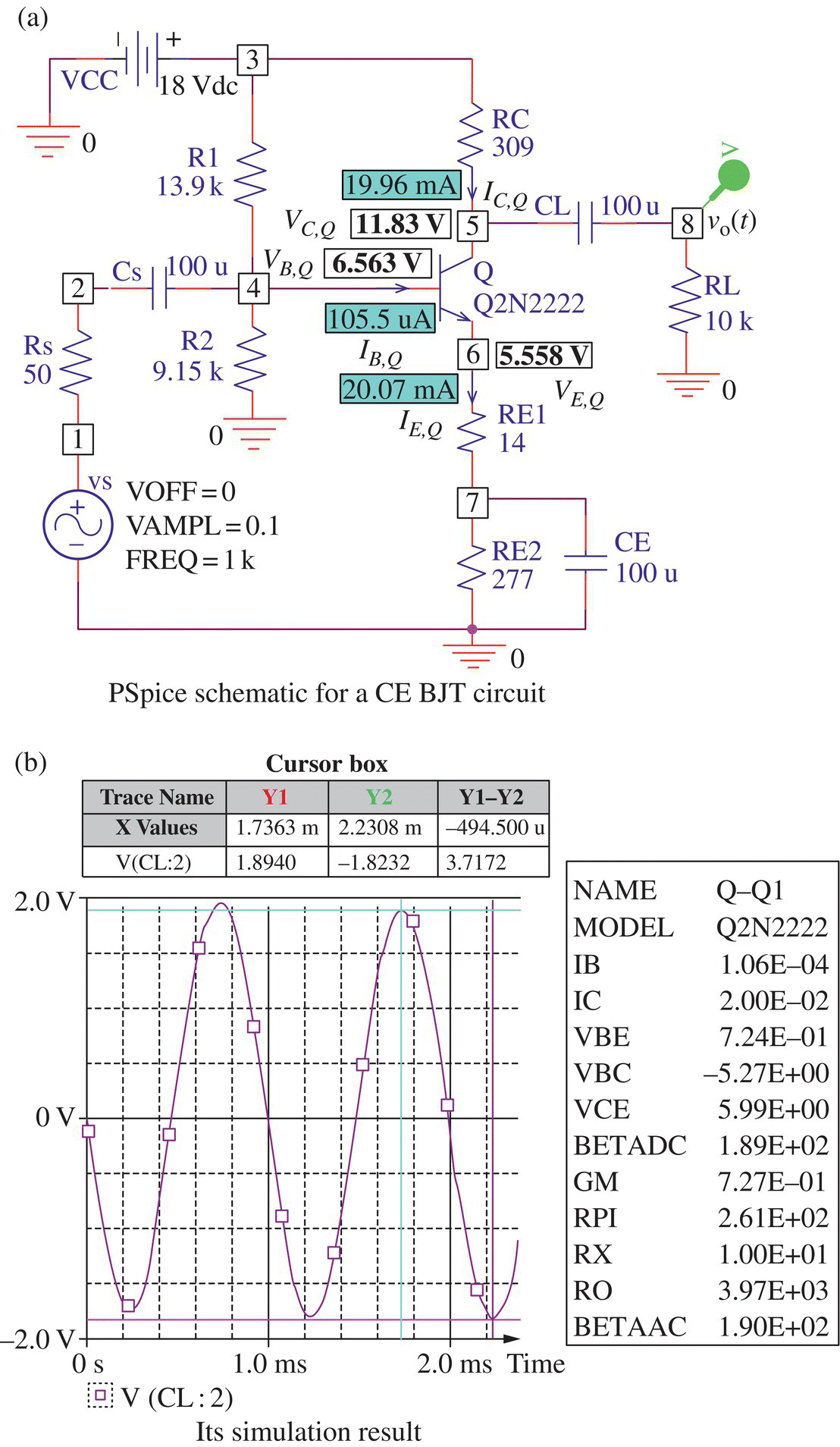
Figure 3.57 A CE circuit and its PSpice simulation (“elec03f53.opj”).
3.4.2 Design of CC Amplifier (Emitter Follower) with Specified Input Resistance
Let us consider how to determine the values of resistors constituting the CC amplifier (Figure 3.58(a)) such that the input resistance (Eq. (3.2.5)) has a given value Ri,d.
To maximize the AC swing of output voltage vo, it may be good to let the C‐E junction and RE share the applied voltage VCC half and half (at the operating point Q) in the DC equivalent circuit (Figure 3.58(b) or (c)) so that
KVL around the VBB‐RB‐0.7 V‐VE loop yields
From Eqs. (3.4.15b) and (3.4.16), we can have the expressions of RE and RB in terms of IC,Q as
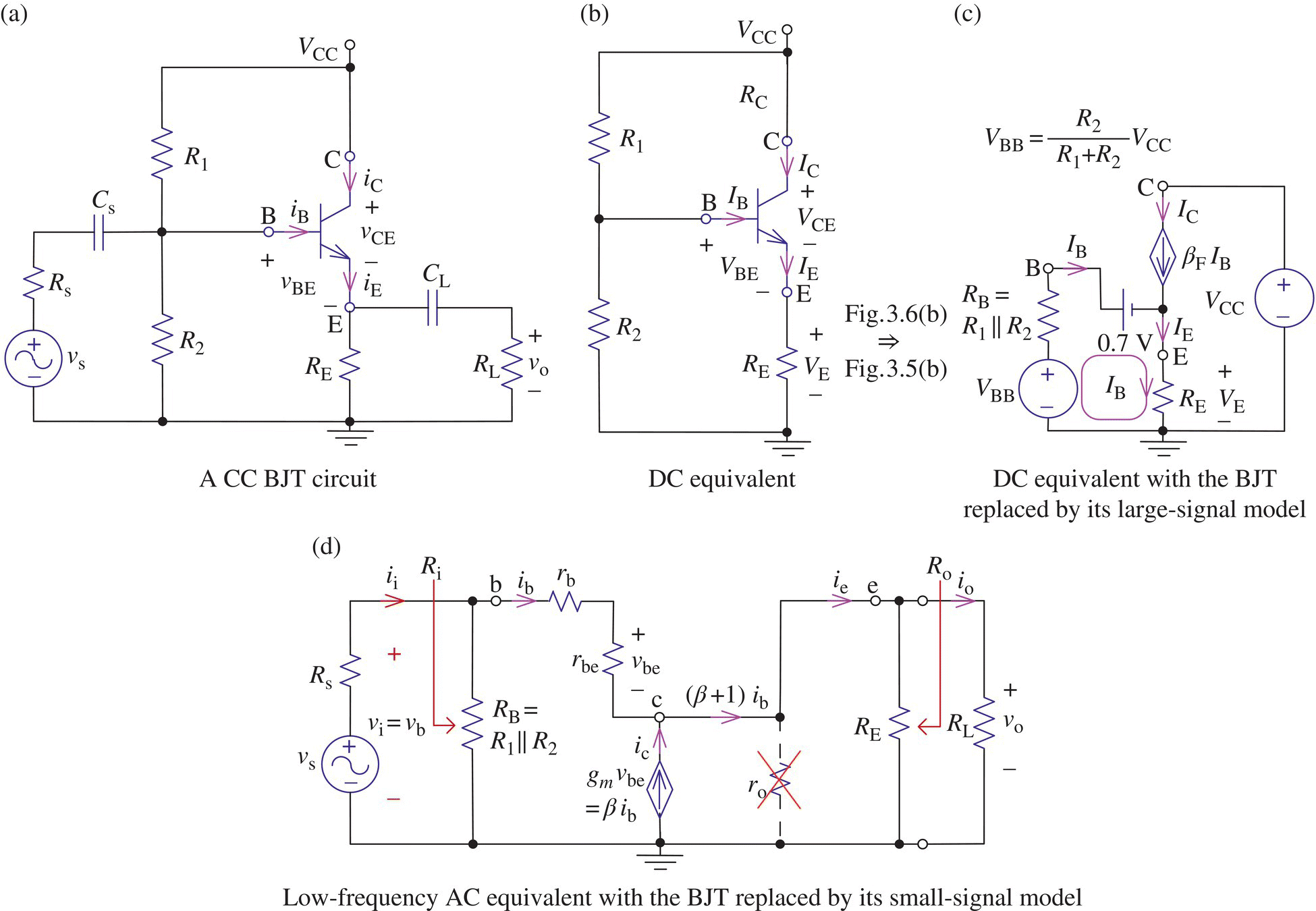
Figure 3.58 A CC (common‐collector) or emitter follower circuit and its DC/AC equivalents (see Figure 3.19.1).
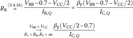
where R2 has been assumed to be open‐circuited to maximize the range of RB. Then it is key to choose IC,Q from the range (IC,max/100, IC,max/2) such that Eq. (3.4.14) with Eqs. (3.4.17a,b) can be satisfied. Once such a value of IC,Q is determined, the resistances RE, R1=RB, the resulting input resistance Ri, and the output resistance Ro can be computed using Eqs. where Eqs. (3.4.14) (or Eq. (3.2.5)) and (3.2.8) have been coded in the MATLAB function ‘BJT_CC_analysis()’. However, if IC,Q turns out to be small enough to endanger the swing of AC collector current, i.e.
then another BJT with larger current gain βF should be used. This procedure of designing a CC amplifier with a specified input resistance Ri,d has been cast into the above MATLAB function ‘BJT_CC_design()’ where the default values of IC,max and ambient temperature T are set to 0.8 and 27[°C], respectively.
To use the function for designing a CC BJT (Q2N2222) amplifier with input resistance, Ri,d = 50 kΩ, we run the above MATLAB script “design_CC_BJT.m,” which yields
>>design_CC_BJTDesign ResultsR1 RE Rid ICQ98810 536 50000 0.01680Analysis ResultsVCC VBQ VEQ VCQ IBQ IEQ ICQ18.00 9.72 9.02 18.00 8.38e-005 1.68e-002 1.68e-002in the forward-active mode with VCE,Q= 8.98Ri= 47.175[kOhm], Ro= 2[Ohm]Gv=Ri/(Rs+Ri)xAv = 0.999 x 1.00 = 1.00
These results mean the following values of the resistances of the designed CC amplifier:
where the BJT parameters, the source/load resistances, and VCC are given as
The results of using ‘BJT_CC_analysis()’ (see Section 3.2.2) to analyze the designed circuit are
'Is the input resistance Ri = 47.175 kΩ of designed CC amplifier close to Ri,d = 50 kΩ?
Figure 3.59(a) and (b) shows the PSpice schematics and their simulation results for measuring the input/output resistances of the designed circuit. The PSpice measured input resistance Ri,PSpice = Vs/Is − Rs = 0.1 V/1.984 μA − 50 Ω = 50.35 kΩ is very close to Ri,d = 50 kΩ required by the design specification. The PSpice measured output resistance Ro,PSpice = 0.1 V/62.793 mA = 1.59 Ω is close to Ro = 1.8 Ω predicted by the MATLAB analysis result.
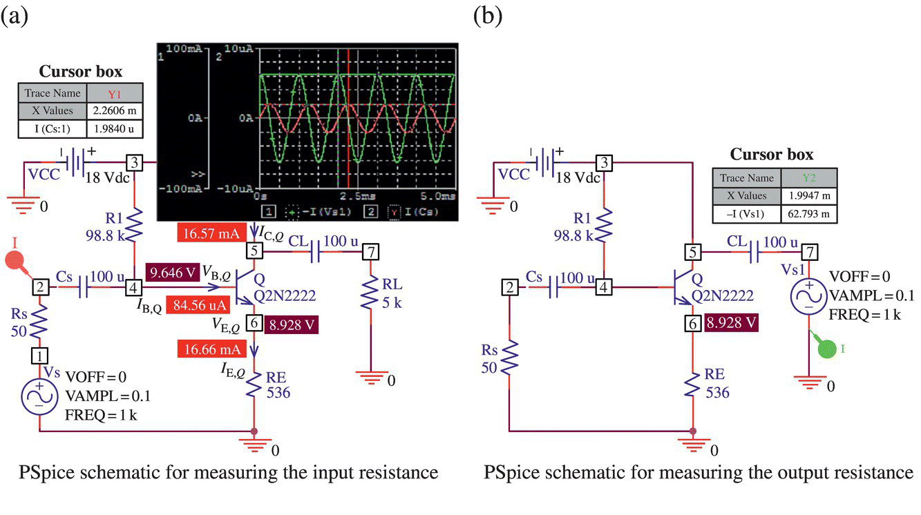
Figure 3.59 A CC circuit and its PSpice simulation (“elec03f55.opj”).
3.5 BJT Amplifier Frequency Response
In this section, we will find the transfer function G(s) = Vo(s)/Vi(s) and frequency response G(jω) for a CE amplifier, a CC amplifier, and a CB amplifier with the BJT replaced by the high‐frequency small‐signal model shown in Figure 3.18(a).
3.5.1 CE Amplifier
Figure 3.60(a) and (b) shows a CE amplifier circuit and its high‐frequency small‐signal equivalent, respectively, where one more load capacitor CLL, in addition to the output capacitor CL, is connected in parallel with the load resistor RL. For the equivalent circuit shown in Figure 3.60(b), a set of three node equations in V1, V2 = Vc, and V3 = Ve can be set up as
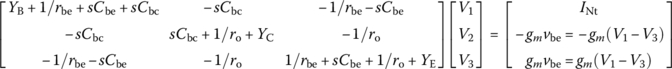
where
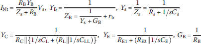
- (Q) How about if RE1 = 0?
Here, INt and YB are the values of Norton current source and admittance looking back into the source part from terminals 1 to 0 as shown in Figure 3.60(c1) and (c2). This equation can be rearranged into a solvable form with all the unknown terms on the LHS as
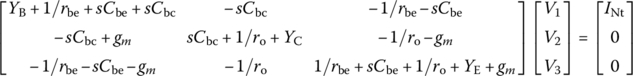
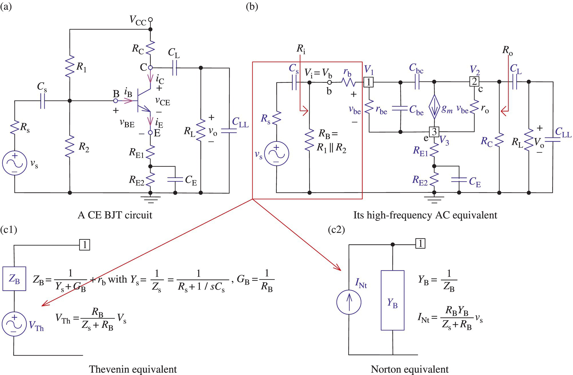
Figure 3.60 A CE (common‐emitter) BJT circuit and its high‐frequency AC equivalent.
and solved for V1, V2, and V3. Then the transfer function and frequency response can be found as

This process to find the transfer function and frequency response has been cast into the following MATLAB function ‘BJT_CE_xfer_ftn()’.
Note the following about the internal capacitances of a BJT, the base‐to‐emitter capacitance Cbe, the base‐to‐collector capacitance Cbc, and the collector‐to‐emitter capacitance Cce [W-7]:
- Cce can usually be ignored since Cce ≪ Cbe.
- Cbe and Cbc can be modeled as voltage‐dependent capacitors with values determined by
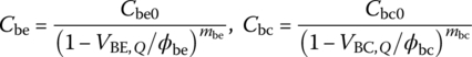
- where Cbe0(CJE)/Cbc0(CJC): zero‐bias B‐E/B‐C junction capacitances, VBE,Q/VBC,Q: quiescent B‐E/B‐C voltages[V], mbe(MJE)/mbc(MJC): B‐E/B‐C grading coefficient, and ϕbe(VJE)/ϕbc(VJC): B‐E/B‐C built‐in potential[V].
Referring to Figure 3.61, four break (pole or corner) frequencies determining roughly the frequency response magnitude can be determined as [R-2]
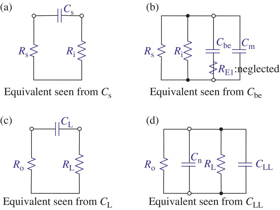
Figure 3.61 (Approximate) equivalent circuits for finding the equivalent resistance seen from each capacitor.
Note the following about these four break frequencies:
- ωC1, related with the coupling capacitor Cs, is obtained as the reciprocal of the product of Cs and the equivalent resistance as seen from Cs (see Figure 3.61(a)).
- ωC2, related with the output capacitor CL, is obtained as the reciprocal of the product of CL and the equivalent resistance as seen from CL (see Figure 3.61(c)).
- ωC3, related with the internal capacitors Cbe|Cbc, is obtained as the reciprocal of the product of (Cbe+Cm) and the equivalent resistance as seen from Cbe (see Figure 3.61(b)).
- ωC4, related with the internal capacitors Cbc|CLL, is obtained as the reciprocal of the product of (Cn+CLL) and the equivalent resistance as seen from CLL (see Figure 3.61(d)).
- The passband of the CE amplifier will be approximately lower‐/upper‐bounded by the second/third highest break frequencies where not only the values but also the order of the frequencies varies with the values of the related capacitances and resistances.
Note also that Ri/Ro are the input/output resistances of the CE amplifier, respectively, and Cm/Cn are the Miller equivalent capacitances for capacitor Cbc seen from the input/output sides, respectively (see Eq. (1.4.2)):
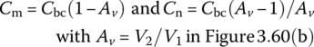
The following MATLAB function ‘break_freqs_of_CE()’ uses Eqs. (3.5.6a,b) to find the four break frequencies:
3.5.2 CC Amplifier (Emitter Follower)
Figure 3.63(a) and (b) shows a CC amplifier circuit and its high‐frequency small‐signal equivalent, respectively, where one more load capacitor CLL, in addition to the output capacitor CL, is connected in parallel with the load resistor RL. For the equivalent circuit shown in Figure 3.63(b), a set of three node equations in V1, V2 = Ve, and V3 = Vc can be set up as

Figure 3.62 A CE amplifier circuit and its frequency response from PSpice and MATLAB (“elec03e18.opj”).
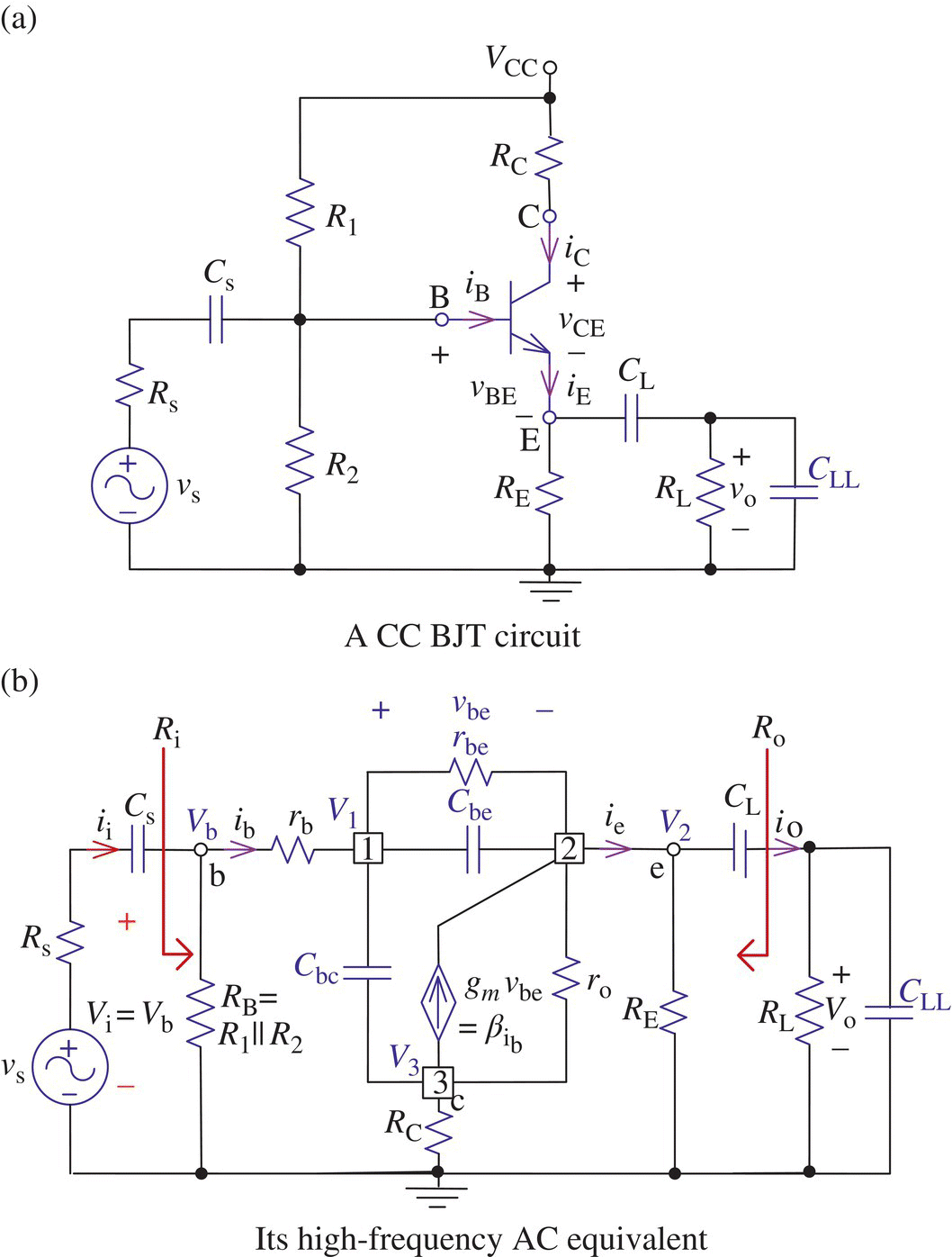
Figure 3.63 A CC (common‐collector) BJT circuit and its high‐frequency AC equivalent.
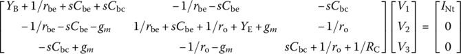
where

- (Q) How about if RC = 0?
Solving this set of equations, we can find the transfer function and frequency response as

This process to find the transfer function and frequency response has been cast into the above MATLAB function ‘BJT_CC_xfer_ftn()’.
There are four break (pole or corner) frequencies determining roughly the frequency response magnitude:
where Ri/Ro are the input/output resistances of the CC amplifier, respectively, and Cm/Cn are the Miller equivalent capacitances for capacitor Cbe seen from the input/output side, respectively (see Eq. (1.4.2)):
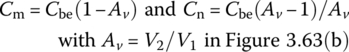
Note that Eq. (3.5.11) is just like Eq. (3.5.6) with Cbc and Cbe switched.
The following MATLAB function ‘break_freqs_of_CC()’ uses Eqs. (3.5.11a,b) to find the four break frequencies:
3.5.3 CB Amplifier
Figure 3.65(a) and (b) shows a CB amplifier circuit and its high‐frequency small‐signal equivalent, respectively, where one more load capacitor CLL, in addition to the output capacitor CL, is connected in parallel with the load resistor RL. Note that if the terminal B(ase) is not AC grounded via a capacitor CB, we should let CB = 0 in Figure 3.65(b). For the equivalent circuit shown in Figure 3.65(b), a set of three node equations in V1 = Ve, V2 = Vc, and V3 = Vb can be set up as
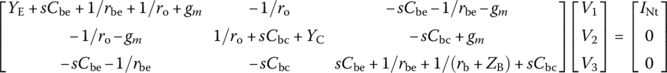

Figure 3.64 A CC amplifier circuit and its frequency response from PSpice and MATLAB (“elec03e19.opj”).
where
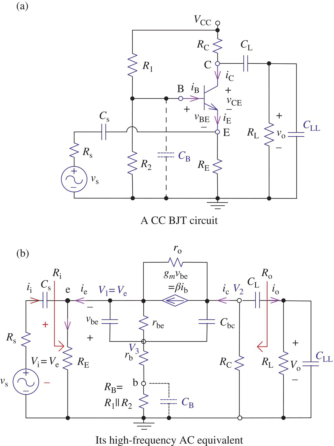
Figure 3.65 A CB (common‐base) BJT circuit and its high‐frequency AC equivalent.
- (Q) How about if rb = 0 and RB = 0 or CB is so large that RB can be regarded as AC‐shorted?
Solving this set of equations, we can find the transfer function and frequency response as

This process to find the transfer function and frequency response has been cast into the above MATLAB function ‘BJT_CB_xfer_ftn()’.
There are four break (pole or corner) frequencies determining roughly the frequency response magnitude:
where Ri/Ro are the input/output resistances of the CB amplifier, respectively, and
The following MATLAB function ‘break_freqs_of_CB()’ uses Eqs. (3.5.16a,b) to find the four break frequencies:
3.6 BJT Inverter Time Response
In this section, let us see the time response of a basic BJT inverter (as shown in Figure 3.27(a1) or 3.67(b)) to logic low‐to‐high and high‐to‐low input transitions. About Figure 3.27(b1) illustrating the low‐to‐high and high‐to‐low propagation delays, one might wonder what makes the circuit seemingly not having any dynamic elements such as capacitors or inductors exhibit a dynamic time response to the piece wisely constant input. It stems from internal parasitic capacitances between the terminals of the BJT, whose effect becomes conspicuous as the frequency or slope of the input increases, while negligible for a DC or low‐frequency input.
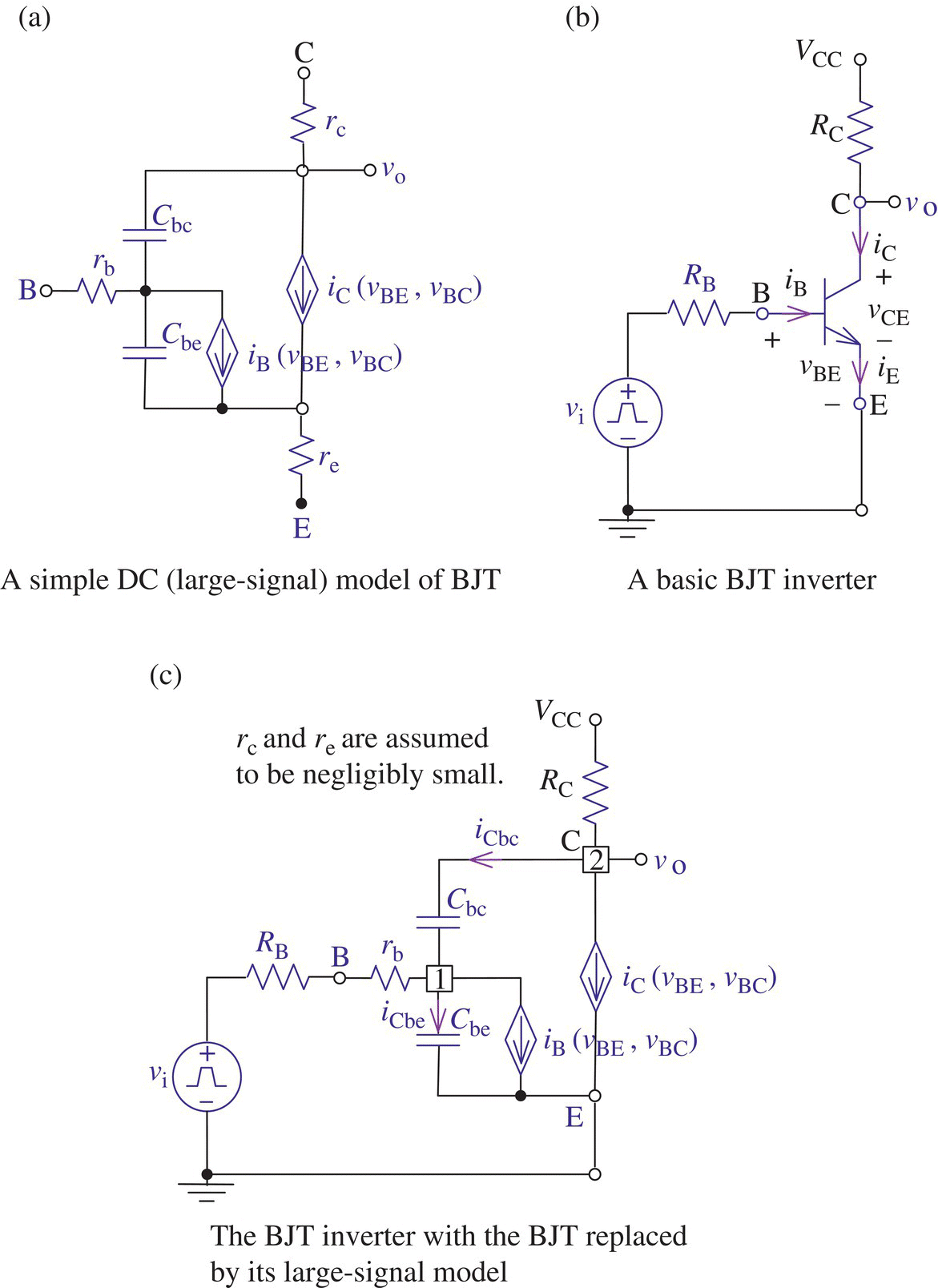
Figure 3.67 A simple large‐signal Spice model of BJT and the equivalent of a BJT inverter adopting the model.
Figure 3.67(a) shows a simple DC or large‐signal Spice model of a BJT where iC(vBE,vBC) and iB(vBE,vBC) are defined as Eqs. (3.1.23a,b), respectively, and
- rb: base resistance, re: emitter resistance, rc: collector resistance,
- Cbc: base‐collector junction capacitance, and
- Cbe: base‐emitter junction capacitance.
Figure 3.67(c) shows a DC equivalent of the inverter (Figure 3.67(b)) with the BJT replaced by its large‐signal model (Figure 3.67(a)). To solve the circuit in a numerical way, we should know the following:
- From the KCL equations at nodes 1 and 2, the currents iCbc and iCbe, each through Cbc and Cbe, respectively, can be expressed as
where
- These currents charge each one of the capacitors, Cbc and Cbe, respectively, as
A process of solving the inverter to find the output vo(t) to an input vi(t) (based on these equations) has been cast into the above MATLAB function ‘BJT_inverter_dynamic()’. Note the following about the dynamic behavior of the inverter:
- The collector resistor RC and the (internal) base‐collector capacitance Cbc affect how long it takes for Cbc to be charged up to VCC, via the time constant during the rising period of vo(t).
- The base resistor RB and the (internal) base‐emitter capacitance Cbe affect how long it takes for Cbe to be charged up to VBE = 0.7 V, via the delay time during the falling period of vo(t).
Note that the time constant of an RC circuit, i.e. the time taken for its transient response to reach 63.2% of its final value, is RC where R/C is the equivalent resistance/capacitance seen from C/R.
Problems
- 3.1 Circuit with an NPN‐BJT Forward Biased
Consider the BJT biasing circuit in Figure P3.1.1(a) where the device parameters of the BJT Q1 are βF = 154, βR = 6.092, and Is(saturation current) = 14.34−15 A.
- Referring to Figure P3.1.1(b), find iC and vCE of the circuit with RC = 1 kΩ, RE = 1 kΩ, and VCC = 5 V by hand. Then do the same thing two times, once (based on the piecewise linear [PWL] model) by using
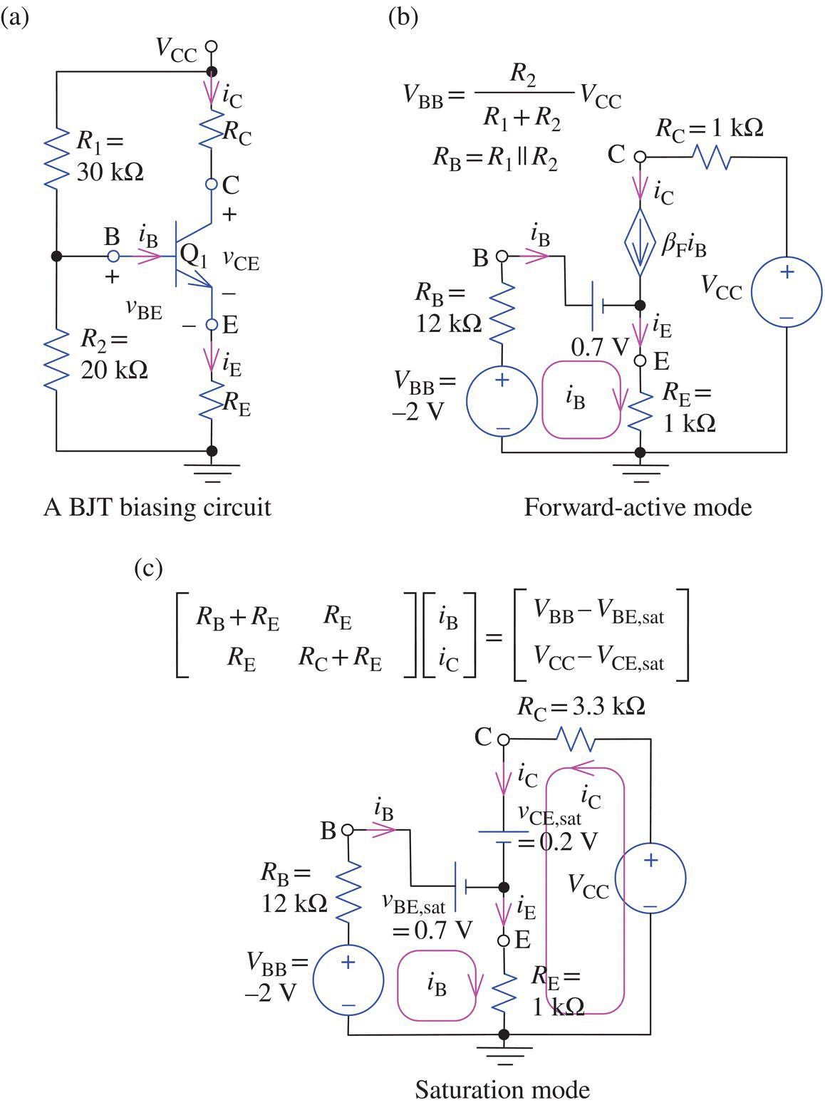
Figure P3.1.1 A BJT biasing circuit and its equivalents in different operation modes (regions) of BJT.
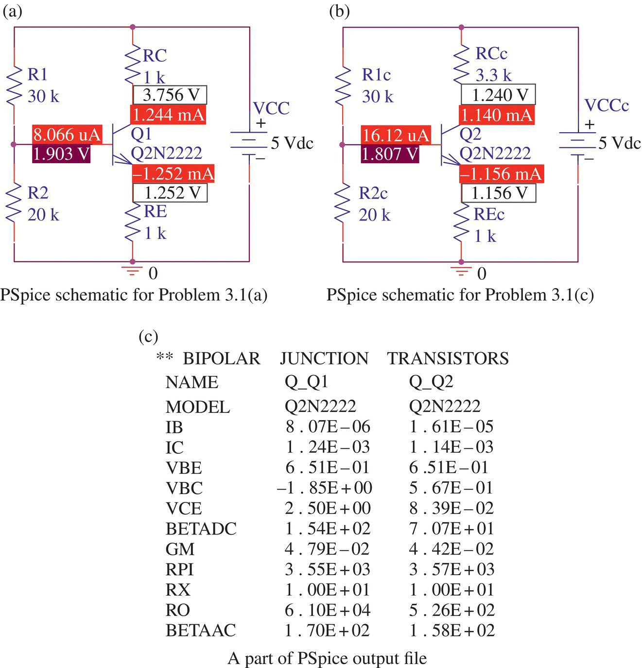
Figure P3.1.2 PSpice simulation results.
BJT_DC_analysis(VCC,R1,R2,RC,RE,[betaF,betaR]);and once (based on the exponential model) by using
BJT_DC_analysis(VCC,R1,R2,RC,RE,[betaF,betaR,Is]); - Noting that vCE = 0.3 V at the edge of saturation, find such a value of RC that Q1 is just barely saturated where RE = 1 kΩ and VCC = 5 V.
- Referring to Figure P3.1.1(c), find iB, iC, and vCE of the circuit with RC = 3.3 kΩ, RE = 1 kΩ, and VCC = 5 V by hand. Then do the same thing two times, once (based on the PWL model) by using
BJT_DC_analysis(VCC,R1,R2,RC,RE,[betaF,betaR]);and once (based on the exponential model) by using
BJT_DC_analysis(VCC,R1,R2,RC,RE,[betaF,betaR,Is]); - Referring to Figure P3.1.2, perform the PSpice simulation to see if the above two analysis results are fine and compare the results with the corresponding MATLAB analysis results.
- Referring to Figure P3.1.1(b), find iC and vCE of the circuit with RC = 1 kΩ, RE = 1 kΩ, and VCC = 5 V by hand. Then do the same thing two times, once (based on the piecewise linear [PWL] model) by using
- 3.2 Circuit with an NPN‐BJT Reverse Biased
Consider the BJT biasing circuit in Figure P3.2.1(a) where the device parameters of the BJT Q1 are βF = 154, βR = 6.092, and Is(saturation current) = 14.34−15 A. Note that the roles of the collector and emitter terminals of a BJT are switched when the BJT is reverse biased.
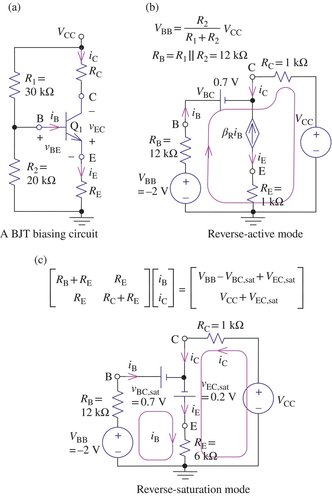
Figure P3.2.1 A BJT biasing circuit and its equivalents in different operation modes (regions) of BJT.
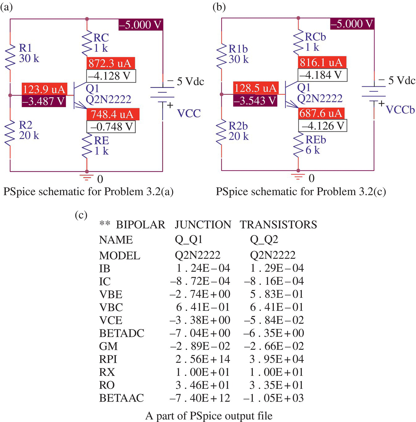
Figure P3.2.2 PSpice simulation results.
- Referring to Figure P3.2.1(b), find iC and vEC of the circuit with RC = 1 kΩ, RE = 1 kΩ, and VCC = −5 V by hand. Then do the same thing two times, once (based on the PWL model) by using
BJT_DC_analysis(VCC,R1,R2,RC,RE,[betaF,betaR]);or
BJT_DC_analysis(VCC,VBB,RB,RC,RE,[betaF,betaR]);and once (based on the exponential model) by using
BJT_DC_analysis_exp(VCC,R1,R2,RC,RE,[betaF,betaR,Is]); - Referring to Figure P3.2.1(c), find iC and vEC of the circuit with RC = 1 kΩ, RE = 6 kΩ, and VCC = −5 V by hand. Then do the same thing two times, once (based on the PWL model) by using
BJT_DC_analysis(VCC,R1,R2,RC,RE,[betaF,betaR]);and once (based on the exponential model) by using
BJT_DC_analysis(VCC,R1,R2,RC,RE,[betaF,betaR,Is]); - Referring to Figure P3.2.2, perform the PSpice simulation to see if the above two analysis results are fine and compare the results with the corresponding MATLAB analysis results.
- Referring to Figure P3.2.1(b), find iC and vEC of the circuit with RC = 1 kΩ, RE = 1 kΩ, and VCC = −5 V by hand. Then do the same thing two times, once (based on the PWL model) by using
- 3.3 Circuit with PNP‐BJT
Consider the PNP‐BJT biasing circuit in Figure P3.3.1(a) where the device parameters of the PNP‐BJT Q1 are βF = 100, βR = 1, and Is(saturation current) = 10 × 10−15 A, respectively.
- Referring to Figure P3.3.1(b), find iC and vEC of the circuit with RC = 1 kΩ, RE = 1 kΩ, and VEE = 5 V by hand. Then do the same thing two times, once (based on the PWL model) by using
BJT_PNP_DC_analysis(VEE,R1,R2,RE,RC,[betaF,betaR]);and once (based on the exponential model) by using
BJT_DC_analysis_exp([VCC VEE],R1,R2,RC,RE, -[betaF, betaR,Is]); - Noting that vEC = 0.3 V at the edge of saturation, find such a value of RC that Q1 is just barely saturated where RE = 1 kΩ and VEE = 5 V.
- Referring to Figure P3.3.1(c), find iC and vEC of the circuit with RC = 3.2 kΩ, RE = 1 kΩ, and VEE = 5 V by hand. Then do the same thing two times, once (based on the PWL model) by using
BJT_PNP_DC_analysis(VEE,R1,R2,RE,RC,[betaF,betaR]);and once (based on the exponential model) by using
BJT_DC_analysis_exp([VCC VEE],R1,R2,RC,RE, -[betaF, betaR,Is]); - Referring to Figure P3.3.1(d), find iC and vCE of the circuit with RC = 1 kΩ, RE = 1 kΩ, and VEE = −5 V by hand. Then do the same thing two times, once (based on the PWL model) by using
BJT_PNP_DC_analysis(VEE,R1,R2,RE,RC,[betaF,betaR]);and once (based on the exponential model) by using
BJT_DC_analysis_exp([VCC VEE],R1,R2,RC,RE,[betaF,betaR,Is]);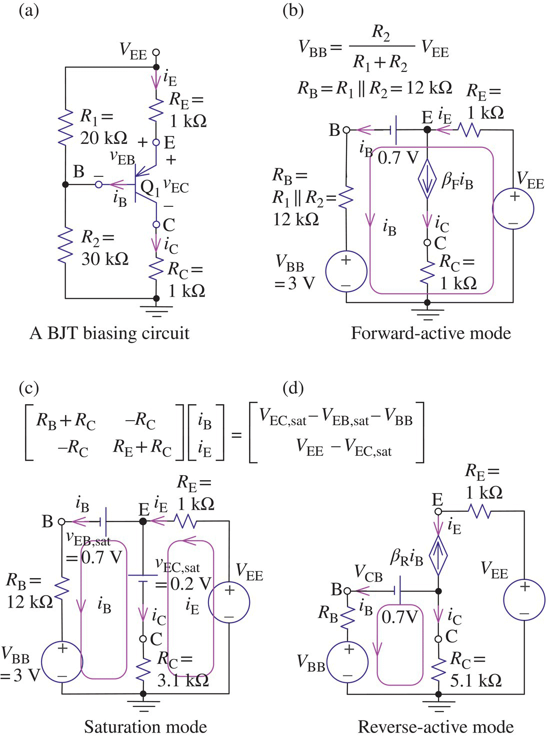
Figure P3.3.1 A PNP‐BJT biasing circuit and its equivalents in different operation modes (regions) of BJT.
- Referring to Figure P3.3.2, perform the PSpice simulation to see if the above three analysis results are fine by comparing the results with the corresponding MATLAB analysis results obtained above. Note that the device parameters of the NPN‐BJT Q1 (QbreakN) and PNP‐BJT Q2 (QbreakP) picked up from the PSpice library ‘breakout.olb’ should be set in the PSpice Model Editor window as shown in Figure 3.14(b2).
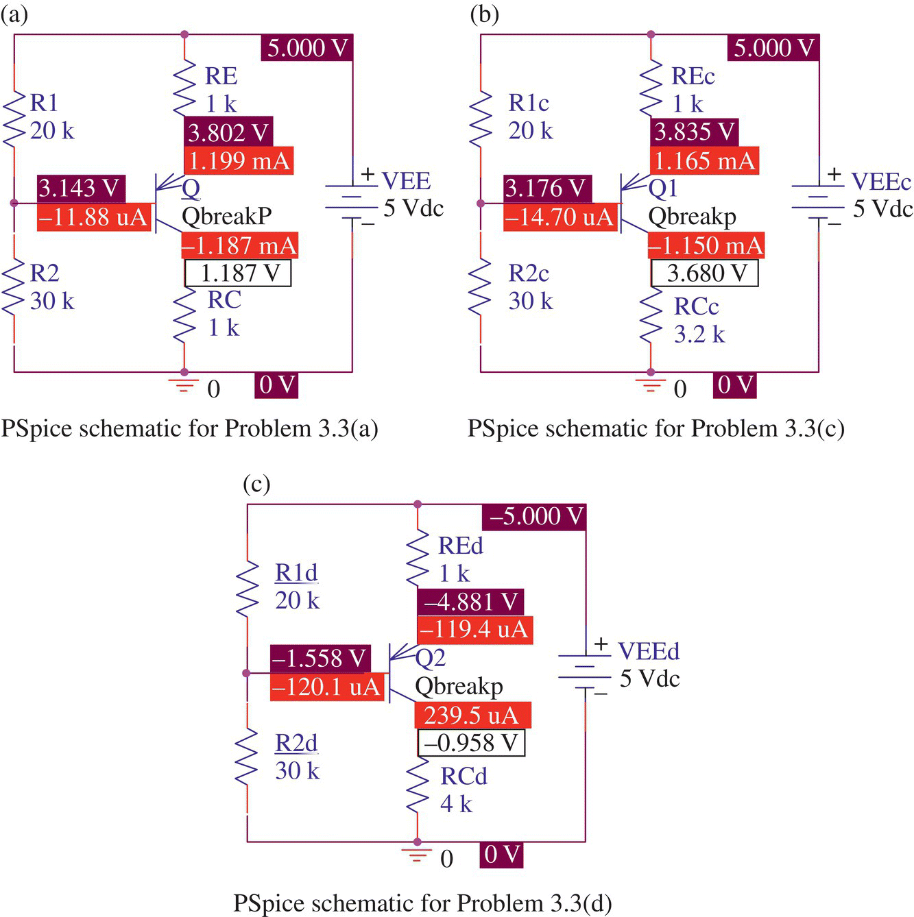
Figure P3.3.2 PSpice simulation results.
- Referring to Figure P3.3.1(b), find iC and vEC of the circuit with RC = 1 kΩ, RE = 1 kΩ, and VEE = 5 V by hand. Then do the same thing two times, once (based on the PWL model) by using
- 3.4 Two‐BJT Circuit
Consider the two‐BJT circuit in Figure P3.4(a) where the device parameters of the BJTs Q1 and Q2 are βF = 100, βR = 1, and Is = 10−14 A in common.
- Referring to Example 3.7, analyze the circuit to find IC1, VEC1, IC2, and VCE2.
- Use the MATLAB function ‘
BJT_PNP_DC_analysis()’/ ‘BJT_DC_analysis()’ to analyze the Q1/Q2 part, respectively. To this end, run the following MATLAB statements:>>betaF=100; betaR=1; Is=1e-14; beta=[betaF betaR];VEE1=10; VCC2=10; R1=3e5; R2=2e5;RE1=55e2; RC1=5e3; RC2=4e3; RE2=4e3;[VB1,VE1,VC1,IB1,IE1,IC1,mode1]= ...BJT_PNP_DC_analysis(VEE1,R1,R2,RE1,RC1,beta);VBB2=???; RB2=???; % Thevenin equivalent of Q1 seen from B2BJT_DC_analysis(VCC2,VBB2,RB2,RC2,RE2,beta);Also, referring to the MATLAB script “elec03e07.m,” complete the above script “elec03p04.m” and run it to do the exponential‐model‐based analysis.
- Referring to Figure P3.4(c), use the PSpice software to simulate the circuit where the device parameters of the NPN‐BJT Q1 (QbreakN) and PNP‐BJT Q2 (QbreakP) picked up from the PSpice library ‘breakout.olb’ should be set in the PSpice Model Editor window as shown in Figure 3.14(b2). Fill Table P3.4 with the PSpice simulation results and the MATLAB analysis results (obtained in (b)). Which one is closer to the PSpice simulation results, the PWL‐model‐based solution or the exponential‐model‐based solution?
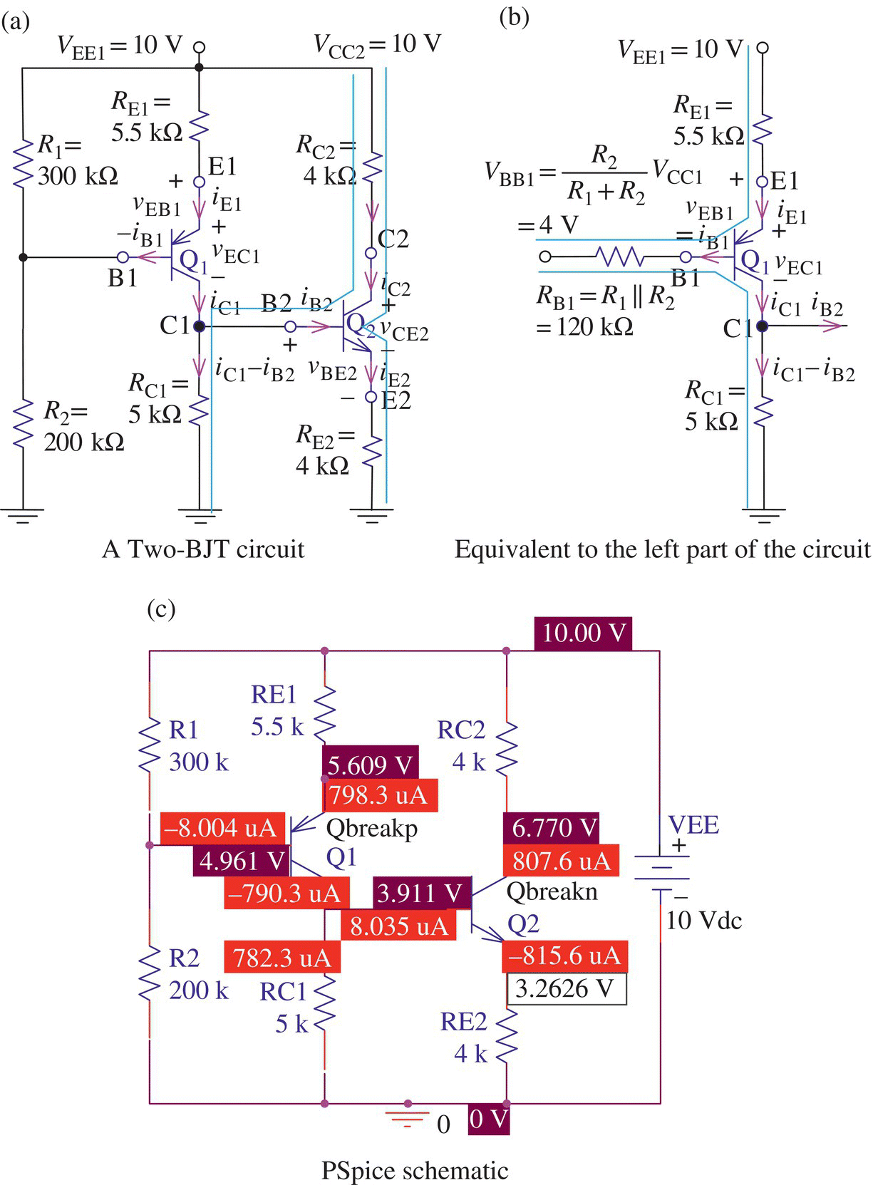
Figure P3.4 A two‐BJT circuit for Problem 3.4.
Table P3.4 MATLAB analysis and PSpice simulation results of BJT circuit in Figure P3.4(a).
IC1 VEC1 IC2 VCE2 PWL model based analysis 0.785 mA Exponential‐model‐based analysis 1.65 V 3.42 V PSpice simulation 0.808 mA - 3.5 Three‐BJT Circuit
Consider the three‐BJT circuit in Figure P3.5(a) where the device parameters of the BJTs Q1, Q2, and Q3 are βF = 100, βR = 1, and Is = 10−14 A in common.
- Analyze the circuit to find IC1, VEC1, IC2, VCE2, IC3, and VEC3. Noting that the Q1‐Q2 part of the circuit is identical to the circuit of Figure P3.4(a), you can copy all the analysis results (except for VC2) of Problem 3.4.
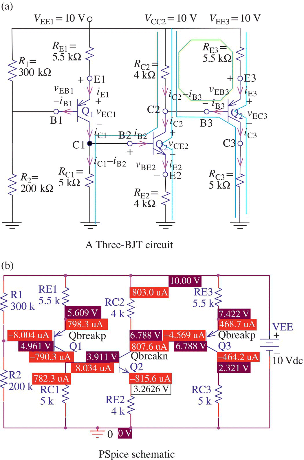
Figure P3.5 A three‐BJT circuit for Problem 3.5.
Table P3.5 MATLAB analysis and PSpice simulation results of the BJT circuit in Figure P3.5(a).
IC1 (mA) VEC1 (V) IC2 (mA) VCE2 (V) IC3 (mA) VCE3 (V) PWL‐model‐based analysis 0.785 1.76 0.788 3.69 0.438 5.37 Exponential‐model‐based analysis 0.795 1.65 0.819 3.42 0.475 4.98 PSpice simulation 0.790 1.70 0.808 3.51 0.464 5.10 - With the analysis result of the Q1/Q2 part (except for VC2) obtained in Problem 3.4, go on to use the MATLAB function ‘
BJT_PNP_DC_analysis()’ for the analysis of the Q3 part. - Referring to Figure P3.5(b), use the PSpice software to simulate the circuit. Fill Table P3.5 with the PSpice simulation results and the MATLAB analysis results (obtained in (b)).
- Analyze the circuit to find IC1, VEC1, IC2, VCE2, IC3, and VEC3. Noting that the Q1‐Q2 part of the circuit is identical to the circuit of Figure P3.4(a), you can copy all the analysis results (except for VC2) of Problem 3.4.
- 3.6 Complementary BJT Pair Circuit
Consider the complementary BJT pair circuit in Figure P3.6.1(a) where the device parameters of the NPN‐/PNP‐BJTs Q1/Q2 are βF = 100, βR = 1, and Is (saturation current) = 10 × 10−15 A. Note that the Kirchhoff's voltage law (KVL) along the mesh B1‐E1‐E2‐B2 yields
(P3.6.1)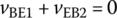
This implies that both vBE1 and vEB2 cannot be positive so that Q1 and Q2 cannot be simultaneously conducting.
- For vi = 10 V, find ii, io, and vo.
- For vi = 5 V, find ii, io, and vo.
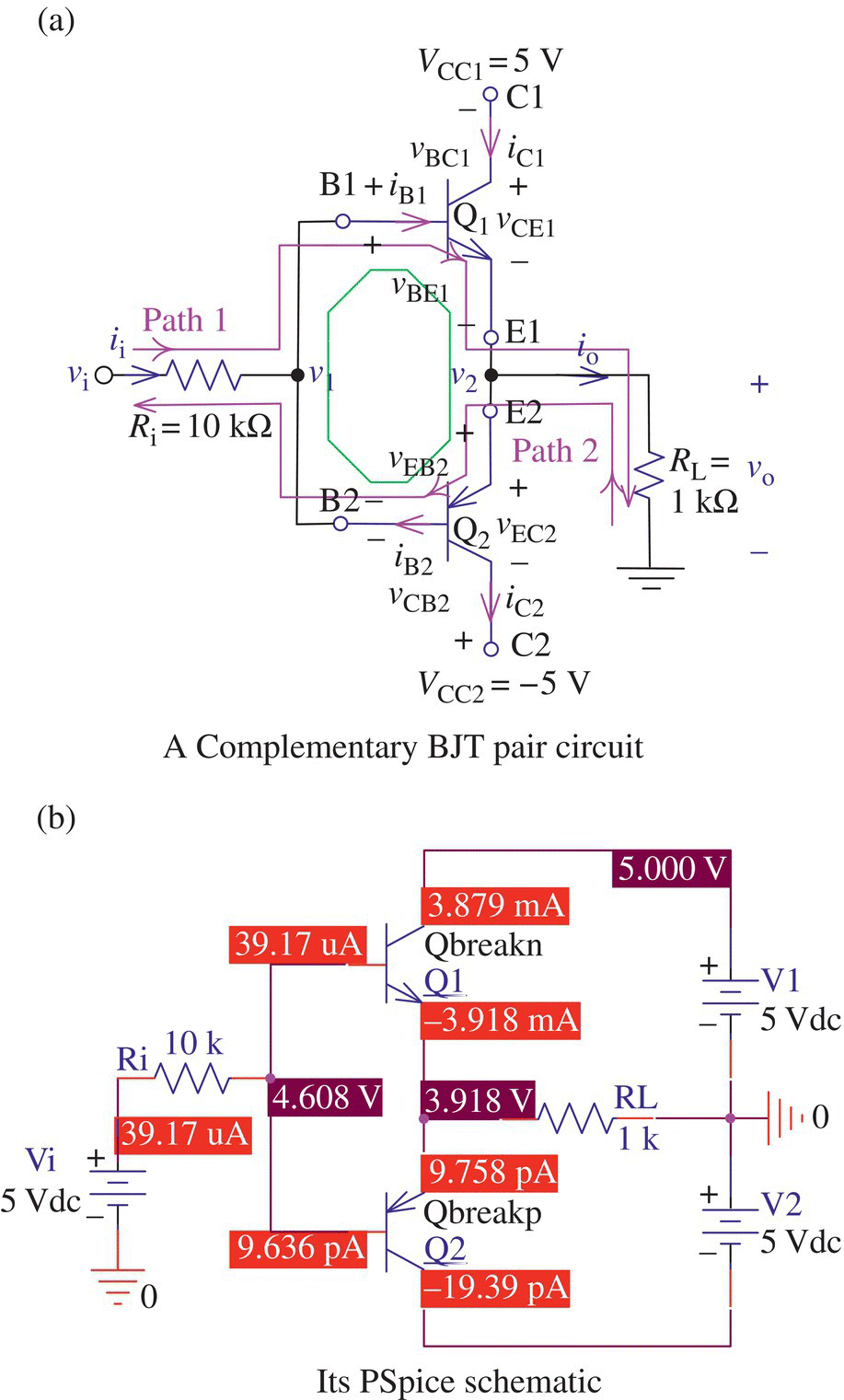
Figure P3.6.1 A BJT biasing circuit and its PSpice schematic.
- For vi = 0 V, find ii, io, and vo.
- For vi = −5 V, find ii, io, and vo.
- For vi = −10 V, find ii, io, and vo.
- Complete the above MATLAB function ‘
BJT2_complementary()’ to analyze the circuit and use it to get ii, io, and vo for vi = {10, 5, 0,−5,−10} by running the following MATLAB statements:>>Ri=1e4; RL=1e3; betaF=100; betaR=1;Is=1e-14; beta=[betaF betaR];VCC1=5; VCC2=-5; VCC=[VCC1 VCC2]; vis=[10 5 0 -5 -10];[vs,iis,ios]=BJT2_complementary(vis,Ri,RL,VCC,beta,Is);fprintf(' vi v1 vo ii io ')disp([vis' vs iis' ios']) - Referring to Figure P3.6.1(b), perform the PSpice simulation with the Analysis type of Bias Point for vi = 5 V.
- Perform the PSpice simulation (with the Analysis type of DC Sweep and Sweep variable Vi) and the MATLAB analysis (using the MATLAB function ‘
BJT2_complementary()’) for vi = [−10:0.02:10]V to get the two graphs shown in Figure P3.6.2, respectively.
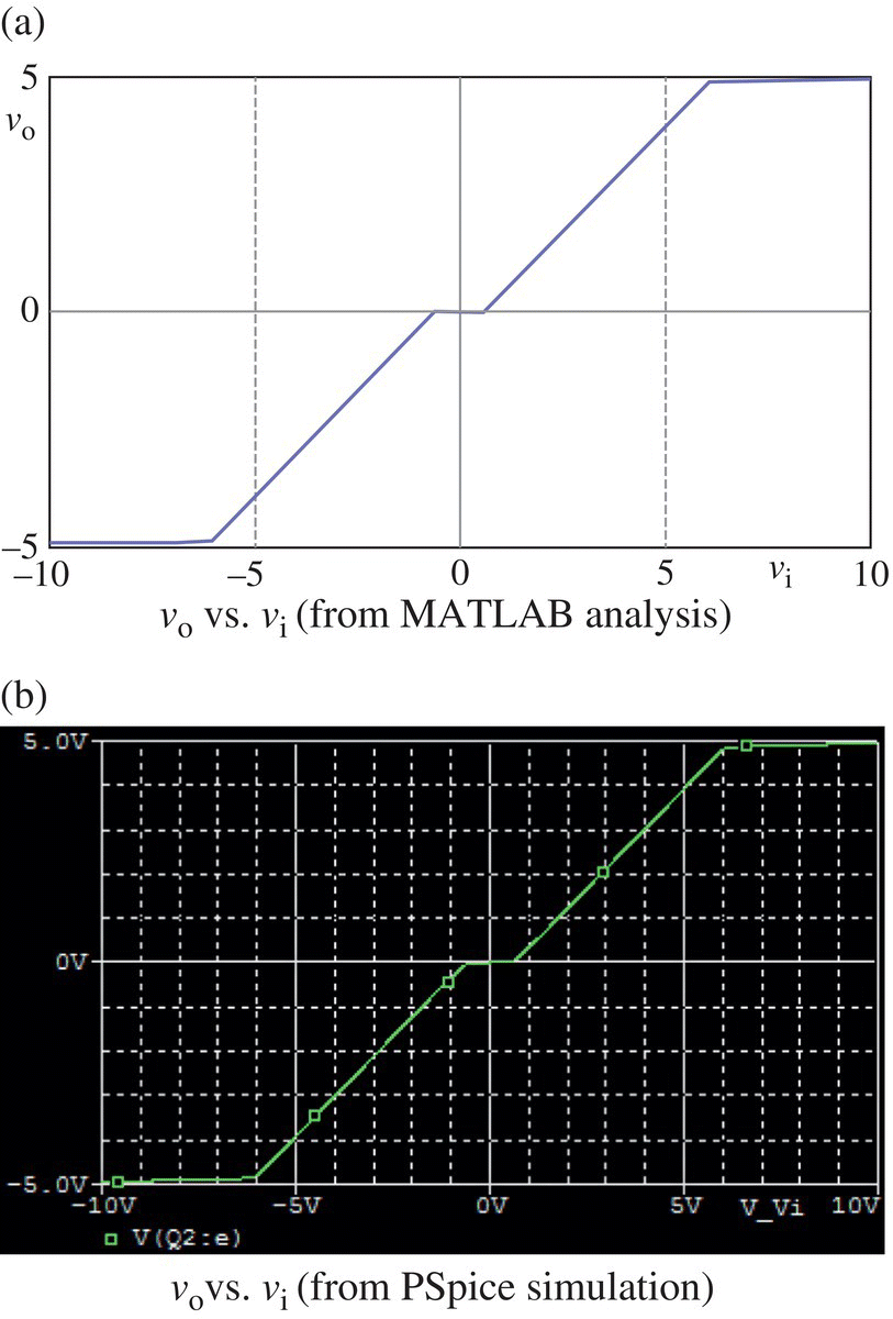
Figure P3.6.2 vo versus vi of the complementary BJT circuit in Figure P3.6.1.
- 3.7 Current Mirror Consisting of Two BJTs
- Consider the current mirror in Figure 3.25(a) where the device parameters of the NPN‐BJTs Q1 and Q2 are βF = 100, βR = 1, and Is (saturation current) = 10 × 10−15 A in common. Referring to the MATLAB function ‘
BJT3_current_mirror()’ presented in Section 3.1.9, compose a MATLAB function ‘BJT2_current_mirror()’ and use it to get io = iC2 for V1 = 15 V and V2 = {1, 5, 10, 20, 40} by running the following MATLAB statements:>>betaF=100; betaR=1; Is=1e-14; beta=[betaF betaR];R=1e4; V1=15; V2=[1 5 10 20 40];io=BJT2_current_mirror(beta,Is,R,[V1 V2]) - Consider the current mirror in Figure P3.7(a) where the device parameters of the NPN‐BJTs Q1, Q2, and Q3 are βF = 100, βR = 1, and Is (saturation current) = 10 × 10−15 A in common. Show that the output current io = iC3 is determined as
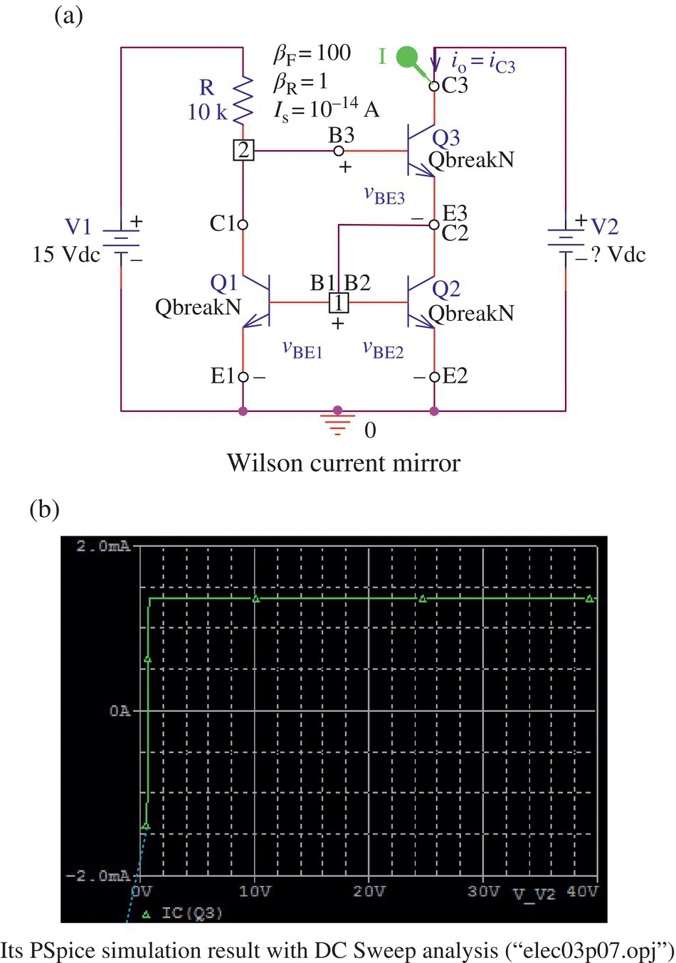
Figure P3.7 Wilson current mirror.
(P3.7.1)
This is supported by the PSpice simulation result (with DC Sweep analysis) shown in Figure P3.7(b). However, why is the output current negative for V2 < 0.66 V?
- Referring to the MATLAB function ‘
BJT3_current_mirror()’ presented in Section 3.1.9, compose a MATLAB function ‘BJT3_current_mirror_Wilson()’ to analyze the current mirror of Figure P3.7(a) and use it to get the plot of io = iC3 versus V2 = {0:0.01: 40} for V1 = 15 V.
- Consider the current mirror in Figure 3.25(a) where the device parameters of the NPN‐BJTs Q1 and Q2 are βF = 100, βR = 1, and Is (saturation current) = 10 × 10−15 A in common. Referring to the MATLAB function ‘
- 3.8 BJT Inverter
Consider the BJT inverter in Figure P3.8(a) or 3.27(a) where the device parameters of the NPN‐BJT Q are βF = 100, βR = 1, and Is (saturation current) = 10 × 10−15 A.
- Complete the following approximate vi‐vo relationship and find the approximate slope of the VTC of the inverter with the BJT Q1 operating in the forward‐active mode:
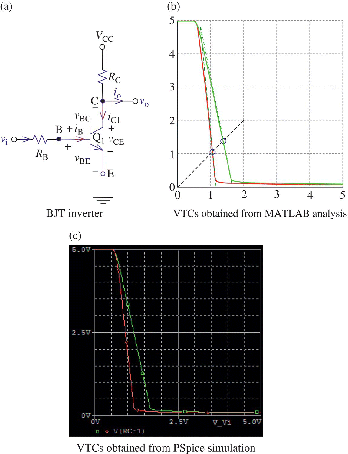
Figure P3.8 A BJT inverter and its voltage transfer characteristic curves (VTCs) obtained using MATLAB/PSpice.
- Complete the following MATLAB script “elec03p08b.m,” which uses the MATLAB function ‘
BJT_inverter()’ presented in Section 3.1.10 to plot the VTCs and their linear approximations for RB = 10 kΩ/20 kΩ where RC = 1 kΩ and VCC = 5 V as shown in Figure P3.8(b). - Perform the PSpice simulation (with the Analysis type of DC Sweep and Sweep variable Vi) to plot the VTCs for RB = 10 kΩ/20 kΩ where RC = 1 kΩ and VCC = 5 V as shown in Figure P3.8(c). Note that to have multiple waveforms (obtained from different simulations) plotted in a single graph in the Probe (PSpice A/D) window, select File>Append_Waveform(.DAT) on the menu bar to pick up the existing data file(s). If you want to save a data file obtained from the current simulation, say, to plot it together with another data (to be obtained afterward), rename the data file appropriately, which can be located by selecting the menu File>Append_Waveform(.DAT).
- 3.9 ECL (Emitter‐Coupled Logic) – Differential Pair
Consider the two BJT differential pairs, called emitter‐coupled logic (ECL), each in Figure P3.9(a1) and (a2) where the device parameters of all the NPN‐BJTs are βF = 100, βR = 1, and Is (saturation current) = 10 × 10−15A in common.
- Referring to Eq. (3.1.72), which shows vo1 and vo2 of the ECL in Figure 3.29, and assuming that both BJTs Q1 and Q2 operate in the forward active region, complete the following expressions (in terms of the differential input voltage vi) for vo1 and vo2 of the ECL in Figure P3.9(a1):

Figure P3.9 Two ECLs, one with two BJTs and another with four BJTs, and their output waveforms.
(P3.9.1a) (P3.9.1b)
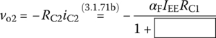
- Compared with the ECL in Figure P3.9(a1), the ECL in Figure P3.9(a2) has two more BJTs Q3 and Q4 that are expected to shift vo1 and vo2 (up/down) by one base‐emitter drop VBE3 ≈ 0.6 V and VBE4 ≈ 0.6 V, respectively, as can be seen by comparing the output waveforms of Figure P3.9(b1) and (b2) (MATLAB analysis results) or c1 and c2 (PSpice simulation results).
- To analyze the ECL circuit of Figure P3.9(a1) using the exponential model of BJT, apply KVL across each of RC1 and RC2 and apply KCL at node 3 to write the following equations:
(P3.9.2a) (P3.9.2b)
 (P3.9.2c)
where iCk(vBEk,vBCk) and iBk(vBEk,vBCk) are defined by Eqs. (3.1.23a,b), and iEk(˖,˖) = iBk(˖,˖) + iCk(˖,˖) for all k. Then complete the above MATLAB function ‘
ECL1()’ so that it can analyze the ECL and run the following statements to plot the output waveforms as shown in Figure P3.9(b1).>>betaF=100; betaR=1; Is=1e-14; RC=2e3; IEE=3e-4;Vref=-0.9; VEE=-5.2;ECL1([betaF betaR],Is,RC,IEE,Vref,VEE);- To analyze the ECL circuit of Figure P3.9(a2) using the exponential model of BJT, apply KVL across each of RC1, RC2, R1, and R2 and apply KCL at node 5 to write the following equations:
(P3.9.3c)
 (P3.9.3d)
 (P3.9.3a)
 (P3.9.3b)
 (P3.9.3e)
where iCk(vBEk,vBCk) and iBk(vBEk,vBCk) are defined by Eqs. (3.1.23a,b), and iEk(+,+) = iBk(+,+) + iCk(+,+) for all k. Then complete the above MATLAB function ‘
ECL2()’ so that it can analyze the ECL and run the following statements to plot the output waveforms as shown in Figure P3.9(b2).>>betaF=100; betaR=1; Is=1e-14; RC=2e3; IEE=3e-4; Vref=-0.9; VEE=-5.2;RC=2e3; R=42e3; IEE=3e-4; Vref=-0.9; VEE=-5.2;ECL2([betaF betaR],Is,RC,R,IEE,Vref,VEE);
- Referring to Eq. (3.1.72), which shows vo1 and vo2 of the ECL in Figure 3.29, and assuming that both BJTs Q1 and Q2 operate in the forward active region, complete the following expressions (in terms of the differential input voltage vi) for vo1 and vo2 of the ECL in Figure P3.9(a1):
- 3.10 CB Amplifier
Consider the CB amplifier in Figure P3.10(a1) or (a2) where the device parameters of the NPN‐BJT are βF = 100, βR = 1, βAC = 100, rb = 0 Ω, and Is = 10 × 10−15 A.
- Complete the following MATLAB script “elec03p10.m” and run it to find the overall voltage gain Gv and input/output resistances Ri/Ro. Is the result of DC analysis using the PWL model of BJT closer to the PSpice simulation result shown in the schematic (Figure P3.10(a1) or (a2)) than that using the exponential model?
Figure P3.10 A CB amplifier and its PSpice simulation result (“elec03p10.opj”).
- Are the values of Gv, Ri, and Ro close to those obtained from the PSpice simulations shown in Figure P3.10(b1), (b2), and (b3)?
- Complete the following MATLAB script “elec03p10.m” and run it to find the overall voltage gain Gv and input/output resistances Ri/Ro. Is the result of DC analysis using the PWL model of BJT closer to the PSpice simulation result shown in the schematic (Figure P3.10(a1) or (a2)) than that using the exponential model?
- 3.11 CC Amplifier
Consider the CC amplifier in Figure P3.11(a1) or (a2) where the device parameters of the NPN‐BJT are βF = 100, βR = 1, βAC = 100, rb = 0 Ω, and Is = 10 × 10−15 A.
- Complete the following MATLAB script “elec03p11.m” and run it to find the overall voltage gain Gv and input/output resistances Ri/Ro. Is the result of DC analysis using the PWL model of BJT close to that using the exponential model?
- Are the values of Gv, Ri, and Ro close to those obtained from the PSpice simulation shown in Figure P3.11(b1), (b2), and (b3)?
Figure P3.11 A CC amplifier and its PSpice simulation result (“elec03p11.opj”).
- 3.12 Two‐Stage BJT Amplifier
Consider the two‐stage BJT amplifier in Figure P3.12(a) where the device parameters of the NPN‐BJT Q are βF = 100, βR = 1, βAC = 100, and rb = 0 Ω. Complete the following MATLAB script “elec03p12.m” and run it to find the overall voltage gain Gv and output resistance Ro2.
- (Note) As long as no CC amplifier (whose input/output resistances are affected by the input/output resistances of the next/previous stage, respectively) is involved, it will be enough to analyze each stage starting from the last one with the source resistance of every stage (except for the first one having the true value of Rs) set to 0 and with the load resistance of every stage (except for the last one having the true value of RL) set to the input resistance of the next stage.
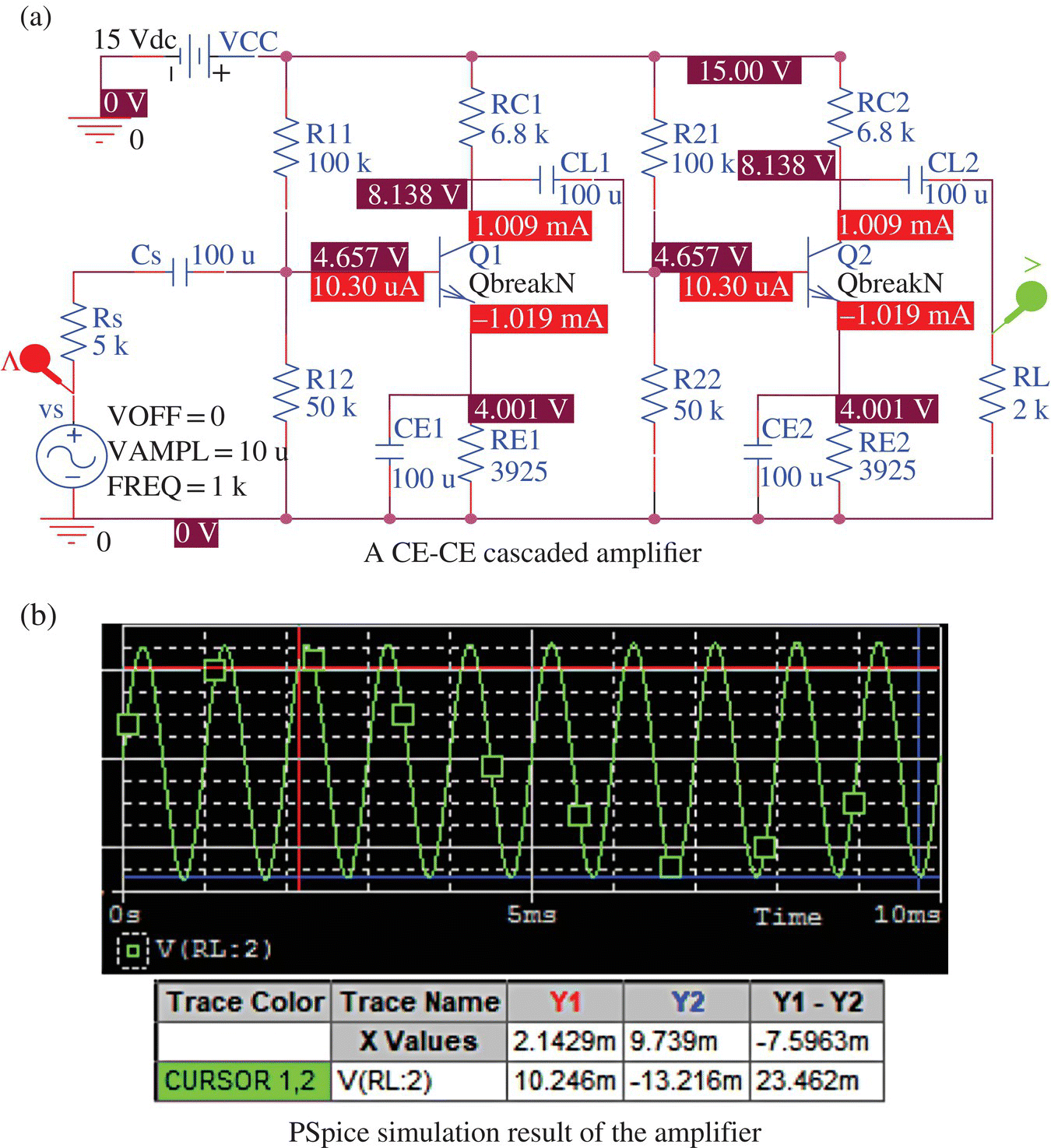
Figure P3.12 A two‐stage BJT amplifier and its PSpice simulation result (“elec03p12.opj”).
- 3.13 Three‐Stage BJT Amplifier
Consider the three‐stage BJT amplifier in Figure P3.13.1(a) where the device parameters of all the NPN‐BJTs are βF = 100, βR = 1, βAC = 100, rb = 0 Ω, and Is = 1 × 10⁻¹⁶ A in common. Note that the first two stages are identical to those of the amplifier in Figure P3.13(a), whose overall voltage gain and output resistance are Gv12 = 1329.8 and Ro2 = 6795 Ω, respectively.
- Complete the above MATLAB script “elec03p13.m” and run it to find the overall voltage gain Gv, and the voltage gains (Avk's) and input/output resistances (Rik/Rok's) of each stage k. Is the value of Gv close to that obtained from the PSpice simulation shown in Figure P3.13.1(b1)? If you are not satisfied, try with the exponential model of BJT.
- Determine the values of the open‐loop voltage gains {Av1_o, Av2_o, Av3_o} (with Ri2 = ∞, Ri3 = ∞, and RL = ∞ to exclude its next stage) and the output resistances {Ro1_0, Ro2_0, Ro3_0} (with Rs = 0, Rs2 = 0, and Rs3 = 0 to exclude its previous stage) of each stage. Check if the following relations hold between the voltage gains {Av1, Av2, Av3} (considering the next stage) and the open‐loop voltage gains {Av1_o, Av2_o, Av3_o}:
(P3.13.1)

- Do you see that Rok_0≠Rok for any stage k? Why is that?
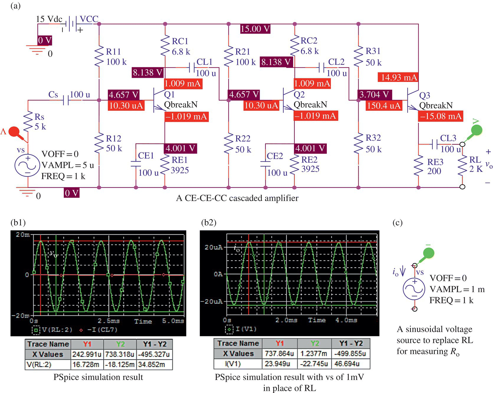
Figure P3.13.1 A three‐stage BJT amplifier and its PSpice simulation result (“elec03p13.opj”).
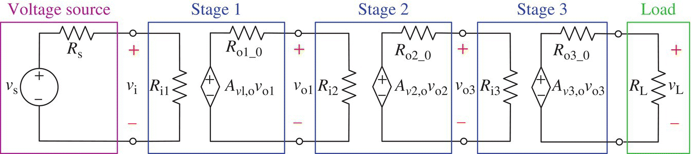
Figure P3.13.2 A voltage source model for the CE‐CE‐CC amplifier of Figure P3.13.1.
- With the values of Rok_0's and Rik's together with the open‐loop voltage gain Avk_o's for k = 1, 2, and 3 (obtained in (b)), complete the voltage source model of the three‐stage amplifier (Figure P3.13.2) and find the overall voltage gain.
- Use the voltage source model to determine the overall voltage gain Gv12 of the CE‐CE stage (with the CC stage removed). Is it smaller than Gv in spite of not having a CC stage with voltage gain Av3 = 0.991 smaller than 1? Why is that?
- Figure P3.13.1(b2) shows another PSpice simulation result on the current io for the PSpice schematic with RL replaced by a sinusoidal voltage source of 1 mV (Figure P3.13.1(c)) and the original voltage source short‐circuited for removal. From the simulation result, find the output resistance Ro and see if it is close to the theoretical value obtained in (a).
- 3.14 Design of CE Amplifier Circuit
Consider the CE BJT amplifier circuit of Figure 3.52.1(a) where the forward DC/AC current gains, reverse DC current gain, and base resistance of the BJT are βF = 162/βAC = 176, βR = 6, and rb = 10 Ω, respectively.
- Considering the load resistance RL = 50 kΩ, determine such resistor values that the voltage gain Av,d = −20 can be achieved with the operating point located near Q1 = (VCE,Q,IC,Q) = (3 V, 2 mA). Analyze the designed circuit with source/load resistance Rs = 50 Ω/RL = 50 kΩ to find the voltage gain Av. Is it close to Av,d = −20?
(Hint) How about running the following MATLAB statements?
>>bF=162; bR=6; bAC=176; rb=10; T=27; % Device constantsVCC=12; Rs=50; RL=5e4; % Circuit constantsAvd=20; VCEQd=3; KC=VCEQd/VCC;ICQd=2e-3; % Design constants [R1,R2,RC,RE1,RE2]=...BJT_CE_design(VCC,[bF bAC],rb,Avd,ICQd,RL,T,KC);Vsm=0.1; beta=[bF bR bAC];[VBQ,VEQ,VCQ,IBQ,IEQ,ICQ,Av]=...BJT_CE_analysis(VCC,rb,Rs,R1,R2,RC,[RE1 RE2],RL,beta,Vsm) - Referring to Figure P3.14(a), perform the PSpice simulation of the designed CE amplifier with Time‐Domain Analysis to see the output voltage vo(t) to an AC input vs(t) = Vsm sin (2000πt) (with Vsm = 0.05 V) for 2 ms (with maximum step size 1 us). Is the voltage gain Vom,p‐p/2Vsm close to Av obtained in (a)? Also, on the collector characteristic curves of BJT Q2N2222 (used in the CE amplifier), draw the load line to find the operating point (VCE,Q, IC,Q) and check if it agrees with the analysis result (obtained in (a)) and PSpice simulation result.
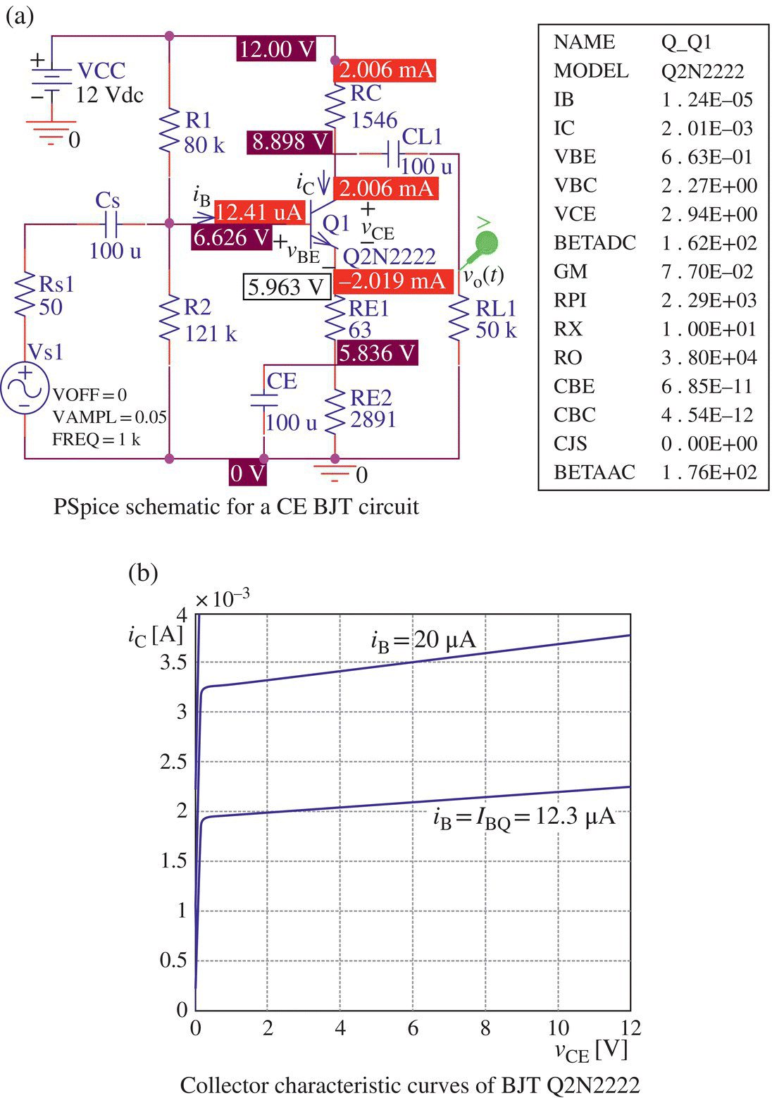
Figure P3.14 A CE BJT circuit and the collector characteristic curves of BJT Q2N2222 (“elec03p14.opj”).
- Perform the PSpice simulation of the designed CE amplifier twice more to see the output voltage vo(t) to an AC input vs(t) = Vsm sin (2000πt) with larger small‐signal input amplitudes Vsm = 0.15 V and 0.2 V. If the output voltage waveforms are distorted on the upper/lower part, discuss the reason of the distortion in connection with the possibility of the (dynamic) operating point (moved by the small‐signal input) to enter the cutoff/saturation region. Does the MATLAB function ‘
BJT_CE_analysis()’ (with the input voltage amplitude Vsm = 0.15/0.2 given as the 10th input argument) give you appropriate warning messages about the possibility of saturation or cutoff regions? - To reduce the distortion of vo(t), change the resistor values so that the operating point can be located at Q2 = (VCE,Q, IC,Q) = (4 V, 2 mA) and Q3 = (VCE,Q, IC,Q) = (5 V, 4 mA). Perform the PSpice simulation of the designed CE amplifiers to see the output voltage vo(t) to an AC input vs(t) = Vsm sin (2000πt) with Vsm = 0.2 V. Discuss the relationship between the static operating point location and the possibility of distortion.
- Considering the load resistance RL = 50 kΩ, determine such resistor values that the voltage gain Av,d = −20 can be achieved with the operating point located near Q1 = (VCE,Q,IC,Q) = (3 V, 2 mA). Analyze the designed circuit with source/load resistance Rs = 50 Ω/RL = 50 kΩ to find the voltage gain Av. Is it close to Av,d = −20?
- 3.15 Frequency Response of a BJT Cascode Amplifier
Consider the BJT cascode amplifier with PSpice schematic and simulation result on the frequency response in Figure P3.15(a) and (b), respectively, where VCC = 12 V, Rs = 50 Ω, Cs = 100 μF, R1 = 100 kΩ, R2 = 100 kΩ, R3 = 50 kΩ, RE = 2 kΩ, CE = 100 μF, CB = 100 μF, RC = 3 kΩ, CL = 1 μF, RL = 100 kΩ, CLL = 1 nF, and the values of the BJT parameters of the (high‐frequency) small‐signal equivalent in Figure P3.15(d) (based on the model in Figure 3.18) are βF = 100, βR = 1, βAC = 100, VA = 104 V, Is = 10−14 A, rb = 0 Ω, Cbe(Cje) = 10 pF, and Cbc(Cjc) = 1 pF.
- Complete the following MATLAB function ‘
BJT_cascode_DC_analysis()‘, which performs the DC analysis of the BJT cascade amplifier to determine the node voltages and base/collector currents at the operating point.
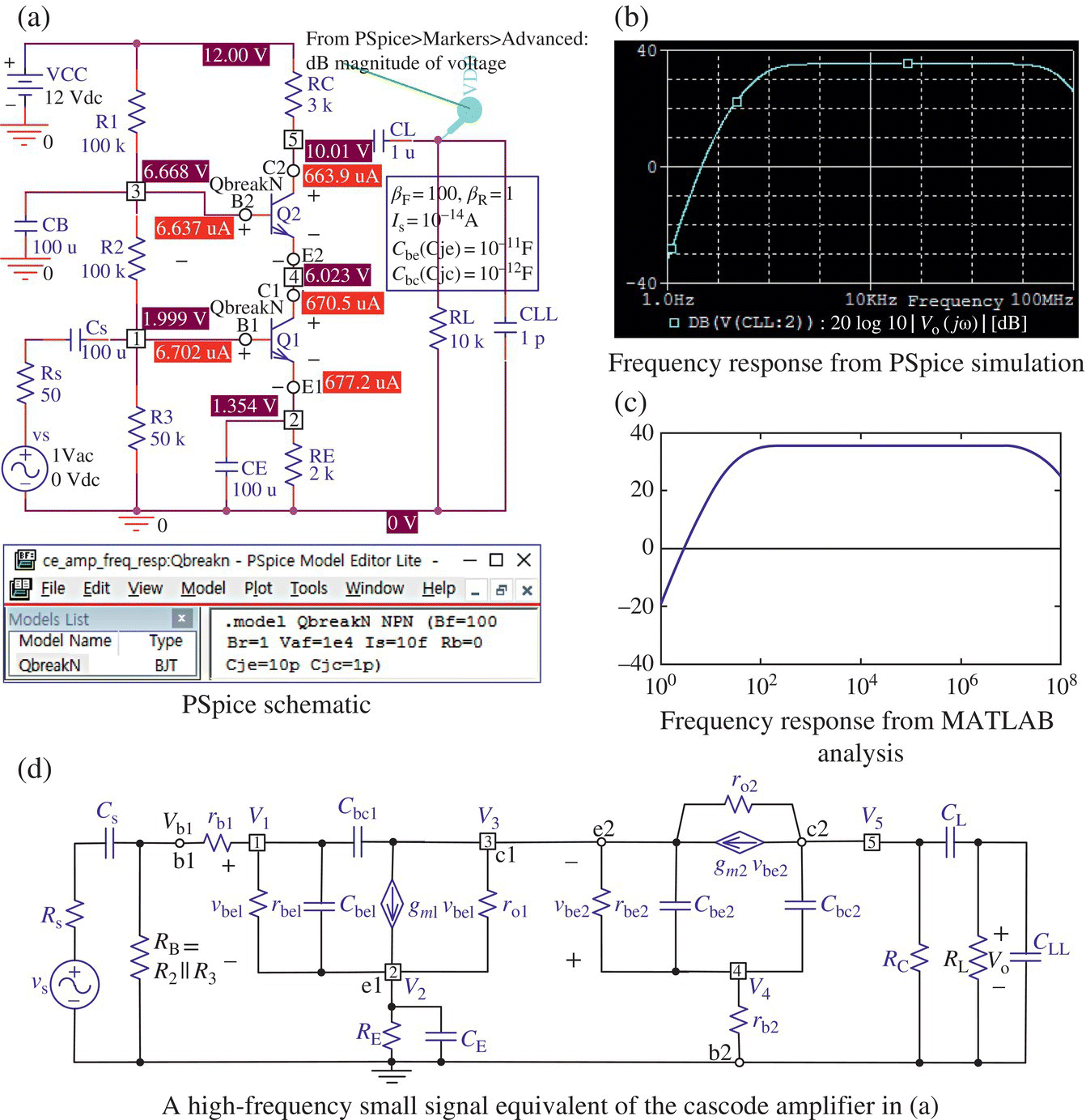
Figure P3.15 A cascode amplifier circuit and its frequency response from PSpice and MATLAB (“elec03p15.opj”).
- Complete the above MATLAB function ‘
BJT_cascode_xfer_ftn()’, which solves a set of four or five node equations for the high‐frequency small‐signal equivalent (Figure P3.15(d)) (depending on rbe=0 or not) to find the transfer function G(s) = Vo(s)/Vs(s) of the cascade amplifier. - Complete the above MATLAB script “elec03p15.m” and run it to perform the DC analysis (using ‘
BJT_cascode_DC_analysis()’), then based on the DC analysis result, use ‘BJT_cascode_xfer_ftn()’ to find the transfer function G(s), and plot the frequency response magnitude 20log10|G(jω)| [dB] of the cascade amplifier versus f = 1∼100 MHz as shown in Figure P3.15(c). - Perform the PSpice simulation (with AC Sweep analysis) to get the frequency response magnitude curve as shown in Figure P3.15(b). Is the Bias Point analysis result (obtained as a by‐product) close to the DC analysis result obtained by using ‘
BJT_cascode_DC_analysis()’ in (c)?
- Complete the following MATLAB function ‘
- 3.16 Time Response of a BJT Inverter with another Inverter as a Load
Consider the BJT inverter in Figure P3.16(a) where VCC = 12 V, RB = 1 kΩ, RC = 5 kΩ, RC1 = 5 kΩ, and the BJT parameters are
- βF = 100, βR = 1, Is = 10−14 A, rb = 0 Ω, VA = ∞V, Cbe1(Cje) = 10 pF, and Cbc1(Cjc) = 1 pF or 10 pF for Q1,
- and βF = 100, βR = 1, Is = 10−14 A, rb = 0 Ω, VA = ∞V, Cbe2(Cje) = 10 pF, and Cbc2(Cjc) = 1 pF for Q2.
Figure P3.16(b1) and (b2) shows the input/output voltage waveforms obtained from PSpice simulations, each with Cbc1=1 pF and 10 pF for Q1, respectively. Referring to Section 3.6 and Figure P3.16(b1‐b2), answer the following questions:
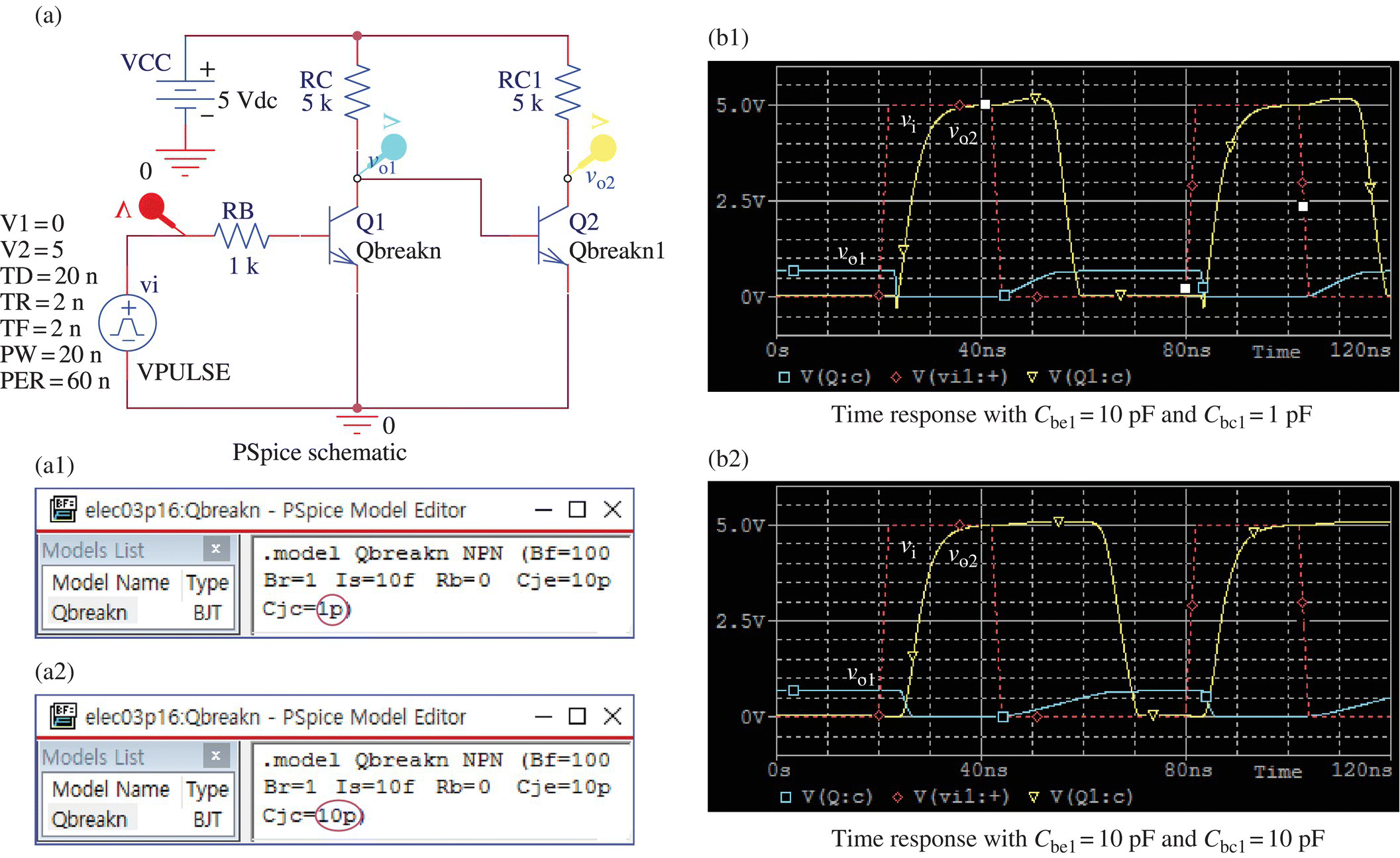
Figure P3.16 BJT inverter with another inverter as a load and its time responses from PSpice (“elec03p16.opj”).
- During the rising period, why does vo1 reach just 0.7 V while vo2 reaches VCC = 5 V?
- The output voltage vo2(t) of the second inverter shows a small negative spike in the beginning of its rising period in Figure P3.16(b1), but not in Figure P3.16(b2). Explain how such a difference is made by the difference in Cbc1 = 1 pF or 10 pF.
- Explain how a larger value of Cbc1 makes a longer time constant of vo1 during its rising period.