4
FET Circuits
4.1 Field‐Effect Transistor (FET)
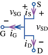
As the Bipolar Junction Transistor (BJT) with three terminals, each called the base B, collector C, and emitter E, the Field‐Effect Transistor (FET) is also a semiconductor device with three terminals, each called the gate G, drain D, and source S. In contrast with the BJT that operates with both types of charge carriers, holes and electrons, the FET is a ‘unipolar’ device that works with only one type of carriers, holes or electrons. While the BJT can basically be modeled as a current‐controlled current source (in the forward‐active region) since its collector current iC depends on its base current iB, the FET can basically be modeled as a voltage(field)‐controlled current source (in the saturation region) since its drain current iD depends on its gate‐to‐source voltage vGS. Table 4.1 shows a rough comparison between BJTs and FETs.
Table 4.1 BJT versus FET.
| FET (Field Effect Transistor) | BJT (Bipolar Junction Transistor) | |
| Voltage‐operated device | Current‐operated device | |
| Input resistance | Large | Small in CE/CB configurations |
| Output resistance | Large | Small |
| Power dissipation | Low | High |
| Noise | Low | Medium |
| Switching time | Very fast | Fast |
| Robustness to static charge | Low (more destructible) | High |
| Thermal stability | Better | |
| Fabricability | FET can be more easily fabricated with higher density in a smaller space. It can also be connected as R or C, which makes possible the design of systems consisting of only FETs with no other elements. | |
Two types of FET are most widely used, junction‐gate device called JFET (Junction FET) and insulated‐gate device called MOSFET (Metal‐Oxide‐Semiconductor FET).
4.1.1 JFET (Junction FET)
There are two basic configurations of junction field effect transistor, the n‐channel JFET and the p‐channel JFET. As shown in Figures 4.1.1 and 4.1.2, an n/p‐channel JFET consists of a lightly doped n/p‐type semiconductor channel and a highly doped P(P+)/N(N+)‐type semiconductor gate. Figure 4.2(a) and (b) show typical drain (output) and transfer characteristic curves of a JFET, respectively. There are three regions (operation modes) besides the breakdown region:
- Ohmic (Triode) region
When 0 < vDS ≤ vGS
−Vt with Vt < vGS < 0 (for an n‐channel JFET), the drain current will be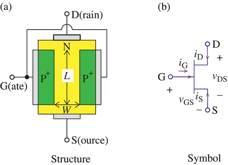
Figure 4.1.1 Structure and symbol of an n‐channel

Figure 4.1.2 Structure and symbol of a p‐channel JFET.
with
 [A/V2]: transconductance coefficient or conduction parameter
where Vt [V], called the threshold, pinch‐off, or pinch‐down voltage, is such a value of vGS that the drain current iD drops to zero if vGS ≤ Vt (for an n‐channel JFET) or vGS ≥ Vt (for a p‐channel JFET). λ [V
‐1] is the channel length modulation (CLM) parameter, typically ranging from 0.005 to 0.02 V‐1, which accounts for the variation of transconductance coefficient with vDS. IDSS [A], called the drain‐to‐source saturation current or zero bias (gate voltage) drain current, is the value of the drain current at vDS =−Vt (with vGS = 0).Why is this region named ‘ohmic region’? Because the JFET in the region acts like a voltage‐controlled resistor whose resistance is determined by vGS. Since iD can be large depending on vGS even with a very low vDS, the JFET operating in this region can be viewed as a closed switch with the on‐drain resistance rDS,ON.
- Saturation (Pinch‐off) or Constant current region
When 0 ≤ vGS − Vt ≤ vDS < Vbreakdown (for an n‐channel MOSFET), the drain current is determined as
Note that the boundary between the ohmic and saturation regions plotted as a line of triangle (∇) symbols is described by
(4.1.3)
- Cutoff region
If vGS ≤ Vt (for an n‐channel JFET) or vGS ≥ Vt (for a p‐channel JFET), the leakage drain current IDS,OFF and the gate cutoff current IGSS flow between the drain/gate and the source of an FET. However, the currents are about 1 pA or less than that even under high voltage, the FET can be viewed as an open switch.
- Breakdown region
If the magnitude of the voltage across any two terminals exceeds a certain value, it may cause avalanche breakdown across the gate junction. As can be seen from the drain (output) characteristics in Figure 4.2(a), the breakdown voltage between drain and source becomes lower as the reverse‐bias gate voltage (|vGS|) increases in magnitude where the breakdown voltage BVDSS with vGS = 0 is specified in the manufacturers' datasheets.
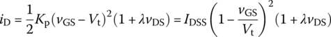
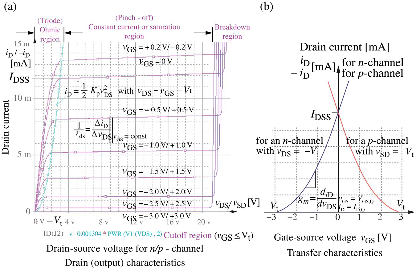
Figure 4.2 Typical characteristics of a JFET.
Figure 4.3 Small‐signal models of FET.
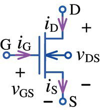
Figure 4.3(a) and (b) shows the high/low frequency small‐signal (AC) models of an FET operating in the saturation region, respectively, where ro[Ω]: incremental resistance between D and S (called the output resistance) is the reciprocal of the slope of the output characteristic (Figure 4.2(a)) at the operating (bias) point Q:
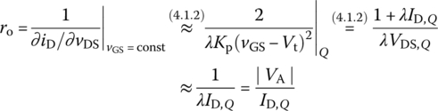
gm[S]: transconductance (gain) is the slope of the transfer characteristic (Figure 4.2(b)) at the operating point Q:
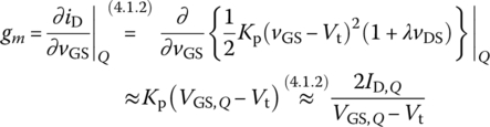
VA[V]: channel modulation voltage or Early voltage normally in the range of 20 ~ 200 V
Note that the parameters KP, lambda, Vto, Cgd, and Cgs of the PSpice model for a JFET represent Kp, λ, Vt, Cgd, and Cgs, respectively, as can be seen from the PSpice Model Editor window (opened by selecting the device and clicking on Edit > PSpice:Model from the top menu bar in the Schematic Window) or the PSpice simulation output file. Also, the operating point information in the PSpice simulation output file obtained from the Bias Point analysis shows the parameters GM and GDS, each representing gm and 1/ro.
Let us consider the JFET circuit of Figure 4.4(a1) where the voltage appearing across RS is fed back to bias the JFET. Note that RS should be chosen large enough to make vGS < 0 so that the gate‐channel(source) junction can be reverse‐biased for normal operation. To analyze this circuit, let us apply Kirchhoff's voltage law (KVL) to the G‐S loop to write the load line equation and solve it to find iD as
Then, assuming that the FET will be in the saturation region, we equate this to the drain current Eq. (4.1.2) with λ ≈ 0:

where vG = 0, RD = 1 kΩ, RS = 500 Ω, VDD = 10 V, VSS = −1 V, Kp = 2.608 × 10‐3 A/V2, Vt = −3 V, and IDSS = ![]() . We solve Eq. (4.1.6) to find VGS,Q =
. We solve Eq. (4.1.6) to find VGS,Q = −1.17 V and substitute it for vGS into Eq. (4.1.5) to get ID,Q = 4.35 mA, which is supported by the operating point Q = (VGS,Q, ID,Q) = (‐1.17 V, 4.35 mA) obtained from the load line analysis shown in Figure 4.4(b). We can substitute ID,Q = 4.35 mA into the KVL equation for the D‐S loop to find VDS,Q:
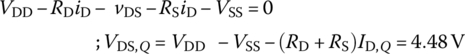

Figure 4.4 DC analysis of a JFET circuit
These computations can be done by running the following MATLAB statements:
>>vG=0; RD=1000; RS=500; VDD=10; VSS=-1; Kp=2.608e-3;Vt=-3; IDSS=Kp/2*Vt^2>>x=roots([Kp/2 1/RS-Kp*Vt Kp/2*Vt^2+(VSS-vG)/RS]); % Eq. (4.1.6)>>VGSQ=x(find((Vt<x&x<vG-VSS)|(Vt>x&x>vG-VSS)))VGSQ = -1.1740>>IDQ=(vG-VSS-VGSQ)/RS % Eq. (4.1.5)IDQ = 0.0043>>VDSQ=VDD-VSS-(RD+RS)*IDQ % Eq. (4.1.7)VDSQ = 4.4780
As an alternative, the MATLAB function ‘FET_DC_analysis()’ (that was made to analyze the standard FET biasing circuits using a voltage divider as depicted in Figure 4.4(a2)) can be used as follows:
>>R1=1e12; R2=1e5; [VGQ,VSQ,VDQ,VGSQ,VDSQ,IDQ,mode]=...FET_DC_analysis([VDD VSS],R1,R2,RD,RS,Kp,Vt);Analysis ResultsVDD VGQ VSQ VDQ IDQ10.00 0.00 1.17 5.65 4.35e-003in the saturation mode
Here, note the following:
- One of the two roots of the quadratic Eq. (4.1.6) between Vt and vG
‐VSS should be selected (see Figure 4.2(b)):(4.1.8a) (4.1.8b)
If neither of them turns out to be inside the interval [Vt, vG−VSS], the JFET must be in the cutoff region.
- In order for the above analysis result to be valid, the operating point should be in the saturation region since we have used Eq. (4.1.2) on the assumption that the JFET is saturated. This condition can be assured by checking if the following inequality is satisfied:
(4.1.9a)
 (4.1.9b)
Now, let us consider a question: “What if neither of the two roots of Eq. (4.1.6) satisfies this inequality?” In this case, the JFET must operate in the ohmic region where the circuit can be analyzed by finding the solution of Eq. (4.1.1) with the relations Eqs. (4.1.5) and (4.1.7) substituted for vGS and vDS, respectively:

Since this equation is also a quadratic equation, the larger one of its two roots should be taken where it is supposed to satisfy
The whole computational process of analyzing the standard n‐channel FET biasing circuit shown in Figure 4.4(a2) has been cast into the above MATLAB function ‘FET_DC_analysis()’. Likewise, the following MATLAB function ‘FET_PMOS_DC_analysis()’ has been composed to analyze typical (DC driven) p‐channel FET biasing circuits.

Before ending this section, let us consider how the FET analysis considering the effect of the CLM parameter λ should be performed when λ is not negligibly small where the value of the voltage vG at node G is assumed to be given in the circuit of Figure 4.4(a2). In such a case, a set of two KVL equations in vGS and vDS, one for the path GSJ‐RS‐VSS and the other for the path VDD‐RD‐DSJ‐RS‐VSS, should be solved:
where iD(vDS, vGS) is determined by Eqs. (4.1.1) or (4.1.2) depending on the operation mode of the FET and implemented by the following MATLAB function ‘iD_NMOS_at_vDS_vGS()’. This set of nonlinear equations can be solved by using the MATLAB function ‘fsolve()’ as implemented in the above modified version of ‘FET_DC_analysis0()’.
4.1.2 MOSFET (Metal‐Oxide‐Semiconductor FET)
A MOSFET, with the gate electrode insulated by an oxidized metal layer, can be fabricated to operate as either a depletion‐mode or enhancement‐mode FET. The MOSFET has a very high input resistance owing to the insulated gate. Due to the very thin gate, MOS devices can easily be damaged by ESD ( electro static discharge), requiring special precautions.
Figures 4.5.1‐4.5.5 show the basic structures and symbols of n/p‐channel enhancement and depletion types of MOSFET. Figure 4.6(a) shows typical drain (output) characteristic curves of a MOSFET, where the variables of the horizontal and vertical axes are vDS/vSD and iD/‐iD, respectively, for n/p‐channel MOSFETs. Figure 4.6(b) shows typical transfer characteristic curves of n/p‐channel enhancement and depletion types of MOSFET, where the sign of the threshold (gate) voltage Vt for n/p‐channel is +/‐ or ‐/+ depending on whether the type of MOSFET is enhancement or depletion. Note that the voltage polarities and current directions for an n‐channel MOSFET (NMOS) and a p‐channel MOSFET (PMOS) are opposite to each other.

Figure 4.5.1 Structure and NMOS (n‐channel MOSFET).
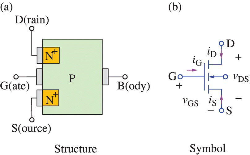
Figure 4.5.2 Structure and symbol of an n‐channel enhancement MOSFET (NMOS).
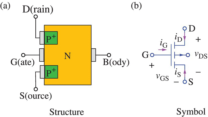
Figure 4.5.3 Structure and symbol of a p‐channel enhancement MOSFET (PMOS).
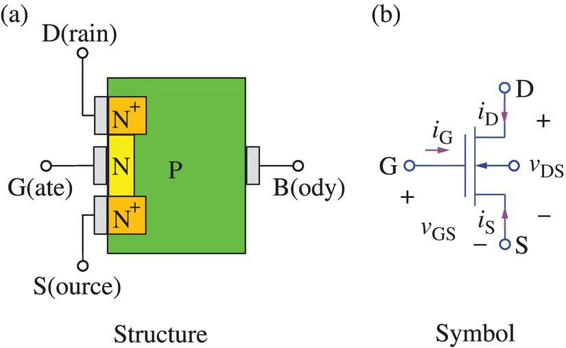
Figure 4.5.4 Structure and symbol of an n‐channel depletion MOSFET (d‐NMOS).
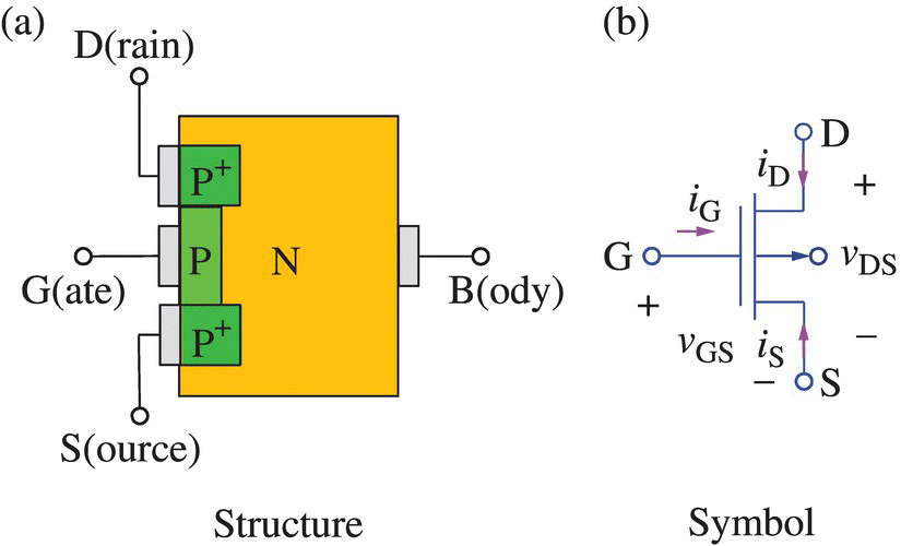
Figure 4.5.5 Structure and symbol of a p‐channel depletion MOSFET (d‐PMOS).
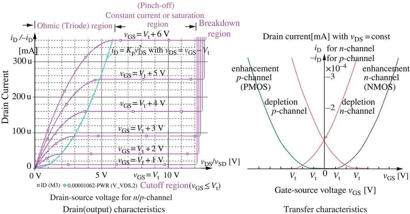
Figure 4.6 Typical characteristics of a MOSFET.
As depicted in Figure 4.6(a), there are three regions (operation modes) besides the breakdown region. Since the operational characteristics of depletion‐type MOSFETs (d‐MOSFETs) are the same with JFETs, we are going to look over the characteristics of enhancement‐mode MOSFETs (e‐MOSFETs) only:
- Ohmic (Triode) region
When 0 < vDS ≤ vGS
−Vt with |Vt| < |vGS| (for an NMOS), the drain current is determined aswhere Kp[A/V2]: conduction parameter or transconductance coefficient, μn[m2/V/s]: mobility of electrons or positive holes in the channel, COX [F/m2]: gate‐to‐channel capacitance per unit area due to the gate oxide, L/W: aspect ratio with length L and width W of the channel, λ [V
‐1]: channel length modulation (CLM) parameter - Saturation (Pinch‐off) or Constant current region
When 0 ≤ vGS
‐Vt ≤ vDS < Vbreakdown (for an NMOS), the drain current is determined asThe boundary between the ohmic and saturation regions (with vDS = vGS
‐Vt) is described by - Cutoff region
If vGS ≤ Vt (for an NMOS) or vGS ≥ Vt (for a PMOS), the MOSFET will be cut off like an open switch.

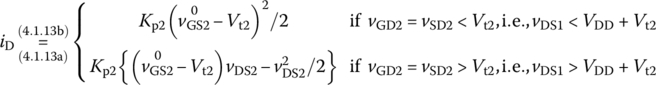
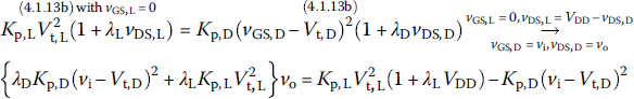
Note that Eqs. (4.1.1) and (4.1.2) and Eqs. (4.1.13a) and (4.1.13b), each describing the i‐v relationships of JFET and MOSFET, are identical except for the definition of the conduction parameter Kp and that is why the above MATLAB function ‘FET_DC_analysis()’ can be used for the DC analysis of FET circuits whether the FET is a JFET or a MOSFET.
Table 4.2 summarizes the circuit symbols and i‐v relationships of JFET and MOSFET.
Table 4.2 Circuit symbols and i‐v relationships of JFET and MOSFET.
| FET type | n‐Channel | p‐Channel | ||||
| JFET | Enhancement MOSFET | Depletion MOSFET | JFET | Enhancement MOSFET | Depletion MOSFET | |
| Circuit symbols |  |
 |
 |
 |
 |
 |
| Threshold voltage Vt | − | + | − | + | − | − |
| Conduction constant Kp | Process conduction parameter |
Process conduction parameter |
||||
| Turn‐on condition | vGS > Vt and vDS > 0 | vSG > |Vt| and vSD > 0 | ||||
| Triode region (Ohmic mode) | vGD = vG − vD > Vt > 0 | vDG = vD − vG > |Vt| | ||||
| Saturation region (Pinch‐off mode) | vGD = vG − vD ≤ Vt | vDG = vD − vG ≤ |Vt| | ||||
| iD ≅ Kp(vGS − Vt)2/2 | iD ≅ Kp (vSG − |Vt|)2/2(4.1.13b) | |||||
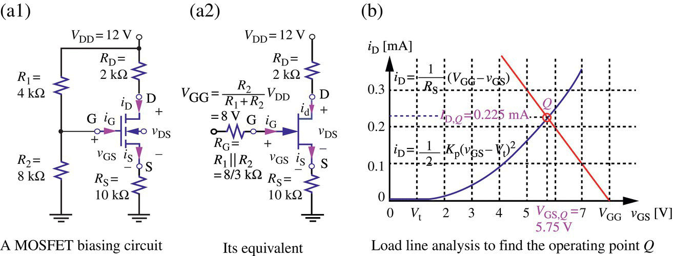
Figure 4.7 DC analysis of a MOSFET circuit.
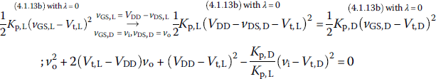
Let us consider the standard FET biasing circuit of Figure 4.7(a1) where the NMOS is biased by the voltage divider consisting of VDD‐R1‐R2. To analyze the circuit, we replace the voltage divider by its Thevenin equivalent as shown in Figure 4.7(a2) and write the following equation by equating the two expressions for the drain current, i.e. one from the KVL equation for the VGG‐GSJ‐RS loop and the other from Eq. (4.1.13b) with λ = 0 as
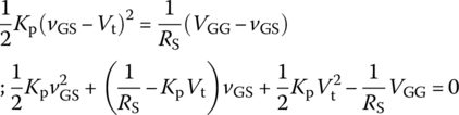
where VDD = 12 V, R1 = 4 kΩ, R2 = 8 kΩ, RD = 2 kΩ, Rs = 10 kΩ, VGG = VDDR2/(R1 + R2) = 8 V, Kp = 2 × 10‐5 A/V2, and Vt = 1 V. We solve this equation to get VGS,Q = 5.75 V and ID,Q = 0.225 mA, which conforms with the operating point Q = (VGS,Q, ID,Q) = (5.75 V, 0.225 mA) obtained from the load line analysis shown in Figure 4.7(b). Then we substitute ID,Q = 0.225 mA for iD into the KVL equation for the D‐S loop to find VDS,Q:
These hand calculations can be done by running the following MATLAB statements:
>>R1=4000; R2=8000; RD=2e3; RS=1e4; VDD=12; Kp=2e-5; Vt=1;FET_DC_analysis(VDD,R1,R2,RD,RS,Kp,Vt);
which yields
VDD VGQ VSQ VDQ IDQ12.00 8.00 2.25 11.55 2.25e-004in the saturation mode with VGD,Q= -3.55[V]<=Vt=1.00
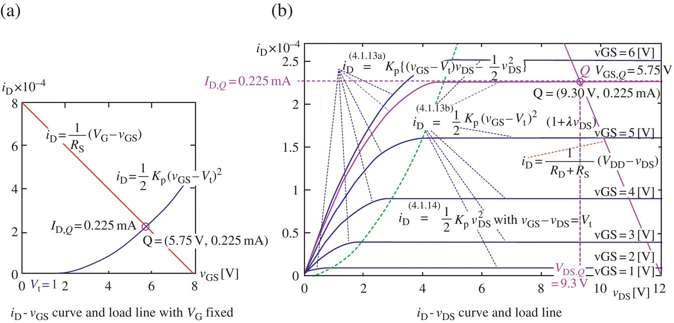
Figure 4.8 Operating point on the iD‐vDS characteristic curve of the NMOS in Figure 4.7(a1).
If you want to locate the operating point Q = (VGS,Q, ID,Q) on the iD‐vDS characteristic curve of the NMOS M1 from the viewpoint of load line analysis, run the following MATLAB script “elec04f08.m” to get Figure 4.8.
These results can be supported by the Bias Point analysis using the PSpice. After running the OrCAD/PSpice project ‘elec04f09.opj’ with the schematic (Figure 4.9(a)), you can click PSpice > View_Output_File on the top menu bar of the Schematic window to see the simulation results shown in Figure 4.9(b). The parameters of PSpice parts MbreakN (enhancement n‐channel)/MbreakND (depletion n‐channel) (referred to as ‘NMOS’/‘NMOS_d’) can be edited as shown in the PSpice Model Editor (Figure 4.9(c1)) opened by selecting the part (to let it pink‐colored) and then clicking Edit > PSpice:Model on the top menu bar of the Schematic window.
Figure 4.9 PSpice simulation for the FET circuit of Figure 4.7(a1) with creating/editing a PSpice model.
Alternatively, you can create a new PSpice model for FET in the following steps:
- Click File > New > PSpice:Library to open the PSpice Model Editor (Figure 4.9(c2)).
- Click Model/New to open the New Model dialog box, set it as Figure 4.9(c2) and click OK to open the model list and parameter list.
- Set the model parameters as Figure 4.9(c3) where most of them are left as their default values.
- Click File/Save to save the created model into a library file in your own directory.
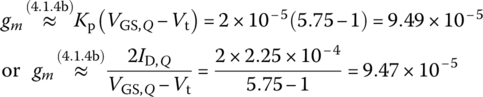
There is one thing to note about the transconductance gain gm, which is one of the AC model parameters for an FET. The PSpice Simulation output file (Figure 4.9(b)) shows that the value of gm(GM) is 9.49 × 10‐5, as can be computed by using Eq. (4.1.4b):
4.1.3 MOSFET Used as a Resistor
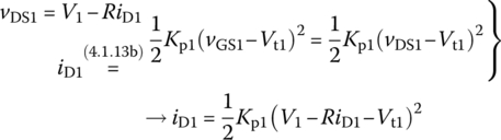
Figure 4.13(a) shows a diode‐connected e‐NMOS with its drain and gate short‐circuited. Its iD‐(vDS=vGS) characteristic can be obtained graphically as the dotted line shown in Figure 4.13(c1) from the locus of points with vDS = vGS and also mathematically by substituting vGS = vDS into Eq. (4.1.13b) (for the saturation mode):
Note that with vDS = vGS, Eq. (4.1.4a) and the reciprocal of Eq. (4.1.4b) conform with each other so that a diode‐connected e‐NMOS can be regarded as just a nonlinear resistor with the small‐signal (incremental or dynamic) resistance
Figure 4.13(a) also shows a diode‐connected d‐NMOS with its source and gate short‐circuited, whose iD‐vDS characteristic can be obtained as the dotted line shown in Figure 4.13(c2) from the locus of points with vGS = 0 where its current is limited unlike an e‐NMOS. These examples imply that a MOSFET can be used as a nonlinear resistor. The theoretical iD‐vDS characteristics of the e‐NMOS/d‐NMOS circuits turn out to agree with the PSpice simulation results shown in Figure 4.13(b).
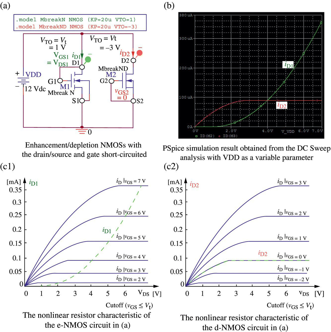
Figure 4.13 Enhancement/depletion type MOSFETs connected as (nonlinear) resistors (“elec04f13.opj”).
4.1.4 FET Current Mirror
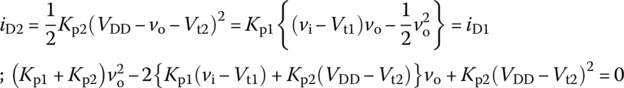
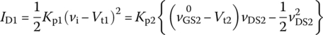
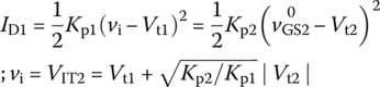
Consider the circuit of Figure 4.14(a) where the FET M1 is said to be ‘diode‐connected’ or ‘connected in diode configuration’ since its source and gate terminals are short‐circuited so that it behaves like a diode. For proper operation of the circuit, the two FETs M1 and M2 must be matched in the sense that they have identical conduction parameters Kp, threshold voltages Vt, and CLM parameters λ. Let us analyze the circuit, which is called a current mirror because the currents of the two matched FETs sharing the same vGS are equal. Noting that since vGD1 = 0 ≤ Vt, M1 (with vGS1 > 0) operates always in the saturation mode, its drain current can be determined by solving
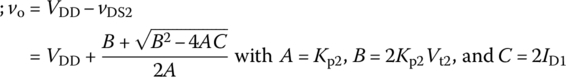
This yields
where A = R2 = 1, B = ‐2{R(V1 − Vt1) + 1/Kp1} = ‐18, and C = (V1 − Vt1)2 = 64. Here, ID1=13.123 mA has been dumped because it does not satisfy even the turn‐on condition vGS1 = V1 − RID1 = 9 − 13.123 > Vt1 = 1[V]. Thus, since vGS1 = vGS2 and Vt1 = Vt2, the output current will be
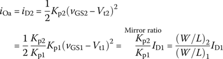
This analysis result conforms with the PSpice simulation result (with DC Sweep analysis) shown in Figure 4.14(d). Note that considering the effect of the CLM parameter, the current transfer ratio or current gain, also called the mirror ratio, can be written as
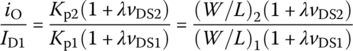
Let us analyze the circuit of Figure 4.14(b) where the three matched FETs have identical threshold voltages Vt and CLM parameters λ, but possibly different conduction parameters {Kp1, Kp2, Kp3}. Since M1 and M3 are diode connected so that vGDk = 0 ≤ Vt for k = 1 and 3, they operate always in the saturation mode (with vGSk > Vt by V1) and thus their drain currents can be expressed as
We can apply KCL at nodes 1 and 2 to write
Once we have solved this set of two nonlinear Eqs. (4.1.24a,b) for v1 and v2 (by using the MATLAB function ‘fsolve()’), we can use Eqs. (4.1.22), (4.1.23), or (4.1.13b) to find the output current iOb = iD2 as long as vGD2 = v1 − V2 < Vt so that M2 is saturated. If vGD2 = v1 − V2 ≥ Vt (so that M2 is in the tride region), Eq. (4.1.13a) should be used to find iOb, as implemented by the MATLAB function ‘iD_NMOS_at_vDS_vGS()’. This solution process for the current mirror of Figure 4.14(b) has been cast into the above MATLAB function ‘FET3_current_mirror()’.
Figure 4.14 Current mirrors using FETs (“elec04f14.opj”).
The two current mirrors of Figure 4.14(a) and (b) have the same output resistance:
Their minimum output voltage, called the compliance voltage, required to keep M2 in saturation is
To use the above function ‘FET3_current_mirror()’ for analyzing the current mirror of Figure 4.14(b), we can run the following statements:
>>Kp=1e-3; Vt=1; lambda=2e-3; R=1e3; V1=9;V2s=[0:0.01:40]; V12=[V1 V2s];[io,ID1,v,Ro,Vomin]= ...FET3_current_mirror(Kp,Vt,lambda,R,V12);plot(V2s,io, Vomin*[1 1],[0 io(end)],'r:')
to get the graph for the output current iOb versus V2 = 0 ~ 40 V like the corresponding PSpice simulation result shown in Figure 4.14(d).
To analyze the current mirror of Figure 4.14(c) with a current source I, we run
>>I=3e-3;[io,ID1,v,Ro,Vomin]= ...FET3_current_mirror(Kp,Vt,lambda,I,V12);plot(V2s,io, Vomin*[1 1],[0 io(end)],'r:')
to get the graph for the output current iOc versus V2 = 0 ~ 40 V like the corresponding PSpice simulation result shown in Figure 4.14(d).
If R = 0, it is not so difficult to derive the analytical expression of v1 even if Kp1≠ Kp3. In this case, we solve Eq. (4.1.25a) for v1 with v2=V1 and Eqs. (4.1.24a,b):
to get
The output current iOb can be determined from Eqs. (4.1.13b) or (4.1.13a) (with vGS = v1 and vDS = V2) depending on whether vGD = v1 −V2 < Vt or vGD = v1 − V2 ≥ Vt so that M2 operates in the saturation or triode region.
- (Q) What advantage does the current mirror of Figure 4.14(b) get from the additional FET M3 over that of Figure 4.14(a)?
- (A) An advantage is a considerable flexibility in the design of current source since Kp3/Kp1 can be fixed at the will of designer by adjusting the width‐to‐length ratios (Wn/Ln) of FETs.
The following MATLAB script “elec04f14.m” can be run to get the plot of the output currents iOa, iOb, and iOc versus V2 = 0 ~ 40 V for the three current mirrors shown in Figure 4.14(a‐c), as depicted in Figure 4.14(d).
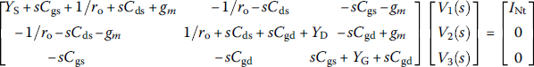
4.1.5 MOSFET Inverter
Just like the BJT inverter of Figure 3.27 introduced in Section 3.1.10, let us consider an FET inverter (shown in Figure 4.16(a)) using an FET/resistor as a driver/load, respectively. To get its voltage transfer characteristic (VTC), suppose that the input voltage vi increases from 0 to VDD. While vi = vGS ≤ Vt, the NMOS is cut off with iD = 0 so that vo = VDD. As vi = vGS > Vt, the NMOS enters the saturation region where the output voltage is determined depending on the input voltage as
When vi = vGS increases over vDS + Vt so that vGD = vGS ‐ vDS > Vt, the NMOS enters the triode region where the input–output relationship is

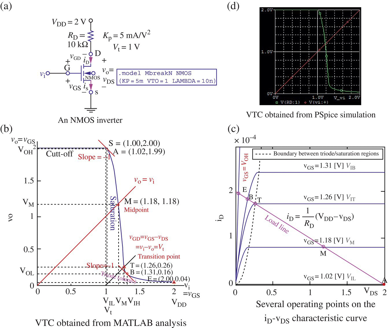
Figure 4.16 An NMOS inverter circuit and its VTC (“elec04f16.opj”).
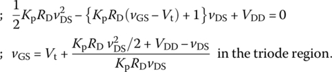
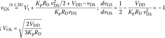
The VTC curve in Figure 4.16(b) is based on these two input–output relationships, each for saturation/triode regions. The transition point T between the saturation and triode segments on the VTC can be determined from vGD = vGS‐ vDS = vi ‐ vo = Vt together with Eq. (4.1.35). That is, we can substitute vGS = Vt + vDS into Eq. (4.1.35) to write
and use the quadratic formula to solve this quadratic equation for the point T = (VIT,VOT) as
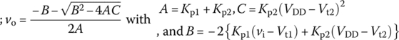
The switching threshold voltage VM, also called the midpoint voltage, can be found by substituting vGS = VM and vDS = VM into the input‐output relationship Eq. (4.1.35) (for the saturation region) and solving it for VM as

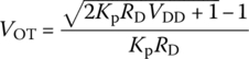
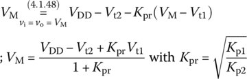
Also, VIL (the maximum input voltage that can be interpreted as “0”) (at point A in Figure 4.16(b)) and the corresponding output voltage VOH (the minimum output voltage that can be interpreted as “1”) can be determined by setting the derivative of Eq. (4.1.35) w.r.t. vGS to ‐1:
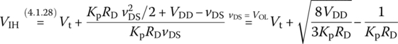
VIH (the minimum input voltage that can be interpreted as “1”) (at point B in Figure 4.16(b)) and the corresponding output voltage VOL (the maximum output voltage that can be interpreted as “0”) can be determined by setting the derivative of Eq. (4.1.37) to ‐1:
Note that the high/low and absolute noise margins are defined by Eqs. (3.1.64) and (3.1.65) as
It may be useful for establishing your overview of the inverter analysis to see that the slope of the VTC (for the saturation region) is ‐KpRD (vGS – Vt) and also that the points A = (VIL,VOH), M = (VM, VM), T = (VIT, VOT), B = (VIH, VOL), and E = (VOH, VOE) on the VTC can be located on the (pink) load line intersecting the corresponding vDS‐iD characteristic curves of the NMOS in Figure 4.16(c).
The above MATLAB function ‘NMOS_inverter()’ uses another function ‘vDS_vGS_ NMOS_inverter()’ (implementing Eqs. (4.1.35) and (4.1.36)) to get the set of output voltage vo of an NMOS inverter for vi = 0 ~ VDD, uses another function ‘find_pars_of_inverter()’ (Section 3.1.10) to find the inverter parameters, and then plots the VTC of the inverter.
4.1.5.1 NMOS Inverter Using an Enhancement NMOS as a Load
Figure 4.17(a) shows an e‐NMOS inverter, that is an NMOS inverter using a diode‐connected enhancement NMOS M2 (with its gate‐drain short‐circuited) as a load resistor where vGD2 = 0 < Vt2 so that M2 is always in saturation with the drain current (common to the two NMOSs):
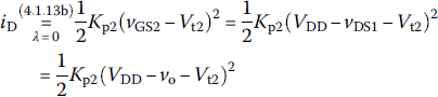
Note that we can write a KVL equation in iD (for path VDD‐DS2‐DS1) or a KCL equation in vDS2 (at node S2‐D1) as
Figure 4.17 An NMOS inverter using an e‐NMOS as a load and its VTC (“elec04f17.opj”).
where the LHS of each equation corresponds to the (nonlinear) load curve (of M2 with Vt2 = 1 [V]), which is plotted as the red line together with the iD‐vDS1 characteristic curves of M1 with Vt1 = 1 [V] in Figure 4.17(b).
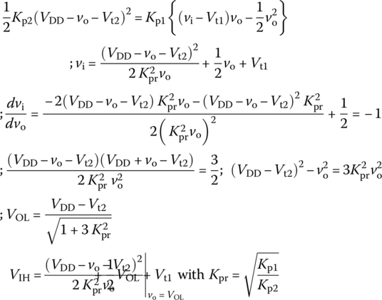
To get its transfer characteristic, suppose that the input voltage vi increases from 0 to VDD. While vi = vGS1 ≤ Vt1, M1 is cut off with iD = 0 so that vo = VDD ‐ vGS2 = VDD‐Vt2 since vGS2 stays at Vt2 as long as iD = 0, as described by point A in the VTC shown in Figure 4.17(c). As vi = vGS > Vt1, M1 enters the saturation region where the drain current can be expressed as
and the output voltage vo can be determined in terms of vi by equating this with Eq. (4.1.45) for iD2:
This linear saturation mode (with slope −Kpr) continues till vo becomes low enough to make vGD1 = vi − vo ≥ Vt1 so that M1 knocks on the door to the triode region, as described by point T:
If vi increases over VIT, M1 enters the triode region where the drain current can be expressed as

and the output voltage vo can be determined in terms of vi by equating Eqs. (4.1.45) and (4.1.51):
Based on these two input‐output relationships (each for the saturation/triode region), we can plot the VTC as depicted in Figure 4.17(c). The VTC can be regarded as having been obtained by taking the values of (vGS1, vDS1) at the operating points, i.e. the intersection points of the load curve of M2 with the drain characteristic curves of M1 for each value of vi = vGS1. Figure 4.17(d) shows the VTC obtained from the PSpice simulation, which is quite similar to that (Figure 4.17(c)) obtained from the theoretical analysis.
The switching threshold voltage VM, also called the midpoint voltage, can be found by substituting vi = VM and vi = VM into the input–output relationship Eq. (4.1.48) (for the saturation region) and solving it for VM as
How about VIL (the maximum input voltage that can be interpreted as “0”) and the corresponding output voltage VOH (the minimum output voltage that can be interpreted as “1”)? Unlike the case of the NMOS inverter with a resistive load, it can't be determined as a point of slope ‐1 because the slope of the VTC abruptly changes from zero to ‐Kpr. Instead, we determine (VIL, VOH) at the turn‐on point A in Figure 4.17(c):
VIH (the minimum input voltage that can be interpreted as “1”) (at point B in Figure 4.17(c)) and the corresponding output voltage VOL (the maximum output voltage that can be interpreted as “0”) can be determined by setting the derivative of dvi/dvo (rather than dvo/dvi for a technical reason) to ‐1:
The processes of using these formulas to find the parameters and plotting the VTC have been cast into the following MATLAB function ‘NMOS2e_inverter()’. To analyze the NMOS inverter of Figure 4.17(a), all you need to do is to run the following MATLAB statements:
>>VDD=6; Vt1=1; Vt2=1; Kp1=1e-3; Kp2=0.1e-3;Kp12=[Kp1 Kp2]; Vt12=[Vt1 Vt2]; NMOS2e_inverter(Kp12,Vt12,VDD);
This will yield the following analysis result and the VTC as depicted in Figure 4.17(c), which conforms with that (in Figure 4.17(d)) obtained from PSpice simulation:
VIL= 1.00, VIH= 2.39, VOL= 0.90, VOH= 5.00, VM= 1.96, VIT= 2.20, VOT= 1.20Noise Margin: NML= 0.10 and NM= 2.61, Average power = 3.330e+00[mW]
4.1.5.2 NMOS Inverter Using a Depletion NMOS as a Load
Figure 4.18(a) shows a d‐NMOS inverter, that is an NMOS inverter using a depletion NMOS M2 (with its gate‐source short‐circuited) as a load resistor where vGS2= 0 > Vt2 so that iD2= iD1= iD is determined by vDS2=VDD‐ vDS1 = VDD‐vo as
The (nonlinear) load curve (of M2 with Vt2= −1 [V]) is plotted as the pink line together with the iD‐vDS1 characteristic curves of M1 with Vt1 = 1 [V] in (b). Note that the load curve and the iD‐vDS1 characteristic curve of M1 for vGS1 = Vt1 ‐ ![]() Vt2 = 2 are symmetric about vDS1 = VDD/2 because they can be switched to each other by substituting vDS2 = VDD
Vt2 = 2 are symmetric about vDS1 = VDD/2 because they can be switched to each other by substituting vDS2 = VDD ‐ vDS1.
To get its transfer characteristic, suppose that the input voltage vi increases from 0 to VDD. While vi = vGS1 ≤ Vt1, M1 is cut off with iD = 0 while M2 is turned on, but with vDS2 = 0 (by Eq. (4.1.57b)) so that vo = VDD ‐ vDS2 = VDD. As vi = vGS1 > Vt1, M2/M1 enter the triode/saturation region where the drain current can be expressed as
and the output voltage vo can be determined in terms of vi by equating this with Eq. (4.1.57b):
From Figure 4.18(b), we can see that during this mode, the operating point moves upward from point S (via point A) along the semiparabolic load curve. When will this mode stop and M2 enter the saturation mode? It is when vGD2 = vSD2 = vDS1‐VDD = Vt2 so that vo = vDS1 = VDD + Vt2 = VOT2. At this point T2, we have
When will this mode stop and M1 enter the triode mode? It is when vGD1 = vGS1 ‐ vDS1 = vi ‐ vo = Vt1. The output voltage vo at this point T can be determined by substituting vi = vo + Vt1 into Eq. (4.1.51) as
Noting that the input voltage vi at this point is the same as VIT (Eq. (4.1.60)) despite the different values of vo, we can see that when vi = VIT, vo may change abruptly between VOT and VOT2 = VDD + Vt2. The midpoint is determined as the constant value of vi along this SAT‐SAT segment:
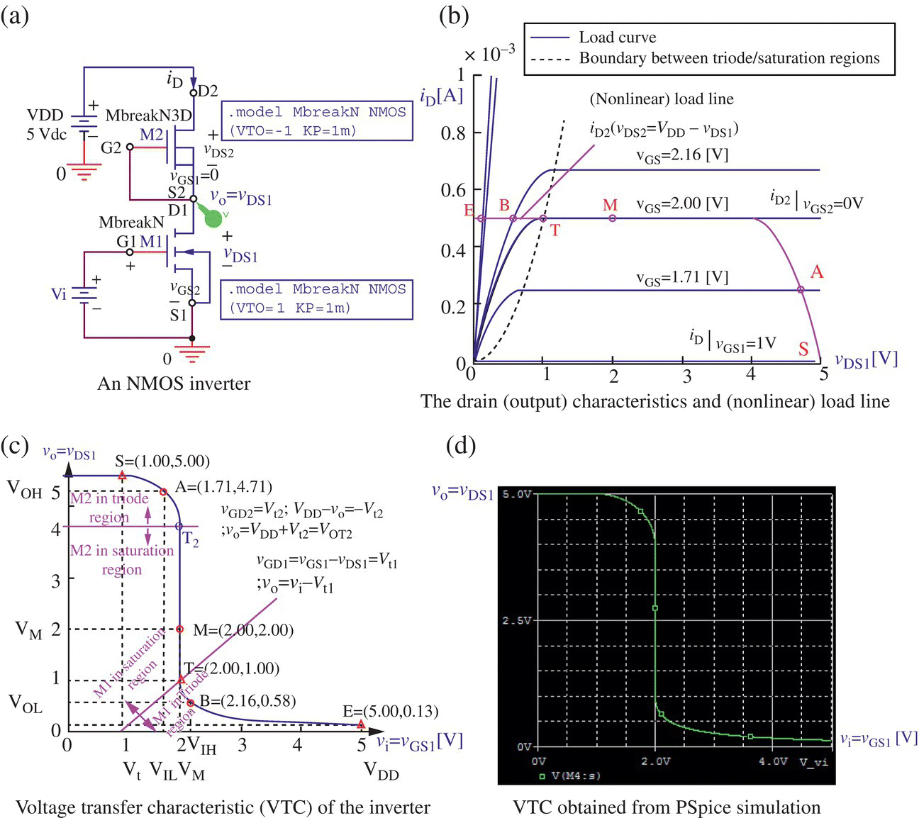
Figure 4.18 An NMOS inverter using a d‐NMOS as a load and its VTC (“elec04f18.opj”).
As vi = vGS1 increases over VIT, M1 enters the triode region while M2 continues to be in saturation so that their drain currents can be expressed as

and the output voltage vo can be determined in terms of vi by equating these two equations:

Based on the two input‐output relationships (Eqs. (4.1.59) and (4.1.63)), we can plot the VTC as depicted in Figure 4.18(c). The process of using these formulas to plot the VTC has been cast into the above MATLAB function ‘NMOS2d_inverter()’, which uses the MATLAB function ‘find_pars_ of_inverter()’ (Section 3.1.10) to find the values of the inverter parameters such as VIL/VOH, VIH/VOL (at the two points with the slope of the VTC equal to ‐1), and VM (at the midpoint).
To analyze the NMOS inverter of Figure 4.18(a), all you need to do is to run the following MATLAB statements:
>>VDD=5; Vt1=1; Vt2=-1; Kp1=1e-3; Kp2=1e-3;Kp12=[Kp1 Kp2]; Vt12=[Vt1 Vt2]; NMOS2d_inverter(Kp12,Vt12,VDD);
This will yield the following analysis result and the VTC as depicted in Figure 4.18(c), which conforms with that (in Figure 4.18(d)) obtained from PSpice simulation:
VIL= 1.708, VIH= 2.155, VOL= 0.577, VOH= 4.706, VM= 2.000NML= 1.131, NMH= 2.551, VL= 0.127, Pavg= 1.250[mW]
Comparing Figures 4.17(c) and 4.18(c), note that the VTC of a d‐NMOS inverter has a steeper transition region and, accordingly, higher noise margins than an e‐NMOS inverter.
4.1.5.3 CMOS Inverter
Figure 4.19(a) shows a CMOS (Complementary MOSFET) inverter using NMOS and PMOS fabricated on the same chip where both gates/drains are tied to the input/output, respectively, and the sources of Mp(PMOS)/Mn(NMOS) are connected to VDD/GND, respectively. Figure 4.19(b) shows the (blue‐lined) iD‐vDSn characteristic curves of Mn depending on vGSn and the (red‐lined) iD – (vSDp = VDD‐vDSn) characteristic curves of Mp depending on vSGp = VDD ‐ vi. A rough VTC of the inverter can be plotted by connecting the operating points (vSGn = vi, vDSn = vo) {S, A, T2, T1, …}, i.e. the intersection points of the characteristic curve of Mn (for vGSn = 0~1, 1.5, 2, 2.5, 3, 3.5, and 4 ~ 5 V) with that of Mp (for vSGp = VDD‐vi = 5~4, 3.5, 3, 2.5, 2, 1.5, and 1 ~ 0 V), as illustrated in Figure 4.19(b) and (c). Figure 4.19(d) shows the VTC obtained from the PSpice simulation.
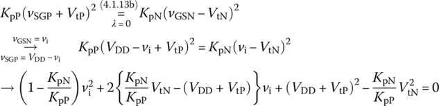
Noting from Figure 4.19(b) and (c) that the operating point moves around the five regions I, II, III, IV, and V as the input voltage vi (applied to the common gate) varies from zero to VDD, let us analyze the inverter to find out the analytical expression of the VTC together with the transition points from a region to another region where the conduction parameters and threshold (turn‐on) voltages of the PMOS/NMOS are KpP/KpN and VtP/VtN, respectively. To this aim, we start from computing the value Vm of the input voltage vi (belonging to region III) at which both Mp and Mn operate in the saturation region by equating the drain currents of Mp and Mn described by Eq. (4.1.13b) (with λ = 0 for simplicity):
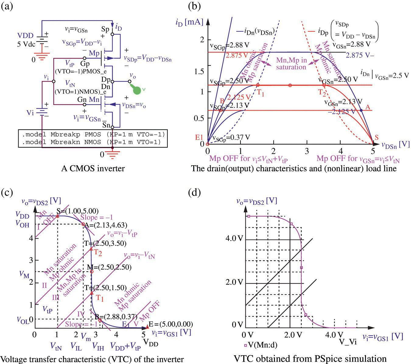
Figure 4.19 A Complementary MOSFET (CMOS) inverter and its voltage transfer characteristic (VTC) (“elec04f19.opj”).

This will be used as the boundary values of vi between regions II and III or III and IV (see Figure 4.19(c)).
<Region I>
When 0 ≤ vi = vGSn ≤ VtN, Mn remains OFF while Mp conducts not in the saturation region but in the ohmic (triode) region because the off‐transistor Mn keeps Mp from conducting as much as it could with vSGp = VDD‐vi ≥ |VtP|. Since the resistance of the off‐transistor Mn is much greater than that of the on‐transistor Mp, almost the whole VDD applies to Mn so that the output voltage is vo ≈ VDD.
<Region II>
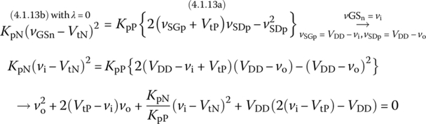
When VtN < vi ≤ Vm, Mn/Mp are assumed to be in the saturation/ohmic regions, respectively (see Figure 4.19(b)) and the operating point is computed by equating the drain currents of Mp and Mn that are described by Eqs. (4.1.13b) (with λ = 0 for simplicity) and (4.1.13a), respectively:
If the (larger) root of this quadratic equation satisfies vo > vi ‐ VtP, the assumption is right. Otherwise, i.e. if
then Mp enters the saturation region and this is region III where both Mp and Mn operate in the saturation mode. The boundary between regions II and III is denoted by the pink line corresponding to vo = vi ‐VtP in Figure 4.19(c).
<Region III>
The inverter stays in Region III (with Mp and Mn saturated) as long as the saturation condition of Mn is satisfied, i.e. if
<Region IV>
If vi increases further enough to break the above condition, i.e. vo < vi ‐VtN, Mn enters the ohmic region (see Figure 4.19(b)) and the operating point is computed by equating the drain currents of Mp (in the saturation region) and Mn (in the ohmic region) that are described by Eqs. (4.1.13b) (with λ = 0 for simplicity) and (4.1.13a), respectively:
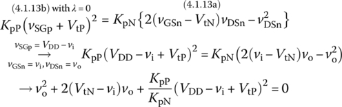
The (smaller) root of this quadratic equation will be vo as long as vi≤ vDD+VtP.
<Region V>
While Mn is still in the ohmic region, Mp will be OFF if
Then almost the whole VDD applies to Mp (with much larger resistance) so that vo ≈ 0.
The process of finding the output voltage of the CMOS inverter to the whole range of the input has been cast into the above MATLAB function ‘CMOS_inverter()’. We have run the above MATLAB script “elec04f19.m” to get not only the following values of the inverter parameters
VIL = 2.1250, VIH = 2.8750, VOL = 0.3750, VOH = 4.6250,VIT2 = 2.5000, VOT2 = 3.5000, Vm = 2.5000, VIT1 = 2.5000, VOT1 = 1.5000,NML = 1.7500, NMH = 1.7500, PDavg = 0.0028
but also the VTC and the drain current of the inverter as depicted in Figures 4.19(c) and 4.20(a), respectively. As can be seen from the VTC in Figure 4.19(c), the lowest/highest output voltage levels are 0/VDD so that the CMOS inverter has the maximum output swing. This, together with the symmetry of the VTC, is the reason why a CMOS inverter can have wide noise margins.
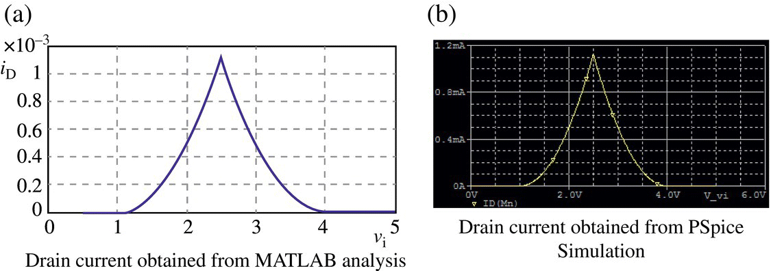
Figure 4.20 Drain currents of the CMOS inverter obtained from MATLAB analysis and PSpice simulation.
Figure 4.20(b) shows the drain current of the inverter obtained from the PSpice simulation, which is quite similar to Figure 4.20(a). What is implied by the current curve(s) in Figure 4.20? The current (drawn from the supply voltage source VDD) is zero when the CMOS inverter is in its output‐high/low state so that the CMOS gate can power down in its static condition, which is one of the major advantages of CMOS configuration.
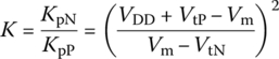
One more thing to note before closing this section is that a formula to determine the geometry ratio K from the given values of VDD, Vm (the boundary value of the input voltage between regions II and III or regions III and IV), VtP (the threshold voltage of PMOS), and VtN (the threshold voltage of NMOS) can be derived from Eq. (4.1.65) as
4.1.6 Source‐Coupled Differential Pair
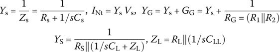
Figure 4.21(a) and (b) shows a source‐coupled (in the sense that the source terminals of the two FETs are connected) or differential (in the sense that its output varies with the differential input vd = vGS1‐vGS2) pair. To analyze this circuit, we assume that the two FETs have identical conduction parameters Kp and threshold voltages Vt, and both of them operate in the saturation mode so that we can use Eq. (4.1.13b) (with λ = 0 for ignoring the CLM effect) to write their approximate drain currents as
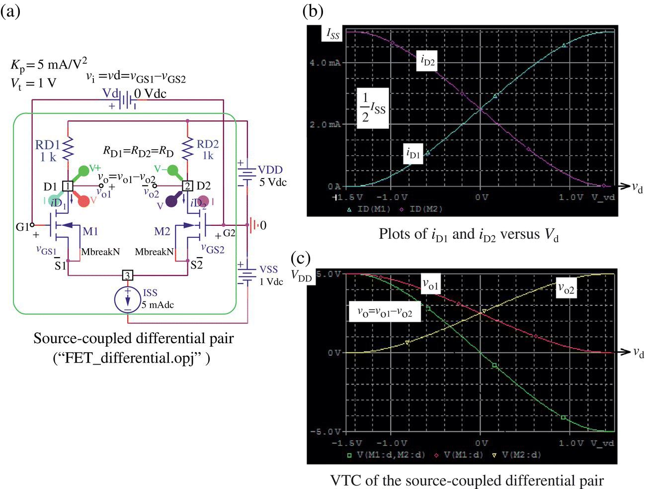
Figure 4.21 Source‐coupled (differential) pair and its VTC.
Thus, the difference between their square roots can be written as
Also, we apply KCL at node 3 (S1‐S2) to write
Subtracting the square of Eq. (4.1.73) from Eq. (4.1.74) yields
Thus, iD1 and iD2 can be found from the two roots of the quadratic equation:
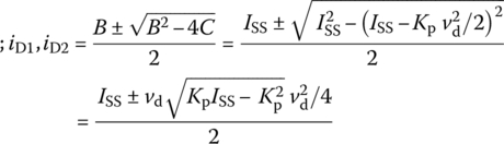
where these drain currents are depicted in Figure 4.21(b). Then we can write the (differential) output voltage as
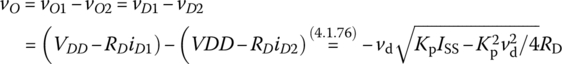
This differential output voltage vo, together with vo1 and vo2, is shown in Figure 4.21(c). From Figure 4.21 and Eqs. (4.1.76) and (4.1.77), note the following:
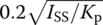
- If |vd| <
 , the differential output voltage vo and other signals vary almost linearly with the differential input vd, allowing the source‐coupled pair to be used as an amplifier with a voltage gain of
(4.1.78)
, the differential output voltage vo and other signals vary almost linearly with the differential input vd, allowing the source‐coupled pair to be used as an amplifier with a voltage gain of
(4.1.78)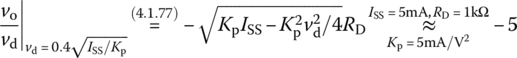
- If vd >
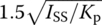 , we have
(4.1.79a)
, we have
(4.1.79a)
On the other hand, if vd < ‐1.5![]() , we have
, we have
It is implied that a large swing of the differential input vd = ±![]() makes the two FETs M1/M2 operate as a closed or an open switch, producing two distinct levels of differential output vo depending on whether vd =
makes the two FETs M1/M2 operate as a closed or an open switch, producing two distinct levels of differential output vo depending on whether vd = ![]() or vd =
or vd = ‐![]() .
.
The small‐signal input‐output relationship of the differential pair can be derived by substituting Eqs. (4.1.72a,b) directly into Eq. (4.1.77):
Note that the differential (mode) voltage gain ‐gmRD can be regarded as the voltage gain (Eq. (4.2.6b)) of a common‐source (CS) amplifier with RS1 = 0 and RL = ∞. Note also that if vo1 or vo2, instead of vo, is taken as the output, the differential voltage gain gmRD is halved:
The amplifying/switching properties are extensively used in analog/digital circuits, respectively. That is why the source‐coupled differential pair is one of the most important configurations employed in ICs.
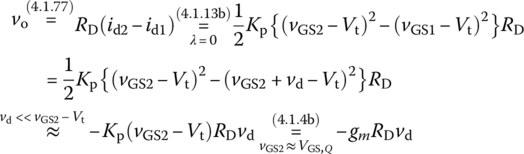
To analyze the FET differential pair circuit in Figure 4.21(a), we can apply KCL at nodes 1, 2, and 3 to write
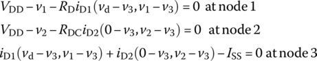
where iDk (vGSk, vDSk) is defined by Eqs. (4.1.13a,b) as
The process of solving this set of equations to find v = [v1 v2 v3] for vd = ‐Vdm~ + Vdm and plotting vo = v1‐v2, iD1, iD2 (together with their analytic values computed by Eqs. (4.1.79) and (4.1.83)) versus vd has been cast into the following MATLAB function ‘FET_differential()’. We can run
>>Kp=5e-3; Vt=1; lambda=0; ISS=5e-3; RD=1e3; VDD=5; Vdm=1.5;dvd=Vdm/1000;vds=[-Vdm:dvd:Vdm];FET_differential(Kp,Vt,lambda,ISS,RD,VDD,vds);
to get the graphs of iD1, iD2, and vo as depicted in Figure 4.21(b) and (c).
4.1.7 CMOS Logic Circuits
Figure 4.22(a)‐(c) shows a two‐input CMOS NOR gate, a two‐input CMOS NAND gate, and a CMOS (bidirectional) transmission gate together with their truth tables where the substrates of the PMOS(Mp) and NMOS(Mn) are connected to the most positive/negative potentials (that are VDD/GND), respectively. The transmission gate makes possible the tristate output or wired‐or connection in CMOS circuits and can be used as building blocks for logic circuitry such as a D flip‐flop. Figure 4.23 shows a 256 × 8 bit (256 bytes) NMOS ROM chip where each one of the 256 bytes stored in the memory can be selected by the word line, which is set to High depending on the 8‐bit address code input to the 8‐input 128‐output decoder.
Here are some comparisons of CMOS and NMOS gates:
- CMOS gates have extremely high input impedance, but they are susceptible to damage.
- CMOS gates consume very little power.
- CMOS gates can achieve noise immunity amounting to 45% of the full logic swing.
- Since a CMOS gate requires more transistors than an NMOS gate having the same logic function, not only its size but also its capacitance is larger.
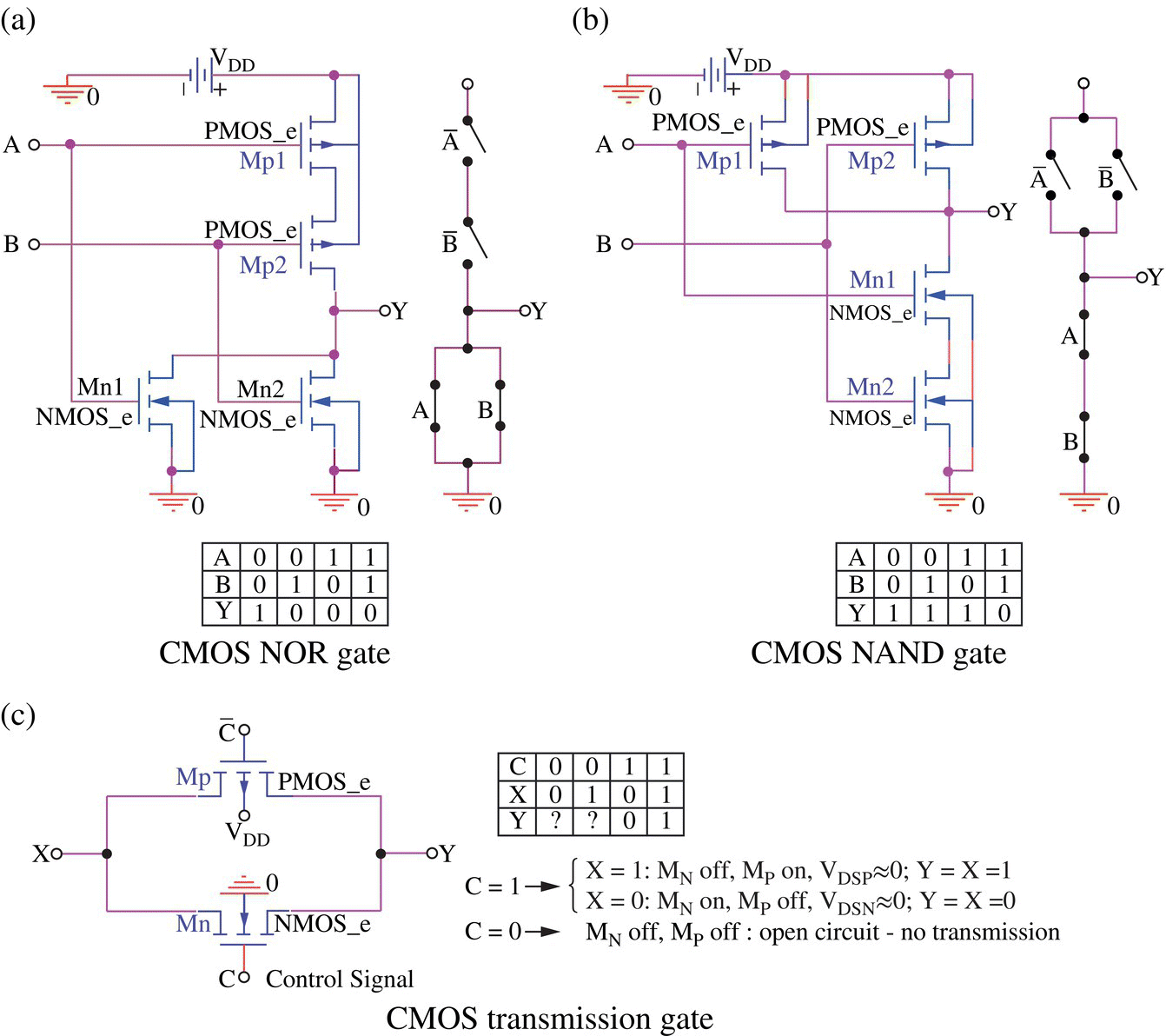
Figure 4.22 Various CMOS logic circuits.
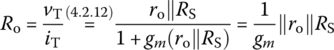
4.2 FET Amplifer
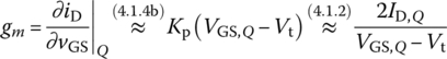
If an FET is used for the purpose of small‐signal amplification, it is supposed to be operating in the saturation region (for the range of input signal vGS = VGS,Q + vgs around VGS,Q at the bias point Q) where its drain current is expressed by
and additionally, its small‐signal component id can be approximated linearly in terms of vgs:

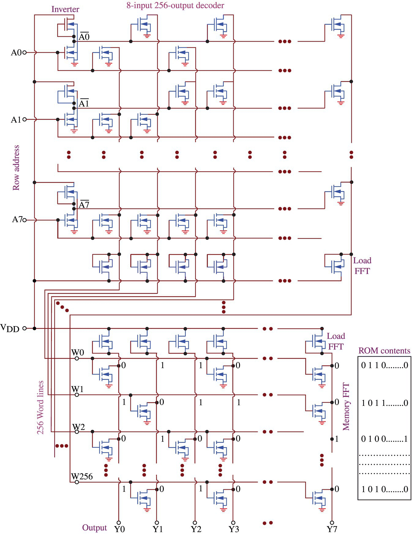
Figure 4.23 256 × 8 bit (256 bytes) NMOS ROM chip.
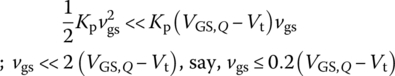
In order for this linear approximation to be valid, the last term of degree 2 must be negligibly small:
so that
This section deals with three configurations of FET amplifier, i.e. the CS (common‐source) amplifier, the CD (common‐drain) amplifier (called a source follower), and the CG (common‐gate) amplifier.
4.2.1 Common‐Source (CS) Amplifier
Figure 4.24 shows a CS FET amplifier and its low‐frequency AC equivalent where the FET has been replaced by the equivalent in Figure 4.3(b). Let us find the input resistance, voltage gain, and output resistance. The formulas have been implemented in the MATLAB function ‘FET_CS_analysis()’.
- Input Resistance Ri
Since the gate current of the FET is almost zero, the equivalent resistance seen from the input side (see Figure 4.24(b1)) is
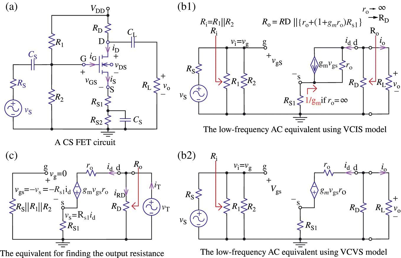
Figure 4.24 A CS (common‐source) FET circuit and its low‐frequency AC equivalent.
- Voltage Gains Gvand Av
To find the voltage gain, we write the node equation for the circuit of Figure 4.24(b1) as

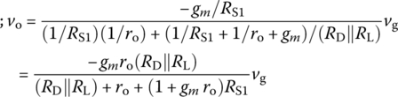
Noting that vi = vg = Ri vs/(Rs + Ri), we can write the voltage gains, i.e. the ratios of the output voltage vo to the source voltage vs and the input voltage vi as
(4.2.6a)
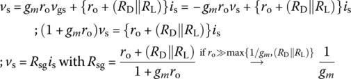
- Output Resistance Ro
To find the (Thevenin) equivalent resistance seen from the load side, we need to remove the (independent) voltage source vs by short‐circuiting it as depicted in Figure 4.24(c). Then, with the test voltage vT applied across RD, we write the drain current id as
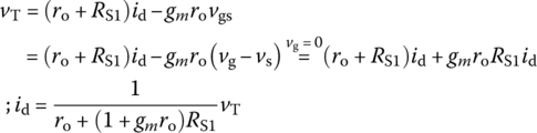
Since the test current iT flowing out of vT is the sum of id and
 :
: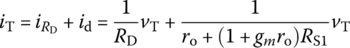
Therefore, the output resistance turns out to be
- Maximum Small‐Signal Input vs,maxfor Linear Amplification
Noting that if ro is very large in Figure 4.24(b1),
(4.2.8)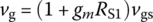
the maximum small‐signal input satisfying the condition (4.2.3) for linear amplification can be determined as

4.2.2 CD Amplifier (Source Follower)
Figure 4.26 shows a CD FET amplifier and its low‐frequency AC equivalent where the FET has been replaced by the equivalent in Figure 4.3(b). Let us find the input resistance, voltage gain, and output resistance. The formulas have been implemented in the MATLAB function ‘FET_CD_analysis()’.
- Input Resistance Ri
Since the gate current of the FET is almost zero, the input resistance is
- Voltage Gains Gvand Av
To find the voltage gain Av = vo /vi, we write the node equation for the circuit of Figure 4.26(b1) as
Thus, we have the voltage gains as
This implies that if Rs ≪ Ri and gm (ro||Rs||RL) ≫ 1, the output voltage is almost equal to the input and source voltages and that is why the CD amplifier is called a voltage follower.
- Output Resistance Ro
To find the output resistance, we remove the (independent) voltage source, vi, by short‐circuiting it as depicted in Figure 4.26(c). Then, with the test current iT applied to the output port, we can get
- Maximum Small‐Signal Input vs,maxfor Linear Amplification
Noting that if ro is very large in Figure 4.26(b1),

Figure 4.26 A CD (common‐drain) FET circuit and its low‐frequency AC equivalent.
we can write the maximum small‐signal input satisfying the condition (4.2.3) for linear amplification as

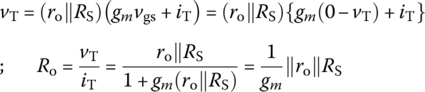
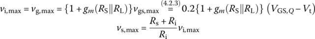
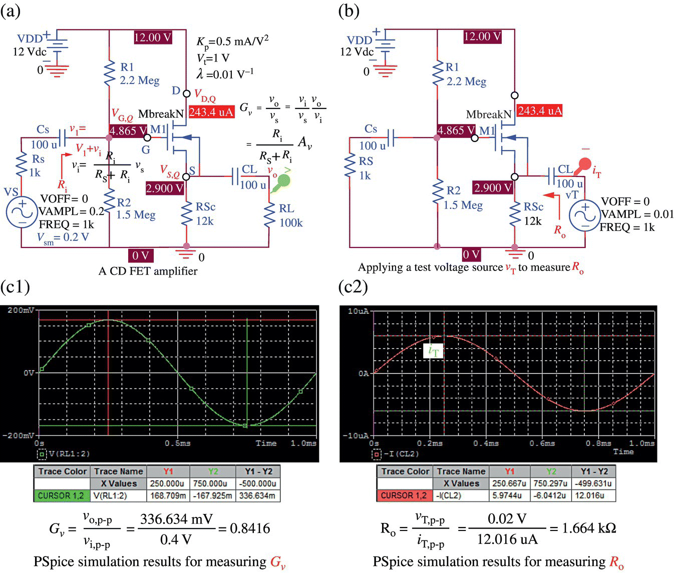
Figure 4.27 A CD FET amplifier and its PSpice simulation results (“elec04e07.opj”).
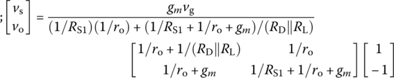
4.2.3 Common‐Gate (CG) Amplifier
Figure 4.28 shows a CG amplifier and its low‐frequency AC equivalent where the FET has been replaced by the equivalent in Figure 4.3(b). Let us find the input resistance, voltage gain, and output resistance. The formulas have been implemented in the MATLAB function ‘FET_CG_analysis()’.
- Input Resistance Ri
To find the input resistance, we apply a test voltage source vs between node s and GND (as depicted in Figure 4.28(c)) and then write the relationship of vs and is as
This implies that the equivalent resistance of the FET between node s and GND is Rsg. Thus, the input resistance is the parallel combination of RS and Rsg:
Figure 4.28 A CG (common‐gate) FET circuit and its low‐frequency AC equivalent.
- Voltage Gains Gvand Av
Since (during the process of computing Ri) the current through RD||RL caused by vs was found to be
the output voltage (across RD||RL) can be expressed as
Thus, taking account of vi = Ri vsig/(Rs + Ri), we can write the voltage gains, i.e. the ratios of the output voltage vo to the source voltage vsig and the input voltage vi as
- Output Resistance Ro
To find the output resistance, we remove the (independent) voltage source vi by short‐circuiting it. Then, we can write the output resistance as
- Maximum Small‐Signal Input vs,maxfor Linear Amplification
Since |vi| = |vg| = |vgs|, the maximum small‐signal input satisfying the condition (4.2.3) for linear amplification can be determined as
4.2.4 Common‐Source (CS) Amplifier with FET Load
4.2.4.1 CS Amplifier with an Enhancement FET Load
Figure 4.30(a) shows a CS amplifier with an enhancement NMOS driver MD and an enhancement NMOS load ML, which is diode connected with its gate and drain short‐circuited so that it can act like a nonlinear resistor. The drain (output) characteristic curves of MD (for several values of vGS) are plotted as solid lines while the iD,L−vDS,L and iD,L−vDS,D=VDD−vDS,L relationships of ML (with vGS,L = vDS,L) are plotted as the lines of square/circle symbols, respectively, in Figure 4.30(b) where the conduction parameter Kp, threshold voltage Vt, and CLM parameter λ of MD and ML are
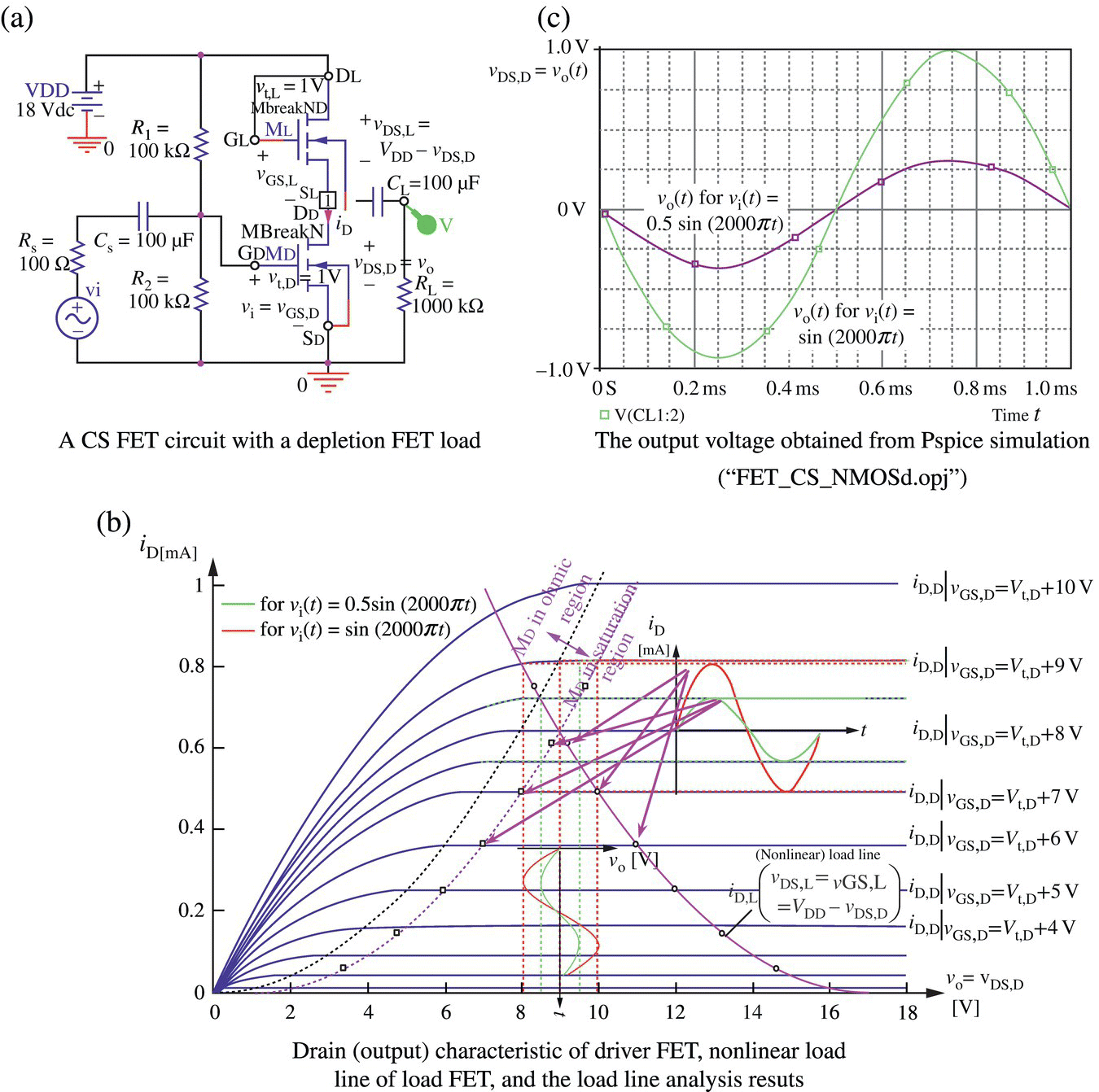
Figure 4.30 A CS amplifier with an enhancement FET load, its load line analysis, and PSpice simulation results.
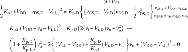
From the locus of dynamic operating points obtained from the intersections of the (pink solid) load line and the characteristic curves of MD (for several values of vi = vGS,D), the graphs of iD(t) = iD,L(t) = iD,D(t) and vo(t) = vDS,D(t) for the sinusoidal input vi(t) = Vsm sin (2000πt) (with Vsm = 0.5 or 1) applied to the G‐S terminals of MD have been plotted as the green and red lines in Figure 4.30(b).
Note that the intersection of the load line of ML and the characteristic curve of MD for a certain value of the input vGS,D = vi (>Vt,D) can analytically be obtained as follows:
- (Step 1) Assuming that both NMOSs are in the saturation region, we find the smaller one of the two roots of the following quadratic equation since the larger one (>VDD) must be invalid:
- (Step 2) If this (tentative) solution is not in the saturation region of MD, i.e. vDS,D < vGS,D
‐Vt,D so that vGD,D = vGS,D‐vDS,D >Vt,D, we assume that MD is in the ohmic region and find the smaller one of the two roots of the following quadratic equation:
This process of analyzing the CS amplifier with an enhanced FET load has been cast into the above MATLAB function ‘FET_CS_NMOSe()’. We can run the following MATLAB script “do_FET_CS_NMOSe.m” to plot the output vo(t) to the input vi(t) = 0.5 sin (2000πt) for t = 0 ~ 1 ms like the PSpice simulation result shown in Figure 4.30(c).
CS Amplifier with a Depletion FET Load
Figure 4.31(a) shows a CS amplifier with an enhancement NMOS driver MD and a depletion NMOS load ML, which is diode connected with its gate and source short‐circuited so that it can act like a current‐limited nonlinear resistor. The drain (output) characteristic curves of MD (for several values of vGS) are plotted as blue lines while the iD,L – vDS,L and iD,L – vDS,D = VDD – vDS,L relationships of ML (with vGS,L = 0) are plotted as the lines of square/circle symbols, respectively, in Figure 4.31(b) where the conduction parameter Kp, threshold voltage Vt, and CLM parameter λ of MD and ML are
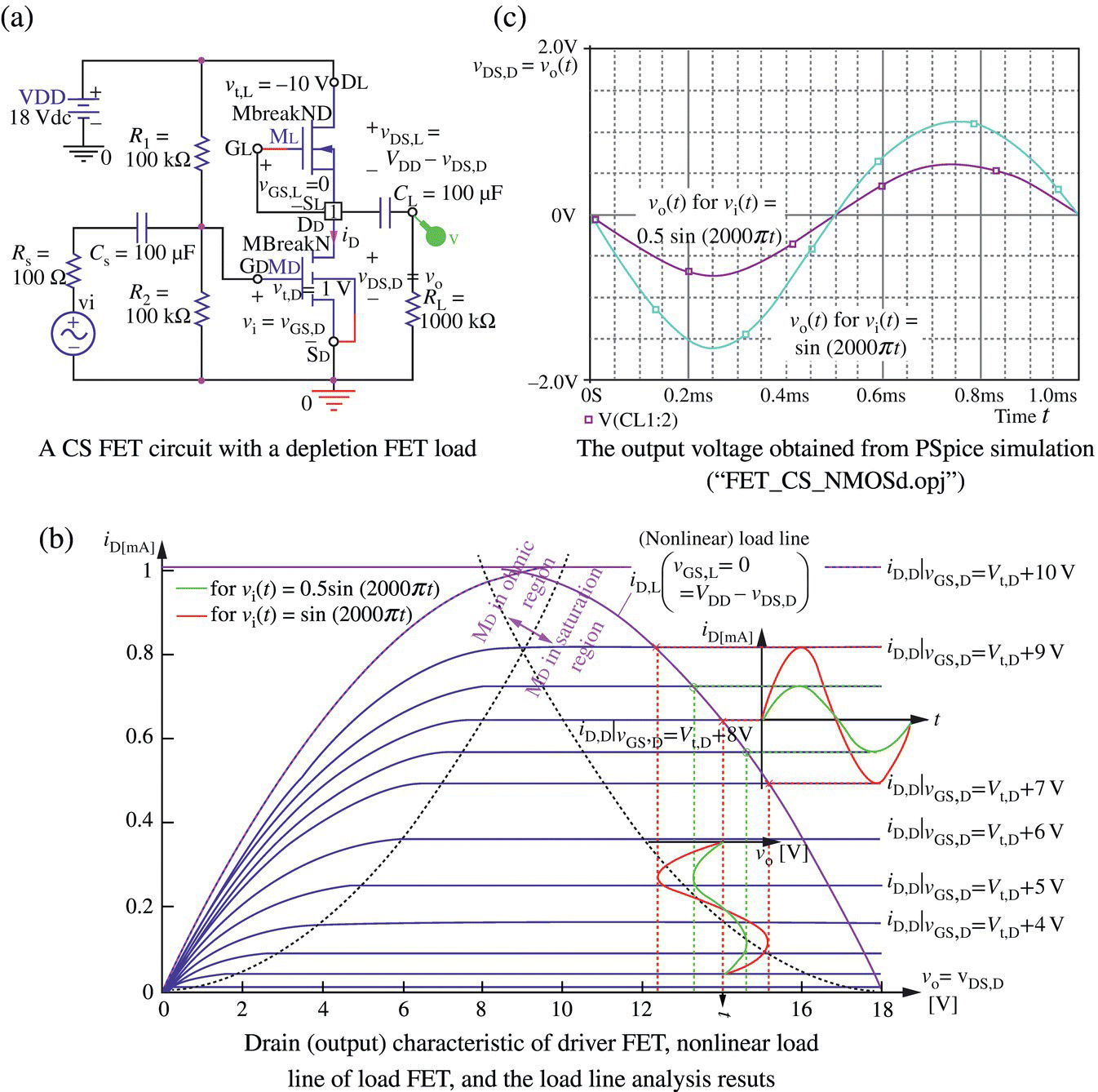
Figure 4.31 A CS amplifier with a depletion FET load, its load line analysis, and PSpice simulation results.
From the locus of dynamic operating points obtained from the intersections of the (pink solid) load line and the characteristic curves of MD (for several values of vi = vGS), the graphs of iD(t) = iD,L(t) = iD,D(t) and vo(t) = vDS,D(t) for the sinusoidal input vi(t) = Vsm sin (2000πt) (with Vsm = 0.5 or 1) applied to the G‐S terminals of MD can be plotted as the green and red lines, respectively, in Figure 4.31(b).
Note that the intersection of the load line of ML and the characteristic curve of MD for a certain value of the input vGS,D = vi (>Vt,D) can analytically be found as follows:
- (Step 1) Assuming that both NMOSs are in the saturation region, find the root of the following first‐degree polynomial equation:
- (Step 2) If this tentative solution is in the ohmic region of MD, i.e. vo = vDS,D < vGS,D − Vt,D = vi − Vt,D, the following equation should be solved on the assumption that MD is in the ohmic region: where the smaller one of the two roots should be taken as vo,Q = VDS,D because the larger one must be invalid.
- (Step 3) If the tentative solution is in the ohmic region of ML, i.e. vo = vDS,D > VDD + Vt,L so that vGD,L =
‐vDS,L =‐(VDD − vDS,D) > Vt,L, the following equation should be solved on the assumption that ML is in the ohmic region: where the larger one of the two roots should be taken as the value of vo because the smaller one must be invalid.
This process of analyzing the CS amplifier with a depletion FET load has been cast into the above MATLAB function ‘FET_CS_NMOSd()’.
An alternative to analyze the circuit of Figure 4.31(a) is to solve the KCL at node 1:
where vGS,D = VGSQ,D + vi with VGSQ,D = VDDR2/(R1 + R2) and iDk(vGSk, vDSk) is defined as Eq. (4.1.83). This algorithm can be implemented by replacing the for loop of the above MATLAB function ‘FET_CS_NMOSd()’ by the following block of statements:
Isn't it interesting that this simple algorithm of solving just one (seemingly nonlinear) equation can replace the above individual quadratic equation approach?
We can run the following MATLAB script “do_FET_CS_NMOSd.m” to plot the output vo(t) to the input vi(t) = 0.5 sin (2000πt) for t = 0 ~ 1 ms like the PSpice simulation result shown in Figure 4.31(c).
4.2.5 Multistage FET Amplifiers
Table 4.3 lists the formulas for finding the input/output resistances, voltage gain, and maximum small‐signal input (for linear amplification) of the CS/CD/CG amplifiers. It also shows the conditions to be met by the coupling/bypass capacitors, whose AC impedances have been assumed to be negligibly small (for a frequency range of interest) compared with the equivalent impedance seen from their two terminals for AC analysis (see Section 14.7 of [J-1]).Note that finding the input/output resistance of a CG configuration requires the input/output resistance of the next/previous stage corresponding to its load/source resistance RL/Rs as implied by Eqs. (4.2.15) and (4.2.17). That is why, for a systematic analysis of a multistage amplifier containing one or more CG configurations, we should find the input/output resistance of each stage, starting from the last/first stage backwards/forwards to the first/last stage where to the last/first stage, the input/output resistance of the next/previous stage is nothing but the load/source resistance.
Each of the formulas listed in Table 4.3 has been coded in MATLAB as follows so that they can be called individually as symbolic expressions whenever and wherever needed. For instance, the formula for the voltage gain Av can be recalled by typing ‘Av_CS’ at the MATLAB prompt.
Table 4.3 Characteristics of CS/CD/CG amplifiers.

4.3 Design of FET Amplifier
4.3.1 Design of CS Amplifier
This section will show how a CS amplifier (illustrated in Figure 4.37) can be designed to achieve a desired voltage gain Av,d and a desired input resistance Ri,d, i.e. how the values of resistors constituting the circuit can be determined to make the voltage gain and input resistance as desired.
As with the CE amplifier discussed in Section 3.4.1, to maximize the AC swing of output voltage vo along the AC load line, it may be good to set the drain current ID,Q and drain‐to‐source voltage VDS,Q of FET at the operating point Q as half the maximum drain current and about one‐third of VDD, respectively:
The gate‐to‐source voltage VGS,Q at the operating point can be found from Eq. (4.1.2) or (4.1.13b) with λ = 0 as
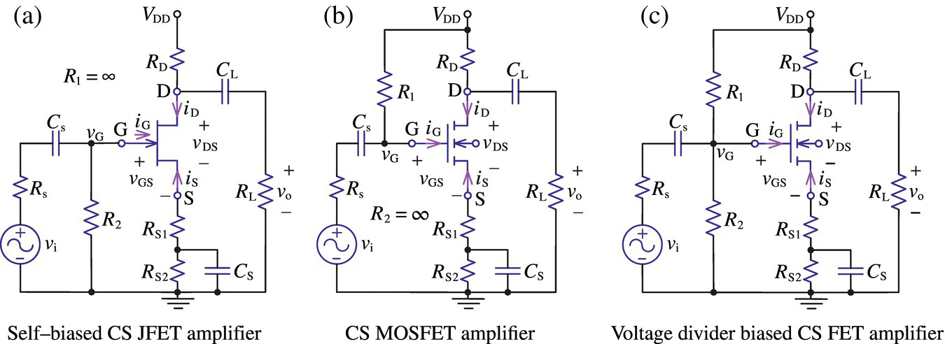
Figure 4.37 CS (common‐source) FET amplifiers.
Then, RD and RS are determined in different ways depending on whether the biasing circuit consists of one resistor (R2 or R1 as shown in Figure 4.37(a) or (b)) or two resistors R1‐R2 (constituting a voltage divider as shown in Figure 4.37(c)):
Note that the minimum power ratings of R1, R2, RC, RS1, and RS2 should be
This process of designing a CS amplifier with a specified voltage gain Av,d and a desired input resistance Ri,d has been cast into the above MATLAB function ‘FET_CS_design()’ where the default value of design constant KC is 1/3.
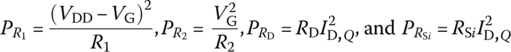
Let us use the MATLAB function ‘FET_CS_design()’ to design the four‐resistor biasing network for a CS amplifier using an NMOS IRF150 so that it can operate with a desired voltage gain Av,d = −20 (for a load resistance of RL = 50 kΩ) and an input resistance Ri,d=100 kΩ at an operating point Q=(VDS,Q, ID,Q)= (VDD/3,0.3 mA) where the device parameters of the FET are Kp = 3.08 A/V2 and Vt = 2.831 V and a VDD = 18 V‐source is available for biasing the FET. To this end, we run the following script “design_CS_IRF150.m”:
This yields
>>design_CS_IRF150Design ResultsR1 R2 RD RS1 RS2 Avd371520 136830 33333 977 5690 20.00Analysis ResultsVDD VGQ VSQ VDQ IDQ18.00 4.84 2.00 8.00 3.00e-004in the saturation mode with VGD,Q= -3.15[V] (Vt=2.83)gm= 43.948[mS], ro= 464.368[kOhm]Ri= 100.00 kOhm, Ro= 33279 OhmGv=Ri/(Rs+Ri)xAvoxRL/(Ro+RL) = 0.9995x(-33.30x0.6004=-19.99) = -19.98
Here, from the PSpice model opened by selecting the part IRF150 and clicking Edit > PSpice:Model from the top menu bar of the PSpice Schematic window or from the PSpice simulation output file (Figure 4.38(b)), we see KP = 20.53E−06, L = 2E−06, W = 0.3, Vto = 2.831, and RDS = 444.4E+03, which can be interpreted as meaning
The above results mean the following values of the resistances of designed CS amplifier:
The script uses ‘FET_CS_analysis()’ (Section 4.2.1) for analyzing the designed circuit to get the DC analysis result:
and the AC analysis result: Gv = −19.98, Ri = 100 kΩ, and Ro = 33.3 kΩ.
Figure 4.38(a) and (b) shows the PSpice schematic of the designed CS amplifier and its simulation results where the overall voltage gain has turned out to be Gv,PSpice = −1.9887/99.725 m ≈ −19.94 as required by the design specification. It is implied that the MATLAB design and analysis functions have worked well.
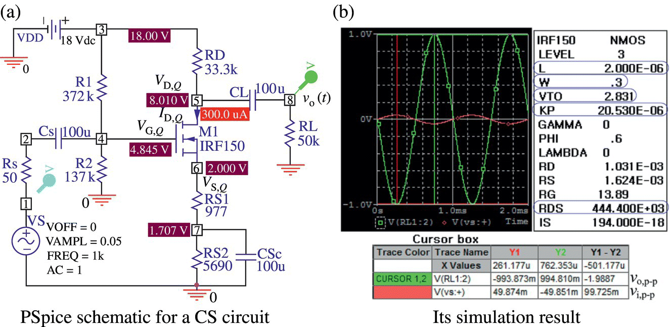
Figure 4.38 A CS (common‐source) circuit and its PSpice simulation (“elec04f38.opj”).
4.3.2 Design of CD Amplifier
This section will show how a CD amplifier with RD = 0 (as shown in Figure 4.40) can be designed to achieve a desired input resistance Ri,d, i.e. how the values of resistors constituting the circuit can be determined to yield a desired input resistance.
Figure 4.40 A CD (common‐drain) FET circuit and its low‐frequency AC equivalent.
As with the CS amplifier discussed in Section 4.3.1, to maximize the AC swing of output voltage vo along the AC load line, it may be good to set the draincurrent ID,Q and drain‐to‐source voltage VDS,Q of FET at the operating point Q as half the maximum drain current and about one‐third of VDD, respectively:
The source resistance RS can be determined as
Also, the gate‐to‐source voltage VGS,Q at the operating point can be determined from Eq. (4.1.1b) or (4.1.13b) as
Then, the node voltage VG,Q at the gate terminal can be obtained as
If VG,Q ≤ VDD, the values of resistors R1 and R2 can be determined so that their parallel combination equals the desired input resistance Ri,d:
Otherwise, i.e. if VG,Q > VDD (which is impossible), we set VG,Q = VDD and
If you want to find the new operating point, the KCL equation at node S,
should be solved for vS, yielding VS,Q and consequently,
Now, suppose the resulting voltage gain Av turns out to be intolerably smaller than 1 and/or the resulting output resistance Ro is quite larger than you expected. Should we increase or decrease the drain current ID,Q to improve the values of Av and Ro? To find the answer to this question, let us recollect the formulas for determining Av and Ro of a CD amplifier:

Noting from Eqs. (4.3.19)?> and (4.3.28) that as ID,Q increases, RS decreases, and gm increases, we can tell that a larger value of ID,Q will help to increase Av (Eq. (4.3.26)) and decrease Ro (Eq. (4.3.27)).
The above process of designing a CD amplifier with a desired input resistance Ri,d has been cast into the following MATLAB function ‘FET_CD_design()’.
4.4 FET Amplifier Frequency Response
In this section, we will find the transfer function G(s) = Vo(s)/Vi(s) and frequency response G(jω) for a CS amplifier, a CD amplifier, and a CG amplifier with the FET replaced by the high‐frequency small‐signal model shown in Figure 4.3(a).
4.4.1 CS Amplifier
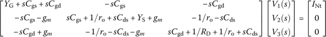
Figure 4.42(a) and (b) shows a CS amplifier circuit and its high‐frequency small‐signal equivalent, respectively, where one more load capacitor CLL, in addition to the output capacitor CL, is connected in parallel with the load resistor RL. For the equivalent circuit shown in Figure 4.42(b), a set of three node equations in V1 = Vg, V2 = Vd, and V3 = Vs can be set up as
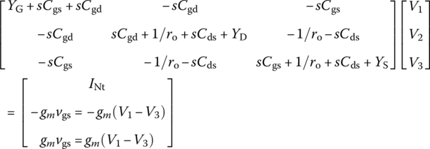
where


Figure 4.42 A CS (common‐source) FET circuit and its high‐frequency AC equivalent.
- (Q) How about if RS1 + RS2 = 0 ?
Here, INt and YB are the values of Norton current source and admittance looking back into the source part from terminals g to 0. This equation can be rearranged into a solvable form with all the unknown/known terms on the LHS/RHS as
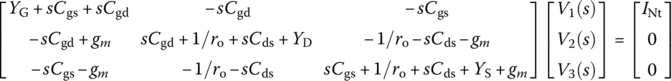
and solved for V1, V2, and V3. Then, the transfer function and frequency response can be found:

This process to find the transfer function and frequency response has been cast into the following MATLAB function ‘FET_CS_xfer_ftn()’.
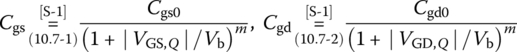
Note the following about the internal capacitances of an FET, i.e. the gate‐to‐source capacitance Cgs, the gate‐to‐drain capacitance (sometimes called the overlap capacitance) Cgd, and the drain‐to‐source capacitance Cds ([S-1]):
- Cds can usually be ignored since Cds≪Cgs. Cgs and Cgd can be modeled as voltage‐dependent capacitances with values determined by
where Cgs0/Cgd0[F]: zero‐bias gate‐source/gate‐drain junction capacitances, respectively, VGS,Q/VGD,Q[V]: quiescent gate‐source/gate‐drain voltages, respectively, m(Mj): gate p‐n grading coefficient (SPICE default = 0.5), and Vb(Pb): gate junction (barrier) potential, typically 0.6 V (SPICE default = 1 V).
- The zero bias capacitances have dimensions of [F/m]/[F] for MOSFET/JFET, respectively.
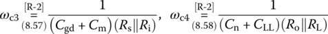
Referring to Figure 4.43, four break (pole or corner) frequencies determining roughly the frequency response magnitude can be determined as [R-2]
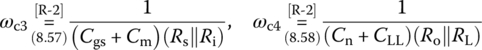
Note the following about these four break frequencies:
- ωC1, related with the coupling capacitor Cs, is obtained as the reciprocal of the product of Cs and the equivalent resistance as seen from Cs (Figure 4.43(a)).

Figure 4.43 (Approximate) equivalent circuits for finding the equivalent resistance seen from each capacitor.
- ωC2, related with the output capacitor CL, is obtained as the reciprocal of the product of CL and the equivalent resistance as seen from CL (Figure 4.43(c)).
- ωC3, related with the internal capacitors Cgs|Cgd, is obtained as the reciprocal of the product of (Cgs + Cm) and the equivalent resistance as seen from Cgs (Figure 4.43(b)).
- ωC4, related with the internal capacitors Cgd|CLL, is obtained as the reciprocal of the product of (Cn + CLL) and the equivalent resistance as seen from CLL (Figure 4.43(d)).
- The passband of the CS amplifier will be approximately lower‐/upper‐bounded by the second/third highest break frequencies where not only the values but also the order of the frequencies varies with the values of the related capacitances and resistances.
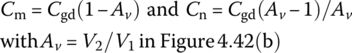
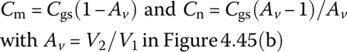
Note also that Ri/Ro are the input/output resistances of the CS amplifier, respectively, and Cm/Cn are the Miller equivalent capacitances for capacitor Cgd seen from the input/output side, respectively (Eq. (1.4.2):
The following MATLAB function ‘break_freqs_of_CS()’ uses Eqs. (4.4.6a,b,c,d) to find the four break frequencies.
4.4.2 CD Amplifier (Source Follower)
Figure 4.45(a) and (b) shows a CD amplifier circuit and its high‐frequency small‐signal equivalent, respectively, where one more load capacitor CLL, in addition to the output capacitor CL, is connected in parallel with the load resistor RL. For the equivalent circuit shown in Figure 4.45(b), a set of three node equations in V1 = Vg, V2 = Vs, and V3 = Vd can be set up as
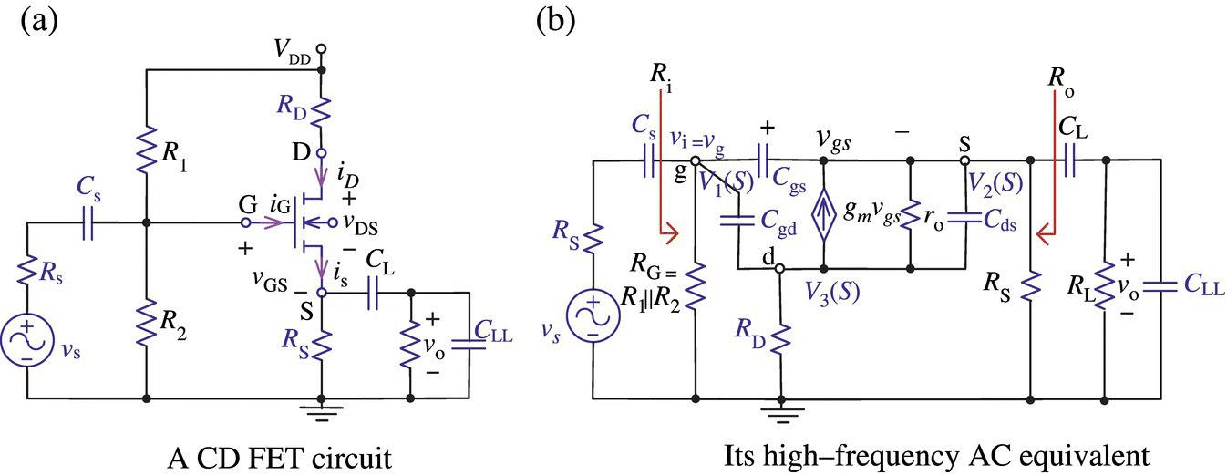
Figure 4.45 A CD (common‐drain) FET circuit and its high‐frequency AC equivalent.
where
- (Q) How about if RD = 0?
- (A) Since V3 = Vd = 0 with RD = 0, Eq. (4.4.8) should be reduced into a 2 × 2 matrix equation in two unknown node voltages V1 and V2.
Solving this set of equations, we can find the transfer function and frequency response:

This process to find the transfer function and frequency response has been cast into the above MATLAB function ‘FET_CD_xfer_ftn()’.
There are four break (pole or corner) frequencies determining roughly the frequency response magnitude:
where Ri/Ro are the input/output resistances of the CD amplifier, respectively, and Cm/Cn are the Miller equivalent capacitances for capacitor Cbe seen from the input/output side, respectively (Eq. (1.4.2)):
Note that Eq. (4.4.11) is just like Eq. (4.4.6) with Cgd and Cgs switched.
The following MATLAB function ‘break_freqs_of_CD()’ uses Eqs. (4.4.11a,b,c,d) to find the four break frequencies:
4.4.3 CG Amplifier
Figure 4.47(a) and (b) shows a CG amplifier circuit and its high‐frequency small‐signal equivalent, respectively, where one more load capacitor CLL, in addition to the output capacitor CL, is connected in parallel with the load resistor RL. Note that if the terminal G(ate) is not AC grounded via a capacitor CG, we should let CG = 0 as shown in Figure 4.47(b). For the equivalent circuit shown in Figure 4.47(b), a set of three node equations in V1 = Vs, V2 = Vd, and V3 = Vg can be set up as
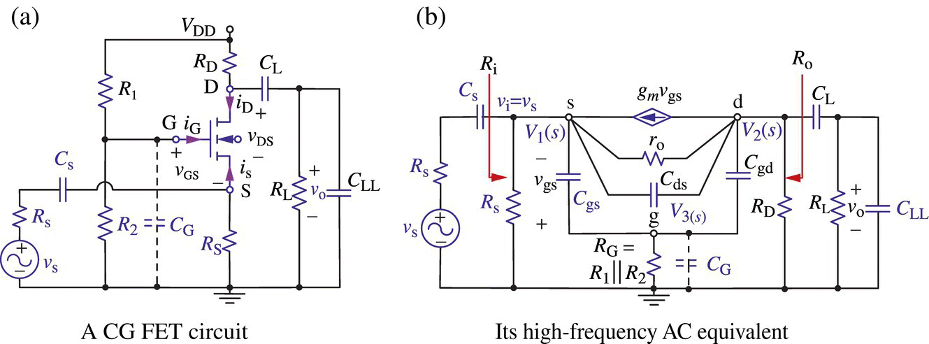
Figure 4.47 A CG (common‐gate) FET circuit and its high‐frequency AC equivalent.
where
- (Q) How about if RG = 0 or CG is so large that RG can be regarded as AC‐shorted?
Solving this set of equations, we can find the transfer function and frequency response:

This process to find the transfer function and frequency response has been cast into the above MATLAB function ‘FET_CG_xfer_ftn()’.
There are five break (pole or corner) frequencies determining roughly the frequency response magnitude:
where Ri/Ro are the input/output resistances of the CG amplifier, respectively.
The following MATLAB function ‘break_freqs_of_CG()’ uses Eqs. (4.4.16a,b,c,d,e) to find the five break frequencies:
4.5 FET Inverter Time Response
In this section, let us see the time response of a basic FET inverter (as shown in Figure 4.16(a) or 4.49(b)) to logic low‐to‐high and high‐to‐low input transitions where low‐to‐high and high‐to‐low propagation delays due to the internal parasitic capacitances between the terminals of the FET can be observed. Note that the effect of the internal parasitic capacitances becomes conspicuous as the frequency or slope of the input increases, while negligible for a DC or low‐frequency input.
Figure 4.49(a) shows a simple DC or large‐signal Spice model of an FET where iD(vGS,vDS) is defined as Eq. (4.1.83) and
- rg: gate resistance, rs: source resistance, rd: drain resistance,
- Cgd: gate‐drain junction capacitance, Cgs: gate‐source junction capacitance,
- Cbd: bulk‐drain junction capacitance, Cbs: bulk‐source junction capacitance.
Figure 4.49(c) shows a DC equivalent of the inverter (Figure 4.49(b)) with the FET replaced by its large‐signal model (Figure 4.49(a)). Like the MATLAB function ‘BJT_inverter_dynamic()’ for the BJT inverter (Figure 3.67(b)), a process of solving the FET inverter to find the output vo(t) to an input vi(t) has been cast into the following MATLAB function ‘FET_inverter_dynamic()’. Note that the drain resistor RD and the (internal) capacitance (Cgd + Cbd) affect how long it takes for Cgd and Cbd to be charged up to VDD, via the time constant during the rising period of vo(t).
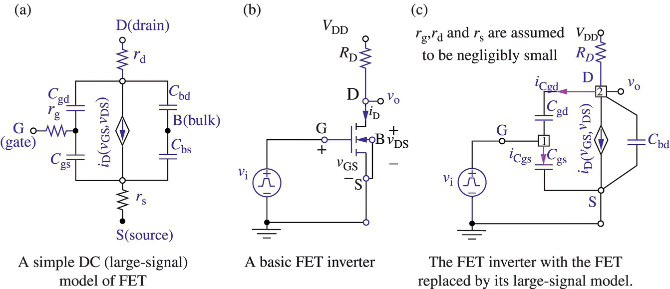
Figure 4.49 A simple large‐signal Spice model of FET and the equivalent of an FET inverter adopting the model.
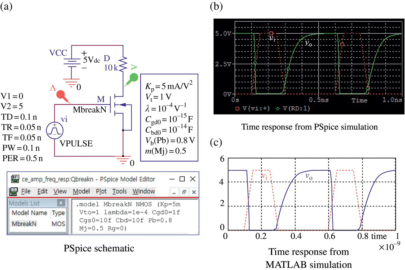
Figure 4.50 A FET inverter and its time response from MATLAB and PSpice (“elec04e19.opj”).
Figure 4.51(a) shows three NMOS inverters, one with no load, one with a purely capacitive load, and one with an RC load. About Figure 4.51(b) showing their input and outputs, note the following:
- The time constant during the rising period of vo1(t) is much longer than that of vo(t) because the equivalent capacitance seen from RD has increased from Cgd + Cbd ≈ 11[fF] to Cgd + (Cbd||CL1) ≈ 1 + 10 + 10 = 21[fF] so that the time constant can be made longer.
- The time constant during the rising period of vo2(t) is about half as long as that of vo1(t) because the equivalent resistance seen from Cbc||CL2 has decreased from RD = 10 kΩ to RD2||RL2 = 10k||10k = 5 [kΩ] so that the time constant can halve.
- (Q4) During the rising period, why does vo2(t) reach just 2.5 V, which is just half of VDD = 5 V unlike vo(t) or vo1(t)?
- (Q5) During the falling period, all the inverter outputs decrease almost linearly as vi(t) increases. Why is that?
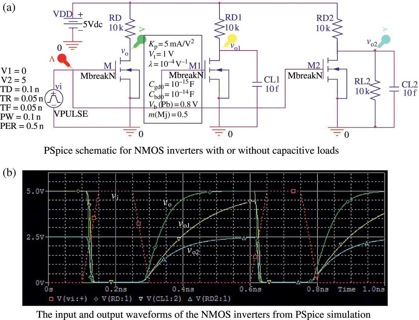
Figure 4.51 NMOS inverters with capacitive loads and their time responses from PSpice (“elec04f51.opj”).
Figure 4.52(a) shows two CMOS (Complementary MOSFET) inverters, one with no load and one with an RC load. About Figure 4.52(b1)/(b2) showing their input and outputs and Figure 4.52(c1)/(c2) showing the currents through Mn and Mp, note the following:
- During the falling period, the output decreases toward 0 almost linearly as vi(t) increases, almost regardless of the load. Why is that? Because, Cgd gets discharged through the NMOS Mn.
- During the rising period, the output increases toward VCC almost linearly as vi(t) decreases, almost regardless of the load. Why is that? Because, Cgd gets charged through the PMOS Mp.
- The current through the CMOS flows only at switching instants when the (internal) capacitors are charged/discharged. Consequently, CMOS logic gates take very little power in a fixed state.
How nice it is of a CMOS inverter to have the (‘rail‐to‐rail’) output swing equal to its input swing with almost no propagation delay and very little static power! That is a primary reason why CMOS has become the most used technology to be implemented in Very Large‐Scale Integration (VLSI) chips.
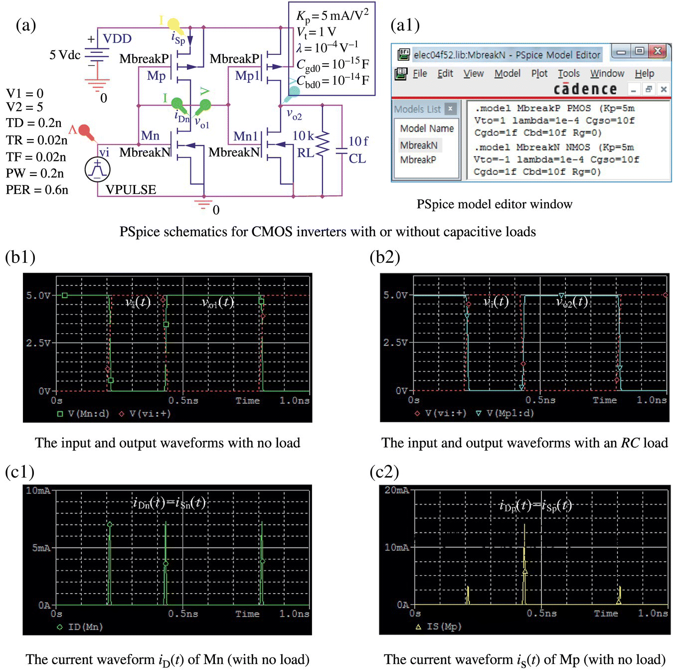
Figure 4.52 CMOS inverter with a capacitive load and its time response from PSpice (“elec04f52.opj”).
Problems
- 4.1 Analysis of JFET Circuits
- Consider the JFET circuit in Figure P4.1(a) where the device parameters of the n‐channel JFET (NJF) J are IDSS = 5 mA/V2, Vt = −5 V, and λ = 0. Find ID, VG, VD, and VS. Also tell which one of the saturation, triode, and cutoff regions the NJF J operates in.
(Hint)>>VDD=12; VG=0; RG=680e3; RD=2e3; RS=1e3;Vt=-5; IDSS=5e-3; Kp=2*IDSS/Vt^2;BETA=Kp/2 % SPICE parameter FET_DC_analysis(VDD,VG,RD,RS,Kp,Vt); - Consider the JFET circuit in Figure P4.1(b) where the device parameters of the NJF J2 are IDSS = 8 mA/V2, Vt = −4 V, and λ = 0. Find ID, VG, VD, and VS. Also tell which one of the saturation, triode, and cutoff regions the NJF J2 operates in.
(Hint)>>VDD=15; R1=1e6; R2=5e5; RD=3e3; RS=1500;Vt=-4; IDSS=8e-3; Kp=2*IDSS/Vt^2; BETA=Kp/2FET_DC_analysis(VDD,R1,R2,RD,RS,Kp,Vt);Noting that it depends on
(P4.1.1)
Figure P4.1 JFET circuits for Problem 4.1.
whether the JFET operates in the saturation or triode region, answer the following questions:
- (b1) Would you decrease or increase R2 to push J2 into the saturation region? With R2 = 200 kΩ and the other parameter values unchanged, tell which region J2 operates in.
- (b2) Would you increase or decrease RD to push J2 into the triode region? With RD = 10 kΩ and the other parameter values as in (b1), tell which region J2 operates in.
- (b3) Would you increase or decrease RS to push J2 into the saturation region? With RS = 10 kΩ and the other parameter values as in (b2), tell which region J2 operates in.
- Noting that the value of BETA, which is one of the SPICE model parameters for a JFET, is determined from IDSS and Vt as
(P4.1.2)
perform the PSpice simulation (with Bias Point analysis type) for the two JFET circuits to check the validity of the circuit analyses done in (a) and (b).
- Consider the JFET circuit in Figure P4.1(a) where the device parameters of the n‐channel JFET (NJF) J are IDSS = 5 mA/V2, Vt = −5 V, and λ = 0. Find ID, VG, VD, and VS. Also tell which one of the saturation, triode, and cutoff regions the NJF J operates in.
- 4.2 Design of a JFET Biasing Circuit
Consider the JFET circuit in Figure P4.2 where the device parameters of the NJF J are IDSS = 12.3 mA/V2, Vt = −3.5 V, and λ = 0. Determine the values of RD and RS so that ID = 1 mA and VDS = 3 V. Check the validity of your design result by using the MATLAB function ‘
FET_DC_analysis()’ and/or PSpice.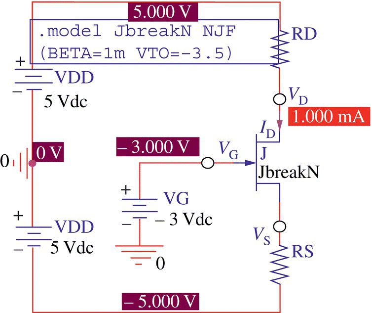
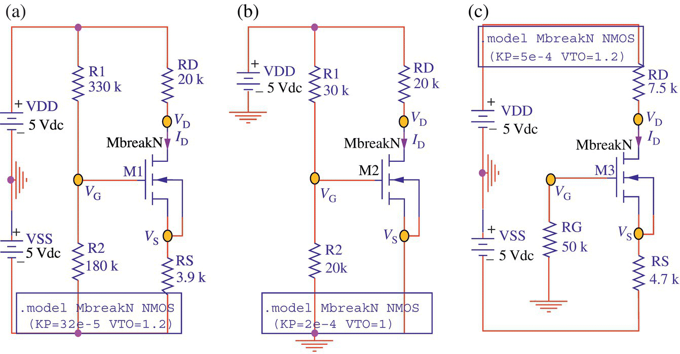
Figure P4.3 NMOS circuits for Problem 4.3.
- 4.3 Analysis of NMOS Circuits
- Consider the NMOS circuit in Figure P4.3(a) where the device parameters of the enhancement NMOS (e‐NMOS) M1 are Kp = 0.32 mA/V2, Vt = 1.2 V, and λ = 0. Find ID, VG, VD, and VS. Also tell which one of the saturation, triode, and cutoff regions the NMOS M1 operates in.
(Hint)>>VDD=5; VSS=-5; R1=330e3; R2=180e3; RD=2e4; RS=3900;Kp=32e-5; Vt=1.2; lambda=0;[VGQ,VSQ,VDQ,VGSQ,VDSQ,IDQ,mode]= ...FET_DC_analysis(VDD-VSS,R1,R2,RD,RS,Kp,Vt,lambda);fprintf('VG=%6.2fV, VD=%6.2fV, VS=%6.2fV, ID=%8.3fmA ',...VGQ+VSS,VDQ+VSS,VSQ+VSS,IDQ*1e3); - Consider the NMOS circuit in Figure P4.3(b) where the device parameters of M2 are Kp = 0.2 mA/V2, Vt = 1 V, and λ = 0. Find ID, VG, VD, and VS. Also tell which region M2 operates in.
- Consider the NMOS circuit in Figure P4.3(c) where the device parameters of the e‐NMOS M3 are Kp = 0.5 mA/V2, Vt = 1.2 V, and λ = 0. Find ID, VG, VD, and VS. Also tell which region the NMOS M3 operates in. Plot the load line for iD = (VG − VSS − vGS)/RS on the iD‐vGS characteristic curve for iD = Kp(vGS − Vt)2/2 and locate the operating point (VGS,Q, ID,Q). Also plot the load line for iD = (VDD − VSS − vDS)/(RD + RS) on the iD‐vDS characteristic curve (with vGS = VGS,Q) and locate the operating point. To those ends, complete and run the following script:
- Perform the PSpice simulation (with Bias Point analysis type) for the three NMOS circuits to check the validity of the circuit analyses done in (a), (b), and (c).
- Consider the NMOS circuit in Figure P4.3(a) where the device parameters of the enhancement NMOS (e‐NMOS) M1 are Kp = 0.32 mA/V2, Vt = 1.2 V, and λ = 0. Find ID, VG, VD, and VS. Also tell which one of the saturation, triode, and cutoff regions the NMOS M1 operates in.
- 4.4 Analysis PMOS Circuits
- Consider the PMOS circuit in Figure P4.4(a1) where the device parameters of the enhancement PMOS (e‐PMOS) M1 are Kp = 0.2 mA/V2, Vt = −0.4 V, and λ = 0. Find ID, VG, VD, and VS. Also tell which one of the saturation, triode, and cutoff regions the NMOS M1 operates in.
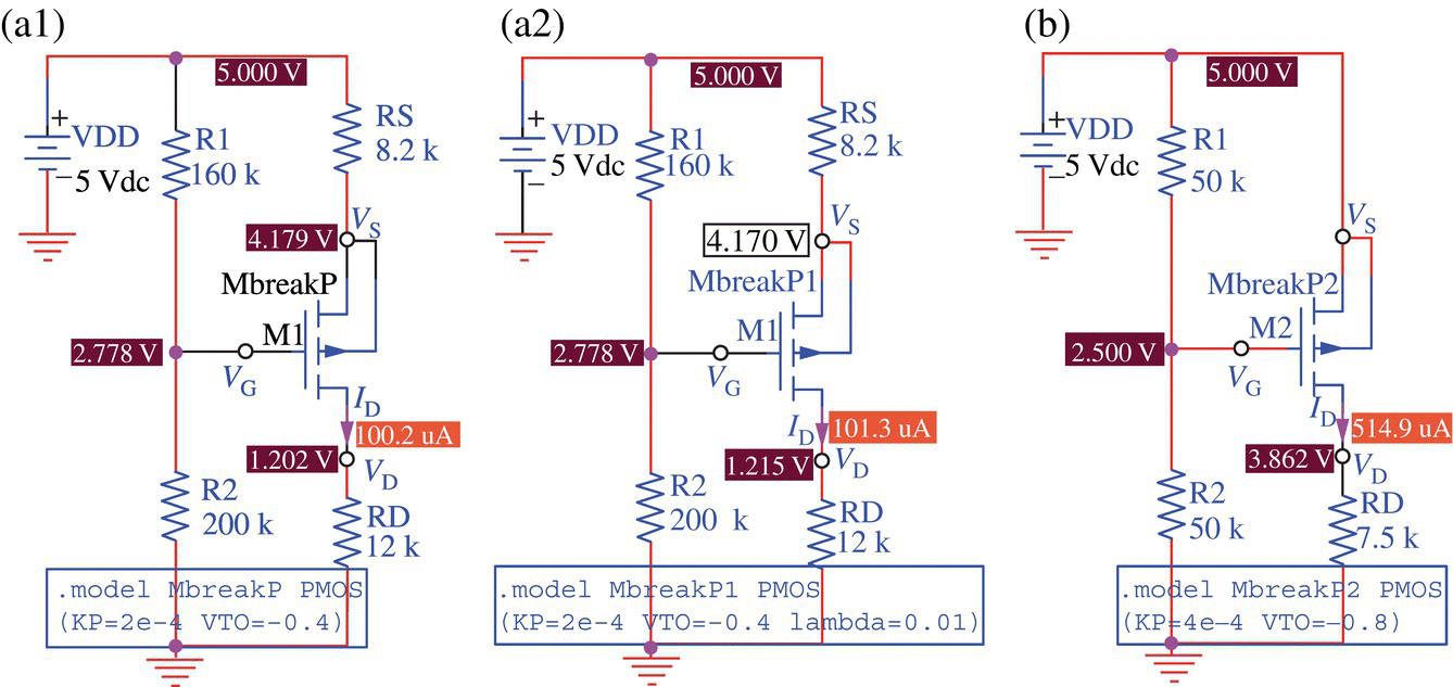
Figure P4.4 PMOS circuits.
(Hint)>>VDD=5; R1=160e3; R2=200e3; RS=8.2e3; RD=12e3;Kp=2e-4; Vt=-0.4; lambda=0; % Device parametersFET_PMOS_DC_analysis(VDD,R1,R2,RS,RD,Kp,Vt,lambda); - Consider the PMOS circuit in Figure P4.4(a2) where the device parameters of the e‐PMOS M1 are Kp = 0.2 mA/V2, Vt = −0.4 V, and λ = 0.01. Find ID, VG, VD, and VS. Also tell which region the PMOS M1 operates in.
- Consider the PMOS circuit in Figure P4.4(b) where the device parameters of the e‐PMOS M2 are Kp = 0.4 mA/V2, Vt = −0.8 V, and λ = 0.01. Find ID, VG, VD, and VS. Also tell which region the PMOS M2 operates in.
- Perform the PSpice simulation (with Bias Point analysis type) for the three PMOS circuits to check the validity of the circuit analyses done in (a), (b), and (c).
- Consider the PMOS circuit in Figure P4.4(a1) where the device parameters of the enhancement PMOS (e‐PMOS) M1 are Kp = 0.2 mA/V2, Vt = −0.4 V, and λ = 0. Find ID, VG, VD, and VS. Also tell which one of the saturation, triode, and cutoff regions the NMOS M1 operates in.
- 4.5 Design of a MOSFET biasing Circuit
Consider the MOSFET circuit in Figure P4.5 where the device parameters of the NMOS M1 are Kp = 1 mA/V2, Vt = 1.2 V, and λ = 0. Determine the values of RD, RS, R1, and R2 so that ID = 0.4 mA, VD = 6 V, VDS = 3.1 V, and Ri = 100 kΩ. Check the validity of your design result by using the MATLAB function ‘
FET_DC_analysis()’ and/or PSpice.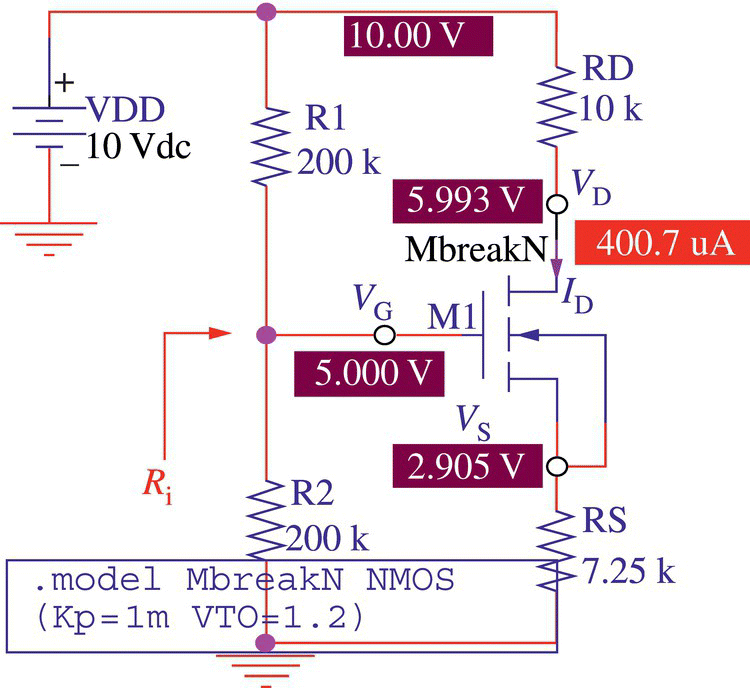
- 4.6 Diode‐Connected MOSFETs Used as Nonlinear Resistors
Consider the two NMOS circuits in Figure P4.6 where the device parameters of the enhancement NMOS (e‐NMOS) M1 and the depletion NMOS (d‐NMOS) M2 are Kp1 = 0.02 mA/V2, Vt1 = 1 V, λ1 = 0 and Kp2 = 0.02 mA/V2, Vt2 = −3 V, λ2 = 0, respectively.
- Perform the load line analysis of finding the operating points Q1/Q2 from the intersections between the iDk‐vDSk characteristice curves of M1/M2 and the load line for iDk = (VDD − vDSk)/Rk where the load lines for M1/M2 are identical since R1 = R2. If helpful, complete and run the corresponding part of the following MATLAB script “elec04p06.m” to plot the related graphs and find the operating points for M1/M2.

Figure P4.6 Diode‐connected MOSFET circuits.
- As a nonlinear approach, use the MATLAB function ‘
fsolve()’ to solve the following KCL equations:(P4.6.1) (P4.6.2)
where iDk(vGSk,vDSk) is defined as Eq. (4.1.83) and implemented by the MATLAB function ‘
iD_NMOS_at_vDS_vGS()’ (see the end of Section 4.1.1), which is stored in a separate m‐file named “iD_NMOS_at_vDS_vGS.m.” If helpful, complete and run the corresponding part of the above MATLAB script “elec04p06.m” to find the operating points for M1/M2. - Perform the PSpice simulation (with Bias Point analysis type) for the two MOSFET circuits to check the validity of the operating points found in (a) or (b). Also, perform the PSpice simulation (with DC Sweep analysis type) for the two MOSFETs (with R1/R2 short‐circuited for removal) to get the iDk‐vDSk characteristice curves of M1/M2 (for VDD = 0 : 0.01 : 8 V) and see if they conform with those obtained in (a) or plotted in Figure 4.13(c1).
- Perform the load line analysis of finding the operating points Q1/Q2 from the intersections between the iDk‐vDSk characteristice curves of M1/M2 and the load line for iDk = (VDD − vDSk)/Rk where the load lines for M1/M2 are identical since R1 = R2. If helpful, complete and run the corresponding part of the following MATLAB script “elec04p06.m” to plot the related graphs and find the operating points for M1/M2.
- 4.7 Cascode Current Mirror
Consider the cascode current mirror circuit in Figure P4.7 where the four NMOSs have the device parameters Kp = 1 mA/V2, Vt = 1 V, and λ = 2 mV−1 in common.
- Noting that vGS1 = vDS1 = v1 and vGS3 = vDS3 = v3 − v1, apply KCL at nodes 1, 2, and 3 to write the node equations:
(P4.7.1a)
 (P4.7.1b)
where iDk(vGSk,vDSk) is defined as Eq. (4.1.83) and implemented by the MATLAB function ‘
iD_NMOS_at_vDS_vGS()’ (see the end of Section 4.1.1). If a current source I is connected into node 3, how will Eq. (P4.7.1c) be changed? - Noting that the small‐signal resistance of an e‐NMOS with G‐D connected is 1/gm (Eq. (4.1.19), we can draw the small‐signal equivalent of the circuit as Figure P4.7(c). To find the output resistance Ro, we apply a test current source iT into node D4 and write the KCL equations at nodes D4 and 2:
(P4.7.3)
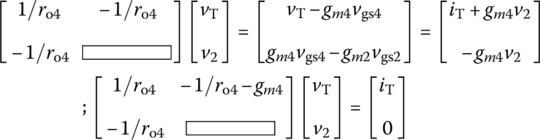
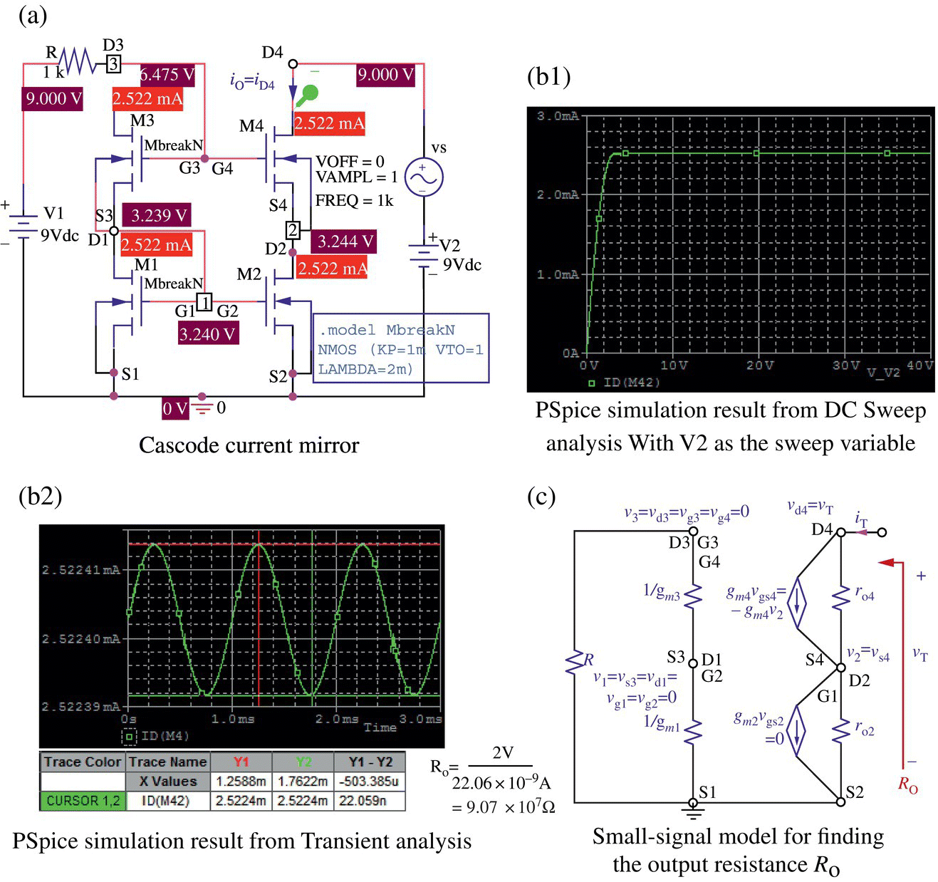
Figure P4.7 Cascode current mirror using FETs (“elec04p07.opj”).
We can solve this equation and find the output resistance:
where no current flows in the left part with no source so that v3 = vd3 = vg3 = vg4 = 0 and v1 = vs3 = vd1 = vg1 = vg2 = 0.
(Q) In the small‐signal equivalent shown in Figure P4.7(c), why have M1 and M3 been modeled by just a resistor of 1/gm (with no current source) unlike M2 and M4?
- Complete the above MATLAB function ‘
FET4_current_mirror_cascode()’, which implements Eqs. (P4.7.1/2) and (P4.7.4) for analyzing a cascode current mirror (excited by a voltage source V1 or a reference current source I) and finding its output resistance. Use the MATLAB function to find the output current io versus V2 = 0:0.01:40 and plot it. Also, find the output resistance Ro (when V2 = 9 V) of the current mirror (shown in Figure P4.7(a)) two times, once when it is excited by a voltage source V1 of 9 V (with a resistance R of 1 kΩ) and once when it is excited by a current source of I = 2.5 mA. - Perform the PSpice simulation of the circuit excited by a voltage source V1 of 9 V (with a resistance R of 1 kΩ) two times, once with DC Sweep analysis to get the plot of the output current io versus V2 = 0:0.01:40 (sweep variable) as depicted in Figure P4.7(b1) and once with Transient analysis to get the plot of io versus t = 0 : 1 μs : 3 ms to the AC voltage source vs (of amplitude 1 V and frequency 1 kHz) as depicted in Figure P4.7(b2). Is the first graph (Figure P4.7(b1)) similar to the plot of io versus V2 obtained in (c)? From the second graph (Figure P4.7(b2)), find the (small‐signal) output resistance:
(P4.7.5)
Is it close to that obtained in (c)?
- Noting that vGS1 = vDS1 = v1 and vGS3 = vDS3 = v3 − v1, apply KCL at nodes 1, 2, and 3 to write the node equations:
- 4.8 CMOS Inverter
Consider the CMOS inverter in Figure 4.19(a) where VDD = 10 V and the NMOS/PMOS have the device parameters KpN = 200 μA/V2, VtN = 2 V, KpP = 80 μA/V2, VtP = −2 V, and λ = 0.
- To determine the point (VIL,VOH) with the slope of −1 in Region II (where Mn and Mp are in the saturation and ohmic regions, respectively), we write the KCL equation at the output node (Dp,Dn):
(P4.8.1a)

Differentiating both sides w.r.t. vi and substituting dvo/dvi = −1 yields

Use the MATLAB function ‘
fsolve()’ to solve this set of two equations and find (VIL,VOH) by running the following statements:>>VDD=10; KN=2e-4; KP=8e-5; VtN=2; VtP=-2; Kr2=KN/KP; Kr=sqrt(Kr2)Vm=(VDD+VtP+Kr*VtN)/(1+Kr); % Eq. (4.1.65)eq_VIL=...@(v)[(VDD-v(1)+VtP)*(VDD-v(2))-(VDD-v(2))^2/2-Kr2*(v(1)-VtN)^2/2;v(2)-(VDD+v(1)-VtP+Kr2*(v(1)-VtN))/2]; % Eq. (P4.8.1a,b)v=fsolve(eq_VIL,[Vm Vm]); VIL=v(1), VOH=v(2)Check if these values conform with those obtained by using Eq. (16.61) or (16.63) of [N-1] depending on KpN/KpP = 1 or not:
and substituting vi = VIL into Eq. (P4.8.1b):
>>VIL_Neamen=(VtN+(VDD+VtP-VtN)/(Kr2-1)*(2*sqrt(Kr2/(Kr2+3))-1))...*(Kr~=1) + (Kr==1)*(VtN+3/8*(VDD+VtP-VtN)); %Eq. (P4.8.2)VOH_Neamen=((1+Kr2)*VIL_Neamen+VDD-Kr2*VtN-VtP)/2; % Eq. (P4.8.1b)[VIL VIL_Neamen VOH VOH_Neamen] % Do they conform each other? - To determine the point (VIH,VOL) with the slope of −1 in Region IV (where Mn and Mp are in the ohmic and saturation regions, respectively), we write the KCL equation at the output node (Dp,Dn):
(P4.8.3a)
Differentiating both sides w.r.t. vi and substituting dvo/dvi = −1 yields
We can use the MATLAB function ‘
fsolve()’ to solve this set of two equations and find (VIH,VOL) by running the following statements:>>eq_VIH=@(v)[Kr2*((v(1)-VtN)*v(2)-v(2)^2/2)-(VDD-v(1)+VtP)^2/2;v(2)+((VDD-v(1)+VtP)/Kr2-v(1)+VtN)/2]; % Eq. (P4.8.3a,b)v=fsolve(eq_VIH,[Vm Vm]); VIH=v(1), VOL=v(2)Check if these values conform with those obtained by using Eq. (16.66) or (16.69) of [N-1] depending on KpN/KpP = 1 or not:
and substituting vi = VIH into Eq. (P4.8.3b):
>>VIH_Neamen=(VtN+(VDD+VtP-VtN)/(Kr2-1)*(2*Kr2/sqrt(3*Kr2+1)-1))...*(Kr~=1) + (Kr==1)*(VtN+5/8*(VDD+VtP-VtN)); %Eq. (P4.8.4)VOL_Neamen=(VIH_Neamen*(1+1/Kr2)-VtN-(VDD+VtP)/Kr2)/2; %(P4.8.3b)[VIH VIH_Neamen VOL VOL_Neamen] % Do they conform each other? - Complete and run the above MATLAB script “elec04p08.m” to plot the VTC together with the critical points as depicted in Figure P4.8(a) and the iD‐vDS characteristic curves (for Mn and Mp) as depicted in Figure P4.8(b).
Figure P4.8 VTC curve of a CMOS inverter and the iD‐vDS characteristic curves of NMOS/PMOS.
- Find the points on the iD‐vDS characteristic curves (shown in Figure P4.8(b)) corresponding to each of the points A, T1, M, T2, and B on the VTC (shown in Figure P4.8(a)). Explain the meaning of each point.
- To determine the point (VIL,VOH) with the slope of −1 in Region II (where Mn and Mp are in the saturation and ohmic regions, respectively), we write the KCL equation at the output node (Dp,Dn):
- 4.9 CMOS Differential (or Source‐Coupled) Pair Loaded by a Current Mirror
Consider the CMOS differential pair loaded by a current mirror in Figure P4.9.1(a) where VDD = 6 V, VGG = 4 V, VSS = 2 V, and the NMOS/PMOS have the device parameters KpN = 2 mA/V2, VtN = 1 V, KpP = 2 mA/V2, VtP = −1 V, and λ = 0.02 V−1.
- Noting that vGS1 = VGG + vd − v3, vDS1 = v1 − v3, vGS2 = VGG − v3, vDS2 = v2 − v3, and vSG3 = vSD3 = VDD − v1, vSG4 = VDD − v1, and vSD4 = VDD − v2, apply KCL at nodes 1, 2, and 3 to write the node equations:
(P4.9.1a)
 (P4.9.1b)
 (P4.9.1c)
where iD1(vGS1,vDS1) = iD2(vGS2,vDS2) = iDn(vGS,vDS) and iD3(vSG3,vSD3) = iD4(vSG4,vSD4) = iDp(vSG,vSD), defined as Eq. (4.1.83), can be implemented by the MATLAB function handles ‘
iDn()’ and ‘iDp()’, respectively, in the MATLAB function ‘FET_differential_loaded_ by_current_mirror()’ below. - Noting from Eqs. (3.78) and (3.79) of [C-1] that the output resistance (seen from node 2 and ground) and voltage gain of the differential pair are
complete the above MATLAB function ‘
FET_differential_loaded_by_current_mirror()’, which solves Eq. (P4.9.1) for v1, v2, and v3, and also uses Eqs. (P4.9.2,3) to find the output resistance and voltage gain. - Run the above MATLAB script “elec04p09.m,” which uses the MATLAB function ‘
FET_ differential_loaded_by_current_mirror()’ two times, once with the fifth input argument vds = [−1.5 : 0.015 : 1.5] to plot iD1/iD2 versus vd on a graph (as depicted in Figure P4.9.1(b1)) and v1/v2/v3 versus vd on another graph (as depicted in Figure P4.9.1(b2)), and once the fifth input argument vds = [vd(t); t] (t = 0 : 1 μs : 3 ms) to plot vd(t)/Avvd(t)/vo(t) = v2(t)‐mean(v2(t)) versus t on another graph (as depicted in Figure P4.9.2(a1)) where vd(t) = sin (2000πt) [mV]. You will see not only the related graphs but also the theoretical values of the output resistance and voltage gain.
Figure P4.9.1 CMOS differential (source‐coupled) pair loaded by a current mirror (“FET_differential_loaded_by_current mirror.opj”).
- Constructing the schematic as depicted in Figure P4.9.1(a), perform the PSpice simulation of DC Sweep analysis with the sweep variable vd = −1.5 : 0.01 : 1.5 [V] to get the plot of iD1/iD1 versus vd on a graph (as depicted in Figure P4.9.1(c1)) and v1/v2/v3 versus vd on another graph (as depicted in Figure P4.9.1(c2)). Are they similar to the MATLAB analysis results shown in Figure P4.9.1(b1) and (b2)? Also perform the PSpice simulation of Transient analysis on the output voltage v2 to the sinusoidal input differential voltage source vdSIN = sin (2000πt) [mV] to measure the voltage gain Av = v2/vdSIN. Is it close to the MATLAB analysis result obtained in (c)?
- Constructing the schematic (applying a test current source iT = sin (2000πt)[μA] into the output node 2) as depicted in Figure P4.9.2(b), perform the PSpice simulation of Transient analysis on the voltage vT across the test current source to measure the output resistance Ro = vT/iT. Is it close to the MATLAB analysis result obtained in (c)?
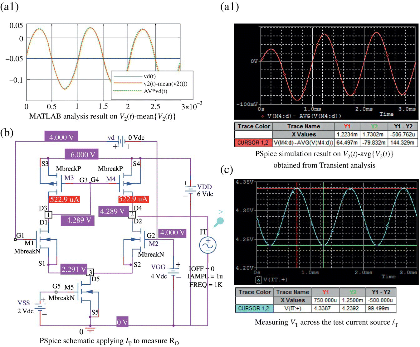
Figure P4.9.2 CMOS differential (or source‐coupled) pair loaded by a current mirror.
- Noting that vGS1 = VGG + vd − v3, vDS1 = v1 − v3, vGS2 = VGG − v3, vDS2 = v2 − v3, and vSG3 = vSD3 = VDD − v1, vSG4 = VDD − v1, and vSD4 = VDD − v2, apply KCL at nodes 1, 2, and 3 to write the node equations:
- 4.10 Analysis of CS JFET Amplifier Circuit
Consider the JFET circuit in Figure P4.10(a) where the JFET has the device parameters BETA = Kp/2 = 0.75 mA/V2, VTO = Vt = −4 V, and λ = 0.008 V−1.
- Complete the following MATLAB script “elec04p10.m” so that it can use the MATLAB function ‘
FET_CS_analysis()’ to analyze the circuit three times, once with RD = 2.7 kΩ and RS = 2.7 kΩ (case A), once with RD = 2.7 kΩ and RS = 5 kΩ (case B), and once with RD = 3.5 kΩ and RS = 5 kΩ (case C). Then, run it to find the overall voltage gain Gv = vo/vi for the three cases. Noting that the three output voltage waveforms in Figure P4.10(c) have been obtained from PSpice simulations for the three cases with the small‐signal input vi(t) = 0.1 sin (2000πt), identify which one of voa(t), vob(t), and voc(t) corresponds to the output voltage of three cases A, B, and C, respectively.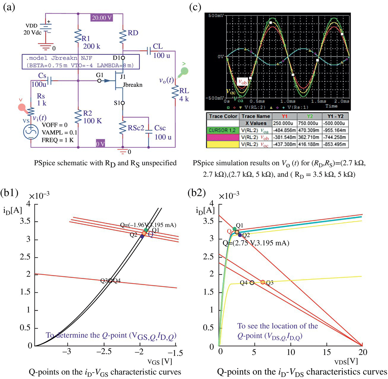
Figure P4.10 A CS JFET amplifier and its analysis based on the operating points.
- Figure P4.10(b1) and (b2) shows the three Q‐points Q, Q3, and Q4 on the iD‐vGS and iD‐vDS characteristic curves for the three cases A, B, and C. Based on the slopes of the load lines crossing the Q‐points, rather than the DC analysis results obtained in (a), identify which one of Q, Q3, and Q4 corresponds to each of the three cases, respectively, and write the equations for the related load lines. From the locations of the three Q‐points, tell which case is the most susceptible to the output distortion for an increasing amplitude of the input voltage vi(t).
- To see how easily the output vo(t) gets distorted by raising the amplitude of the small‐signal input increasing vi(t), two more Q‐points Q1 and Q2 with VG = 20/3±0.2[V] have been drawn in Figure P4.10(b1) and (b2). Which one of them corresponds to each of VG = 20/3±0.2[V], respectively?
- Considering the above three cases for which the small‐signal output voltage waveforms are shown in Figure P4.10(b), can you say that the maximum small‐signal output voltage that can be produced with no distortion is proportional to the voltage gain Gv?
- Are you going to increase or decrease the value of RS1 to push the Q‐point rightward towards VDD? Will the possibility of output distortion be decreased by moving the Q‐point rightward, i.e. increasing VDS,Q? Generally speaking, if a Q‐point is too close to vDS = VDD, can the output easily get distorted from the lower or upper part?
- The output voltage waveforms shown in Figure P4.10(c) have larger/smaller magnitdes when they are negative/positive. To figure out what makes such a difference, find out the relationship among the slope of the iD‐vGS characteristic curve (Figure P4.10(b1)), the transconductance gm, and the voltage gain Gv = vo/vi. Based on the relationship and considering the difference between the slopes of the iD‐vGS characteristic curve on the left/right part of a Q‐point, explain the difference between the magnitudes of vo(t) during its positive/negative periods.
- Complete the following MATLAB script “elec04p10.m” so that it can use the MATLAB function ‘
- 4.11 Analysis of CS MOSFET Amplifier Circuit
Consider the MOSFET circuit in Figure P4.11(a) where the NMOS has the device parameters Kp = 2 mA/V2, Vt = 0.8 V, and λ = 0 V−1.

Figure P4.11 A CS MOSFET amplifier, its load line analysis, and PSpice simulation result.
- Complete the above MATLAB script “elec04p11.m” so that it can use the MATLAB function ‘
FET_CS_analysis()’ to analyze the circuit three times, once with Kp = 1.6 mA/V2 and without a bypass capacitor CSc in parallel with RSc (case A), once with Kp = 2 mA/V2 and without CSc (case B), and once with Kp = 2 mA/V2 and CSc in parallel with RSc (case C). Then, run it to find the voltage gain Gv = vo/vi for the three cases. - Which case is the DC analysis result (obtained from the PSpice simulation) displayed on the schematic in Figure P4.11(a) for?
- Figure P4.11(b1) and (b2) shows the DC/AC load lines and Q‐points on the iD‐vGS characteristic curves for the cases B (without CSc) and C (with CSc). Write the equation for the DC load line and find the slopes of the AC load lines for the two cases. From the load lines and corresponding Q‐points swaying with the small‐signal input voltage vi = ΔvG, tell which case will produce a larger small‐signal drain current id for the same amplitude of vi, yielding a larger small‐signal output voltage like vob(t) in Figure P4.11(c).
- Find the small‐signal voltage gains for voa(t) and vob(t) in the PSpice simulation result (Figure P4.11(c)) and check if they are close to the MATLAB analysis result obtained in (a).
- Complete the above MATLAB script “elec04p11.m” so that it can use the MATLAB function ‘
- 4.12 Analysis of CD MOSFET Amplifier (Source Follower) Circuit
Consider the MOSFET circuit in Figure P4.12(a) where the NMOS has the device parameters Kp = 1 mA/V2, Vt = 1 V, and λ = 0.025 V−1.
- Complete the following MATLAB script “elec04p12.m” so that it can use the MATLAB function ‘
FET_CD_analysis()’ to analyze the circuit three times, once with RD = 20 kΩ and RS = 20 kΩ (case A), once with RD = 35 kΩ and RS = 20 kΩ (case B), and once with RD = 20 kΩ and RS = 35 kΩ (case C). Then, run it to find the voltage gain Gv = vo/vi and the input/output resistances for the three cases. Do the changes of the voltage gain and the input/output resistances due to the change of RD or RS conform with your expectation based on Eqs. (4.2.11a), (4.2.12), and (4.2.10)?
Figure P4.12 A CD MOSFET amplifier and its PSpice simulation result.
- Check if the PSpice simulation results on the voltage gain Gv = vo/vi (shown in Figure P4.12(b)) agree with the MATLAB analysis results.
- Complete the following MATLAB script “elec04p12.m” so that it can use the MATLAB function ‘
- 4.13 Analysis of CG MOSFET Amplifier
Consider the MOSFET circuit in Figure P4.13(a1) or (a2) where the NMOS has the device parameters Kp = 1 mA/V2, Vt = 1 V, and λ = 0.01 V−1. Complete and run the following MATLAB script “elec04p13.m” to find the voltage gain Gv = vo/vi and the input/output resistances. Then see if they conform with the PSpice simulation results shown in Figure P4.13(b1) and (b2).
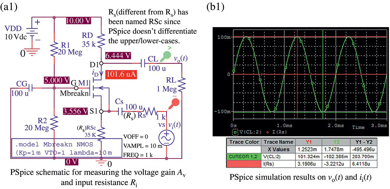

Figure P4.13 A CG MOSFET amplifier and its PSpice simulation result.
- 4.14 Analysis of Multistage MOSFET Amplifier
Consider the two‐stage MOSFET circuit in Figure P4.14(a) where the device parameters of the NMOSs M1 and M2 are Kp1 = 1 mA/V2, Vt1 = 1.2 V, λ1 = 0 V−1, Kp2 = 0.4 mA/V2, Vt2 = 1.2 V, and λ2 = 0 V−1. Noting that the input resistance Ri2 of stage 2 is infinite so that stage 1 (consisting of M1, R11, R21, RD1, and RSc) can be analyzed first, independently of stage 2 (consisting of M2 and RSc2), complete and run the following MATLAB script “elec04p14.m” to find the overall voltage gain Gv = vo/vi and the overall input/output resistances. Then see if they conform with the PSpice simulation results shown in Figure P4.14(b).
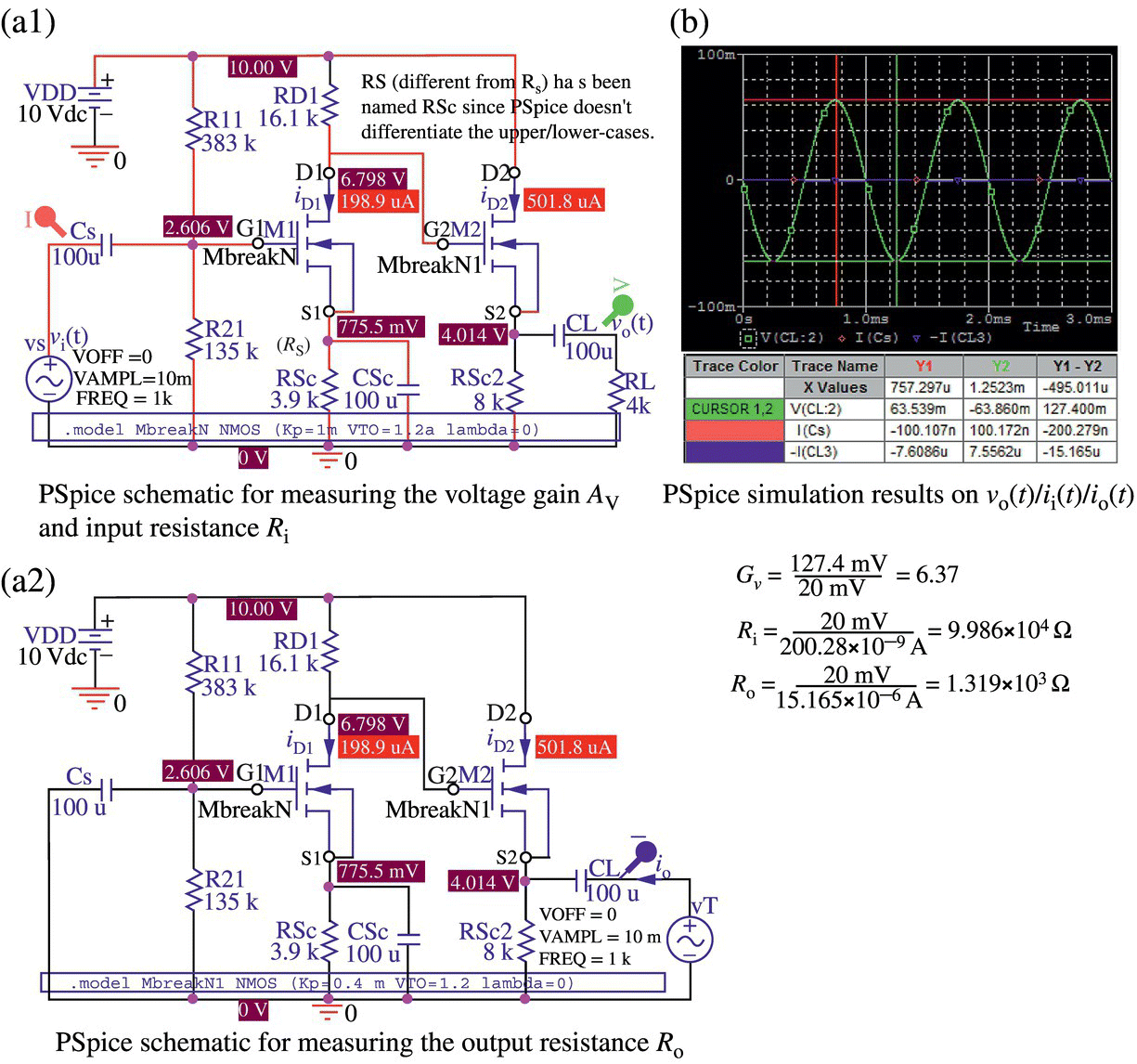
Figure P4.14 A two‐stage amplifier and its PSpice simulation result.
- 4.15 Analysis of a Two‐Stage MOSFET Amplifier
Consider the MOSFET circuit in Figure P4.15(a) where the device parameters of the NMOSs M1 and M2 are Kp1 = 2 mA/V2, Vt1 = 0.8 V, λ1 = 0 V−1, Kp2 = 1 mA/V2, Vt2 = 1 V, and λ2 = 0 V−1. Noting that in general the analysis of a multistage amplifier needs performing a provisional backward analysis (starting from the last stage with the overall load resistance RL) to determine the input resistances of each stage and then performing a forward analysis (starting from the first stage with the overall source resistance Rs) to determine the voltage gain and output resistances of each stage, complete the above MATLAB script “elec04p15.m” so that it can use the MATLAB function ‘
FET_CD_ analysis()’ to analyze stage 2, ‘FET_CS_analysis()’ to analyze stage 1, and ‘FET_CD_ analysis()’ to analyze stage 2 again. Run it to find the overall voltage gain Gv = vo/vi and the overall input/output resistances RI/RO. Compare the overall voltage gain Gv with that obtained from the PSpice simulation (shown in Figure P4.15(b)) to see how close they are. Explain how the voltage gain has become larger than that of the single‐stage amplifier without the stage 2 (of CD configuration) whose voltage gain is less than 1 (Problem 4.12).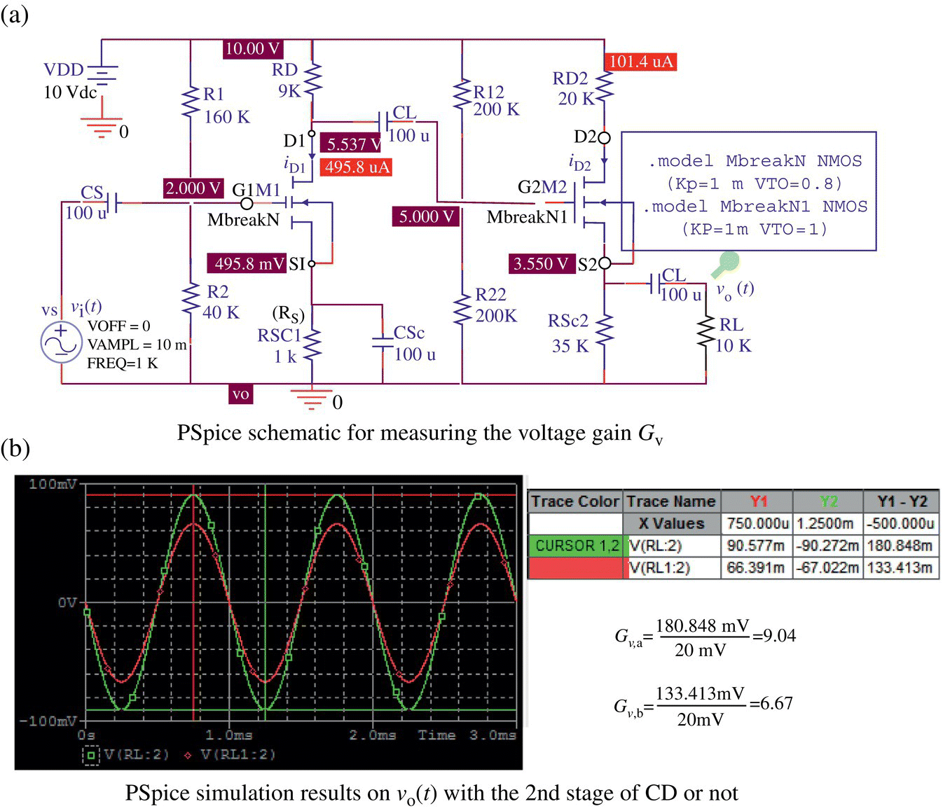
Figure P4.15 A two‐stage amplifier and its PSpice simulation result.
- 4.16 Analysis of a Three‐Stage MOSFET Amplifier
Consider the MOSFET circuit in Figure P4.16(a) where the device parameters of the NMOSs M1/M3 are Kp = 1 mA/V2, Vt = 1 V, λ = 0.01 V−1 in common, and those of the NPN‐BJT Q2 are βF = 100, βR = 1, VA = 100 V, and Is = 10−16 V. Noting that in general the analysis of a multistage amplifier needs performing a provisional backward analysis (starting from the last stage with the overall load resistance RL) to determine the input resistances of each stage and then performing a forward analysis (starting from the first stage with the overall source resistance Rs) to determine the voltage gain and output resistances of each stage, complete the following MATLAB script “elec04p16.m” so that it can use the MATLAB function ‘
FET_CD_analysis()’ to analyze stage 3 (of CD configuration), ‘BJT_CE_analysis()’ to analyze stage 2 (of CE configuration), and ‘FET_CS_analysis()’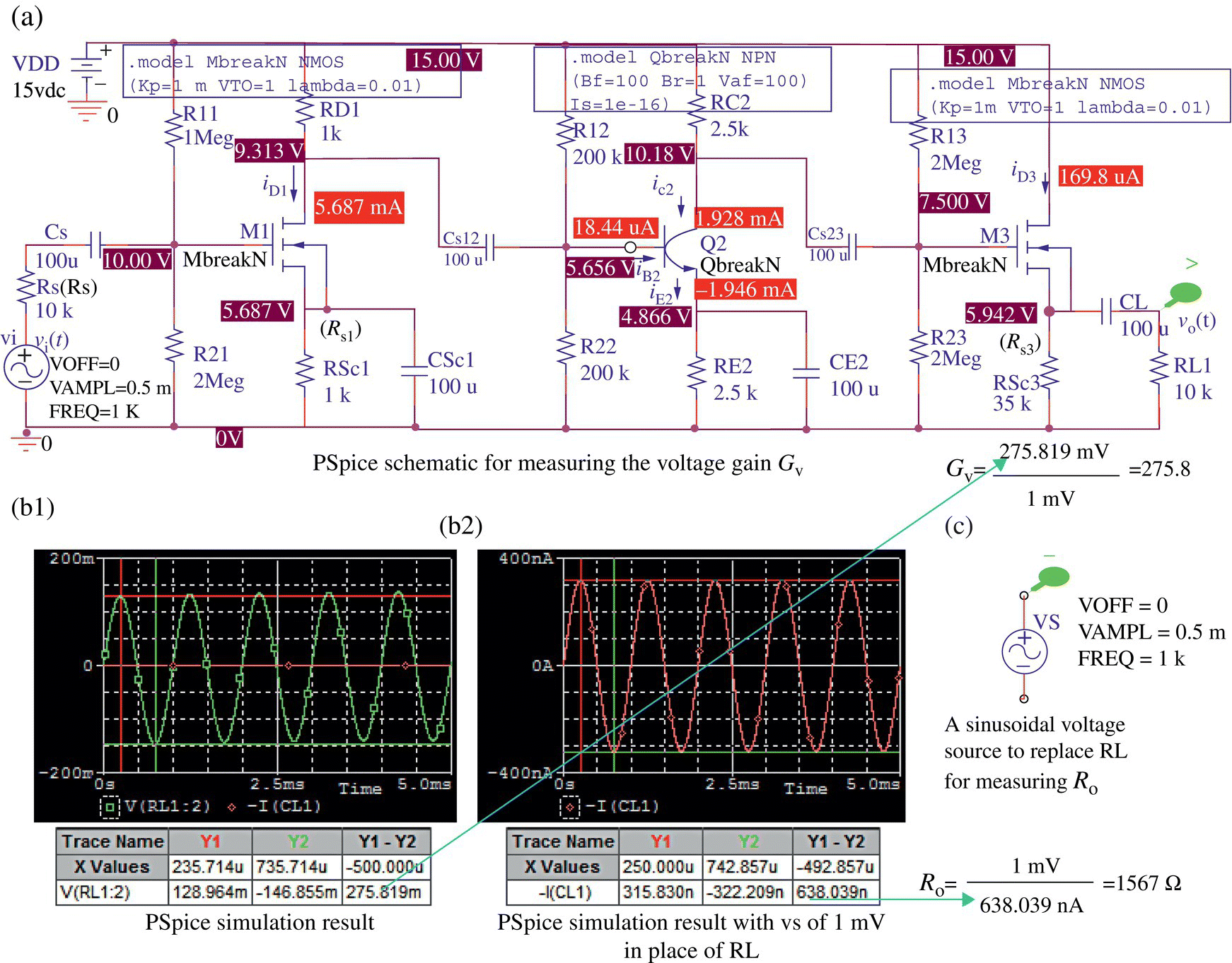
Figure P4.16 A three‐stage amplifier and its PSpice simulation result.
to analyze stage 1 (of CS configuration), ‘
BJT_CE_analysis()’ to analyze stage 2, and ‘FET_CD_analysis()’ to analyze stage 3. Run it to find the overall voltage gain Gv = vo/vi and the overall input/output resistances RI/RO. Compare the overall voltage gain Gv with that obtained from the PSpice simulation (shown in Figure P4.16(b1)) to see how close they are. - 4.17 Cascode MOSFET Amplifiers
Consider the FET cascode amplifier circuits in Figure P4.17 where the NMOSs have the device parameters Kp = 1 mA/V2, Vt = 1 V, and λ = 10−4 V−1 in common.
- For the FET cascode amplifier A (in Figure P4.17(a)) with R1 + R2 + R3 = 500 kΩ and RS(RSc) = 8 kΩ, determine the values of the resistors R1, R2, R3, and RD so that ID,Q = 0.5 mA and VDS1,Q = VDS2,Q = 2.5 V in the saturation mode.
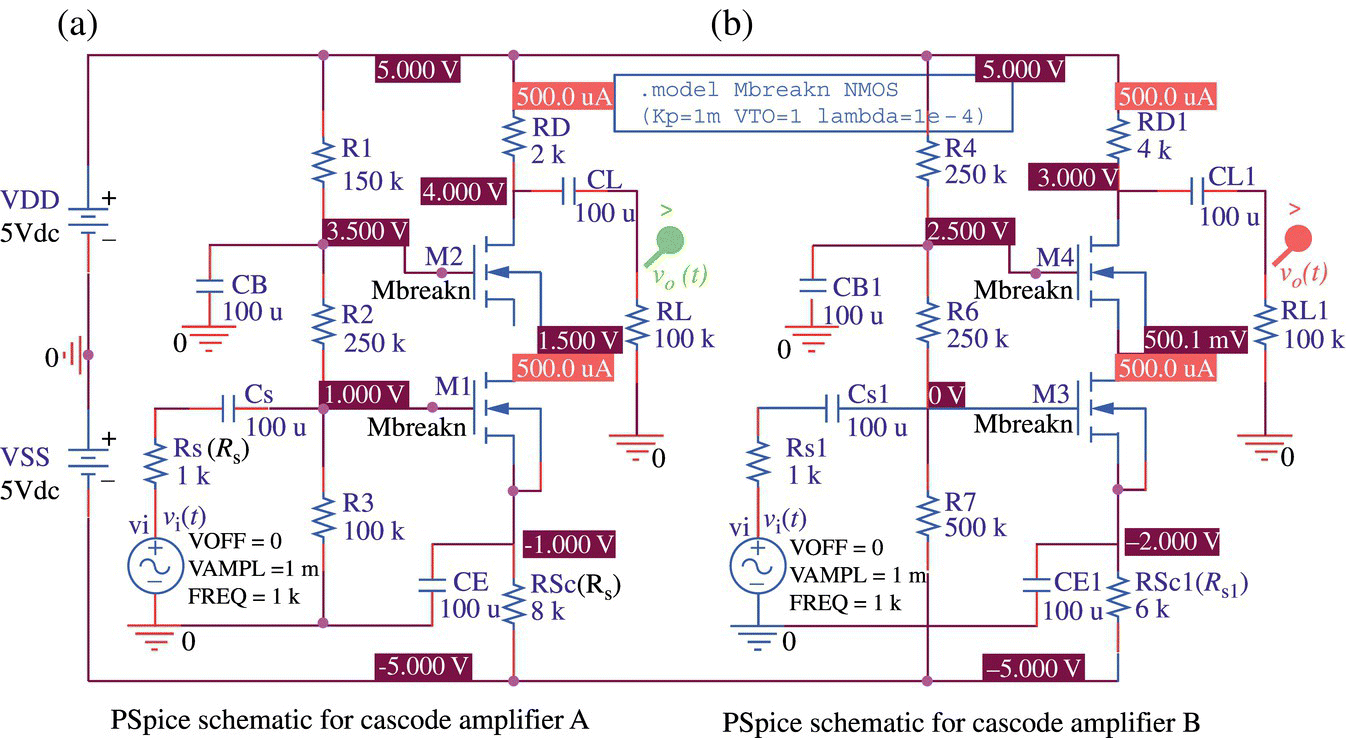
Figure P4.17 PSpice schematics for two cascode amplifier circuits.
- Complete the former part of the following MATLAB script “elec04p17.m” so that it can use the MATLAB function ‘
FET_cascode()’ to analyze the circuit designed in (a). Run it to find the voltage gain Gv = vo/vi and the input/output resistances Ri/Ro. - In the light of Eq. (E4.11.13) showing the voltage gain of a cascode amplifier, will a larger or smaller value of RD be helpful in increasing the voltage gain Gv? Does it increase or decrease the output resistance Ro according to Eq. (E4.11.11)? To make sure that your answer is correct, complete and run the latter part of the MATLAB script “elec04p17.m” to find the voltage gain Gv = vo/vi and the input/output resistances Ri/Ro for the circuit with a larger RD in Figure P4.17(b).
- Perform the PSpice simulation to find the voltage gain for the two cascode amplifier circuits and see if the results conform with those obtained from the MATLAB analysis.
- For the FET cascode amplifier A (in Figure P4.17(a)) with R1 + R2 + R3 = 500 kΩ and RS(RSc) = 8 kΩ, determine the values of the resistors R1, R2, R3, and RD so that ID,Q = 0.5 mA and VDS1,Q = VDS2,Q = 2.5 V in the saturation mode.
- 4.18 Design of CS JFET Amplifier Circuit
Consider the (self‐biased) CS JFET amplifier circuit of Figure P4.18(a) where the conduction parameter, threshold voltage, and CLM parameter of the JFET are KP= 20 mA/V2, Vt= −6.25 V, and λ= 10−4V−1, respectively.
- Considering the load resistance RL = 50 kΩ, determine such resistor values that the voltage gain Av,d = −10 and input resistance Ri,d = 100 kΩ can be achieved with the operating point located near Q1 = (VDS,Q,ID,Q) = (6 V,10 mA). Analyze the designed circuit with source/load resistance Rs = 50 Ω/RL = 50 kΩ to find the voltage gain Av. Is it close to Av,d = −10?
(Hint) Complete and run the following MATLAB script “elec04p18.m”:
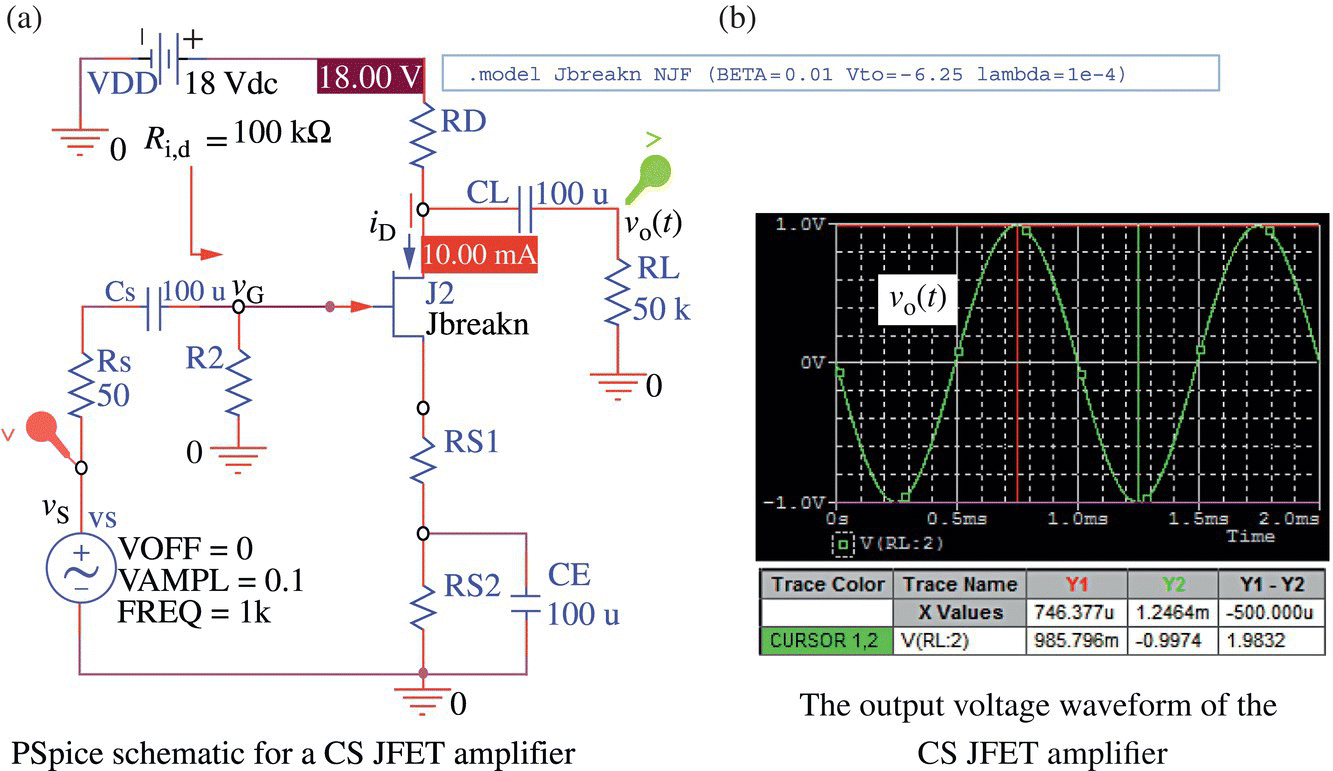
Figure P4.18 A CS JFET circuit and its output voltage waveform (“elec04p18.opj”).
- Referring to Figure P4.18(a), perform the PSpice simulation of the designed CS JFET amplifier with Time Domain analysis to see the output voltage vo(t) to an AC input vs(t) = Vsm sin (2000πt) (with Vsm = 0.1 V) for t = 0–2 ms (with the maximum step size 1 us) as shown in Figure P4.18(b). Find the voltage gain and check if it agrees with the analysis result (obtained in (a)) and satisfies the design specification Av,d = −10. Note that BETA, one of the PSpice model parameters for JFET, must be given as Kp/2.
(Note) If the MATLAB function ‘
FET_CS_design()’ turns out to work for this problem, it implies that the function can be used to design CS JFET amplifiers as well as CS MOSFET amplifiers.
- Considering the load resistance RL = 50 kΩ, determine such resistor values that the voltage gain Av,d = −10 and input resistance Ri,d = 100 kΩ can be achieved with the operating point located near Q1 = (VDS,Q,ID,Q) = (6 V,10 mA). Analyze the designed circuit with source/load resistance Rs = 50 Ω/RL = 50 kΩ to find the voltage gain Av. Is it close to Av,d = −10?
- 4.19 Design of CS MOSFET Amplifier Circuit
Consider the CS MOSFET amplifier circuit of Figure P4.19(a) where the conduction parameter, threshold voltage, and CLM parameter of the MOSFET (IRF150) are KP = KPW/L = 20.53μ × 0.3/2μ = 3.08 A/V2, Vt = 2.831 V, and λ = 2.2 mV−1, respectively.
- Considering the load resistance RL = 50 kΩ, determine such resistor values that the voltage gain Av,d = −10 and input resistance Ri,d = 100 kΩ can be achieved with the operating point located near Q1 = (VDS,Q, ID,Q) = (18/7 V, 1 mA). Analyze the designed circuit with source/load resistance Rs = 50 Ω/RL = 50 kΩ to find the voltage gain Av. Is it close to Av,d = −10?
(Hint) Complete and run the above MATLAB script “elec04p19.m”.
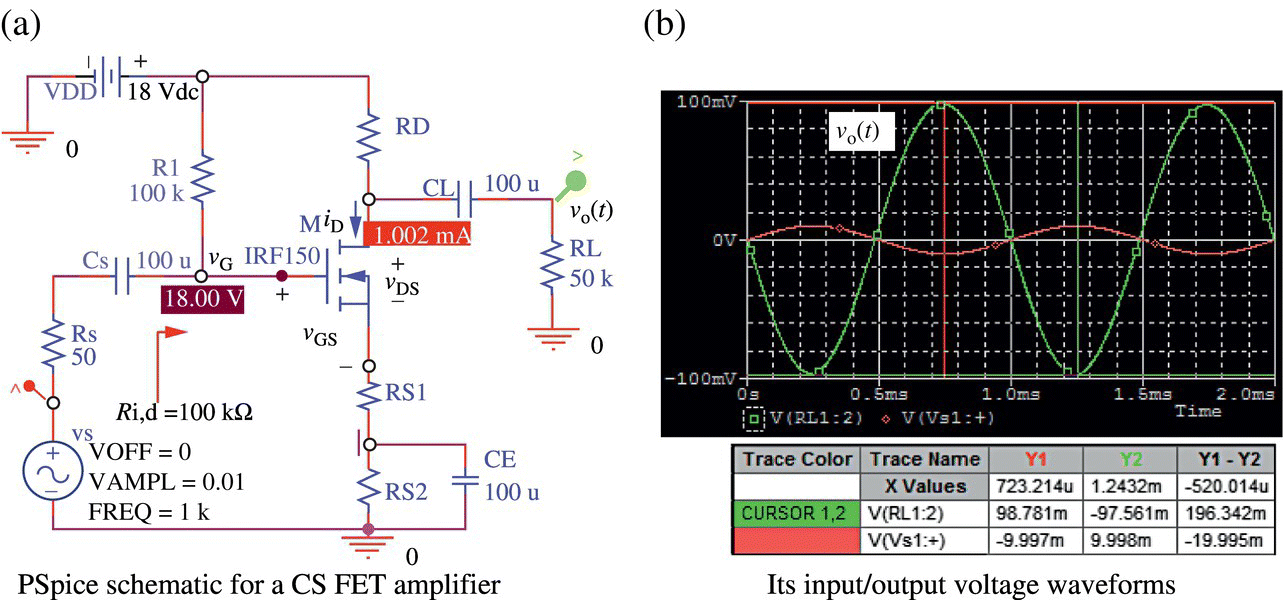
Figure P4.19 A CS MOSFET circuit and its input/output voltage waveforms (“elec04p19.opj”).
- Referring to Figure P4.19(a), perform the PSpice simulation of the designed CS FET amplifier with Time Domain analysis to see the output voltage vo(t) to an AC input vs(t) = Vsm sin (2000πt) (with Vsm = 0.01 V) for t = 0~2 ms (with the maximum step size 1 μs) as shown in Figure P4.19(b). Find the voltage gain and check if it agrees with the analysis result (obtained in (a)) and satisfies the design specification Av,d = −10.
- Considering the load resistance RL = 50 kΩ, determine such resistor values that the voltage gain Av,d = −10 and input resistance Ri,d = 100 kΩ can be achieved with the operating point located near Q1 = (VDS,Q, ID,Q) = (18/7 V, 1 mA). Analyze the designed circuit with source/load resistance Rs = 50 Ω/RL = 50 kΩ to find the voltage gain Av. Is it close to Av,d = −10?
- 4.20 Design of CS MOSFET Amplifier Circuit
Consider the CS MOSFET amplifier circuit of Figure 4.36(a) where the conduction parameter, threshold voltage, and CLM parameter of the MOSFET (IRF150) are KP = KPW/L = 20.53μ × 0.3/2μ = 3.08 A/V2, Vt = 2.831 V, and λ = 0.0075 mV−1, respectively. Let us see how the location of (static) operating point depending on the design constants such as ID,Q and VDS,Q affects the distortion of the output voltage waveform (to an AC input vs(t)=Vsmsin(2000πt) with Vsm= 0.3 V) caused by the (dynamic) operating point infringing on the ohmic or cutoff region.
- In Section 4.3, a CS FET amplifier (Figure 4.36(a)) with the static operating point at Qa = (VDS,Q, ID,Q) = (18/3 V, 0.3 mA) was designed so that it could have the voltage gain Av,d = −20 and input resistance Ri,d = 100 kΩ. Perform the PSpice simulation with Time Domain analysis to see the output voltage vo(t) to an AC input vs(t) = Vsm sin (2000πt) (with Vsm = 0.3 V) as shown in Figure P4.20(a). If vo(t) has any distortion, could it be predicted from the MATLAB analysis?
- Determine the resistor values of the CS FET amplifier with the static operating point at Qb = (VDS,Q, ID,Q) = (6 V, 3 mA) so that it can have the same voltage gain Av,d = −20 and input resistance Ri,d = 100 kΩ with ID,Q increased from 0.3 mA to 3 mA. Use the MATLAB function ‘
FET_CS_analysis()’ to analyze the designed circuit with the source/load resistance of Rs = 50 Ω/RL = 50 kΩ. Does it give you any warning message of ohmic/cutoff regions to be trespassed on? Perform the PSpice simulation with Time Domain analysis to see the output voltage to an AC input vs(t) = Vsm sin (2000πt) (with Vsm = 0.3 V) as shown in Figure P4.20(b). Does any distortion of vo(t) agree with the warning message given by the MATLAB analysis? - Determine the resistor values of the CS FET amplifier with the static operating point at Qc = (VDS,Q, ID,Q) = (8 V, 3 mA) so that it can have the same voltage gain Av,d = −20 and input resistance Ri,d = 100 kΩ with VDS,Q increased from 6 V to 8 V. Use the MATLAB function ‘
FET_CS_analysis()’ to analyze the designed circuit with the source/load resistance of Rs = 50 Ω/RL = 50 kΩ. Does it give you any warning message of ohmic/cutoff regions to be trespassed on? Perform the PSpice simulation with Time Domain analysis to see the output voltage to an AC input vs(t) = Vsm sin (2000πt) (with Vsm = 0.3 V) as shown in Figure P4.20(c). - Determine the resistor values of the CS FET amplifier with the static operating point at Qd = (VDS,Q, ID,Q) = (4.5 V, 3 mA) so that it can have the same voltage gain Av,d = −20 and input resistance Ri,d = 100 kΩ with VDS,Q decreased from 6 V to 4.5 V. Use the MATLAB function ‘
FET_CS_analysis()’ to analyze the designed circuit with the source/load resistance of Rs = 50 Ω/RL = 50 kΩ. Does it give you any warning message of ohmic/cutoff regions to be trespassed on? Perform the PSpice simulation with Time Domain analysis to see the output voltage to an AC input vs(t) = Vsm sin (2000πt) (with Vsm = 0.3 V) as shown in Figure P4.20(d). Does any distortion of vo(t) agree with the warning message given by the MATLAB analysis? - Determine the resistor values of the CS FET amplifier with the static operating point at Qe = (VDS,Q, ID,Q) = (6 V, 20 mA) so that it can have the same voltage gain Av,d = −20 and input resistance Ri,d = 100 kΩ with ID,Q increased from 0.3 mA to 20 mA. Use the MATLAB function ‘
FET_CS_analysis()’ to analyze the designed circuit with the source/load resistance of Rs = 50 Ω/RL = 50 kΩ. Does it give you any warning message of ohmic/cutoff regions to be trespassed on? Perform the PSpice simulation with Time Domain analysis to see the output voltage to an AC input vs(t) = Vsm sin (2000πt) (with Vsm = 0.3 V) as shown in Figure P4.20(e). Does any distortion of vo(t) agree with the warning message given by the MATLAB analysis?

Figure P4.20 Output voltage waveforms of CS FET amplifier with different resistances (“elec04p20.opj”).
- Frequency Response of an FET Cascode Amplifier
Consider the FET cascode amplifier with PSpice schematic and simulation result on the frequency response in Figure P4.21(a) and (b), respectively, where VDD = 12 V, Rs = 50 Ω, Cs = 100 μF, R1 = 200 kΩ, R2 = 100 kΩ, R3 = 100 kΩ, RS = 1 kΩ, CS = 100 μF, CG = 100 μF, RD = 3 kΩ, CL = 100 μF, RL = 100 kΩ, CLL = 0.1 nF, and the parameters of the enhancement type NMOSs are Kp = 10 mA/V2, Vt = 1 V, and λ = 10−4 V−1, Cgs0 = 10 pF, Cgd0 = 1 pF, and Cds = 0 F.
- Complete the following MATLAB function ‘
FET_cascode_DC_analysis()’, which performs the DC analysis to determine the node voltages and drain currents at the operating point.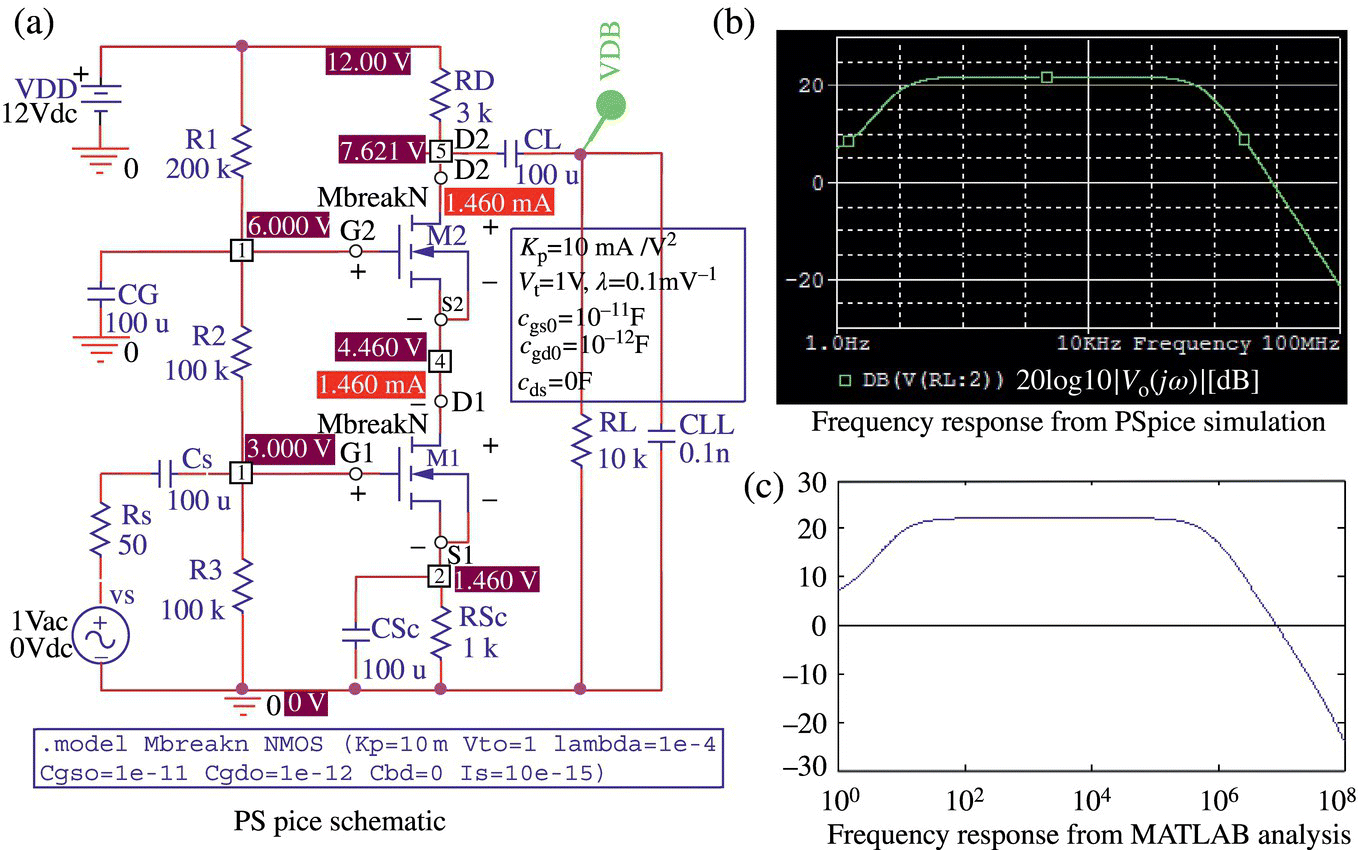
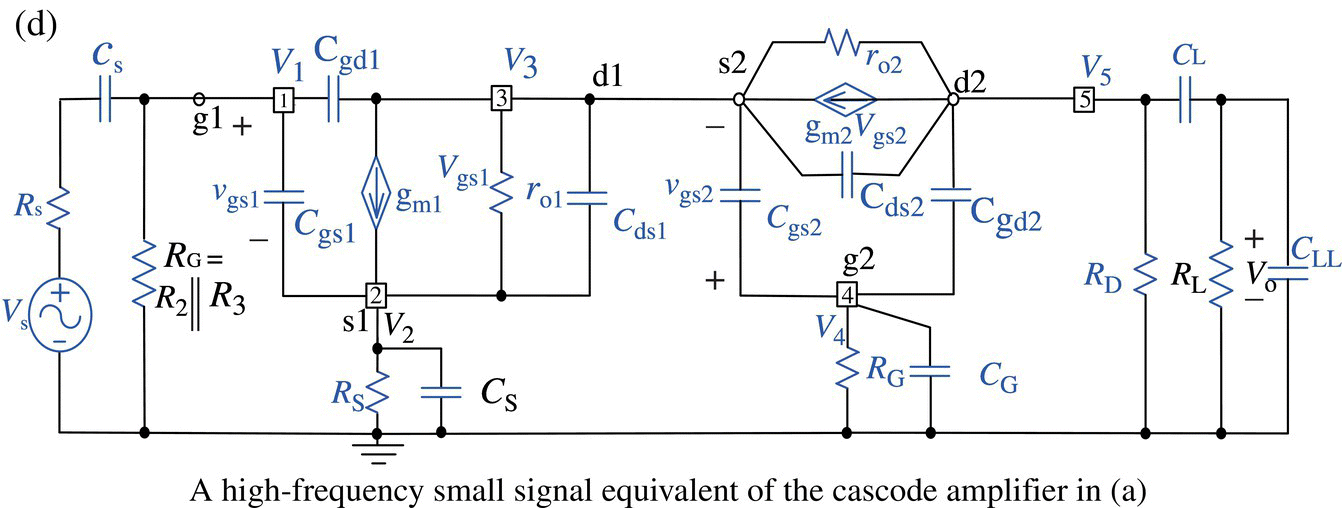
Figure P4.21 Cascode amplifier and its frequency response from PSpice and MATLAB (“elec04p21.opj”).
- Complete the following MATLAB function ‘
FET_cascode_xfer_ftn()’, which solves a set of 3, 4, or 5 node equations for the high‐frequency small‐signal equivalent (Figure P4.21(d)) depending on whether or not nodes 2/3 are AC grounded via capacitors CSC/CG, respectively, to find the transfer function G(s) = Vo(s)/Vs(s) of the cascade amplifier. - Run the following MATLAB script “elec04p21.m” to perform the DC analysis (using ‘
FET_cascode_DC_analysis()’), then based on the DC analysis result, use ‘FET_cascode_xfer_ftn()’ to find the transfer function G(s), and plot the frequency response magnitude 20log10|G(jω)| [dB] of the cascade amplifier versus f = 1~100 MHz as shown in Figure P4.21(c). - Perform the PSpice simulation (with AC Sweep analysis) to get the frequency response magnitude curve as depicted in Figure P4.21(b). Is the Bias Point analysis result (obtained as a by‐product) close to the DC analysis result obtained by using ‘
FET_cascode_DC_analysis()’ in (c)?
- Complete the following MATLAB function ‘
- Time Response of an FET Inverter with another Inverter as a Load
Consider the FET inverter in Figure P4.22(a) where VDD = 12 V, RD = 10 kΩ, RD1 = 10 kΩ, and the FET parameters are Kp = 5 mA/V2, Vt = 1 V, λ = 10−4 V−1, Cgs0 = 10 fF, Cgd0 = 1 fF, Cbd0 = 10 fF or 20 fF for M1, and Kp = 5 mA/V2, Vt = 1 V, λ = 10−4 V−1, Cgs0 = 10 fF, Cgd0 = 1 fF, Cbd0 = 10 fF for M2.
Figure P4.22(b1) and (b2) shows the input/output voltage waveforms obtained from PSpice simulation, each with Cbd = 10 fF and 20 fF for M1, respectively. Referring to Section 4.5 and Figure P4.22(b1‐b2), explain how a larger value of Cbd makes a longer time constant of vo1 during its rising period.
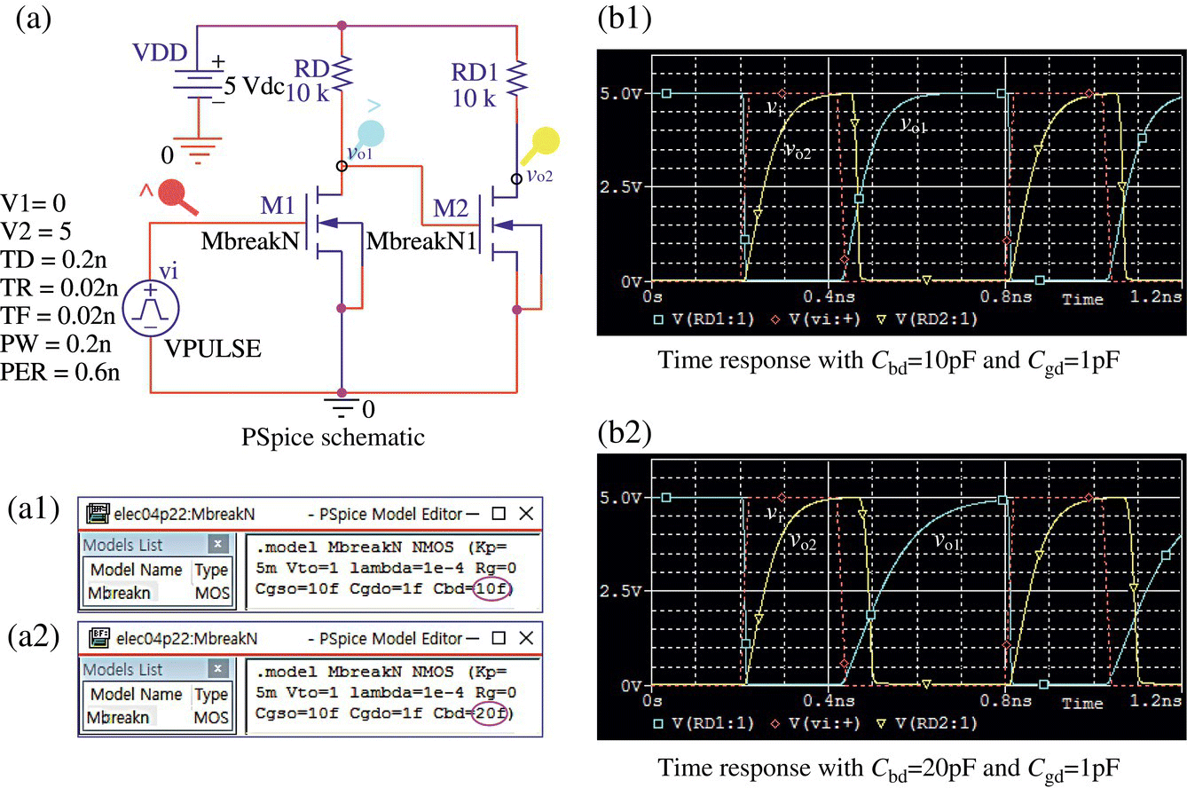
Figure P4.22 FET inverter with another inverter as a load and its time responses from PSpice (“elec04p22.opj”).