6
Analog Filter
This chapter discusses how to design and realize analog filters in the form of passive filters and active filters.
6.1 Analog Filter Design
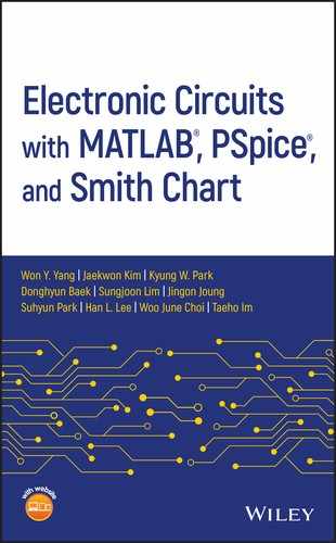
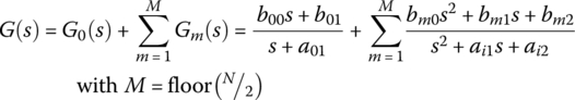
Figure 6.1(a)‐(d) shows typical low‐pass/band‐pass/band‐stop/high‐pass filter (LPF/BPF/BSF/HPF) specifications on their log magnitude, 20log10|G(jω)| [dB], of frequency response. The filter specification can be described as follows:
where ωp, ωs, Rp, and As are referred to as the passband edge frequency, the stopband edge frequency, the passband ripple, and the stopband attenuation, respectively. The most commonly used analog filter design techniques are the Butterworth, Chebyshev I, II, and elliptic ones ([K-2], Chapter 8). MATLAB has the built‐in functions ‘butt()’, ‘cheby1()’, ‘cheby2()’, and ‘ellip()’ for designing the four types of analog/digital filter. As summarized below, ‘butt()’ needs the 3 dB cutoff frequency while ‘cheby1()’ and ‘ellip()’ take the critical passband edge frequency and ‘cheby2()’ the critical stopband edge frequency as one of their input arguments. The parametric frequencies together with the filter order can be predetermined using ‘buttord()’, ‘cheb1ord()’, ‘cheb2ord()’, and ‘ellipord()’. The frequency input argument should be given in two‐dimensional vector for designing BPF or BSF. Also for HPF/BSF, the string 'high'/'stop' should be given as an optional input argument together with 's' for analog filter design.
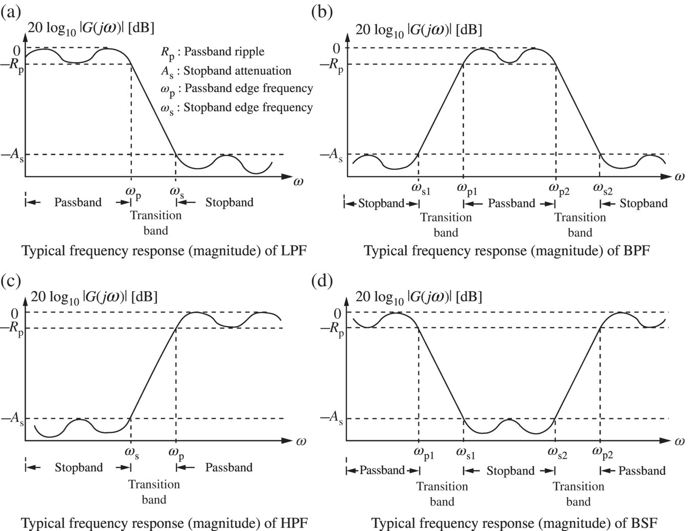
Figure 6.1 Specifications on the log magnitude of analog filter frequency response.
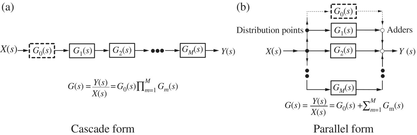
Figure 6.2 Two realizations of analog filter (system or transfer function).
A designed filter transfer function of order N is often factored into the sum or product of SOSs (second‐order sections) called biquads (possibly with an additional first‐order section in the case of an odd filter order) as
and then realized in cascade or parallel form, respectively, as depicted in Figure 6.2.
Rather than reviewing the design procedures, let us use the MATLAB functions to design a Butterworth low‐pass filter, a Chebyshev I band‐pass filter, a Chebyshev II BSF, and elliptic HPF in the following example.
6.2 Passive Filter
6.2.1 Low‐pass Filter (LPF)
6.2.1.1 Series LR Circuit
Figure 6.4(a) shows a series LR circuit where the voltage vR(t) across the resistor R is taken as the output to the input voltage source vi(t). With VR(s) = ![]() {vR(t)} and Vi(s)=
{vR(t)} and Vi(s)=![]() {vi(t)}, its input‐output relationship can be described by the transfer function and the frequency response as
{vi(t)}, its input‐output relationship can be described by the transfer function and the frequency response as
Figure 6.3 Frequency response magnitude curves of the filters designed in Example 8.7.

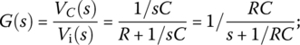
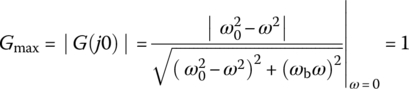
Since the magnitude |G(jω)| of this frequency response becomes smaller as the frequency ω gets higher as depicted in Figure 6.4(b), the circuit is a lowpass filter (LPF) that prefers to have low‐frequency components in its output. Noting that |G(jω)| achieves the maximum Gmax = G(j0) = 1 at ω = 0, we can find the cutoff frequency ωc at which it equals ![]() as
as
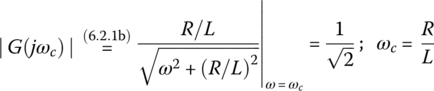
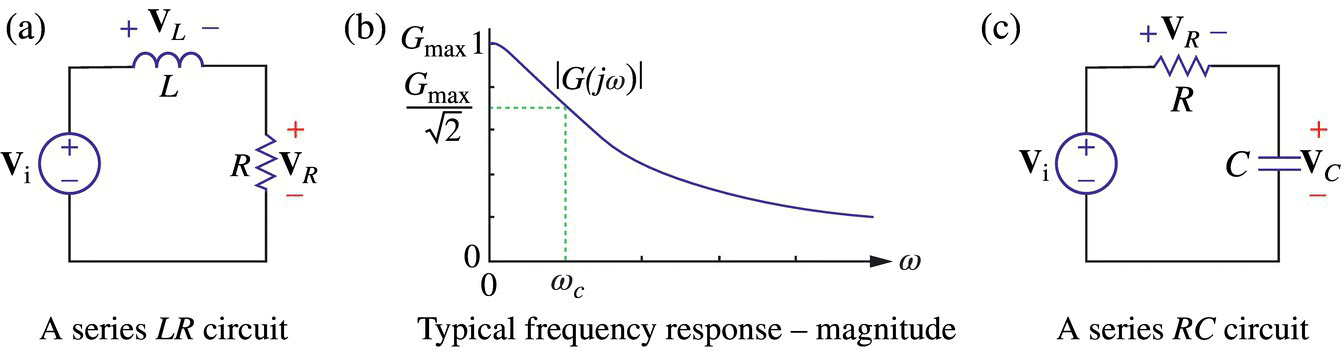
Figure 6.4 Low‐pass filters and their typical frequency response.
The cutoff frequency has a physical meaning as the boundary frequency between the passband and the stopband. Why do we use ![]() for its definition? In most cases, the transfer function and the frequency response is the ratio of output and input voltages/currents in s‐frequency domain. Since an electric power is proportional to the squared voltage and current, the ratio of
for its definition? In most cases, the transfer function and the frequency response is the ratio of output and input voltages/currents in s‐frequency domain. Since an electric power is proportional to the squared voltage and current, the ratio of ![]() between voltages/currents corresponds to the ratio of 1/2 between powers. For this reason, the cutoff frequency is also referred to as a half‐power frequency or a 3dB frequency on account of that 10log10(1/2) = −3 [dB]. In the case of LPF with cutoff frequency ωc like this circuit, the passband is the range of frequency [0, ωc] and its width is the bandwidth, where the bandwidth means the width of the range of frequency components that pass the filter better than others.
between voltages/currents corresponds to the ratio of 1/2 between powers. For this reason, the cutoff frequency is also referred to as a half‐power frequency or a 3dB frequency on account of that 10log10(1/2) = −3 [dB]. In the case of LPF with cutoff frequency ωc like this circuit, the passband is the range of frequency [0, ωc] and its width is the bandwidth, where the bandwidth means the width of the range of frequency components that pass the filter better than others.
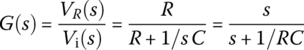
6.2.1.2 Series RC Circuit
Figure 6.4(c) shows a series RC circuit where the voltage vC(t) across the capacitor C is taken as the output to the input voltage source vi(t). With VC(s)=![]() {vC(t)} and Vi(s)=
{vC(t)} and Vi(s)=![]() {vi(t)}, its input‐output relationship can be described by the transfer function and the frequency response as
{vi(t)}, its input‐output relationship can be described by the transfer function and the frequency response as

Everything is the same with the series LR circuit in Figure 6.4(a) except for that the cutoff frequency is
6.2.2 High‐pass Filter (HPF)
6.2.2.1 Series CR Circuit
Figure 6.5(a) shows a series CR circuit where the voltage vR(t) across the resistor R is taken as the output to the input voltage source vi(t). Its input‐output relationship can be described by the transfer function and the frequency response as
Since the magnitude |G(jω)| of this frequency response becomes larger as the frequency ω gets higher as depicted in Figure 6.5(b), the circuit is a highpass filter (HPF) that prefers to have high‐frequency components in its output. Noting that |G(jω)| achieves the maximum Gmax=G(j∞)=1 at ω=∞, we can find the cutoff frequency ωc at which it equals ![]() as
as
6.2.2.2 Series RL Circuit
Figure 6.5(c) shows a series RL circuit where the voltage vL(t) across the inductor L is taken as the output to the input voltage source vi(t). Its input‐output relationship can be described by the transfer function and the frequency response as
Everything is the same with the series CR circuit in Figure 6.5(a) except for that the cutoff frequency is
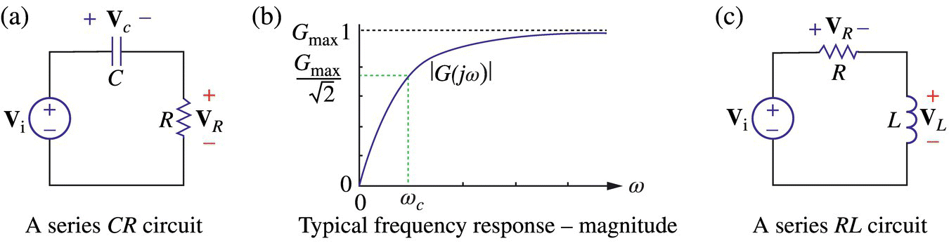
Figure 6.5 High‐pass filters and their typical frequency response.
6.2.3 Band‐pass Filter (BPF)
6.2.3.1 Series Resistor, an Inductor, and a Capacitor (RLC) Circuit and Series Resonance
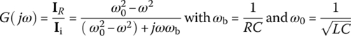
Let us consider the series resistor, an inductor, and a capacitor (RLC) circuit of Figure 6.6(a) in which the voltage vR(t) across the resistor R is taken as the output to the input voltage source vi(t). Its input‐output relationship can be described by the transfer function and the frequency response as

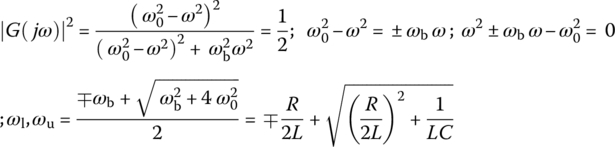
Referring to the typical magnitude curve of the frequency response of a bandpass filter (BPF) shown in Figure 6.6(b), we can find the maximum of the magnitude, |G(jω)|, of the frequency response by setting the derivative of its square |G(jω)|2 w.r.t. frequency ω to zero as
This yields the peak or center frequency
at which the frequency response achieves the maximum magnitude as
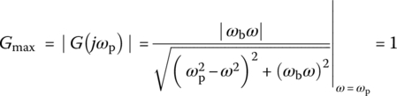
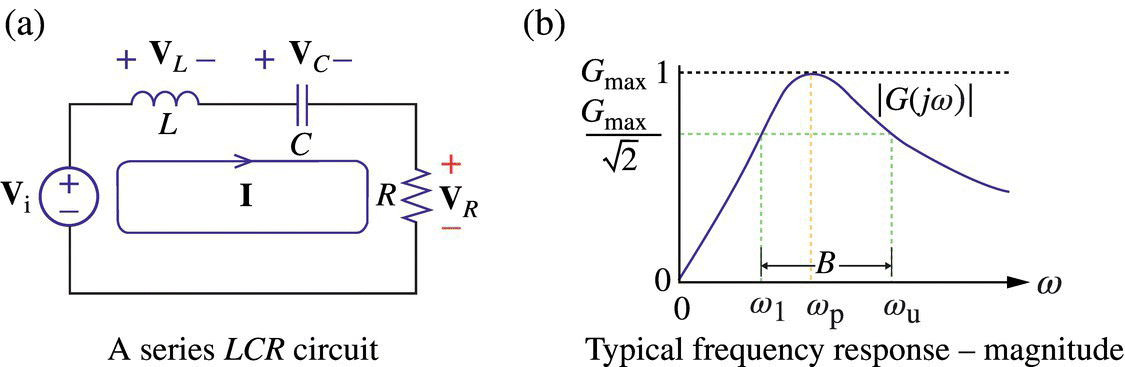
Figure 6.6 A band‐pass filter (BPF) and its typical frequency response.
This frequency happens to coincide with the resonant frequency ωr at which the frequency response is real so that the input and the output are in phase at that frequency. We can also find the lower and upper 3dB frequencies at which the magnitude |G(jω)| of this frequency response is ![]() as
as
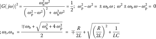
Multiplying these two 3 dB frequencies and taking the square root yields
This implies that the peak frequency ωp is the geometrical mean of two 3 dB frequencies ωl and ωu and also the arithmetical mean of their logarithmic values that is at the midpoint between the two 3 dB frequency points on the log‐frequency (log ω) axis. That is why ωp is also called the center frequency. The frequency band between the two 3 dB frequencies ωl and ωu is the passband and its width is the bandwidth:
Note that the bandwidth for a BPF is the width of the range of frequency components that pass the filter better than others.
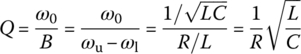
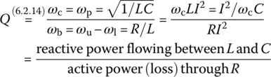
For a BPF, we define the quality factor or selectivity (sharpness) as
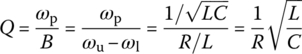
This quality factor is referred to as the selectivity since it is a measure of how selectively the filter responds to the peak frequency and frequencies near it within the passband, discriminating against frequencies outside the passband. It is also referred to as the sharpness in the sense that it describes how sharp the magnitude curve of the frequency response is around the peak frequency. It coincides with the voltage magnification ratio, that is, the ratio of the magnitude of the voltage across the inductor or the capacitor to that of the input voltage at peak frequency as

which may be greater than unity. Isn't it interesting that the voltages across some components of a circuit can be higher than the applied voltage?
Now, let us see the following example showing how to determine the parameters of a series RLC circuit so that it can function as a BPF satisfying a design specification on the passband.
6.2.3.2 Parallel RLC Circuit and Parallel Resonance
Let us consider the parallel RLC circuit of Figure 6.7(a) in which the current iR(t) through the resistor R is taken as the output to the input current source ii(t). Its input‐output relationship can be described by the transfer function and the frequency response as
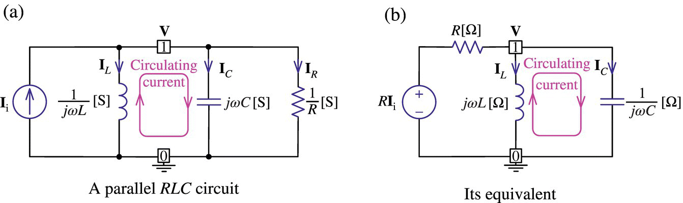
Figure 6.7 A parallel resistor, an inductor, and a capacitor (RLC) circuit and its equivalent.

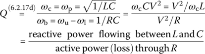
Since this frequency response is the same as that, Eq. (6.2.9b), of the series RLC circuit in Figure 6.6(a) except for ωb, we can obtain the peak or center frequency, the upper/lower 3dB frequencies, the bandwidth, and the quality factor as follows:
The peak frequency happens to be coinciding with the resonant frequency ωr in the sense that the frequency response is real so that the input and the output are in phase at that frequency. The quality factor coincides with the current magnification ratio, that is, the ratio of the amplitude of the current through the inductor or the capacitor to that of the input current at resonant frequency as

which may be greater than unity. How strange it is that the currents through some components of a circuit can be larger than the applied current!
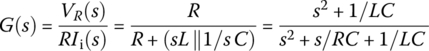
Let us now consider RLC circuit of Figure 6.7(b) in which the voltage across L‖C (the parallel combination of L and C) is taken as the output to the input voltage source RIi. We can use the voltage divider rule to obtain the transfer function as
This is the same as Eq. (6.2.16a), which is the transfer function of the parallel RLC circuit of Figure 6.7(a). In fact, the circuit of Figure 6.7(b) is obtained by transforming the current source Ii in parallel with R into a voltage source RIi in series with R in the circuit of Figure 6.7(a).
6.2.4 Band‐stop Filter (BSF)
6.2.4.1 Series RLC Circuit
Let us consider the series RLC circuit of Figure 6.9(a) in which the voltage vLC(t) across the series combination of L and C is taken as the output to the input voltage source vi(t). Its input‐output relationship can be described by the transfer function and the frequency response as
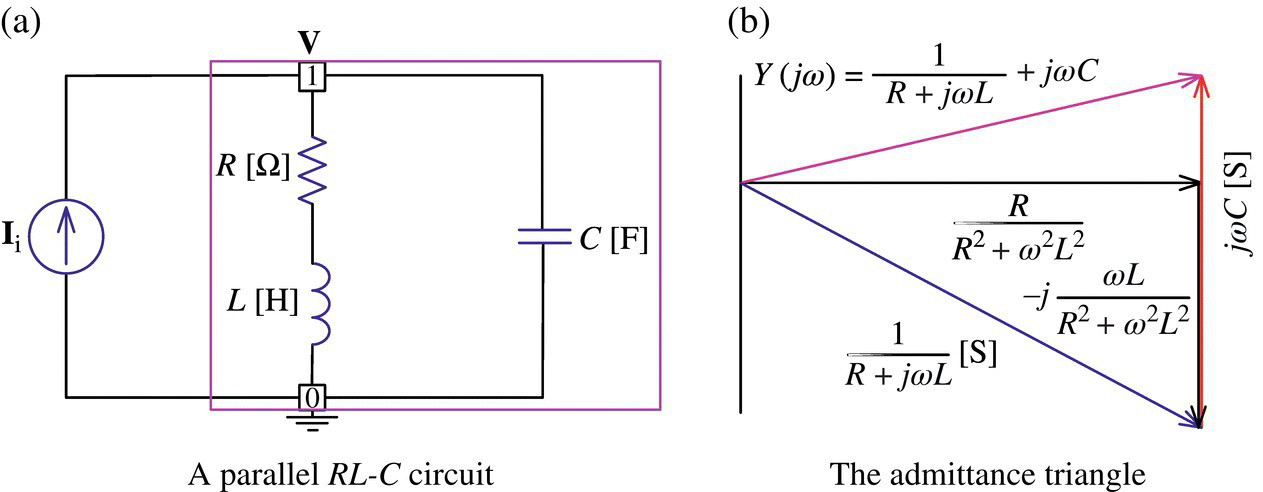
Figure 6.8 A practical parallel resonant circuit and its admittance triangle.
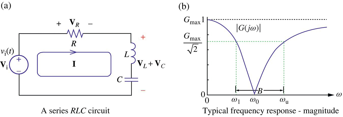
Figure 6.9 A band‐stop filter (BSF) and its typical frequency response.


Referring to the typical magnitude curve of the frequency response of a BSF shown in Figure 6.9(b), we can find the minimum of the magnitude of the frequency response by setting the derivative of its square w.r.t. the frequency ω to zero as
This yields the notch, rejection, or center frequency
at which the frequency response achieves the minimum magnitude as
(Note) It is hoped that the readers will enjoy the dual sense of ωr, as the resonant frequency of BPF or the rejection (notch) frequency of BSF (depending on the context), rather than being confused.
Noting that the magnitude of the frequency response achieves its maximum of unity at another extremum frequency ω = 0 or ω = ∞ as
we can find the lower and upper 3 dB frequencies at which the magnitude |G(jω)| of this frequency response is ![]() as
as
Multiplying these two 3 dB frequencies and taking the square root yields
This implies that the notch frequency ωr is the geometrical mean of two 3 dB frequencies ωl and ωu and also the arithmetical mean of their logarithmic values that is at the midpoint between the two 3 dB frequency points on the log‐frequency (log ω) axis. The band of frequencies between the two 3 dB frequencies ωl and ωu is the stopband and its width is the bandwidth:
Note that the bandwidth for a BSF is the width of the range of frequency components that are relatively more attenuated or rejected by the filter than other frequencies.
For a BSF, we define the quality factor or selectivity (sharpness) as
This quality factor is referred to as the selectivity since it is a measure of how selectively the filter rejects the notch frequency and frequencies near it within the stopband, favoring frequencies outside the stopband. It is also referred to as the sharpness in the sense that it describes how sharp the magnitude curve of the frequency response is around the rejection or notch frequency.
6.2.4.2 Parallel RLC Circuit
Let us consider the parallel RLC circuit of Figure 6.10(a) in which the current iL(t) + iC(t) through the parallel combination of L and C is taken as the output to the input current source ii(t). Its input‐output relationship can be described by the transfer function and the frequency response as


Figure 6.10 Band‐stop filter (BSF).
Since this frequency response is the same as that, Eq. (6.2.19b), of the series RLC circuit in Figure 6.9(a) except for ωb, we have the same results for the notch or rejection or center frequency, the upper/lower 3 dB frequencies, the bandwidth, and the quality factor.
Let us now consider the RLC circuit of Figure 6.10(b) in which the voltage across R is taken as the output to the input voltage source RIi. We can use the voltage divider rule to obtain the transfer function as
This is exactly the same as Eq. (6.2.24a), which is the transfer function of the parallel RLC circuit of Figure 6.10(a). In fact, this circuit is obtained by transforming the current source Ii in parallel with R into a voltage source RIi in series with R in the circuit of Figure 6.10(a).
6.2.5 Quality Factor
In the previous sections, the quality factors for series and parallel RLC circuits were defined as the ratio of the center frequency ωc to the bandwidth B= ωu ‐ ωl where ωu and ωl are the upper and lower 3 dB frequencies, respectively:
Note that the quality factor Q of a circuit can be viewed as the ratio of the reactive power (i.e. the maximum power stored in L or C) to the active power of the circuit.
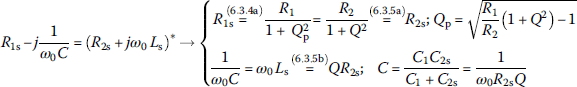
Now, let us consider the quality factor of an individual reactive element L or C at the center frequency ωc of the circuit containing the element. It depends on whether the element is modeled as a series or parallel combination with its loss (parasitic) resistance:
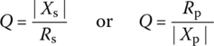
where
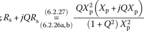

Note that these equivalence conditions between the series and parallel combination models of a reactive element are valid only at a certain frequency since the reactances are frequency dependent. The series‐to‐parallel and parallel‐to‐series conversion processes of L‐R and C‐R circuits have been cast into the following MATLAB functions:
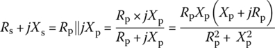
Now, let us consider the (loaded) quality factor [L-1] QLD of a series RLC circuit with the source resistance Rs and the load resistance RL as shown in Figure 6.12(a). Noting that the circuit is a series connection of (Rs+R+RL)‐L‐C, we can use Eq. (6.2.25a) to write the loaded quality factor QLD as
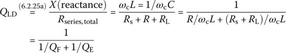
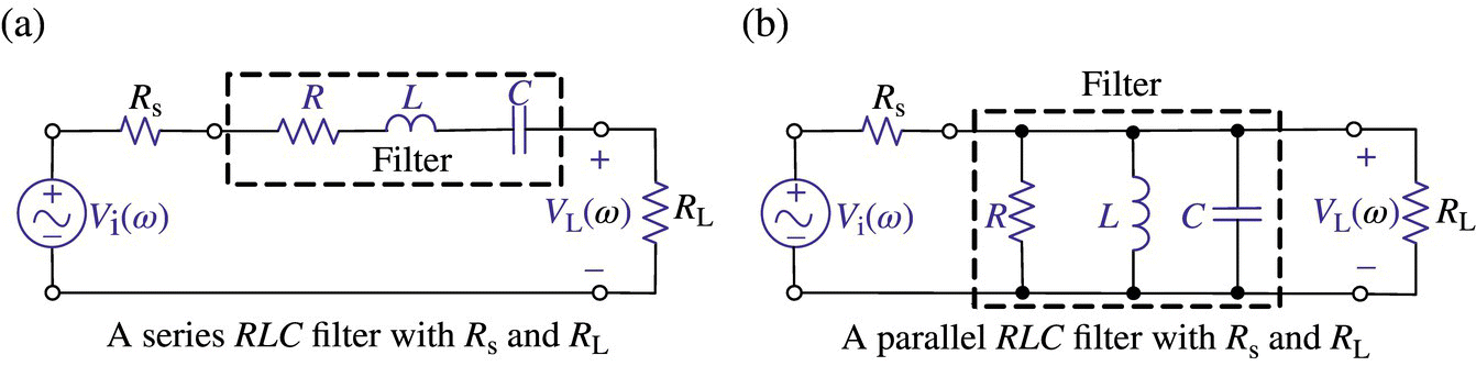
Figure 6.12 Circuits for the definitions of the loaded quality factor QLD.
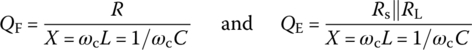
where the filter quality factor QF and the external quality factor QE are as follows:
Likewise, the loaded quality factor QLD of a parallel RLC circuit with the source resistance Rs and the load resistance RL as shown in Figure 6.12(b) can be written as
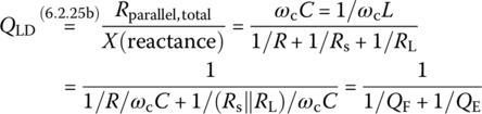
where the filter quality factor QF and the external quality factor QE are as follows:
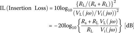
6.2.6 Insertion Loss
When designing a filter to be inserted in a telecommunication system as can be modeled by, say, Figure 6.12(a) or (b), it is important to consider the insertion loss (IL) of the filter, which is defined as the ratio of the power (delivered to the load without the filter) to the power (delivered to the load with the filter inserted):
6.2.7 Frequency Scaling and Transformation
Note the following remarks on frequency scaling and frequency transformation:
Table 6.1 Frequency transformation.
| Frequency transformations | MATLAB function |
| LPF with cutoff frequency ωc: s → s/ωc(6.2.36a) This corresponds to substituting |
lp2lp() |
| HPF with cutoff frequency ωc: s → ωc/s(6.2.37a) This corresponds to substituting |
lp2hp() |
BPF with upper/lower cutoff frequencies ωu/ωl:  (6.2.38a) (6.2.38a)This corresponds to substituting ( 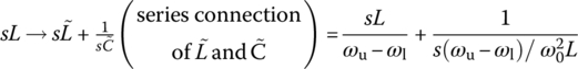 (6.2.38b) (6.2.38b)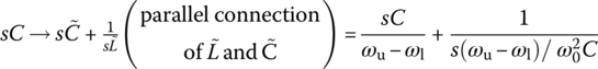 (6.2.38c) (6.2.38c) |
lp2bp() |
| BSF with upper/lower cutoff frequencies ωu/ωl: This corresponds to substituting ( 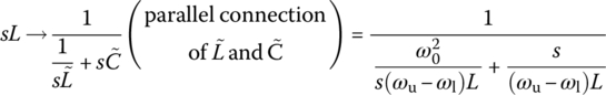 (6.2.39b) (6.2.39b)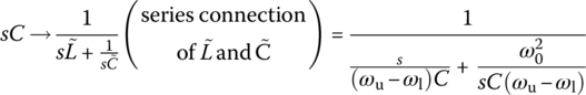 (6.2.39c) (6.2.39c) |
lp2bs() |
6.3 Passive Filter Realization
6.3.1 LC Ladder
Figure 6.14.1(a) and (b) shows the П‐type and T‐type of LC ladder that can be used to realize a prototype LPF where the values of L's, C's, and RL are listed as {g1, g2, … } in Tables 5.2 (Butterworth), 5.3 (linear‐phase), 5.4 (Chebyshev 3 dB), and 5.5 (Chebyshev 0.5 dB) of [L-1] and can also be determined by using the following MATLAB function ‘LPF_ladder_coef()’.
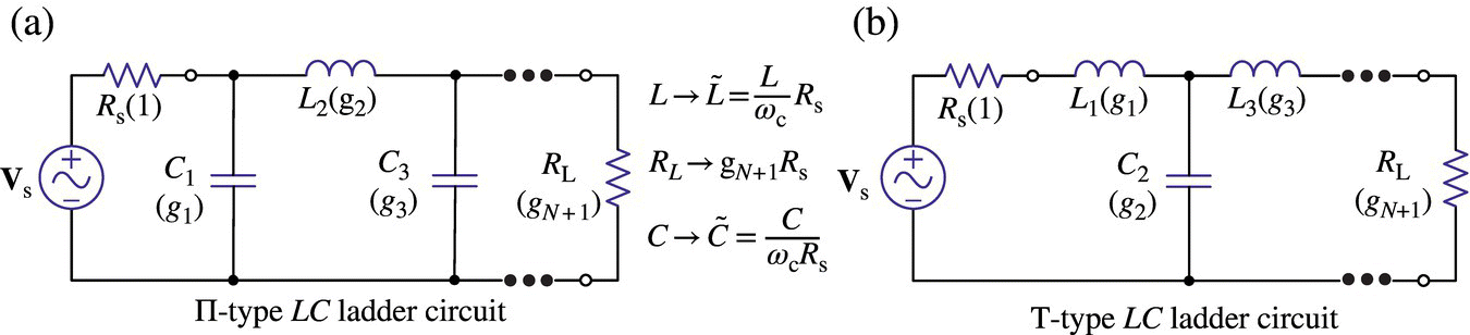
Figure 6.14.1 LC ladders realizing low‐pass filter (LPF).
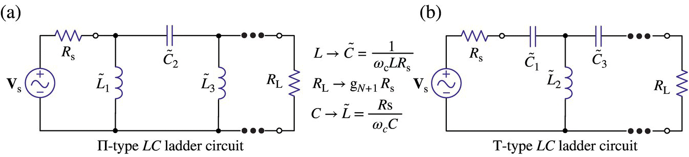
The formulas listed in Table 6.1 can be used to magnitude/frequency scale the LC filter prototypes to make them realize LPF/HPF/BPF/BSF with unnormalized cutoff frequency as depicted in Figures 6.14.1‐6.14.4.
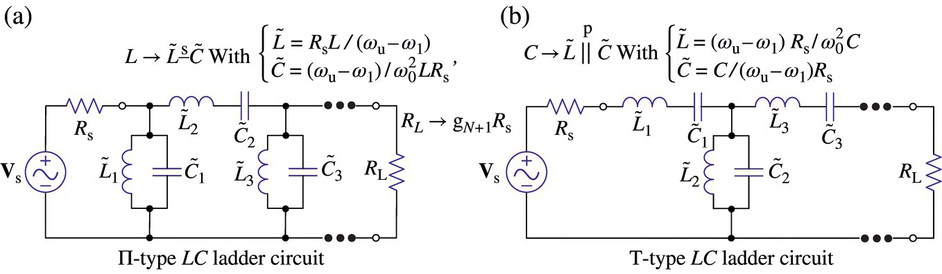
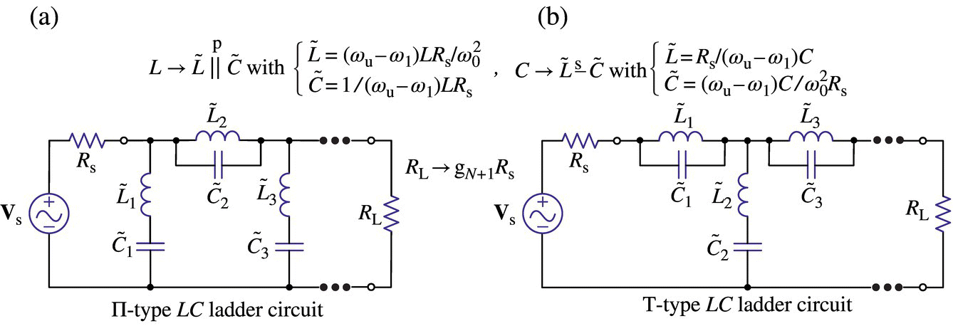
Figure 6.14.4 LC ladders realizing BSF.
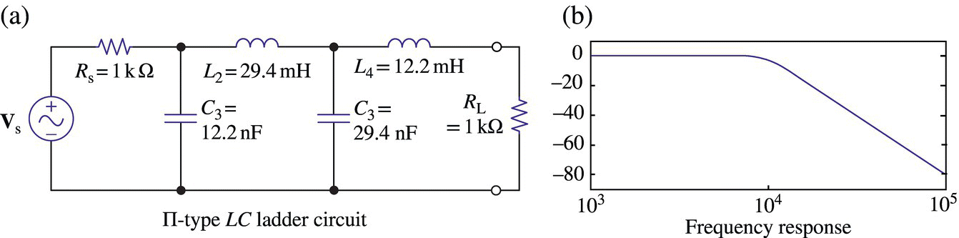
Figure 6.16 Fourth‐order Butterworth LPF realized with a П‐type LC ladder and its frequency response.
6.3.2 L‐Type Impedance Matcher
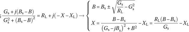
Figure 6.18 shows two L‐types of LC filters (with Zk = jXk = jωLk or Zk = jXk = 1/jωCk) that can be used to accomplish the impedance matching condition [Y-1], (6.38) ![]() (*: complex conjugate) between the source impedance Zs = Rs + jXs and load impedance ZL = RL + jXL. The impedance matching condition for maximum power transfer of L1‐type filter (Figure 6.18(a)) can be written as
(*: complex conjugate) between the source impedance Zs = Rs + jXs and load impedance ZL = RL + jXL. The impedance matching condition for maximum power transfer of L1‐type filter (Figure 6.18(a)) can be written as
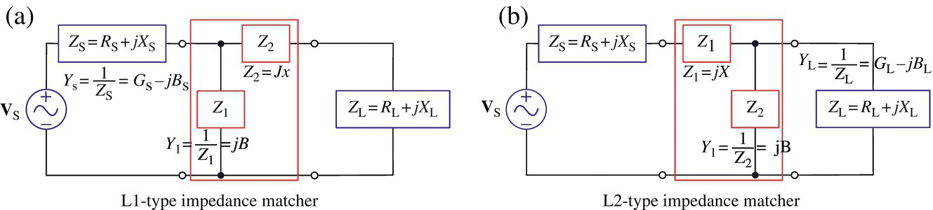
Figure 6.18 L‐type impedance matchers.
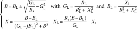
Likewise, noting that the structure of L2‐type filter (Figure 6.18(b)) is just like the reverse of L1‐type filter with Zs and ZL switched, the impedance matching condition of L2‐type filter can be written as
The above MATLAB function ‘imp_matcher_L()’ can be used to find possible L‐type filter(s) for impedance matching between given source/load impedances. Note that the function without the fourth input argument ‘type’ returns all possible L‐type LC filters while with type = 1/2, it returns just L1‐/L2‐type LC filter(s).

Figure 6.19 L‐type filters used for impedance matching in Example 6.12.
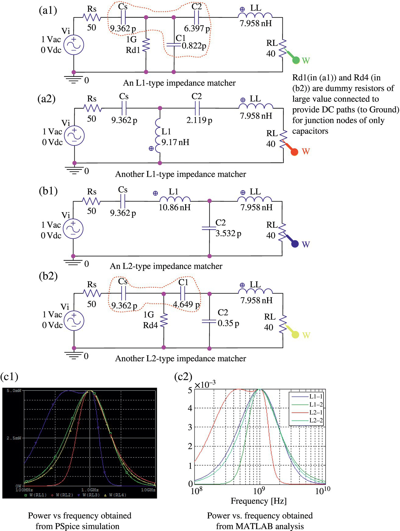
Figure 6.20 PSpice schematics for the circuits of Figure 6.19 and their plots of power PRL versus frequency.
6.3.3 T‐ and П‐Type Impedance Matchers
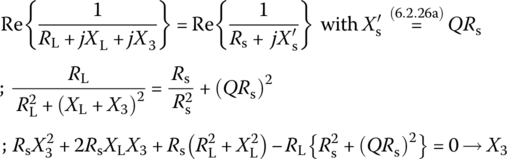
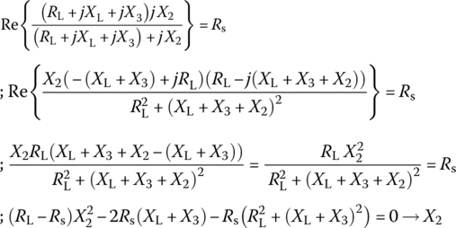
Figure 6.21 shows T‐ and П‐type LC ladders (with Zk = jXk = jωLk or Zk = jXk = 1/jωCk) that can be used to accomplish impedance matching between the source impedance Zs = Rs + jXs and load impedance ZL = RL + jXL. The conditions for impedance matching of T‐type filter (Figure 6.21(a)) with quality factor Q can be formulated into the formulas for computing Z3 = jX3, Z2 = jX2, and Z1 = jX1 as
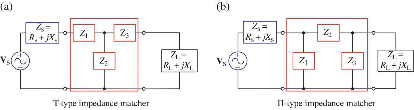
Figure 6.21 T‐ and П‐type impedance matchers.
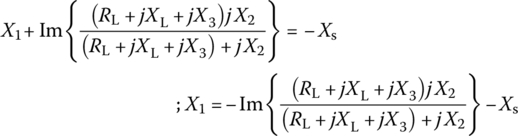
The Y‐Δ conversion of a T‐type impedance matcher yields its equivalent П‐type impedance matcher (Figure 6.21(b)).
The above MATLAB functions ‘imp_matcher_T()’/‘imp_matcher_pi()’ can be used to find possible T/П‐type LC filter(s) (with given quality factor Q) tuned for impedance matching between given source and load impedances, respectively.
6.3.4 Tapped‐C Impedance Matchers
Figure 6.24(a) shows a tapped‐C(capacitor) impedance matching circuit for a desired quality factor of Q/2 between R1 and R2. Figure 6.24(b) shows the intermediate equivalent circuit where the parallel R1|C2 part (with a target quality factor Qp to be determined) has been transformed into its series equivalent consisting of R1s‐C2s and the parallel L|R2 part (with a quality factor Q given) has been transformed into its series equivalent consisting of Ls‐R2s by applying Eq. (6.2.28a). Figure 6.24(c) shows the final equivalent circuit with the series C1‐C2s part replaced by its series combination where
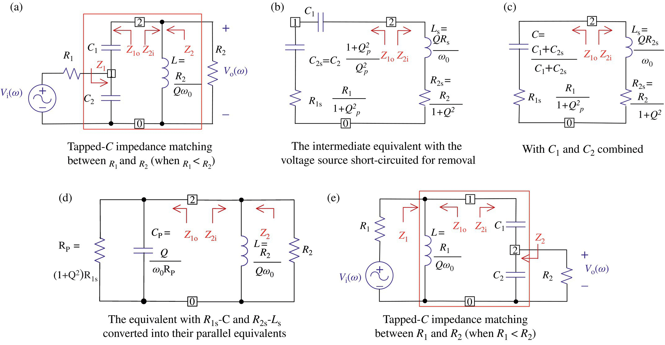
Figure 6.24 Tapped‐C impedance matching circuit and its equivalents.

Noting that if the quality factors of the source and load parts from node 2 are equally Q, their composite quality factor will be 1/(1/Q + 1/Q) = Q/2, we write the condition for the quality factor of the load (L|R2) part (i.e. the parallel combination of L and R2) to be Q as
Also, the impedance matching conditions to make the source and load impedances, Z1 and Z2, a complex conjugate pair can be written as
(6.3.8)
Once the series combination of C1‐C2s part, that is C, is determined from Eq. (6.3.8), we can use the determined value of C2s (Eq. (6.3.4c)) together with Eq. (6.3.8) to find C1:
This process of designing a tapped‐C impedance matcher has been cast into the above MATLAB function ‘imp_matcher_tapped_C()’, in which the resulting value of quality factor Q, in the variable name of ‘Qr’, is computed as

since if the series R1s‐C part (in Figure 6.24(c)) is converted to its parallel equivalent Rp|Cp while the series R2s‐Ls part (in Figure 6.24(c)) is converted back to its parallel equivalent (as shown in Figure 6.24(d)), the resistance in parallel with L and Cp is not just R2 but Rp‖R2.
6.4 Active Filter Realization
This section introduces some MATLAB functions that can be used to determine the parameters of the circuits depicted in Figures 5.17‐5.20 so that they can implement a given (designed) transfer function.
For example, we can use the MATLAB function ‘BPF_MFBa_design()’ to tune the parameters of the MFB (multiple feedback) circuit of Figure 5.20(a) so that the circuit realizes the BPF transfer function (E5.3.1) tuned in Example 5.3:
To this end, we have only to run the following statements:
>>B2=100; A2=100; A3=10000; % Desired transfer function B2*s/(s^2+A2*s+A3)>>R2=1e2; KC=3; % With R2=100 and C3=C4 given>>[C3,R1,R5,Gs]=BPF_MFBa_design(B2,A2,A3,R2,0,KC);R1= 100, R2= 100, R5= 200, C3= 1.000e-004, C4= 1.000e-004Gs = -100*s/(s^2+100*s+10000)
For another example, we can use the function ‘LPF_Sallen_design()’ to tune the parameters of the Sallen‐Key circuit of Figure 5.18(a) so that it realizes the following LPF transfer function:
More specifically, suppose we need to determine the values of R1 and R2 of the Sallen‐Key circuit of Figure 5.18(a) with the predetermined values of capacitances C1 = C2 = 100 pF so that it realizes a second‐order LPF with the DC gain K = 1.5, the corner frequency ωr = 2π × 107 [rad/s], and the quality factor Q = 0.707 (for ![]() ). To this end, we have only to run the following statements:
). To this end, we have only to run the following statements:
>>K=1.5; C1=1e-10; C2=1e-10; wr=2e7*pi; Q=0.707;% The coefficients of denominator of desired transfer ftn>>A2=wr/Q; A3=wr^2; % G(s)=K*A3/(s^2+A2*s+A3)>>KC=2; [R1,R2,Gs]=LPF_Sallen_design(A2,A3,K,C1,C2,KC);R1= 221, R2= 115, R3= 10000, R4= 5000, C1= 1.000e-010, C2= 1.000e-010Gs = 5921762640653615/(s^2+5964037174912491/67108864*s+7895683520871487/2)
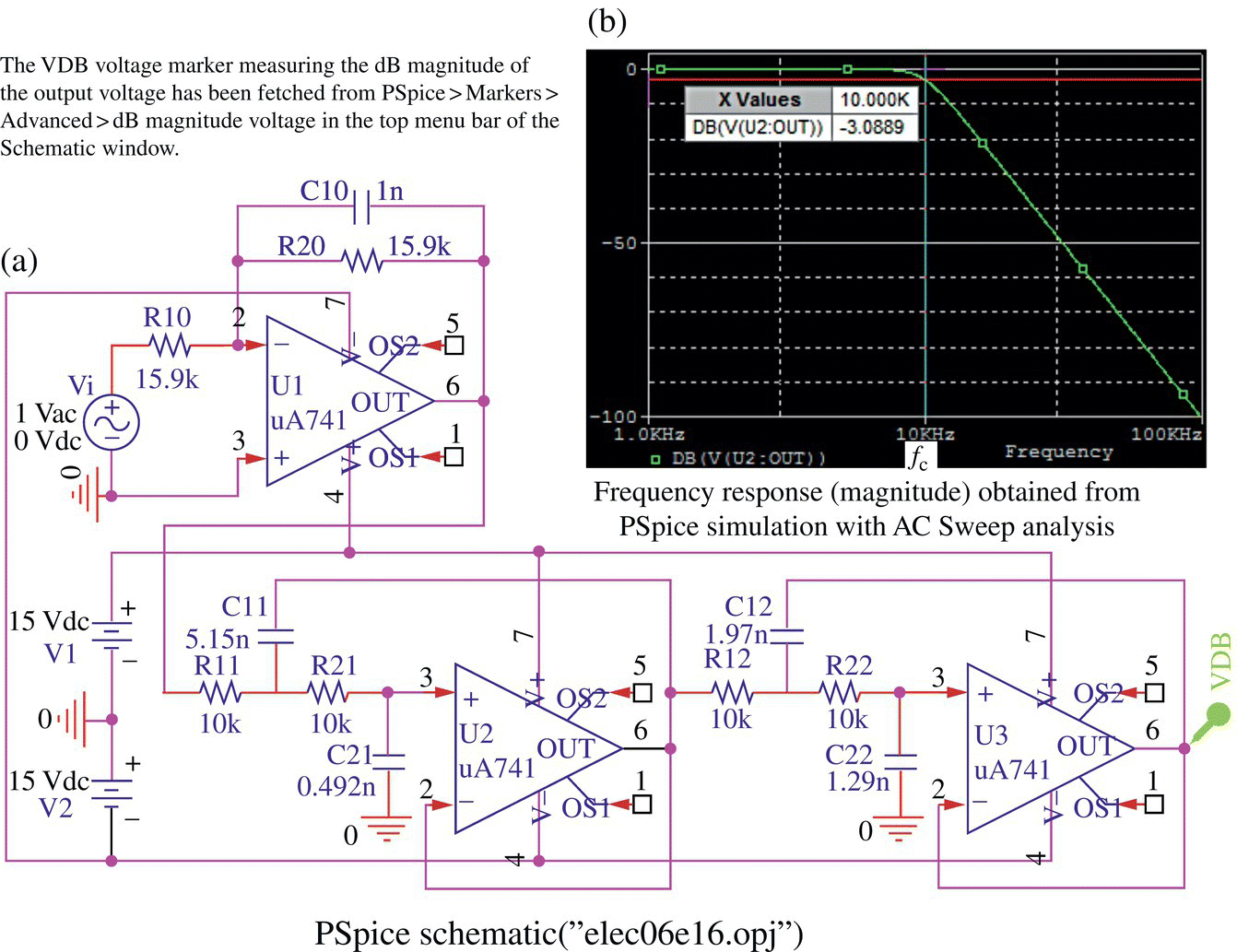
Figure 6.26 A fifth‐order Butterworth LPF implemented with one first‐order section and two Sallen‐Key LPFs.
Problems
- 6.1 Design of Passive Filter in the form of LC Ladder Circuit
- Design a Butterworth LPF with cutoff frequency fc = 2 GHz in the form of N = 5‐stage П‐type LC ladder circuit (depicted in Figure 6.14.1(a)) where the source impedance is assumed to be 50 Ω. Plot the frequency response magnitude [dB] (relative to that without the filter) to check the validity of the designed filter.
- Design a Chebyshev BPF with passband ripple Rp = 0.5 dB, peak frequency fp = 1 GHz, and bandwidth 0.1 GHz in the form of N = 3‐stage T‐type LC ladder circuit (depicted in Figure 6.14.1(b)) where the source impedance is assumed to be 50 Ω. Plot the frequency response magnitude or its reciprocal (called the insertion loss) [dB] to check the validity of the designed filter.
- 6.2 Design of Passive Filters in the form of LC Ladder Circuit
- Design a Butterworth LPF with cutoff frequency fc = 10 MHz, passband ripple Rp = 3 dB, and stopband attenuation As = 30 dB at fs = 31.62 MHz where the source and load impedances are equally 50 Ω. Note that the order of the Butterworth LPF can be determined by using the MATLAB function ‘
buttord()’ as>>wp=2*pi*7e6; ws=2*pi*31.62e6; Rp=3; As=30;[N,wc]=buttord(wp,ws,Rp,As,'s'), fc=wc/2/pi - Design a Chebyshev LPF with cutoff frequency fc = 100 MHz, passband ripple Rp = 0.01 dB, and stopband attenuation As = 5 dB at fs = 40 MHz where the source and load impedances are equally 75 Ω. Note that the minimum order of the Chebyshev LPF can be determined by using the MATLAB function ‘
cheb1ord()’ as>>wp=2*pi*1e8; ws=2*pi*4e8; Rp=0.01; As=5;[N,wc]=cheb1ord(wp,ws,Rp,As,'s') - Design a Chebyshev HPF with cutoff frequency fc = 100 MHz, passband ripple Rp = 0.01 dB, and stopband attenuation As = 5 dB at fs = 25 MHz where the source and load impedances are equally 75 Ω. Note that the minimum order of the Chebyshev HPF can be determined by using the MATLAB function ‘
cheb1ord()’ as>>wp=2*pi*1e8; ws=2*pi*25e6; Rp=0.01; As=5;[N,wc]=cheb1ord(wp,ws,Rp,As,'s') - Design a sixth‐order Chebyshev BPF with cutoff frequencies {fc1 = 10 MHz, fc2 = 40 MHz} and passband ripple Rp = 0.01 dB, where the source and load impedances are equally 75 Ω.
- Design a sixth‐order Butterworth BSF with cutoff frequencies {fc1 = 10 MHz, fc2 = 40 MHz} and passband ripple Rp = 0.1 dB, where the source and load impedances are equally 75 Ω.
- Design a Butterworth LPF with cutoff frequency fc = 10 MHz, passband ripple Rp = 3 dB, and stopband attenuation As = 30 dB at fs = 31.62 MHz where the source and load impedances are equally 50 Ω. Note that the order of the Butterworth LPF can be determined by using the MATLAB function ‘
- 6.3 Design of L‐Type Impedance Matcher for Maximum Power Transfer
Design as many L‐type impedance matchers as possible for maximum power transfer from a transmitter with output impedance Zs = 50 Ω to an antenna with input impedance ZL = RL + 1/jωCL (RL = 80 Ω, CL = 2.653 pF) at the center frequency fc = 1 GHz. Plot the power delivered to the load RL as shown in Figure 6.20 twice, once by using the MATLAB function ‘
imp_matcher_L_and_freq_resp()’ and once by using PSpice (with AC Sweep analysis type and a power marker on RL in the schematic). Which one of the L‐type filters are you going to use for impedance matching after viewing the power curves? - 6.4 Design of L‐Type Impedance Matcher
- Make as many L‐type impedance matchers as possible to match a load of ZL = 600 Ω to a source of Zs = 50 Ω at a frequency fc = 400 MHz and plot their frequency responses for some frequency band around fc.
- Make as many two‐stage impedance matchers as possible to match a load of ZL = 600 Ω to a source of Zs = 50 Ω at a frequency fc = 400 MHz where the second stage matches ZL = 600 to 173.2 Ω and the first stage matches 173.2 to Zs = 50 Ω. Use the following MATLAB function ‘
ladder_xfer_ftn()’ to find the frequency responses (for two decades around fc) and the input impedances (Zi(j2πf)'s) of the impedance matchers (with the load impedance ZL = 600 Ω) at fc. Plot the frequency responses to see if they have peaks at fc and check if Zi(j2πf)'s match the source impedance Zs = 50 Ω at fc. - Make as many L‐type filters as possible to match a load of YL = 8 − j12 [mS] to a 50 Ω line at a frequency fc = 1 GHz. Use the above MATLAB function ‘
ladder_xfer_ftn()’ to find the input impedances of the impedance matchers (with the load impedance ZL = 1/YL) and check if they match the source impedance Zs = 50 Ω at fc = 1 GHz.
- 6.5 Design of T‐Type Impedance Matcher
- Use the MATLAB function ‘
imp_matcher_T()’ to make as many T‐type filter(s) as possible matching a load of ZL = 225 Ω to a source of Zs = 15 + j15 Ω with quality factor Q = 5 at a frequency fc = 30MHz. You can visit the website https://www.eeweb.com/tools/t‐match to find two of the designs, one with DC current passed and one with DC current blocked. - Use the MATLAB function ‘
imp_matcher_T()’ to determine just the reactances constituting T‐type filter(s) to match a load of ZL = 50 Ω to a source of Zs = 10 Ω with quality factor Q = 10. (See Example 4.5 of [B-2].)
- Use the MATLAB function ‘
- 6.6 Design of П‐Type Impedance Matcher
Determine just the reactances constituting П‐type filter(s) to match a load of ZL = 1000 Ω to a source of Zs = 100 Ω with quality factor Q = 15. (See Example 4.4 of [B-2].)
- 6.7 Design of Tapped‐C Impedance Matcher
Make a tapped‐C impedance matcher to match a load of ZL = 5 Ω to a source of Zs = 50 Ω with quality factor Q = 5 at f0 = 150 MHz. Plot the frequency response magnitude curve as shown in Figure 6.25(b).
- 6.8 Design, Realization, and Implementation of High‐Order Butterworth Lowpass Filter (LPF)
Given the order, say, N = 4 and cutoff frequency, say, ωc = 2πfc =2π × 104 [rad/s] of an LPF, we can use the following MATLAB statements:
>>format short e; N=4; fc=1e4; wc=2*pi*fc;[B,A]=butter(N,wc,'s')to find the numerator (B) and denominator (A) polynomials in s of the transfer function of the desired fourth‐order Butterworth LPF as
B = 0 0 0 0 1.5585e+019A = 1.0000e+000 1.6419e+005 1.3479e+010 6.4819e+014 1.5585e+019This means the following transfer function:
(P6.8.1)
- Plot the frequency response magnitude 20log10|G(jω)| [dB] of the LPF (for the frequency range of two decades around fc = 104 [Hz]) and show that the transfer function can be realized in cascade form, i.e. as a product of second‐order transfer functions as
(P6.8.2)
or in parallel form, i.e. as a sum of second‐order transfer functions as
(P6.8.3)
In fact, this implies that the transfer function can be realized as a cascade connection of the two SOSs (second‐order sections), GC1(s) and GC2(s), or a parallel connection of the two SOSs, GP1(s) and GP2(s). You can complete and run the above MATLAB script “elec06p08a.m” to find the cascade and parallel realizations.
- Noting that each SOS of the circuit in Figure P6.8(a) has the following transfer function
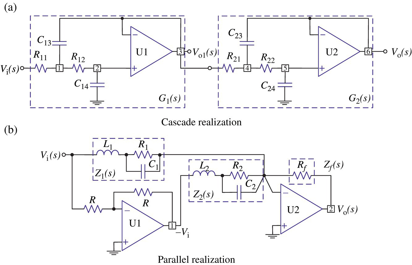
Figure P6.8 Two realizations of a fourth‐order Butterworth LPF.
(P6.8.4)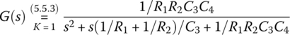
let R11 = R12 = R21 = R22 = 10 kΩ and find the values of C13, C14, C23, and C24 such that the desired transfer function will be implemented. Plot the frequency response of the cascade realization (P6.8.2) to see if it conforms with that of G(s) obtained in (a).
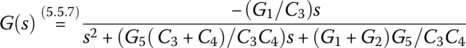
- Noting that the circuit of Figure P6.8(b) has the following transfer function
let L1 = L2 = L = 0.01 H and find the values of R1, C1, R2, C2, and Rf such that the desired transfer function will be implemented. Plot the frequency response of the parallel realization (P6.8.3) to see if it conforms with that of G(s) obtained in (a).
- Perform the PSpice simulation to see that the cutoff frequency of the two circuits, one realized in cascade form and the other in parallel form, is fc = 10 kHz at which the magnitude of the frequency response is
 = 0.7071 =
 ‐3 dB. You can use the VDB marker (from PSpice > Markers > Advanced) in the Schematic window to measure the frequency response in dB.
- Plot the frequency response magnitude 20log10|G(jω)| [dB] of the LPF (for the frequency range of two decades around fc = 104 [Hz]) and show that the transfer function can be realized in cascade form, i.e. as a product of second‐order transfer functions as
- 6.9 Frequency Scaling
Referring to Remark 6.2(2), try the frequency scaling for Example 6.17 to reduce the discrepancy between the two frequency responses, one obtained from PSpice simulation and the other obtained from MATLAB analysis. Using PSpice, plot the frequency response magnitude of the modified filter to show that you worked properly.
- 6.10 Design and Realization of High‐Order Chebyshev I Bandpass Filter (BPF)
Given the filter order, say, N = 4 and the lower/upper 3 dB frequencies, say, ωl = 2π × 8000 and ωu = 2π × 12500 [rad/s] of a BPF, we can run the following MATLAB statements to find the numerator (B) and denominator (A) polynomials in s of the transfer function of the desired fourth‐order Chebyshev I BPF.
>>format short e; N=4; Rp=3;fl=8000; fu=12500; wl=2*pi*fl; wu=2*pi*fu;[B,A]=cheby1(N/2,Rp,[wl wu],'s')This yields
B = 0 0 4.0067e+008 0 0A = 1.0000e+000 1.8234e+004 8.4616e+009 7.1985e+013 1.5585e+19meaning the following transfer function:
(P6.10.1)
This transfer function can be expressed in the form of product of two second‐order transfer functions as
(P6.10.2)
In fact, this implies that the transfer function can be realized as a cascade connection of the two SOSs, GC1(s) and GC2(s).
- Noting that each SOS of the circuit in Figure P6.10.1 has the following transfer function
(P6.10.3)
let C13 = C14 = C23 = C24 = 10 nF and find the values of R11, R12, R15, R21, R22, and R25 such that the desired transfer function will be realized. You can complete and run the above script “elec06p10.m,” which uses the MATLAB function ‘
BPF_MFBa_design()’.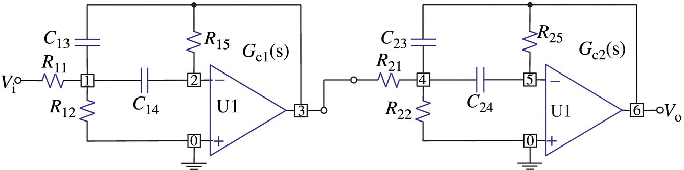
Figure P6.10.1 Cascade connection of two second‐order MFB BPFs.
- As depicted in Figure P6.10.2(a), plot the magnitude curve of the frequency response of the filter having the transfer function (P6.10.1) for f = 1–100 kHz. Does it have any ripple in the passband or the stopband? Then perform the PSpice simulation to get the frequency response of the BPF circuit that has been designed in part (a) (as depicted in Figure P6.10.2(b)). Check if the lower and upper 3 dB frequencies of the circuit are close to fl,3 dB = 8000 Hz and fu,3 dB = 12500 Hz, respectively, at which the magnitudes of the frequency response are
 = 0.7071 = −3 dB.
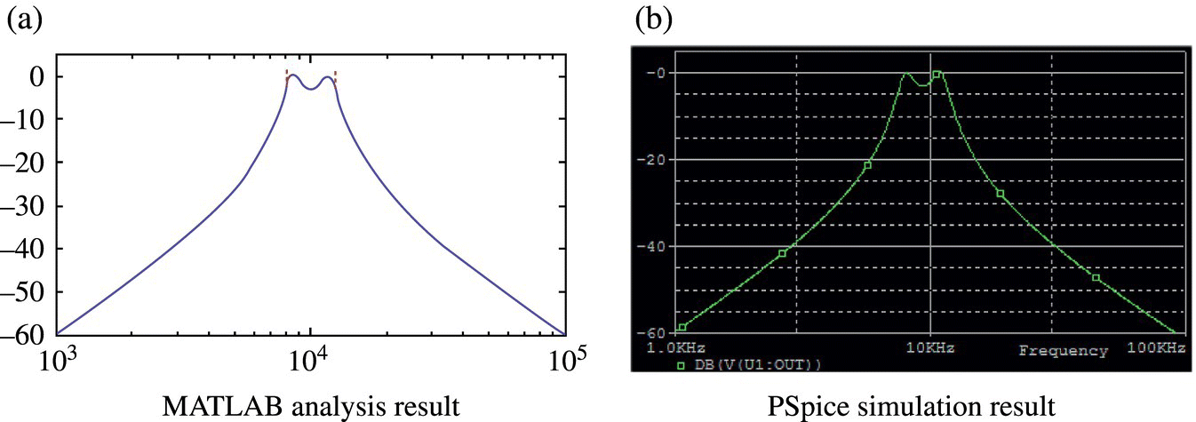
Figure P6.10.2 Frequency response of the circuit in Figure P6.10.1.
- If the PSpice simulation result tells you that the upper/lower 3 dB frequencies are considerably deviated from the expected ones, scale the capacitance values by an appropriate factor for frequency scaling (Remark 6.2(1)) and perform the PSpice simulation again to see if the upper/lower 3 dB frequencies get closer to the expected ones.
- Noting that each SOS of the circuit in Figure P6.10.1 has the following transfer function
- 6.11 Fourier Series Solution of an Active Second‐Order OP Amp Circuit Excited by a Triangular Wave
Consider the active second‐order OP Amp circuit in Figure P6.11(a), which is excited by a triangular wave voltage source of period 0.0004π as depicted in Figure P6.11(b). Find the magnitudes of the leading three frequency components (up to three significant digits) of the input vi(t) and output vo(t) in two ways, one using MATLAB and one using PSpice, and fill in Table P6.11.
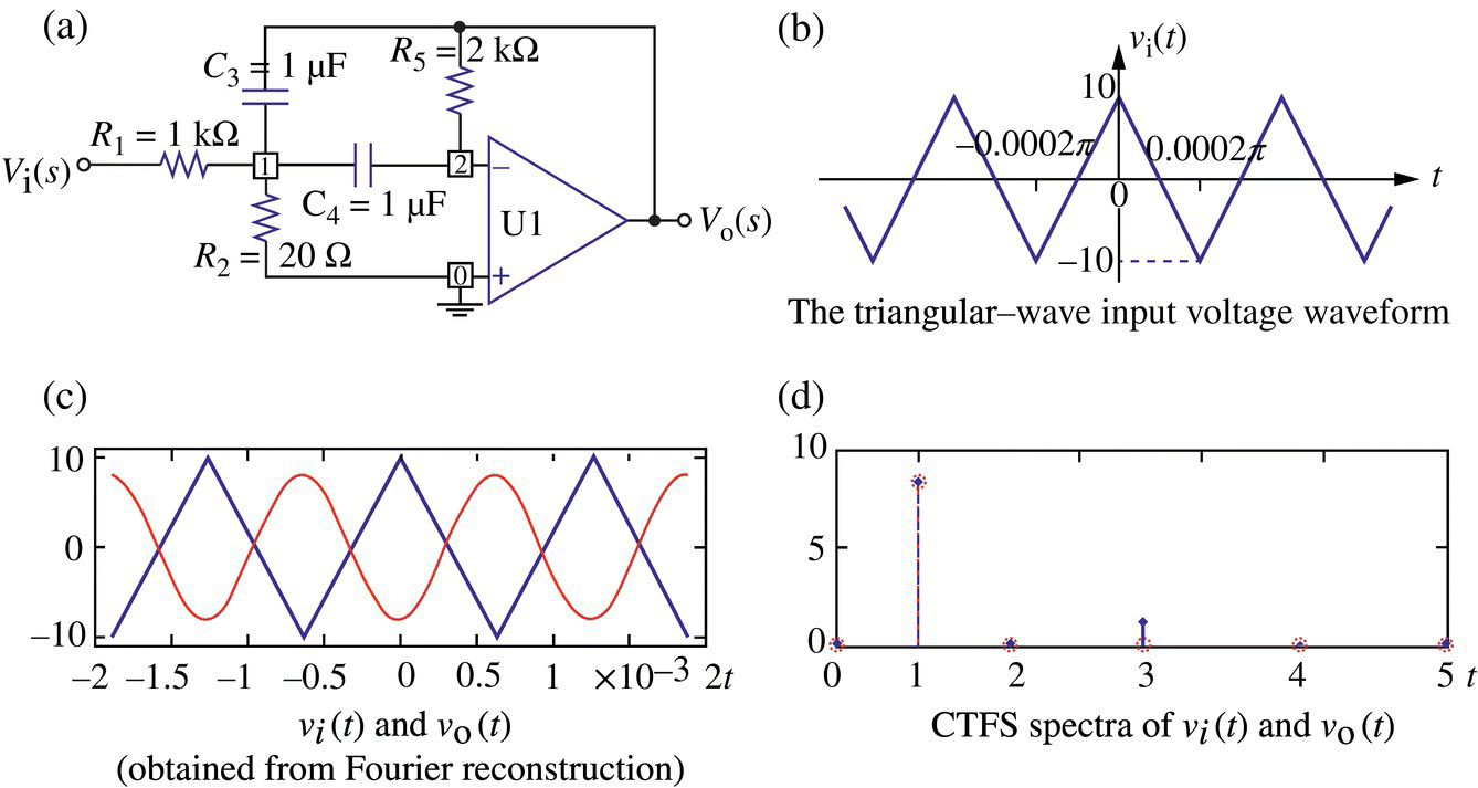
Table P6.11 Magnitudes of the leading three frequency components of vi(t) and vo(t).
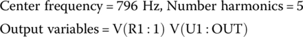
Order of harmonics k = 1 k = 3 k = 5 MATLAB PSpice MATLAB PSpice MATLAB PSpice Input vi(t) 8.11 0.903 0.324 Output vo(t) 8.16 0.0675 0.0135 - Complete the following MATLAB script “elec06p11.m,” which uses the MATLAB function ‘
Fourier_analysis()’ introduced in Section 1.5.2, together with the MATLAB function ‘elec06p11_f()’ (to be saved in a separate M‐file named “elec06p11_f.m”) and run it to get the waveforms and Fourier spectra of vi(t) and vo(t) as shown in Figure P6.11(c) and (d). - Find the peak (center) frequency ωp and bandwidth ωb of the circuit from its transfer function or frequency response. How is ωp related with the frequency component of the input passing through the filter that can be seen in the input and output spectra shown in Figure P6.11(d)?
- Use the PSpice simulation where the parameters of the periodic voltage source VPULS can be set as follows:

In the Simulation Settings dialog box, set the Analysis type, Run_to_time, and Maximum step as Time Domain (Transient), 20 ms, and 1 u, respectively, and click the Output File Options button to open the Transient Output File Options dialog box, in which the parameters are to be set as
- Complete the following MATLAB script “elec06p11.m,” which uses the MATLAB function ‘
