This chapter introduces the concept of the transmission line (TL) theory, impedance matching, and how the Smith Chart can be used for impedance matching.
7.1 Transmission Line
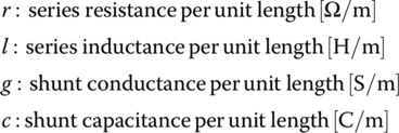
The sinusoidal steady‐state voltage and current of a TL (as depicted in Figure 7.1) at point of distance d from the load end can be written in cosine‐based phasor form as[P-1]
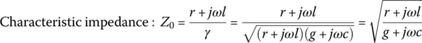
where and are called the forward(incident)/reflected voltages and currents (each propagating from the source/load to the load/source), respectively. The characteristic impedance Z0 and the propagation constant γ = α + jβ (α: attenuation constant, β: phase constant) are defined as
Figure 7.1 A transmission line (TL) terminated in a load impedance ZL.
Figure 7.2 The shapes of forward (incident) and reflected waves along the distance d from the load end.
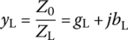
If the forward (incident) and reflected voltage phasors are
(7.1.6)
the line voltage (with angular frequency ω) at point of distance d from the load can be expressed as
(7.1.7)
Figure 7.2(a), (b), and (c) show the shapes of forward (incident) and reflected waves when the TL is open‐ended, short‐ended, and impedance‐matched, respectively.
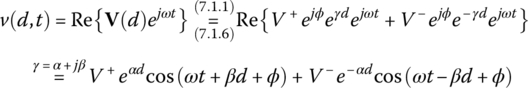
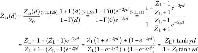
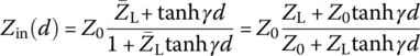
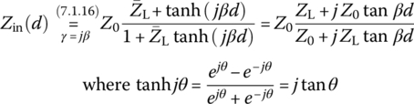
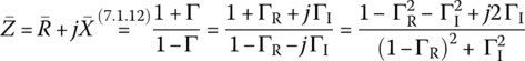
We divide V(d) (Eq. (7.1.1)) by I(d) (Eq. (7.1.2)) to get the input impedance Zin of the TL at point of distance d from the load as
(7.1.8)
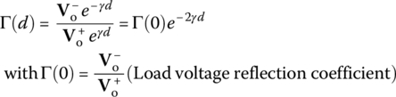
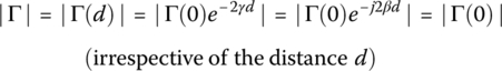
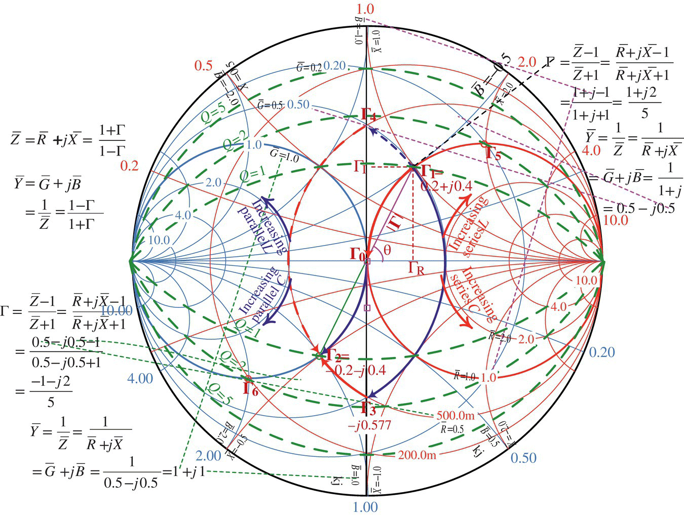
where the (input) voltage reflection coefficient Γ(d) is defined as the ratio of reflected voltage phasor to incident voltage phasor at a distance d from the load:
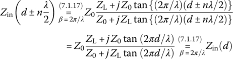
This implies that the input impedance has the same value at every one‐half wave length (λ/2), i.e. at d ± nλ/2 (n: an integer) on a lossless TL terminated with a load impedance ZL since
At points of distance d = nλ/2 (n: an integer), the input impedance of a lossless TL terminated with a load impedance ZL is the same as the load impedance:
(7.1.18)
Especially, at point of distance d = λ/4, the input impedance of a lossless TL terminated in a load impedance ZL turns out to be
(7.1.19)
This can be used to determine the characteristic impedance of a λ/4‐length lossless line, called a quarter‐wave (λ/4) (impedance) transformer, with a desired input impedance Zin,d as
(7.1.20)
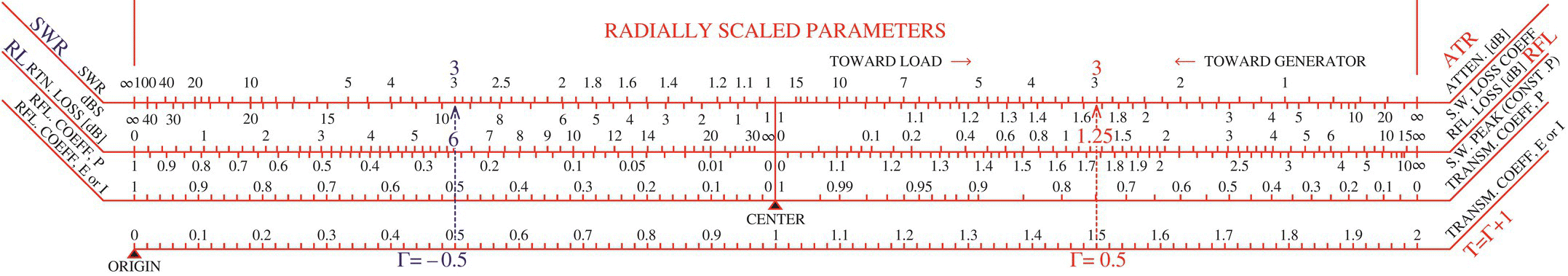
In addition to the SWR, as another measure of discontinuity at the load in a TL, the return loss (RL) is defined as the ratio of the incident power to (negatively) reflected power if Γ(0) is real‐valued and negative, i.e. Γ(0) < 0:
(7.1.21a)
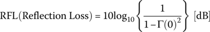
If Γ(0) is real‐valued and positive, i.e. Γ(0) > 0, the reflection loss (RFL) is defined as
(7.1.21b)
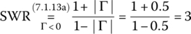
If Γ(0) = 0 (perfect impedance matching between the line and the load), we have RL = ∞ and RFL = 0. Figure 7.3 shows the lower part of Smith chart giving the SWR, RL/RFL, etc., where the values of the SWRs and RLs for Γ = −0.5 and Γ = 0.5 can be read as
(7.1.22a)
(7.1.22b)
(7.1.23a)
(7.1.23b)
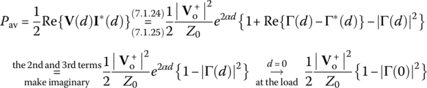
To see how the voltage reflection coefficient is related with the power flow along the TL, let us rewrite Eqs. (7.1.1) and (7.1.2) for the total voltage and current as
(7.1.24)
(7.1.25)
Figure 7.3 Lower part of Smith chart giving the Standing Wave Ratio (SWR), return/reflection loss, and reflection/transmission coefficients. (A part of the Smith chart from https://leleivre.com/rf_smith.html)
Then, the time‐average power flow along the TL at a point of distance d from the load can be written as
(7.1.26)
Here, |Γ(0)|2 may well be called the power reflection coefficient.
7.2 Smith Chart
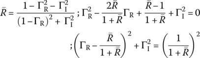
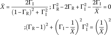
The Smith chart was developed by P. W. Smith as a graphical tool to analyze and design TL circuits, in 1939. It can be used for the conversions between reflection coefficients and normalized impedances based on Eq. (7.1.12):
Eqs. (7.2.2a,b) represent two families of circles, each called resistance circles for = constant and reactance circles for = constant, respectively, that constitute the Smith chart as plotted in Figure 7.4. Note that the center (, 0) of resistance circle gets closer to (1,0) as and the center (1,) of reactance circle moves up or down (depending on the sign of ) as .
only with the reversed sign of Γ in comparison with Eq. (7.2.1). This implies that conductance circles for = constant and susceptance circles for = constant can be obtained by making symmetric transposes of the resistance and reactance circles w.r.t. the origin (Γ = 0) or rotating them by 180° so that the sign of Γ can be reversed. In the Smith chart in Figure 7.4, conductance and susceptance circles share the point (−1,0) while the resistance and reactance circles share the point (1,0).
Note that a point on the Γ‐plane (in the Smith chart) represents the (input) voltage reflection coefficient at a distance d from the load:
Figure 7.6(b) shows several insert functions (like connecting a resistor/inductor/capacitor, an open stub, or a short(‐circuited) stub in series or parallel with the load side) that can be activated by clicking on the corresponding button in the toolbar.
7.3 Impedance Matching Using Smith Chart
7.3.1 Reactance Effect of a Lossless Line
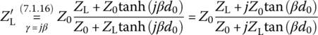
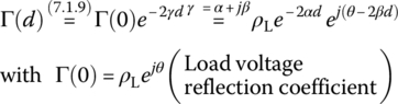
From Eq. (7.1.17), we see that connecting a lossless TL (with an imaginary propagation constant γ = jβ = j2π/λ and characteristic impedance Z0) of length l in series with a load of impedance ZL changes the impedance as
like those of an inductor or a capacitor, respectively. That is why a short‐circuited or an open‐circuited stub (line) is used for impedance matching where stubs can easily be fabricated in microstrip or stripline form compared with the ‘equivalent’ lumped element. To feel how connecting a stub line of length l in series with an impedance ZL affects the impedance in terms of its reflection coefficient Γ (on the Smith chart), let us run the following MATLAB script to get Figure 7.7. It shows that as the length of the stub increases, the reflection coefficient Γ rotates clockwise around the point Γ01 corresponding to the characteristic impedance Z01 of the stub line, which is not necessarily equal to the characteristic impedance Z0 for normalization. Figure 7.7 also shows the effect of connecting a lumped element of reactance X in series with an impedance ZL = RL + jXL is to rotate the reflection coefficient Γ clockwise/counterclockwise along the RL‐circle depending on the sign of the reactance as |X| increases where Γ = 1 for X = ±∞ (see Eq. (7.2.3) with = (R + jX)/Z0 = ±j∞ where Z0 = R0 > 0).
Figure 7.7 The effects of a stub and a lumped reactive element on the impedance.
7.3.2 Single‐Stub Impedance Matching
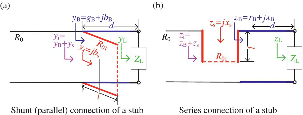
The single‐stub impedance matching (tuning) is to connect a single open‐circuited or short‐circuited lossless stub line in shunt (parallel) or series with an existing lossless TL for matching a (possibly complex‐valued) load impedance ZL to the TL of characteristic impedance R0 as shown in Figure 7.8. The problem is how distant the stub should be from the load and how long it should be.
7.3.2.1 Shunt‐Connected Single Stub
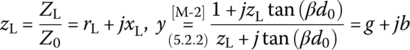
To consider how to determine the distance d from the load and the length l of the shunt stub in Figure 7.8(a), let us write the normalized impedance and admittance of the load as
where R0 and G0 = 1/R0 are the characteristic impedance and admittance of the TL, respectively, that are used to normalize the impedances and admittances. Noting that
the impedance matching is achieved when the (parallel) combination of the line‐load and the shunt stub results in a unity normalized admittance/impedance corresponding to G0/R0, i.e.
and the stub (whose admittance ys will be added to the admittance yB of the line‐load to yield the input admittance yi), short‐circuited or open‐circuited, is purely reactive/susceptive,
we should determine the distance d of the stub from the load so that the real part (conductance) of the normalized line‐load admittance can be unity:
If the stub has its own characteristic impedance R01 ≠ R0, yB should be multiplied with R01/R0. Now we determine the length l of the stub such that the susceptance can be bs = −Im{yB} to make the imaginary part of the input admittance yi = yB + ys zero, satisfying Eq. (7.3.4):
Note that OSs (open‐circuited stubs) are preferable for easy fabrication in microstrip or stripline form while SSs (short‐circuited stubs) are preferable for coax or waveguide.
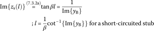
7.3.2.2 Series‐Connected Single Stub
Similarly to the case of shunt‐connected single‐stub matching, note that
the impedance matching is achieved when the (series) combination of the line‐load and the series stub (Figure 7.8(b)) results in a unity normalized impedance corresponding to R0, i.e.
and the stub (whose impedance zs will be added to the impedance zB of the line‐load to yield the input impedance zi), short‐circuited or open‐circuited, is purely reactive.
We should determine the distance d of the stub from the load so that the real part (resistance) of the normalized line‐load impedance can be unity:
If the stub has a characteristic impedance R01 ≠ R0, zB should be multiplied with R0/R01.
Now we determine the length l of the stub such that the reactance can be xs = −Im{zB} to make the imaginary part of the input impedance zi = zB + zs zero, satisfying Eq. (7.3.8):
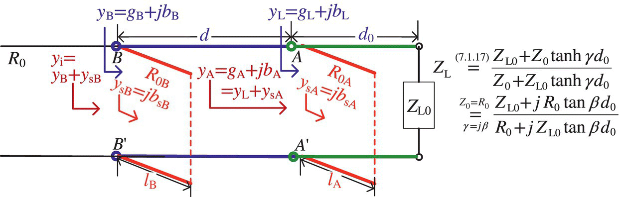
The single‐stub matching introduced in the previous section requires the stub to be attached to the main line at a specific point of precise distance from the load, presenting practical difficulties because the specified point may be undesirable to attach a stub and it is very difficult to build a variable‐length coaxial line with a constant characteristic impedance. An alternative is to attach two short‐circuited stubs at fixed positions, as shown in Figure 7.11 where the distance d0 (of stub A from a load) and distance d (of stub B from stub A) can be arbitrarily chosen and fixed (say, as λ/16, λ/8, 3λ/8, etc.), and the lengths (lA and lB) of the two stubs are determined to match the load impedance ZL0 to the characteristic impedance R0 of the main lossless line. This scheme is the so‐called double‐stub matching (tuning).
For convenience, let the serial line of length d0 be a part of the load so that the virtual load impedance can be obtained by using Eq. (7.1.17) as
(7.3.12)
Also, let us write the normalized impedance and admittance of the load as
(7.3.13a)
(7.3.13b)
where the lowercase/uppercase letters stand for normalized/unnormalized values. Then, to satisfy the impedance matching condition
(7.3.14)
the real part (conductance) of yB (the input admittance at terminals B‐B' looking into the load excluding stub B) should be 1 since ysB = jbsB (the admittance of stub B) has only an imaginary part:
and ysB = jbsB and ysA = jbsA denote the admittances of stubs B and A, respectively, that depend on their lengths as described by Eq. (7.3.2). Thus, we should first find the value of bA such that Eq. (7.3.15) can be satisfied. Then, we can determine the susceptances {bsA, bsB} of stubs A and B as
so that the susceptance value of yB can be really bsA and that of the overall input admittance can be cancelled out to be zero. Then, the stub lengths lA and lB are determined from Eq. (7.3.7). This solution process has been cast into the above MATLAB function ‘imp_match_2stub()’.
One of the drawbacks of the double‐stub matching is that it can be used for a certain range of load impedances satisfying[M-1]
Still it is not so fatal because it is easy to make this condition satisfied by using a serial line (of a certain length d0) between the load and the first stub as long as it is allowed.
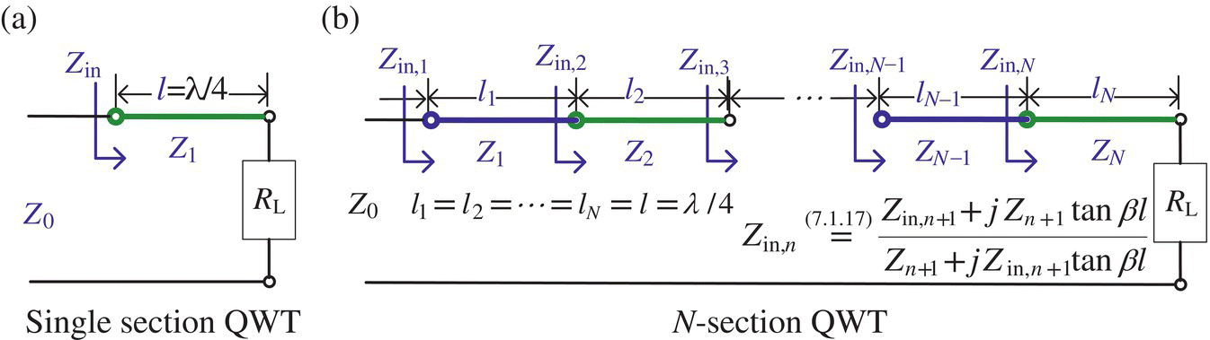
7.3.4 The Quarter‐Wave Transformer
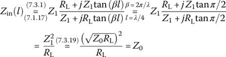
As mentioned in Section 7.1, a real load impedance RL can be matched to a feed line of characteristic impedance Z0 by using a λ/4‐length lossless line (Figure 7.13(a)), called a QWT (quarter‐wave (λ/4) (impedance) transformer), with characteristic impedance Z1
With this QWT, the reflection coefficient will be zero at β0 = 2π/λ0 (for a certain wavelength λ0) so that there is no reflected wave beyond the point distant from the load by λ0/4. However, at other frequency with βl ≠ π/2, the reflection coefficient response will be
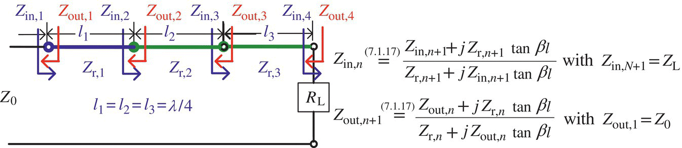
Now, we consider a multisection transformer connected between a TL of characteristic impedance Z0 and a load RL as shown in Figure 7.13 where Zn denotes the characteristic impedance of each section n. The impedance matching occurs if
(7.3.22)
where Zin,n is the input impedance of the nth section that can be obtained from Eq. (7.1.17) with the input impedance of the (n + 1)th section as the load impedance as
There are two classical N‐section transformers, the binomial transformer and the Chebyshev transformer where the reflection coefficient of the former over the frequency βd is flat while that of the latter has equiripples as a result of trying to minimize the maximum deviation for better response.
The following MATLAB function ‘multi_line()’ returns the input impedance and reflection coefficient response of a QWT with characteristic impedance vector, etc., given as input arguments.
7.3.4.1 Binomial Multisection QWT
According to the design method of binomial N‐section QWT introduced in [P-1], the characteristic impedance of each section can be approximately determined in turn from the first one as
This design process has been cast into the following MATLAB function ‘binomial_QWT()’.
7.3.4.2 Chebyshev Multisection QWT
The following MATLAB function ‘Cheby_QWT()’ uses the functions ‘chebtr2()’ and ‘chebtr3()’ implementing the Collin/Riblet algorithm (presented in [O-1]) to design Chebyshev QWTs. It regards the fourth input argument as a desired value of (minimum) fractional bandwidth or a required (minimum) attenuation [dB] in the reflectionless band (relative to unmatched case) depending on whether its value is less than 1 or not.
We can run the following MATLAB script “test_QWT.m” to use ‘binomial_QWT()’ and ‘Cheby_QWT()’ to design 1,2,3,4‐section binomial and Chebyshev QWTs and use ‘multi_line()’ to plot their reflection coefficient responses as shown in Figure 7.14, which shows the following:
Figure 7.14 Reflection coefficient responses of binomial and Chebyshev QWTs.
Chebyshev QWTs ((b1) and (b2)) have wider bandwidth than binomial QWTs ((a)).
Chebyshev QWTs with the fractional bandwidth (BW) specified have smaller ripples as the number N of sections increases.
Chebyshev QWTs with the attenuation specified have larger attenuations paying the cost of larger equiripples.
The LC ladder realization using lumped elements discussed in Section 6.3.1 has two problems if they are going to be used at microwave frequencies. First, lumped elements such as inductors and capacitors are available only for a limited range of values. Second, the distances between components is not negligible at microwave frequencies. For these reasons, distributed components like short‐ or open‐circuited stubs (TL sections) are used. To implement an LC ladder using stubs, we use Richard's transformation to convert lumped elements to stubs and then use Kuroda's identities to transform series/parallel stubs into parallel/series stubs.
<Richard's Transformation>
To understand the Richard's transformation, we need to recall Eqs. (7.3.2a,b) that the impedances of short‐ and open‐circuited stubs with characteristic impedance Z0 are
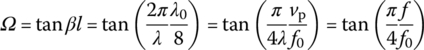
a short‐circuited stub (SS) and an open‐circuited stub (OS) of length l = λ0/8 (λ0 = vp/f0) can act as an inductor of impedance jΩL and a capacitor of impedance 1/jΩC, that is,
Here vp is the phase velocity of signal propagating on the line and f0 is some reference frequency, which is often the cutoff frequency fc of a filter implemented using the SSs and OSs, corresponding to
(7.3.29)
just like the unity cutoff frequency of a low‐pass filter (LPF) prototype. Since the tangent function is periodic in its argument with period π, the impedances of the SSs and OSs are periodic in f with period 4f0. Here, replacing inductance L and capacitance C by SS (with characteristic impedance Z0 = L) and OS (with characteristic impedance Z0 = 1/C), respectively, through Eq. (7.3.26) based on Eq. (7.3.28) (see Figure 7.15) is referred to as the Richard's transformation where their impedances are regarded as Eq. (7.3.27a,b).
Note that in principle, the inductors and capacitors of a lumped‐element filter can be replaced with SSs and OSs, respectively, and if all the stubs are of equal length, they are said to be commensurate.
<Kuroda's Identities>
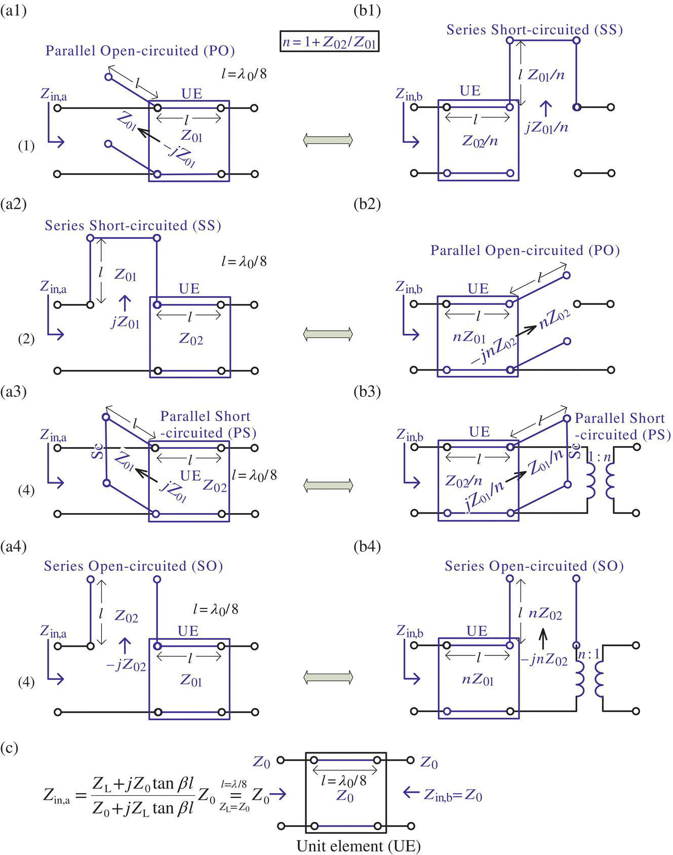
Figure 7.16(a1)‐(b4) shows the four Kuroda's identities that can be used to transform series/parallel stubs into parallel/series stubs, physically separate stubs, and change impractical characteristic impedances into more realizable ones without changing any two‐port network property such as the input and output impedances. To understand and get familiar with them, let us show the equivalence of each pair of two‐port networks in terms of the input impedance by running the following MATLAB script “show_Kuroda.m” and checking if Zin,a = Zin,b for the four identities where the ideal transformer with turns ratio of 1: n in Figure 7.16(b3) makes the load impedance ZL (on the secondary [load] side) reflected onto the primary (source) side as ZL/n2:
(7.3.30a,b)
(7.3.31a,b)
(7.3.32a,b)
(7.3.33a,b)
Figure 7.16(c) shows a unit element (UE) of characteristic impedance Z0 and length l = λ0/8 (λ0 = vp/f0) or equivalently, electrical (phase) length βl = π/4 that has input impedances at ports a and b as
(7.3.34a,b)
This implies that the frequency characteristic of a TL is not affected at frequency f0 = vp/λ0 by the (cascade) insertion of UE (a λ0/8‐long TL) if only its characteristic impedance is equal to that of the TL. That is why UEs are inserted between a TL and a distributed or lumped element as a preparation for applying some Kuroda's identity.
7.3.6 Impedance Matching with Lumped Elements
This section presents several examples illustrating how some types of impedance matchers consisting of lumped elements can be designed by using the Smith chart.
To get familiar with the Smith chart, do the following:
Compose the following MATLAB functions and save them as M‐files each named “G2Z.m” and “Z2G.m” if you don't have such similar M‐files.
function Z=G2Z(Gam,Z0) if nargin<2, Z0=1; end Z=Z0*(1+Gam)./(1‐Gam); %Eq. (7.2.1)
function Gam=Z2G(Z,Z0)if nargin<2, Z0=1; endGam=(Z‐Z0)./(Z+Z0); %Eq. (7.2.3)
For the point Γ1 = 0.2 +j0.4 (with Z0 = 50) on the Smith chart in Figure 7.4, find the corresponding impedance/admittance and their normalized values, hopefully, by using one of the above MATLAB functions. Then, plot the point Γ1 and the R‐/X‐/G‐/B‐circles passing through Γ1 by completing and running the following MATLAB script “elec07p01b.m”.
For the point Γ2 = −0.2 − j0.4 (with Z0 = 50) on the Smith chart in Figure 7.4, find the corresponding impedance/admittance and their normalized values, hopefully, by using one of the above MATLAB functions. Then, plot the point Γ2 and the R‐/X‐/G‐/B‐circles passing through Γ2 by completing and running the following MATLAB script “elec07p01c.m”.
For the points Γ1 = 0.2 +j0.4 and Γ2 = −0.2 − j0.4 (with Z0 = 50), find the corresponding impedance/ admittance and their normalized values by using the Smith Chart software ‘Smith V4.1’
Which one of the circles drawn in (b) can the Γ‐point move from Γ1 to Γ=0 along? Which one of the circles drawn in (c) can the Γ‐point move from Γ = 0 to Γ2 along?
Find the Γ‐points for Z3 = 25 +j25 (with Z0 = 50) and Y4 = 0.01 +j0.01 (with Z0 = 50).
7.2 Using the Smith Chart
In connection with Example 7.1, find two L‐type LC circuits transforming the normalized impedance Z1=1+j1[Ω] or admittance Y1=1/Z1=0.5 − j0.5 [S] represented by point Γ1 into the normalized impedance Z2 = 0.5 − j0.5 [Ω] represented by point Γ2, one via Γ4 and the other via Γ0 = 0 on the Smith chart in Figure 7.4.
7.3 Single‐Stub Shunt Impedance Matching
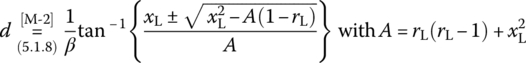
Consider the single‐stub shunt impedance matching discussed in Section 7.3.2.1 to find the distance (from the load) and length of shunt single stub so that they can match a given load impedance ZL to the lossless transmission (or feed) line of characteristic impedance Z0.
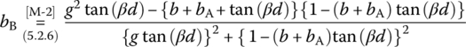
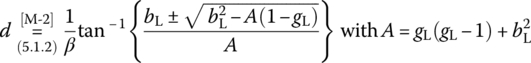
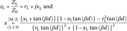
Misra [M-2] presents the following formulas for determining the distance d and length l of the shunt single stub:
(P7.3.1a)
(P7.3.1b)
where
(P7.3.2)
(P7.3.3)
Complete the above MATLAB function ‘imp_match_1stub_shunt_ Misra()’ so that it uses the above formulas to compute the distances and lengths of two shunt single stubs for impedance matching.
Use the MATLAB function ‘imp_match_1stub_shunt()’ (presented in Section 7.3.2.1) and/or the above function ‘imp_match_1 stub_shunt_Misra()’ to determine the distances (from the load) and lengths of single shunt short‐circuited stubs in the unit of wavelength so that they can match a load impedance ZL = 50 − j75[Ω] to the lossless transmission (or feed) line of characteristic impedance Z0 = 100 Ω.
Use ‘Smith 4.1’ to get the solution for the problem dealt with in (b).
7.4 Single‐Stub Series Impedance Matching
Consider the single‐stub series impedance matching discussed in Section 7.3.2.2 to find the distance (from the load) and length of series single stub so that they can match a given load impedance ZL to the lossless transmission (or feed) line of characteristic impedance Z0.
Misra [M-2] presents the following formulas for determining the distance d and length l of the series single stub:
(P7.4.1a)
(P7.4.1b)
where
(P7.4.2,3)
Complete the following MATLAB function ‘imp_match_1stub_ series_Misra()’ so that it uses the above formulas to compute the distances and lengths of two series single stubs for impedance matching.
Use the MATLAB function ‘imp_match_1stub_series()’ (presented in Section 7.3.2.2) and/or the above function ‘imp_match_1stub_series_Misra()’ to determine the distances (from the load) and lengths of single series short‐circuited stubs in the unit of wavelength so that they can match a load impedance ZL = 100 +j80 [Ω] to the lossless transmission (or feed) line of characteristic impedance Z0 = 50 Ω.
Use ‘Smith 4.1’ to get the solution for the problem dealt with in (b).
7.5 Double‐Stub Impedance Matching
Consider the double‐stub impedance matching discussed in Section 7.3.2.3 to find the lengths of stub A (at d0 from load) and stub B (at d from stub A) so that they can match a given load impedance ZL to the lossless transmission (or feed) line of characteristic impedance Z0.
Misra [M-2] presents the following formulas for determining the distance d and length l of the shunt double stub:
Complete the above MATLAB function ‘imp_match_2stub_Misra()’ so that it uses the above formulas to compute the lengths of two stubs for impedance matching.
Use the MATLAB function ‘imp_match_2stub()’ (presented in Section 7.3.2.3) and/or the above function ‘imp_match_2stub_Misra()’ to determine the lengths of two stub A (at d0 = λ/8 from load) and stub B (at d = λ/8 from stub A) in the unit of wavelength so that they can match a load impedance ZL = 100 +j50 [Ω] to the lossless transmission (or feed) line of characteristic impedance Z0 = 50 Ω.
Noting that with the distance d0 = λ/8 of stub A from the load, the virtual load impedance can be regraded as
(P7.5.4)
modify the MATLAB script “elec07e04.m” into “elec07p05.m” so that it returns the solution to this problem.
Use ‘Smith 4.1’ to get the solution for the problem dealt with in (b) where you may use some transit points (that can be found in (c)) to move the Γ‐point from ΓL to Γ0 = 0 as in Example 7.4.
7.6 Quarter‐Wave Transformer (QWT)
Consider the MATLAB function ‘chebtr()’ presented in [O-1] to design the Chebyshev QWTs (Section 7.3.4.2) satisfying the requirements for attenuation and fractional bandwidth where the attenuation is specified indirectly through reflection coefficient or SWR (standing wave ratio) as
(P7.6.1)
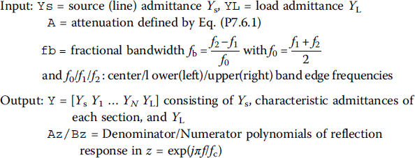
Here, |Γ1| is the reflection coefficient from the first section of the several section constituting the QWT and |ΓL| is the reflection coefficient from the load. Note that the usage of ‘chebtr()’ is as follows:
[Y,Az,Bz]=chebtr(Ys,YL,A,fb)
where
(P7.6.2)
Design a Chebyshev QWT that matches a ZL = 200 Ω‐load to a Z0=50 Ω‐line with SWRmax=1.25 over the frequency band [50, 150] MHz where the center frequency f0 = 100 MHz. You can complete and run the following script “elec07p06a.m”, which uses ‘chebtr()’ to design such a QWT. Noting that the characteristic admittance vector Y returned as the first output argument of ‘chebtr()’ contains Ys/YL, as the first/last entry, tell the number of sections and characteristic impedances of each section of the designed QWT.
To see if the above design Zr satisfies the following QWT conditions:
Noting that the fifth input argument of ‘multi_line()’ (presented in Section 7.3.4) should have the normalized phase constant β = 2π as the first entry, use the MATLAB function to get the reflection response of the QWT designed in (a) and plot it together with SWR (Eq. (7.1.13a)) for the frequency range 0~2fc. To this end, complete and run the following script “elec07p06c.m” to get the graphs as shown in Figure P7.6.2.
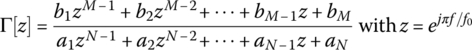
To realize the meanings of the second/third output arguments of ‘chebtr()’ as the denominator/numerator polynomials of the reflection response in z = exp(jπf/f0), use them to compute the reflection response
(P7.6.5)
and see if it conforms with that obtained as the second output argument of ‘multi_line()’ in (c) by running the following MATLAB script “elec07p06d.m”.
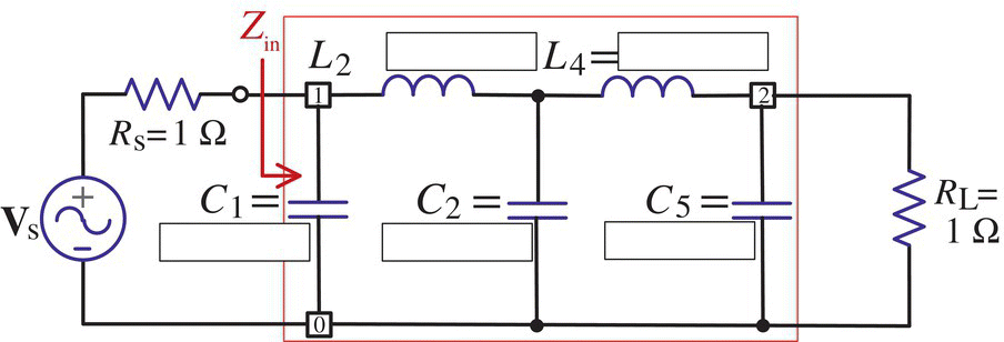
With source/load impedances Rs = 50 [Ω]/ZL = 50 [Ω], design a Chebyshev I LPF with passband ripple Rp = 0.5 dB for f ≤ fp (passband edge frequency) = 3 GHz and stopband attenuation As = 40 dB for f ≥ fs (stopband edge frequency) = 6 GHz for fabrication using microstrip lines with shunt stubs only.
Referring to Example 7.5, take the following steps to design such an LPF:
(Step 0) Determine the order N and cutoff frequency ωc [rad/s] of the LPF to satisfy the given frequency response specifications by running the following MATLAB statements:
With the results, fill in the parameter values in Figure P7.7.2(a).
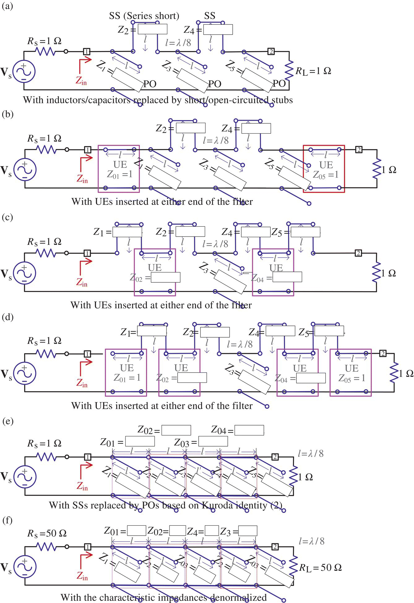
(Step 4) Noting that even if we are going to convert every stub into parallel (shunt) stubs, we provisionally should convert the two Po's (parallel open‐circuited stubs) Z1 and Z5 (at either ends) into Ss's (series short‐circuited stubs) so that the Ss's Z2 and Z4 can have UEs of Z0 = 1 (needed for conversion), let us use Kuroda identity 1 to convert Z1 and Z5 into Ss's. Thus, we insert UEs between Z1/Z5 and the transmission line (as Figure P7.7.2(b)) and run the following statements:
Figure P7.7.1 Normalized prototype LPF of order N = 3.
With the results, fill in the parameter values in Figure P7.7.2(c).
(Step 5) Noting that in Figure P7.7.2(c) the two Ss's Z1 and Z5 (at either ends) have no UE needed for conversion (while Z2 and Z4 have UEs), let us insert UEs of Z0=1 between them and TL as shown in Figure P7.7.2(d).
>>Z0s(1)=1; Z0s(5)=1;
(Step 6) Now that every Ss has got its UEs for conversion, let us use Kuroda identity 2 to convert the Ss's Z1, Z2, Z4, and Z5 into Po's by running
 >>for m=[1 2 4 5]
       [Z0s(m),Zs(m),SPsos{m}]=Kuroda(Zs(m),SPsos{m},Z0s(m));
   end
   Z0s, Zs, SPsos
With the results, fill in the parameter values in Figure P7.7.2(e).
Alternatively, the process from Step 4 to Step 6 can be performed by using the MATLAB function ‘S2P_stubs()’ (listed below) as follows:
(Step 7) Denormalize the normalized characteristic impedances by multiplying them with Rs = 50 Ω:
>>Zs=Zs*Rs, Z0s=Z0s*Rs
With the results, fill in the parameter values in Figure P7.7.2(f).
(Step 8) Frequency scale the circuit by determining the line/stub lengths as l = λ/8 = vp/fc/8 [m] where vp [m/s] is the phase velocity of signal propagating on the line and fc is the cutoff frequency given as a design specification.
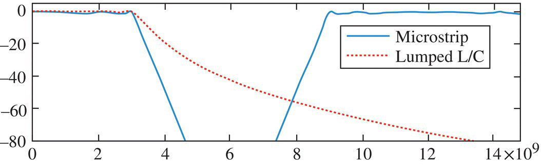
(Step 9) To plot the frequency responses of the two filters, one (called a lumped‐element filter) consisting of lumped elements L/C (Figure P7.7.1) and the other (called a distributed‐element filter) consisting of microstrip lines/stubs (Figure P7.7.2(f)), complete and run the following MATLAB script “elec07p07b.m” to get the frequency responses as shown in Figure P7.7.3:
Figure P7.7.3 Frequency responses of the lumped‐element filter and distributed‐element filter.
Note that the whole process from Step 1 to Step 7 can be performed by using the MATLAB function ‘ustrip_LPF()’ (listed below) as follows:
7.8 Design of T‐type Impedance Transformers Using the Smith Chart
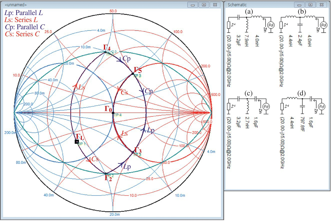
Consider making T‐type ladders with quality factor Q = 2 for transforming ZL = 20 − j15[Ω] to Zs = 50[Ω] at frequency fc = 2 GHz.
Complete and run the following MATLAB script “elec07p08.m” to make such T‐type ladders.
Referring to Figure P7.8, note that, with Q ≤ 2, there are four paths along resistance/conductance curves from point ΓL (representing ZL = 20 − j15 [Ω]) to Γs (representing Zs = 50 [Ω]), each via Γ2‐Γ3, Γ4‐Γ3, Γ2‐Γ5, and Γ4‐Γ5 where Γ2 and Γ4 are on the lower and upper Q = 2‐circles, respectively. Use ‘Smith V4.1’ to solve the same design problem as (b).
7.9 Impedance/Admittance from Resistance/Conductance
Complete the following MATLAB function ‘RG2ZY()’ so that it can return the impedance Z and admittance Y with given resistance R and conductance G. Use it for R5 = 60 Ω and G5 = 0.01 S (Eq. (E7.8.2)) to check if it works properly.


 (P7.3.1b)
 (P7.3.3)
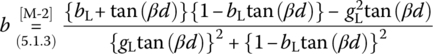
 (P7.4.1b)
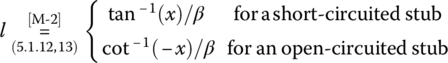
 (P7.5.3b)