
Appendix H
OrCAD/PSpice®
OrCAD PSpice®, formerly MicroSim PSpice® (Professional Simulation Program with Integrated Circuit Emphasis), is a powerful circuit simulation program with graphic interface to analyze electric and electronic circuits. You can download the OrCAD demo software together with the OrCAD flow tutorial at the web site http://www.cadence.com/products.
H.1 Starting Capture Component Information System (CIS) Session
Once you have installed the OrCAD software, you may start the Capture Component Information System (CIS) Demo session by clicking the corresponding icon to open the Capture CIS Window (Figure H.1), in which you can click File> New> Project on the menu bar to open the New Project dialog box (Figure H.1(b)). Here, you are supposed to do the following in the New Project dialog box:
- In the Name field, type, say, ‘test’ (with no quotation mark) as a new project name.
- Check the radio button of Analog or Mixed A/D.
- In the L ocation field, type the pathname of the subdirectory in which you want the new project to be saved. You can use the Browse button to select the location for the project files and click OK.
- Then click OK to close the New Project dialog box, which will make the Create PSpice Project dialog box pop‐up.
- Check the radio button of Create a blank project and click OK in the Create PSpice Project box (Figure H.1(c)).
Then you will see the activated Capture (CIS) Window with the menu bar together with the tool bar, which has the Project Manager Window containing the design file name ‘test.dsn’ under the subdirectory named ‘Design Resources’ on the left side (Figure H.2). You can click the design file name (like ‘test.dsn’) and successively, SCHEMATIC1 and PAGE1 to open the Schematic Editor Window, in which you can draw the schematic for the circuit which you would like to analyze.
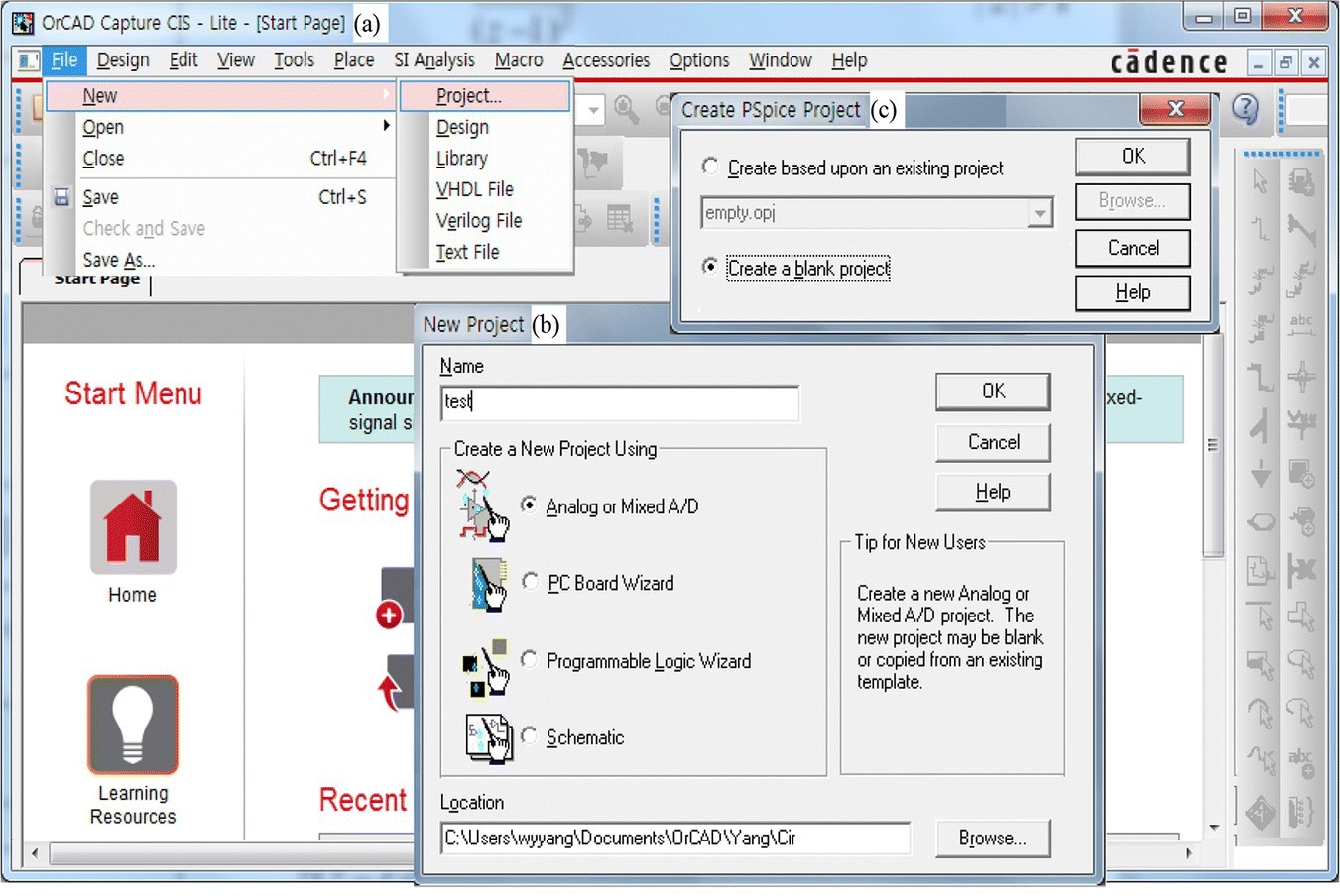
Figure H.1 New Project dialog box opened by clicking File>New>Project in the Capture Component Information System (CIS) Window.
H.2 Drawing Schematic
H.2.1 Fetching Parts (Place>Part or ‘p’)
Click Place/ Part on the menu bar or the Place Part button on the tool palette, or just press the ‘p’ key on the keyboard to open the Place Part dialog box (Figure H.2), in which you can either scroll through the part list and select (click) the needed part or just type the part name into the Part field in the upper part of the dialog box. It may be helpful for you to know the part names representing some often‐used device types listed in Table H.1. In case you cannot find the device (component) you want to place from the current part list, you need to search for it after clicking the Part Search button and then add the library (like oolscapturelibrarypspice‘analog.olb’, ‘source.olb’, ‘eval.olb’, ‘breakout.olb’, ‘special.olb’, ‘sourcstm.olb’ etc.) containing the device.
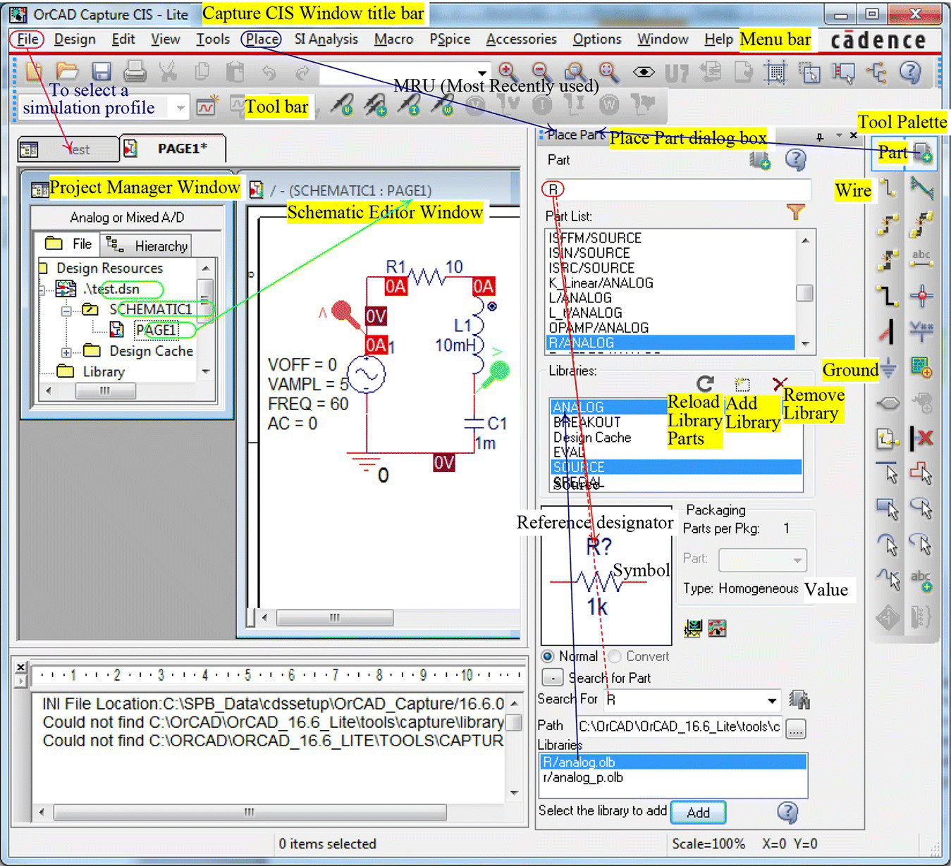
Figure H.2 Capture window, Project Manager window, Schematic Editor Window, and Place Part dialog box opened by clicking the Place Part button in the Tool Palette.
Table H.1 Device types and PSpice part names.
| Device type | Part name | Device type | Part name |
| Capacitor | C | Inductor | L |
| Diode | D | Bipolar junction transistor (BJT) | Q |
| Voltage‐controlled voltage source (VCVS) | E | Resistor | R |
| Current‐controlled current source (CCCS) | F | Switch to be closed at specified time | Sw_tClose |
| Voltage‐controlled current source (VCCS) | G | Switch to be opened at specified time | Sw_tOpen |
| Current‐controlled voltage source (CCVS) | H | OP Amp | uA741 |
| Independent current source | I | Independent voltage source | V |
| Independent AC current source | IAC | Independent AC voltage source | VAC |
| Independent DC current source | IDC | Independent DC voltage source | VDC |
| Independent periodic current source | IPULSE | Independent periodic voltage source | VPULSE |
| Independent piecewise linear current source | IPWL | Independent piecewise linear voltage source | VPWL |
| Sinusoidal current source | ISIN | Sinusoidal voltage source | VSIN |
| Transformer | XFRM_LINEAR |
H.2.2 Placing Parts
Once you have got the wanted part as can be inspected from the graphic symbol displayed in the preview box at the bottom‐right corner of the Place Part dialog box, click OK to close the dialog box. Then the selected part attaches to the mouse pointer so that we can move and place it anywhere on the schematic page by clicking. The device will remain attached to the mouse pointer, so you may use it as many times as needed. To detach the device from the mouse pointer, press ESC key or right‐click and click (select) End Mode in the pop‐up menu. You can have one of the recently fetched devices attached to the mouse pointer by clicking (selecting) it among the MRU list in the center part of the tool bar just below the top menu bar. You can select any part on the schematic by clicking it so that it gets pink‐hot and then rotate it counterclockwise by pressing the ‘r’ key or mirror it horizontally/vertically by pressing the ‘h’/‘v’ key. You can also select any area of the schematic by clicking one corner of the area and dragging (pressing/holding the left mouse button) to the opposite corner and then move(click and drag), cut(‘^x’), paste(‘^v’), delete(Del), rotate(‘r’), or mirror horizontally(‘h’)/vertically(‘v’) the selected (pink‐hot) area, where ^ indicates ‘with the CTRL key held down’ You can zoom in/out the whole schematic by pressing the ‘i’/‘o’ key. After placing all the parts at the appropriate locations, you should click the GND (ground) button on the tool palette, click (select) 0/SOURCE in the Place Ground dialog box, click OK to close the dialog box, and move the mouse pointer (with the Ground symbol attached to it) to click at an appropriate location to place the ground symbol at that location.
H.2.3 Defining(Assigning)/Changing Part Values
You can double‐click the value or reference designator of a part to define/change it in the Display Properties dialog box, or double‐click the part to open its Property Editor spreadsheet, define or change the values of the parameters, and even create a new parameter (New Column) and set its value. Figure H.3 shows the waveforms of sine/pulse/piecewise‐linear/digital sources and their Property Editor spreadsheets, in which the parameters are defined and changed. Sometimes, you should set the value of initial condition (IC) for inductors/capacitors, where IC denotes the initial current/voltage for inductor/capacitor, respectively. Table H.2 shows magnitude identifiers used by PSpice.
H.2.4 Wiring (Place>Wire or ‘w’)
In order to connect the parts here and there in the Schematic page, you click the menu Place/ Wire on the menu bar or the Place Wire button on the tool palette, or just press the ‘w’ key on the keyboard to change the arrow‐type pointer into a cross‐type pointer, which you can use like a pencil. Then click the one point of the connection you want to make, click successively the intermediate points, and either double‐click the other point or right‐click the other point and click (select) End Wire in the pop‐up box. You can draw a slant line by holding down the SHIFT key and clicking the connection points. To stop wiring, press ESC key or right‐click and click (select) End Wire in the pop‐up box.
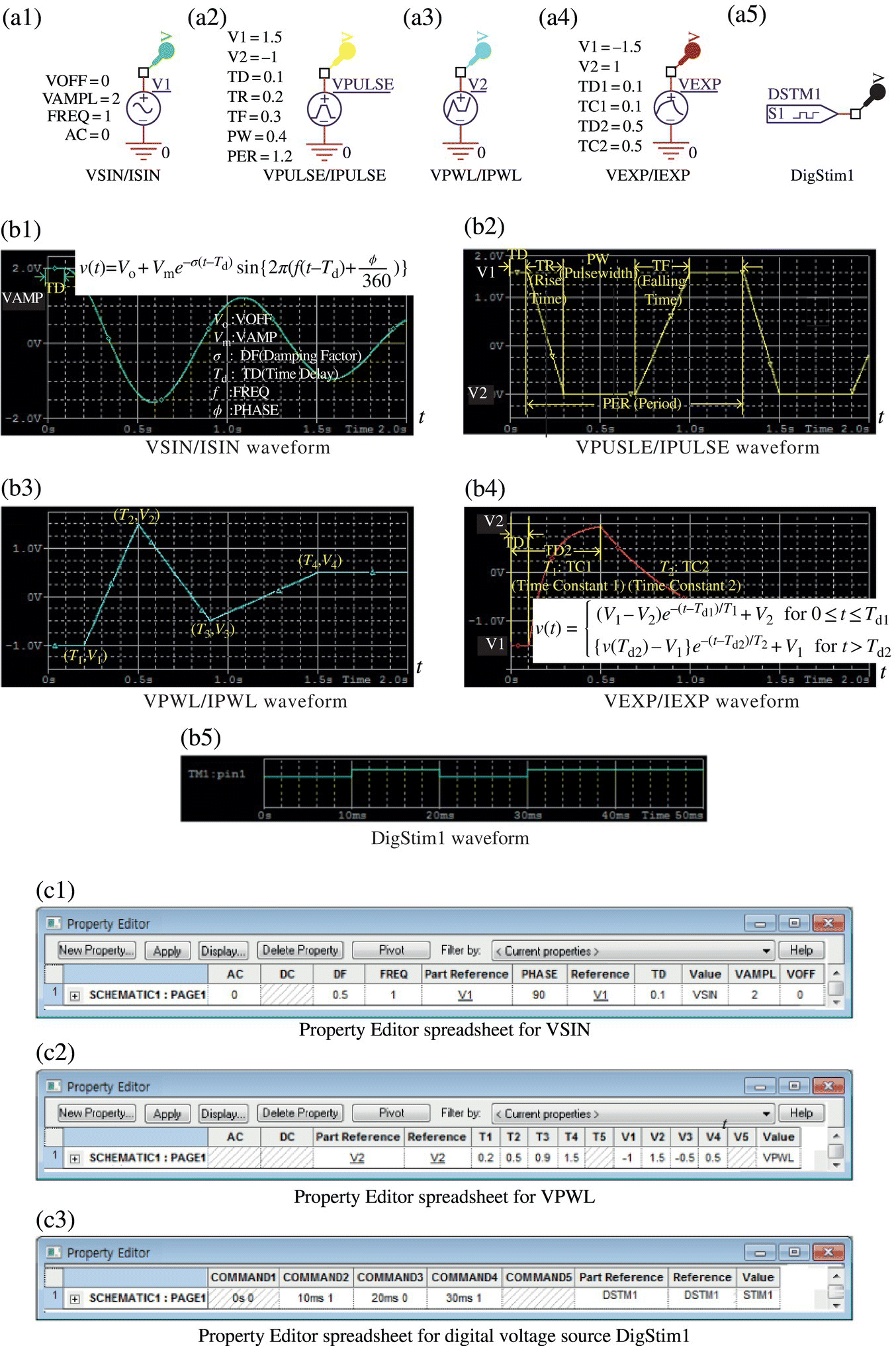
Figure H.3 Waveforms and Property Editor spreadsheets of the sources VSIN/VPULSE/VPWL/VEXP/STIM1.
Table H.2 Magnitude identifiers used by PSpice (Capture).
| Unit identifier | F or f (femto) | P or p (pico) | N or n (nano) | U or u (micro) | M or m (milli) | K or k (kilo) | MEG or meg (mega) | G or g (giga) | T or t (tera) |
| Magnitude | 10−15 | 10−12 | 10−9 | 10−6 | 10−3 | 103 | 106 | 109 | 1012 |
(cf.) PSpice does not require the units in specifying the part values; but if the unit is shown, there must be no space between the value and the unit. In fact, PSpice does not differentiate the uppercase and lowercase letters.
H.3 Setting Simulation Conditions
H.3.1 Creating Simulation Profile
To set the simulation conditions, click P Spice/New Simulation Profile on the menu bar or the corresponding button on the tool bar to open the New Simulation dialog box, in which you can type a profile name, say, ‘tran’ (with no quotation mark) into the Name field and click the Create button (Figure H.5(a)). Then the Simulation Settings dialog box is opened, in which you can do the following:
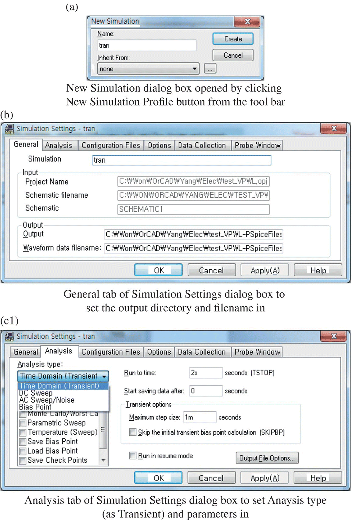
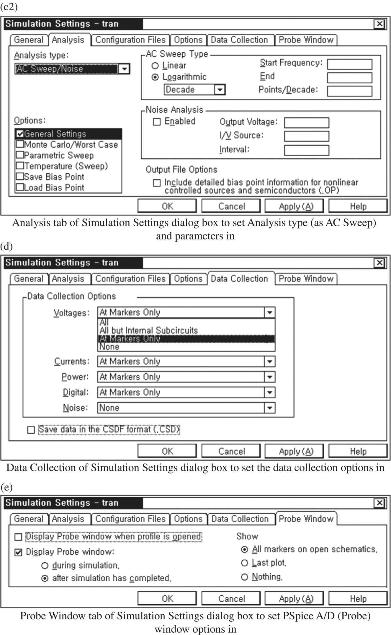
Figure H.5 Setting the simulation conditions in the Simulation Settings dialog box.
- Click on the General tab to set the output directory and waveform data filename (Figure H.5(b))
- Click the Analysis tab to set the Analysis type to one of {Time Domain (Transient), DC Sweep, AC Sweep, and Bias Point}, select the Options, and set the simulation time/frequency range, etc. (Figure H.5(c1) or (c2)). Especially in the case of transient analysis, you can click the Output File Options button to make the results of Fourier analysis and/or operating bias point analysis printed into the output file.
- Click the Data Collection tab to select Data Collection Options (Figure H.5(d)).
- Click the Probe Window tab to set the conditions on PSpice A/D (Probe) window (Figure H.5(e)).
- Most often, you are supposed to do only the second thing about the Analysis type and the related parameters.
H.3.2 Placing Voltage/Current Markers (Probes) – PSpice>Markers
To obtain the voltage/current/power waveform, you can click P Spice> Markers on the menu bar and select one of {Voltage Level, Voltage Differential, Current, Power Dissipation, Advanced (dB, Phase, Real, Imaginary)} from the submenu or click one of {V, Vd, I, W}‐Marker buttons on the tool bar to have the probe pins attached to the mouse and then put one at each target point/device on the schematic. The probe pin will remain attached to the mouse pointer, so you may use it as many times as needed. To detach the probe pin from the mouse pointer, press ESC key or right‐click and click (select) End Mode in the pop‐up menu. Alternatively, you can use the Add Trace function in the Probe window in order to make measurements of any voltage/current/power without using schematic markers. Specifically, you can click Trace> Add_Trace on the menu bar or the Add Trace button on the tool bar of the Probe window to open the Add Traces dialog box, select the variables from the Simulation Output Variables list, and click OK. On the other hand, you can have all the values of voltage/currents (at the operating point) displayed/hidden on the schematic by clicking the Enable Bias Voltage(V)/Current(I)/Power(W) Display button on the tool bar of the Schematic Editor Window.
H.3.3 Editing Simulation Profile
To modify the simulation conditions, either click P Spice> Edit Simulation Profile on the menu bar or the corresponding button on the tool bar in the Capture window, or click Simulation/ Edit Profile on the menu bar or the corresponding button on the (left) tool bar in the Probe window to reopen the Simulation Settings dialog box, in which you can change the simulation conditions and the related parameters. In case there is any existing Simulation Profile, you can select it from the Simulation Profile list on the left side of the tool bar in the Capture window.
H.4 Running PSpice Simulation and Observing the Results
To perform the simulation of the circuit you have drawn in the schematic page, either click PSpice> Run on the menu bar or the corresponding button (of right arrow shape) on the tool bar in the Capture window, or click Simulation/Run on the menu bar or the corresponding button on the right side of the tool bar in the Probe window. Pressing the ‘F11’ key is another way to perform the simulation. Then you will see the waveforms of the voltages/currents/powers which you have chosen as the measurement outputs by placing the corresponding Markers. Besides, you can find their peaks, troughs, minimum, maximum, etc. as if you had a digital storage oscilloscope.
H.4.1 Analyzing Waveforms – Trace>Cursor
Suppose we have drawn the schematic of an RLC circuit as Figure H.6(a) and performed the simulation to get the result as Figure H.6(b) in the PSpice A/D (Probe) window. Then you can click Trace/ Cursor on the menu bar or the Toggle Cursor button on the tool bar in the Probe window to have two cross‐type cursors appear on a waveform, each of which can be moved either by left‐/right‐clicking at any desired position or by pressing the left or right Arrow/Shift+Arrow key, where the coordinates of the cursor points on the waveform together with their pairwise differences can be seen in the Probe Cursor box. In case you have several waveforms in the Probe window, you can select the waveform to be traced using each cursor by left‐/right‐clicking on the graphic symbol next to the name of the variable (in the legend just below the waveform graph) which you want to trace. Once you have moved a cursor, you can find the peak|trough|minimum|maximum|… of the waveform associated with that cursor by clicking Peak|Trough|Min|Max|… on the menu bar or the corresponding button on the toolbar. You can also click Trace> Evaluate_Measurement on the menu bar or the Evaluate Measurement button on the toolbar to open the Evaluate Measurement dialog box and select a desired measurement (such as the maximum, the minimum, the center frequency, the bandwidth, etc.) and a simulation output variable so that the target trace expression will appear in the Trace Expression field at the bottom of the Evaluate Measurement dialog box as illustrated in Figure H.7. (You may directly type the target trace expression into the Trace Expression field.) Then you can click OK to have the desired measurement results appear at the bottom of the Probe window as illustrated in Figure H.6(b).
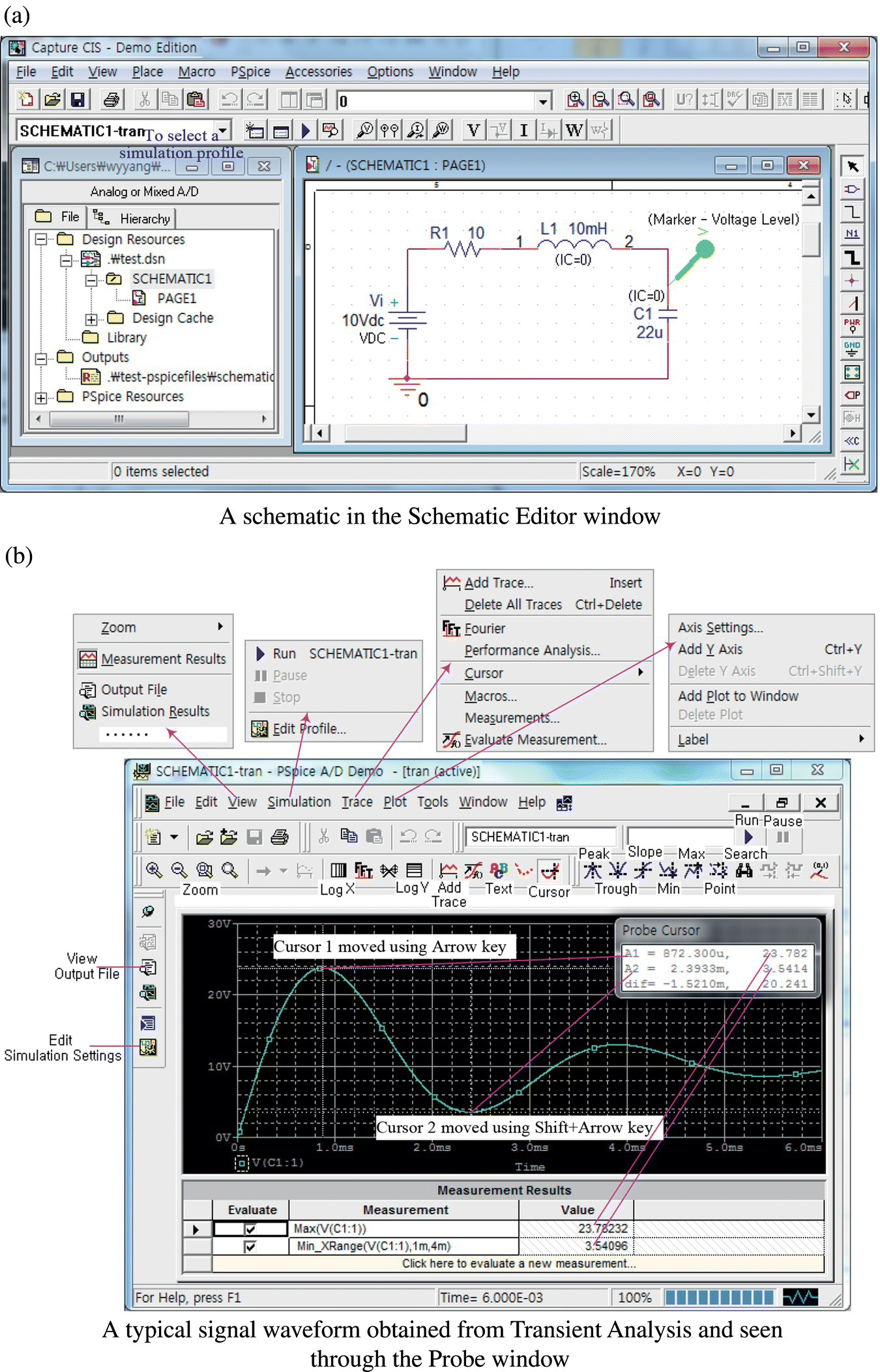
Figure H.6 A typical schematic and its simulation result.
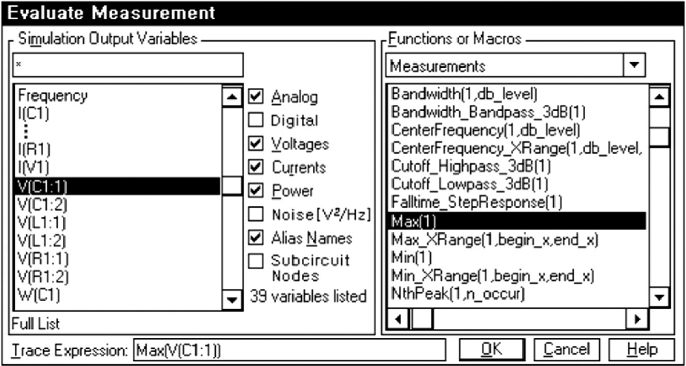
Figure H.7 Evaluate Measurement dialog box.
H.4.2 Adding/Removing Waveforms – Trace>Add_Trace or ‘Ins’/Del key
To see the waveform of another variable (Figure H.8(b)), you can click the Voltage/Current/Power Marker button on the toolbar of the Schematic Editor Window and put the probe pin at the target node or element. Alternatively, you can just press the ‘Ins’ key or click Trace> Add_Trace on the menu bar or the Add Trace button on the toolbar (of the Probe window) to open the Add Traces dialog box (Figure H.8(a)) and enter the target trace expression into the Trace Expression field (at the bottom) directly or by selecting related variable(s) from the Simulation Output Variable list (on the left side) and/or operator/function from the Function or Macro list (on the right side). You can delete any existing waveform by clicking the variable name below the waveform graph and pressing the ‘Del’ key.
In case the plotted variables differ in the order of magnitude and/or the unit so that you feel like having another graph on which to plot one or some of them, you can click Plot>Add_ Plot_to_ Window on the menu bar (of the Probe window) to add another graph as illustrated in Figure H.8(c), press the ‘Ins’ key to open the Add Traces dialog box, and then enter the trace expression to plot in the new graph. Note that you might have to increase the vertical size of the Probe window to make it accommodate additional graph(s) to be created. After getting more than one graph, you can select one of them by clicking it so that you can modify it, where the selected graph is denoted by ‘SEL>>’ If you want to delete a graph, click the graph for selection and then click Plot>De lete_Plot on the menu bar (of the Probe window) for deletion.
If you have got any data file on the same‐named variable for the same range in another simulation, you can plot it in the same graph by clicking File>Append_ Waveform(.DAT) on the menu bar or the Append File button and then selecting the data file.
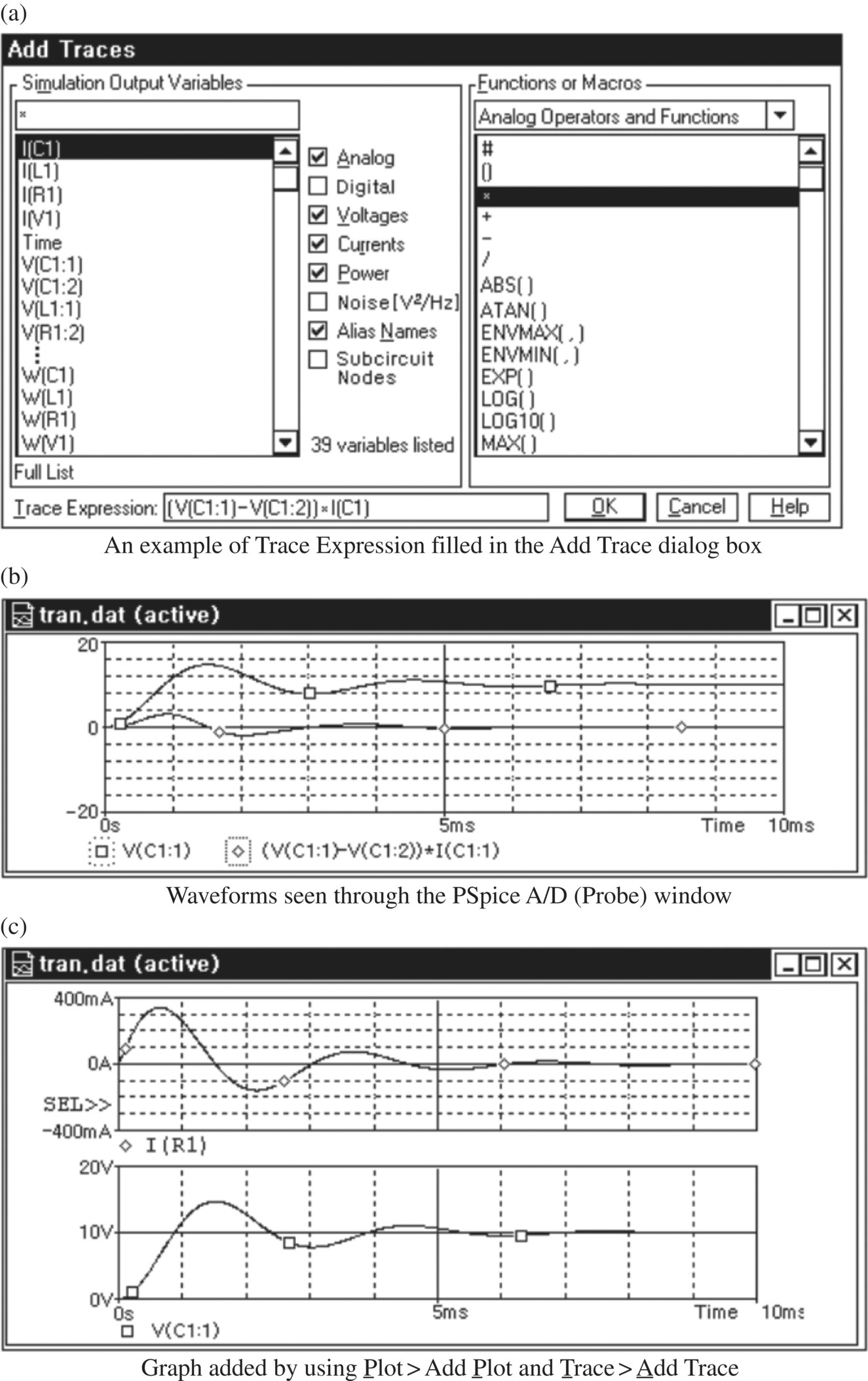
Figure H.8 Adding waveform(s) (using Add Trace and Add Plot).
H.4.3 Processing Waveforms/Graph
You can scale up/down the graph by either pressing the ‘^i’|‘^o’ key or clicking View> Zoom> ( In| Out) on the menu bar or the Zoom_(In|Out) button on the toolbar, and then clicking at any point around which the graph will be zoomed in|out by a factor of 2. You can scale up/down a partial area of the graph by either pressing the ‘^a’ key or clicking View> Zoom> Area on the menu bar or the Zoom_Area button on the toolbar, and then dragging the mouse pointer from a corner point to the opposite one to get the area selected. You can click View> Zoom> Fit on the menu bar or the Zoom_Fit button on the toolbar to have the whole waveform(s) fit the graph.
You can also click the Plot>Axis_ Settings menu or double‐click the x‐ or y‐axis to open the Axis Settings dialog box (Figure H.9) and select a tab of { X‐Axis, Y‐Axis,X‐ Grid,Y‐Gri d} to make a change of linear/log scales, ranges, and grid spacings (intervals) of x‐axis an y‐axis. Especially, you can draw an x–y plot instead of a t–y plot by clicking the Axis Variable button (Figure H.9(a)) and then changing the x‐axis variable from Time to another variable in the Axis Settings dialog box for the x‐axis.
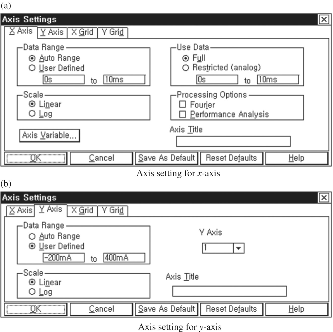
Figure H.9 Axis Settings dialog box
You can label the x‐/y‐axis by entering a title string into the Axis Title field in the Axis Settings dialog box for the x‐/y‐axis (Figure H.9(a)/(b)). You can also write a text string (name) and draw a line/arrow/box/circle on the graph by clicking Plot> Label>( Text| Line| Arrow| Box| Circle). You can see the Fourier spectra of signals plotted versus frequency in the Probe window just by clicking Trace> Fourier on the menu bar or the Fourier button on the toolbar.
H.4.4 Initial Transient Bias Point
The bias point, also referred to as the operating point, means the DC steady‐state values of voltages and currents obtained with every inductor/capacitor short‐/open‐circuited and every AC source removed. PSpice finds it not only in the Bias Point analysis but also in the Transient (Time Domain) analysis (in the name of the initial transient bias point) as long as the SKIPBP box (in the corresponding Simulation Settings dialog box) is unchecked (as default) and the ICs of inductors and capacitors are not specified. Hence, if you want the transient analysis (of a circuit containing inductors/capacitors) to start from some other ICs than the DC steady‐state values for inductor currents and capacitor voltages, check the SKIPBP box and specify the ICs in the spreadsheets of the inductors/capacitors if they are not zeros (see Exercise H.1).
To have the bias point analysis results displayed/removed on the schematic, you should click P Spice> Bias_Points>Enable_Bias_( Voltage| Current| Power)_Display on the menu bar or the corresponding button on the toolbar of the Capture window. To have the bias point analysis results printed in the output file, you should check the square box before ‘Include detailed bias point information for nonlinear controlled sources and semiconductors (/OP)’ in the Simulation Settings dialog box for bias point analysis or in the Transient Output File Options dialog box opened by clicking the Output File Options button in the Simulation Settings dialog box for transient analysis.
H.4.5 Viewing Output File and Netlist File
To see the simulation output file (Figure H.10), you should click P Spice>Vie w_Output_File on the menu bar of the Capture window or the View Simulation Output File button on the left side of the Probe window (Figure H.6(b)). The output file contains the contents of the netlist file named ‘schematic1.net’, which shows the detailed description of the circuit. You can also see the netlist file by clicking P Spice>Vie w_Netlist_File on the menu bar of the Capture window.
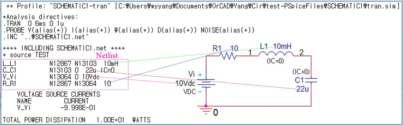
Figure H.10 An example of PSpice Simulation Output file.
H.5 Circuit Analysis Using OrCAD/Capture
H.5.1 DC Sweep Analysis
To practice the DC sweep analysis, let us get the common‐emitter (CE) collector characteristic curves of a bipolar junction transistor (BJT) by simulating the circuit of Figure H.11(a). For this job, we should draw the schematic and set the parameters in the Simulation Settings dialog box as depicted in Figure H.11(c) and (d). Then we will obtain the CE collector characteristic curves of the collector current iC versus the collector‐emitter junction voltage vCE for several values of the base current iB as depicted in Figure H.11(b).
As another application example of DC sweep analysis, we can draw the schematic of a CE transistor circuit as Figure H.12(a) and run it to get the curves of the B‐E junction voltage vBE, the base current iB, the collector current iC, the collector‐emitter junction voltage vCE, and the DC current gain hFE versus VBB as depicted in Figure H.12(b1)‐(b5). Instead of Voltage/Current Markers, we have clicked the Add Trace button on the tool bar of the Probe window to open the Add Traces dialog box and typed each target expression like ‘V(Q1:b)‐V(Q1:e)’ or ‘IC(Q1)/IB(Q1)’ (with no quotation mark) into the Trace Expression field to obtain these plots in the Probe window.
H.5.2 Transient Analysis
Figure H.13(a),(b), and (c) shows the schematic of an OP Amp circuit, the Simulation Settings dialog box for the time‐domain (transient) analysis, and the output waveforms obtained from the simulation, respectively. We may read the period of the output waveform either by using the cursor or by clicking the Evaluate Measurement button on the toolbar in the PSpice A/D (Probe) window to open the Evaluate Measurement window and by filling out the Trace Expression field as depicted in Figure H.13(d) to get the measurement result (Figure H.13(e)).
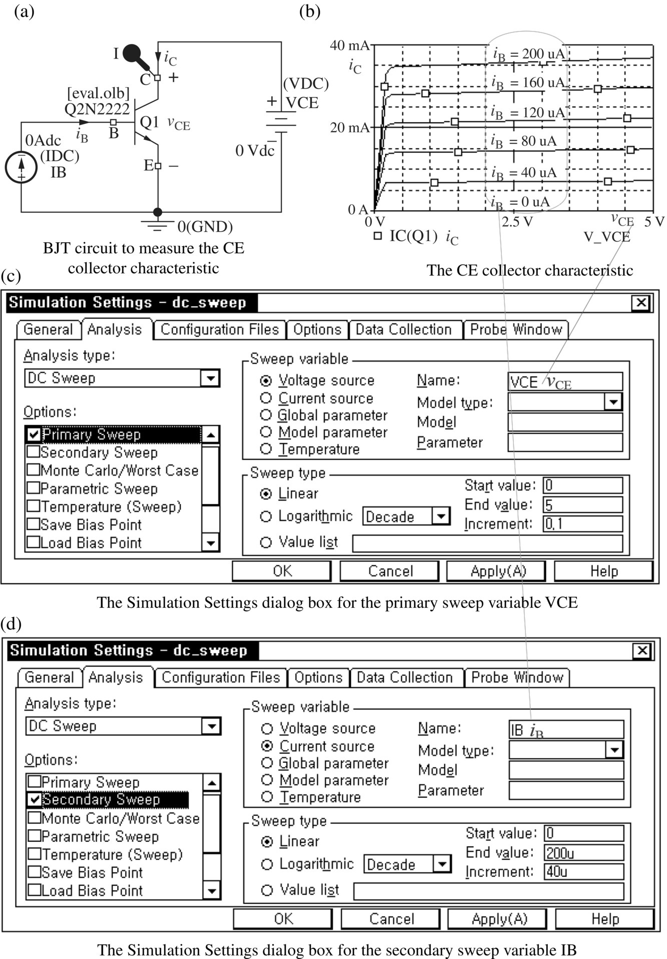
Figure H.11 Obtaining the common‐emitter (CE) collector characteristic curves (“BJT_CE0.opj”).
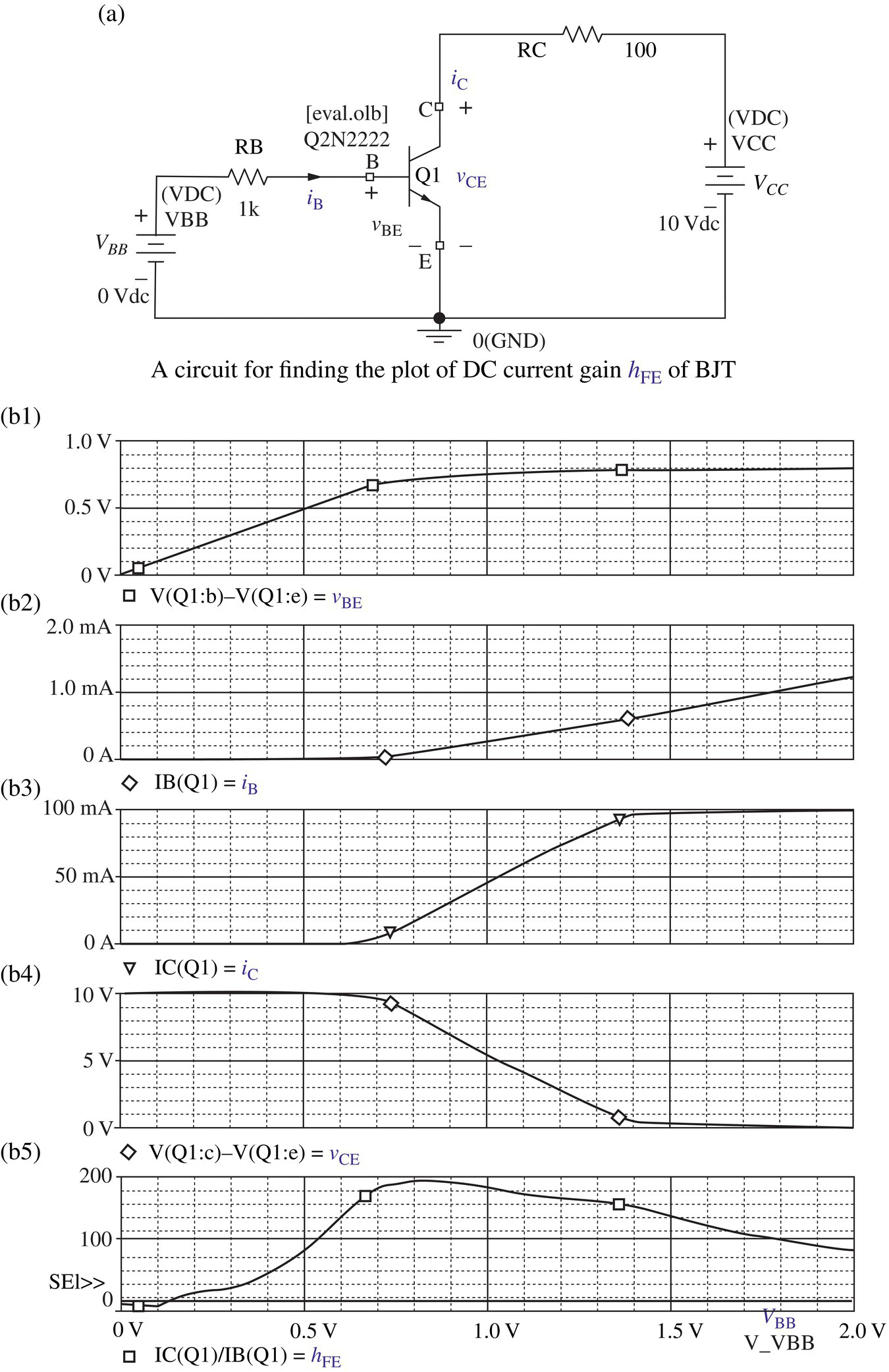
Figure H.12 Plots of vBE, iB, iC, vCE, and hFE versus VBB (“BJT_hFE.opj”).
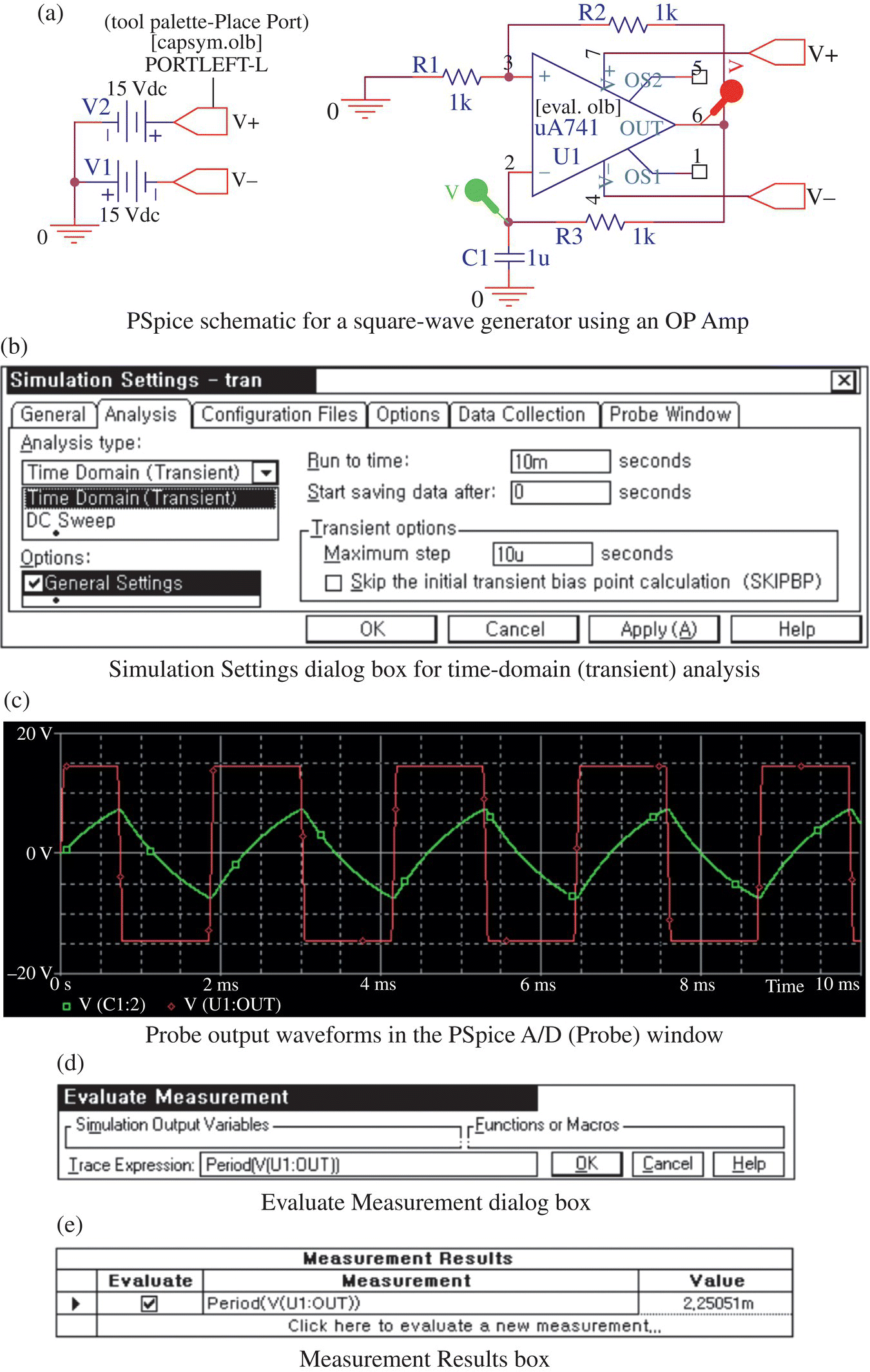
Figure H.13 PSpice simulation of an OP Amp circuit (“OPAmp_pos_feedback.opj”).
Figure H.14(a) shows a logic circuit for one‐bit full adder, which gets three inputs An, Bn, and Cn−1 (carry from bit n−1) and computes two outputs Sn (sum) and Cn (carry) as
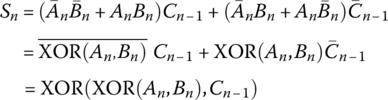
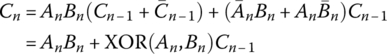
Figure H.14(b1)‐(b3) and (c) shows the Property Editor spreadsheets for each of the three inputs and the timing chart obtained from the transient analysis and seen in the PSpice A/D (Probe) window, respectively.

Figure H.14 PSpice simulation of a 1‐bit full adder (“full_adder.opj”).
H.5.3 AC Sweep Analysis
Figure H.15(a), (b), and (c) shows the schematic of an OP Amp circuit, the Simulation Settings dialog box for the frequency‐domain (AC sweep) analysis, and the frequency response curve obtained from the simulation. We may read the peak or center frequency fp and the lower/upper 3dB frequencies fl and fu of the band‐pass filter (BPF) by using the cursor or the Evaluate Measurement function as follows.
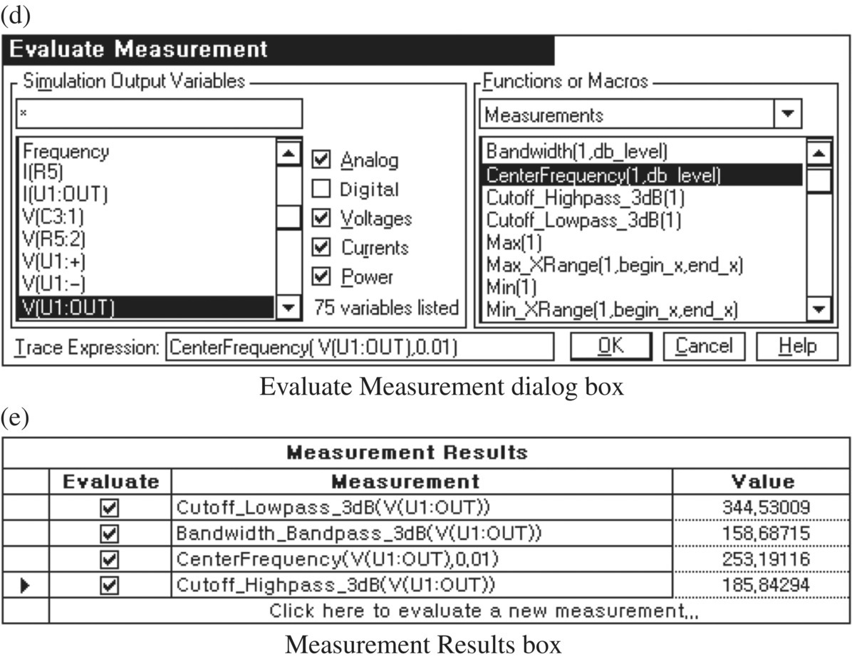
Figure H.15 PSpice simulation to get a frequency response (“OPAmp_filter_ac_sweep.opj”).
- To find the peak or center frequency fp at which the magnitude of the frequency response achieves its maximum, click the Toggle Cursor button to activate the cursor and then click the Cursor Max button on the toolbar of the Probe window, which will show you the cursor at the maximum together with the coordinates (fp, |G(j2πfp)|)=(254.097, 892.716m) in the Probe Cursor box (Figure H.15(c)).
- To find the two 3dB frequencies fl and fu at which the magnitude of the frequency response is (
 ) times its maximum, that is,
 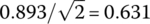 , let us draw a horizontal line of y = 0.631 by clicking the Add Trace button to open the Add Traces dialog box and typing ‘0.631’ (with no quotation mark) into the Trace Expression field. Then position the cursor at the two intersection points of the frequency response curve and the horizontal line of y = 0.631 by left‐/right‐clicking at the target points or pressing the (left or right) arrow/Shift + arrow key and read the coordinates of the two points from the Probe Cursor box, which will be

respectively (see Figure H.15(c)). It is also implied that the bandwidth is B = fu − fu ≈ 159.3 Hz.
- Once we have got the frequency response in the Probe window, we can easily find the center frequency, the 3 dB frequencies, and the bandwidth by using the Evaluate Measurement function. That is, you can click the Evaluate Measurement button to open the Evaluate Measurement dialog box and do the following:
- Fill out the Trace Expression field with
and click OK. Then you will see the value of the lower 3dB frequency in the Measurement Results box appearing (below the graph) at the bottom of the Probe window. Consecutively, click the bottom part of the Measurement Results box saying that
which will reopen the Evaluate Measurement dialog box. Then in the same way, you can type
one at a time, which will make the center frequency, the bandwidth, and the upper 3 dB frequency appear in the Measurement dialog box as illustrated in Figure H.15(e).
H.5.4 Parametric Sweep Analysis
While DC Sweep (Section H.5.1) and AC Sweep (Section H.5.3) analyses aim at observing the variation of the output versus the value of a DC source or the frequency of an AC source, Parametric Sweep analysis aims at observing the variation of the output versus the value of R, L, C, a model parameter, temperature, etc. Let us observe how the frequency response of the BPF in Figure H.16(a) varies with the value of R5 = 50, 100, and 150 kΩ by taking the following steps:
- Click the value of R5 (to be varied) and set it to {Rvar} (including the braces) in the schematic (Figure H.16(a)).
- Click the Place Part button on the tool palette of the Schematic window to open the Place Part dialog box, get PARAM (contained in the library ‘special.olb’), and click OK to place it somewhere in the schematic (Figure H.16(a)).

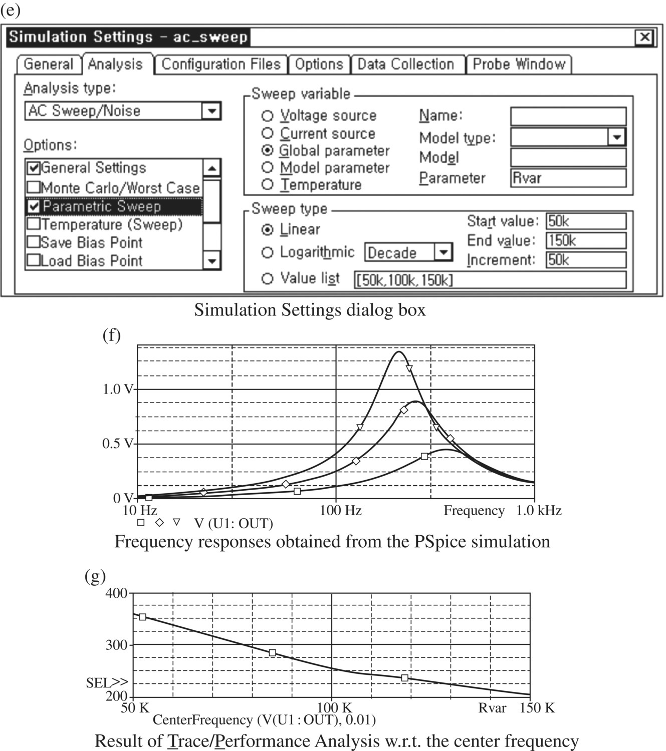
Figure H.16 Multiple AC Sweeps using Parametric Sweep (“OPAmp_filter_par.opj”).
- Double‐click the PARAMETERS placed in the schematic to open the Property Editor spreadsheet (Figure H.16(b)) and click the New Column button to open the Add New Column box (Figure H.16(c)), in which you can type Rvar and 100 into the Name and Value fields, respectively, where the numerical value entered as 100 here does not matter.
- Click the New Simulation Profile button to create a new simulation profile named, say, ‘AC_sweep’, click the Edit Simulation Profile button to open the Simulation Settings dialog box, and fill it out as depicted in Figure H.16(e), where the menu of Options is selected as Parametric Sweep, the Sweep variable is chosen to be Global parameter named ‘Rvar’, and the Sweep type is set to Linear with the Start value 50k, the End value 150k, and the Increment 50k. If the values of parameters do not form an arithmetic progression (with constant difference), you may type the list of the parameter values into the Value list field as illustrated in Figure H.16(e). Then click OK to close the Simulation Settings dialog box.
- Click the Voltage/Level Marker button to put the voltage probe pin at the OP Amp output node, click the Run button to perform the simulation, and see the multiple frequency curves as illustrated in Figure H.16(f).
- To see how the center frequency fp varies with the value of R5 = {Rvar}, click Trace/ Performance Analysis on the menu bar of the PSpice A/D (Probe) window to create an additional graph, click the Add Trace button to open the Add Traces dialog box, and fill out the Trace Expression field with
Then click OK to see the plot of fp versus R5 as depicted in Figure H.16(g).
H.5.5 Transient/Fourier Analysis
Figure H.17(a) shows the PSpice schematic of an RC circuit excited by a rectangular (square) wave voltage source of height ±Vm = ±π, period T = 2 [s], and duration (pulse width) D = 1 [s], where the voltage across the capacitor is taken as the output. To have the Fourier analysis results printed in the output file, we set the simulation profile and click the Output File Options button to open the Transient Output File Options dialog box, in which you are supposed to enter the fundamental frequency f0 = 1/T = 1/2 = 0.5 Hz, the number of harmonics which you want to observe, and the list of output variable(s) for Fourier analysis into the corresponding fields, say, as illustrated in Figure H.17(b). Now, we put the Voltage/Level probe pins at the input/output nodes, click the Run button to perform the simulation, and see the input/output waveforms in the Probe window as illustrated in Figure H.17(c). Whenever you want to see the spectra of the signals (Figure H.17(d)) whose waveforms are shown in the Probe window, you just click the (toggle) fast Fourier transform (FFT) button on the toolbar. You can also view the output file as shown in Figure H.17(e) by clicking (selecting) PSpice/View_Output_File on the top menu bar and pull‐down menu in the Capture window or View/Output_Fi le on the menu bar or the View_Simulation_Output_File button on the left toolbar of the Probe window.
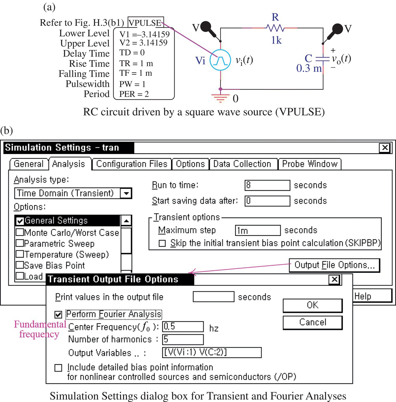
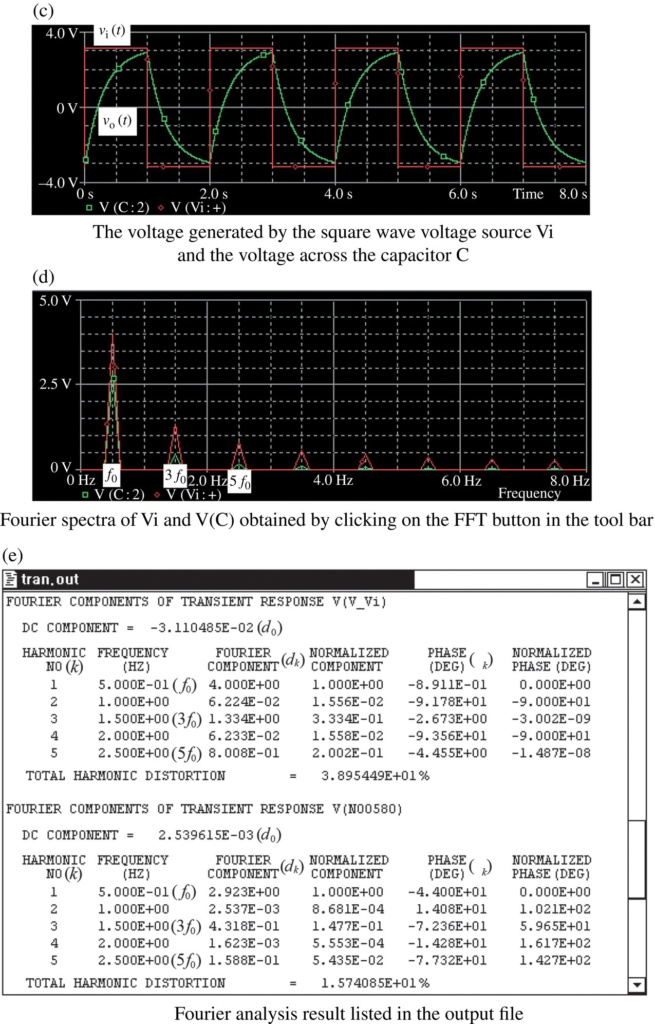
Figure H.17 Example of Fourier analysis using PSpice (“RC_pulse_Fourier.opj”).
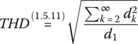
Note that based on the Fourier analysis results printed in the output file, we can write the Fourier series representation of the input and output signals as
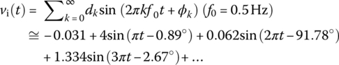
and the total harmonic distortion (THD) is defined as
H.5.6 Bias Point/DC Sensitivity and Transfer Function Analysis
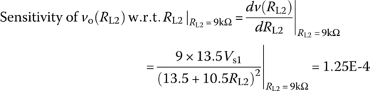
Figure H.18(a1) and (a2) shows two interface circuits each of which takes on a duty of transferring the DC voltage of 9 V from the 12 V source (with the source impedance of 1.5 kΩ) to a 9 kΩ resistor. Figure H.18(b) shows the Simulation Settings dialog box to be set for DC Sensitivity analysis of the output voltage w.r.t. the load resistance and Transfer Function analysis to find the DC gain and the input/output resistances, where ‘V(RL2)’ should be typed into the Output and To_Output variable fields instead of ‘V(RL1)’ for the analysis of circuit (a2). Figure H.18(c1)/(c2) and (d1)/(d2) shows the results of the DC Sensitivity and Transfer Function analyses for the two circuits (a1)/(a2), that can be seen from the output file.
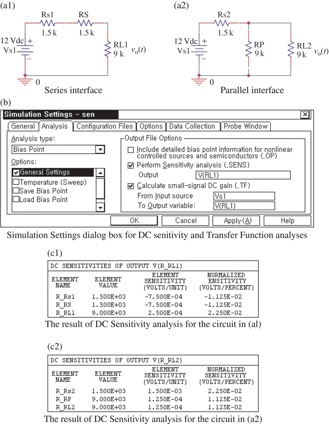
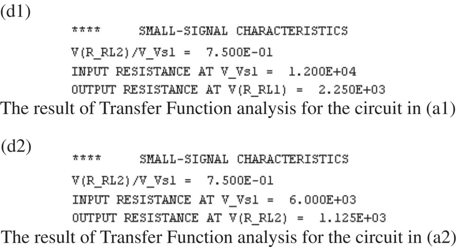
Figure H.18 DC Sensitivity and Transfer Function analyses (“test_sensitivity.opj”).
In order to understand and verify these analysis results, let us find the sensitivities, DC gains, and the input/output impedances by using an analytical method as follows:
- For the circuit (a), we have
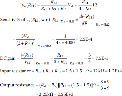
- For the circuit (b), we have


H.5.7 Monte Carlo Analysis
Figure H.19(a) shows the Capture window, which has the schematic of a CE BJT amplifier circuit. To see how the output voltage varies with the ±20% change of the load resistance RL(RL) and the ±50% change of the CE forward current gain βF, let us take the following steps of Monte Carlo/Worst‐Case analysis presented by PSpice.
- Create a PSpice project, say, named ‘BJT_CE_Amp1_mon.opj’ and draw a schematic in the Schematic Editor Window as depicted in Figure H.19(a).
- Click the BJT(Q1) for selection so that it will be pink‐hot and boxed by a dotted‐line rectangle. Then click Edit/PSpice Model on the menu bar to open the PSpice Model Editor Window (Figure H.19(b)), in which you can type ‘Dev=50%’ (including the first blank space, but without the single quotation marks) just after ‘Bf=255.9’ in the model statement. Then press the ‘^s’ key to save the PSpice model for the device Q2N2222 placed in the schematic and click on x to close the Editor Window.
- Click the load resistor RL for selection and press the ‘Del’ key to delete it. Then click the Place Part button to open the Place Part dialog box, search/select Rbreak[breakout.olb], and click OK to place it in place of RL.
- Click the load resistor RL (having the part name ‘Rbreak’) for selection, click Edit/PSpice Model on the menu bar to open the PSpice Model Editor Window (Figure H.19(b)), in which you can change the model name from Rbreak for RMonte1, and type ‘Dev=20%’ just after ‘R=1’ (the default value of the resistance) in the model statement. Then press the ‘^s’ key to save the PSpice model for the device RMonte1 placed in the schematic and click on x to close the Editor Window.
- Click the New Simulation Profile button on the toolbar to create a new simulation profile named, say, ‘tran’ and then click the Edit Simulation Settings button to open the Simulation Settings dialog box, in which you can do the following:
- Set the Analysis type and Run_to_time to ‘Time Domain (Transient)’ and ‘2ms’ respectively.
- Select (click) Monte Carlo/Worst Case from the Options menu, select Monte Carlo from the upper‐right menu, type ‘V(RL:2)’ into the Output variable field, and type ‘5’ into the Number of Runs field, … as depicted in Figure H.19(c).
- Then click OK to close the Simulation Settings dialog box.
- Click the Voltage/Level Marker button to place two voltage probe pins, one at the upper node of RL and one at the + terminal of the sinusoidal input voltage source VSIN.
- Click the Run button to perform the simulation to see the input/output waveforms in the Probe window as depicted in Figure H.19(d). You can also click the View Simulation Output File button to view the output file as illustrated in Figure H.19(e).
- Click the Edit Simulation Settings button to reopen the Simulation Settings dialog box (Figure H.19(f)), in which you can do the following:
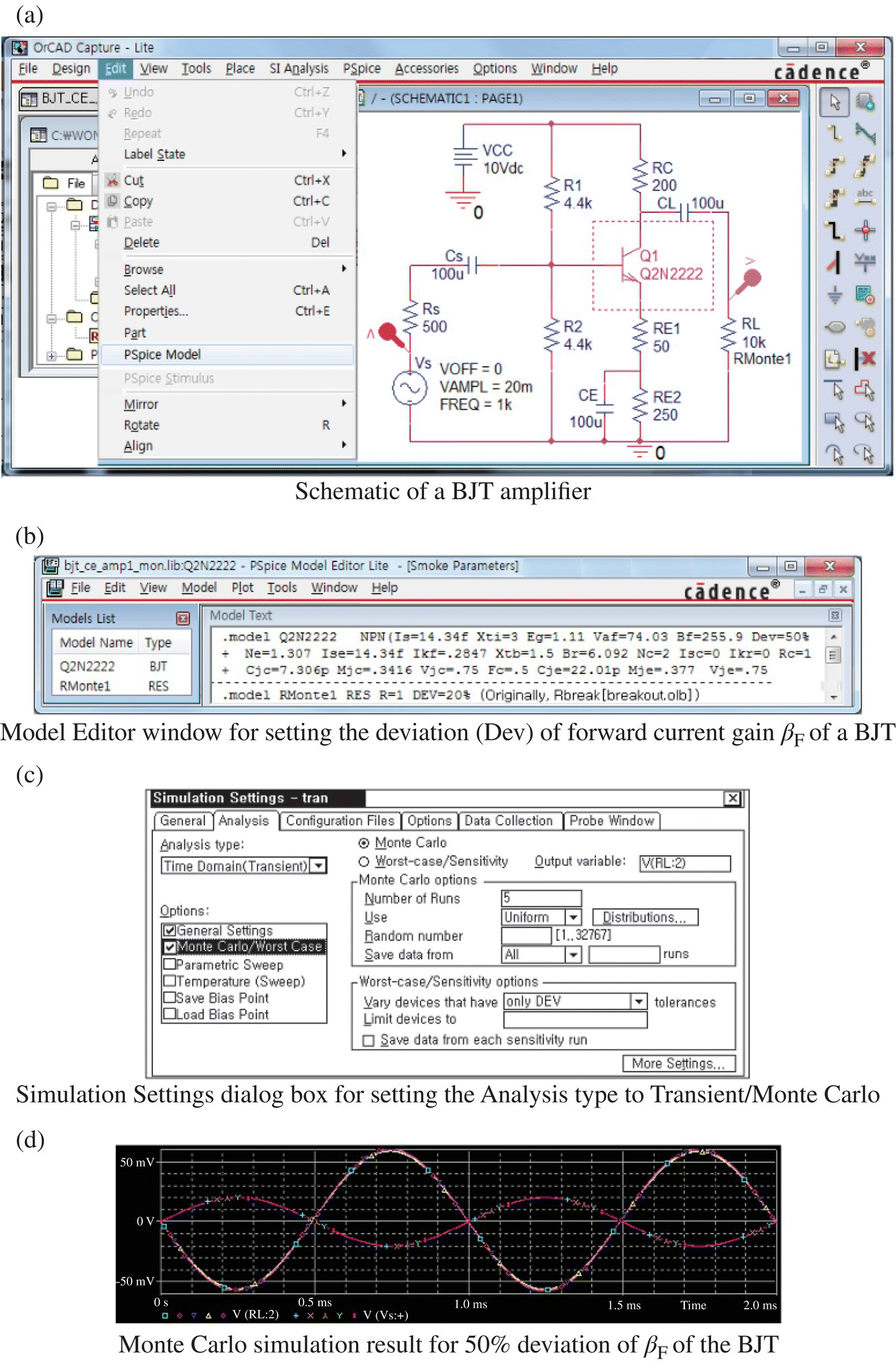
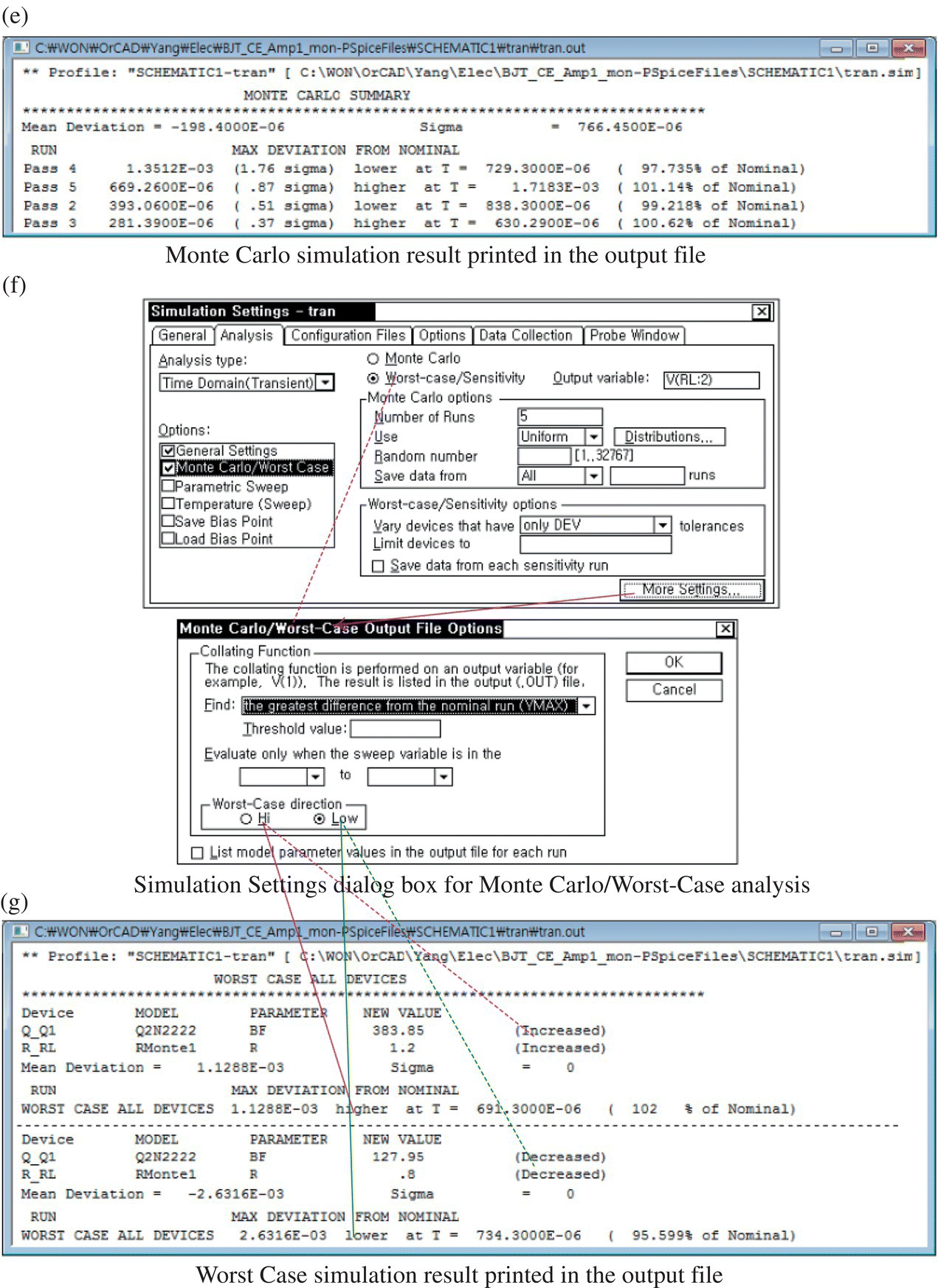
Figure H.19 Example of Monte Carlo simulation (“BJT_CE_amp1_mon.opj”).
- Select Monte Carlo/Worst Case in the Options menu, select Worst‐Case/Sensitivity from the upper‐right menu, and select ‘only DEV’ in the tolerance field of the Worst‐Case/Sensitivity options box.
- Click the More Settings button to open the Monte Carlo/Worst‐Case Output File Options dialog box, in which you can select High or Low in the Worst‐Case direction box.
- Click OK to close the Monte Carlo/Worst‐Case Output File Options dialog box and then click OK to close the Simulation Settings dialog box.
- Click Run to perform the simulation and see the input/output waveforms in the Probe window. You can also click the View Simulation Output File button to view the output file as illustrated in Figure H.19(g), the contents of which depends on which of High and Low has been selected as the Worst‐Case direction.
H.5.8 AC Sweep/Noise Analysis
Figure H.20(a) and (b) shows the PSpice schematic of a CE BJT amplifier circuit and the Simulation Settings dialog box for AC Sweep/Noise analysis, respectively. With the simulation profile made by setting the Simulation Settings dialog box as illustrated in Figure H.20(b) and the Voltage/Level probe pins attached at the upper nodes of RL and Vs, we can run the PSpice simulation to get the input and output noises for the specified frequency range of 10 Hz∼10 MHz as depicted in Figure H.20(c), where the output noise is the root‐mean‐square (rms) sum of all the device contributions propagated to a specified output and the input noise is the equivalent noise that would be needed at the input source to generate the calculated output noise in an ideal (noiseless) circuit. You can also view the output file (Figure H.20(d)) containing every device noise, that is the noise contribution propagated to the specified output from every resistor and semiconductor device in the circuit. Note that the three frequencies f = 10, 104, and 107 Hz at which the noise analysis has been done are extracted with the interval of 300 points from the total 601 frequency points (100 points per decade) from 10 Hz to 10 MHz as specified in the Simulation Settings dialog box (Figure H.20(b)).
H.6 How to Save a Project as another Project
To save a current (existing) project as another project (with a different file name), click on the Project Manager tab to activate (highlight) the corresponding Project Manager window, select File>Save_Project_As from the top menu bar to open the Save Project dialog box as depicted in Figure H.22, specify a location, enter a new project name, and click OK.
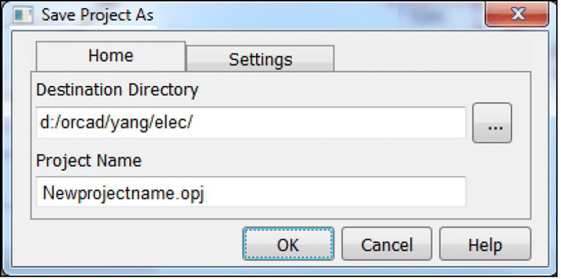
Figure H.22 Save Project dialog box.