Appendix J
Diode/BJT/FET
J.1 Diode
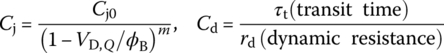
The junction (depletion) and diffusion capacitances are
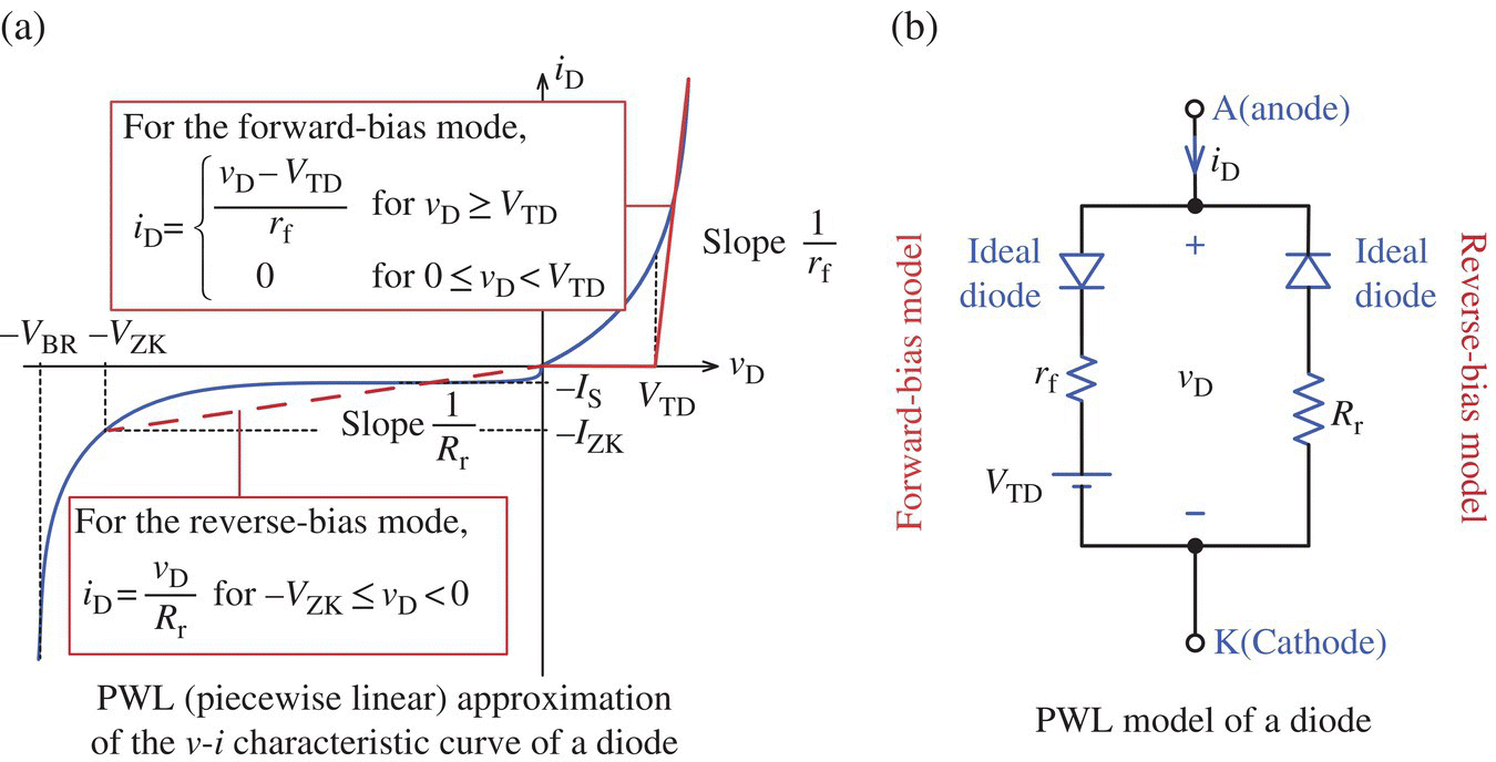
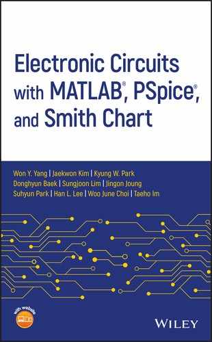
Figure J.1 Piecewise linear current (PWL) approximation of the v‐i characteristic curve of a diode and the corresponding model.
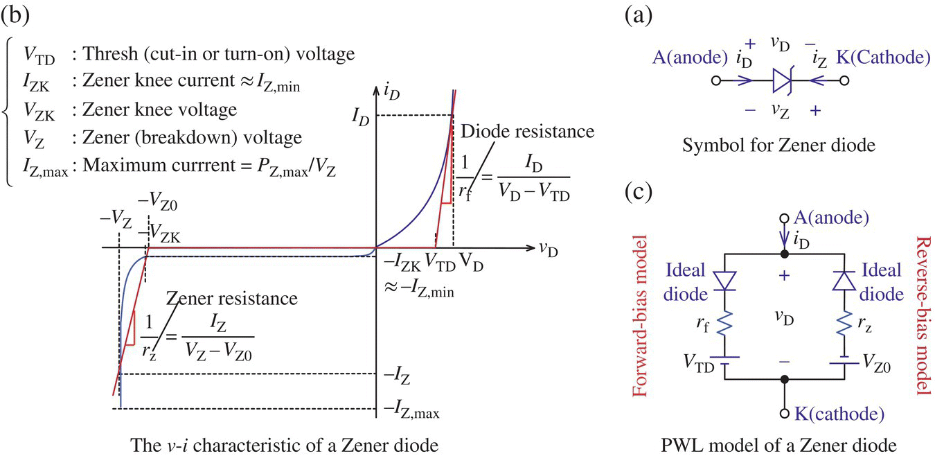
Figure J.2 Symbol, v‐i characteristic, and PWL model of a Zener diode.
Figure J.3 High‐frequency AC (small‐signal) model of a diode.
| SPICE name | Model parameter | Default value |
| IS | Transport saturation current Is | 10−14 |
| RS | Ohmic (series) resistance Rs | 0 [Ω] |
| N | Emission (ideality) coefficient η | 1 |
| CJO | Zero‐bias junction capacitance Cj0 | 0 |
| VJ | PN junction (built‐in) potential ϕB | 1 [V] |
| MJ | PN grading coefficient m | 0.5 |
| TT | Transit time τt | 0 [s] |
| BV | Reverse breakdown voltage VZ | ∞ [V] |
| IBV | Reverse breakdown current IZ | 10−3 |
J.2 BJT (Bipolar Junction Transistor)
- gm: transconductance (gain)
(J.2)
 (J.3)
(J.3)
- Cbe/Cbc: zero‐bias B‐E/B‐C junction capacitances
(J.4)
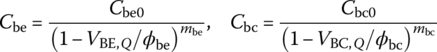
- Cbe0(CJE)/Cbc0(CJC): zero‐bias B‐E/B‐C junction capacitances
- VBE,Q/VBC,Q: quiescent B‐E/B‐C voltages [V]
- mbe(MJE)/mbc(MJC): B‐E/B‐C grading coefficient
- ϕbe(VJE)/ϕbc(VJC): B‐E/B‐C built‐in potential
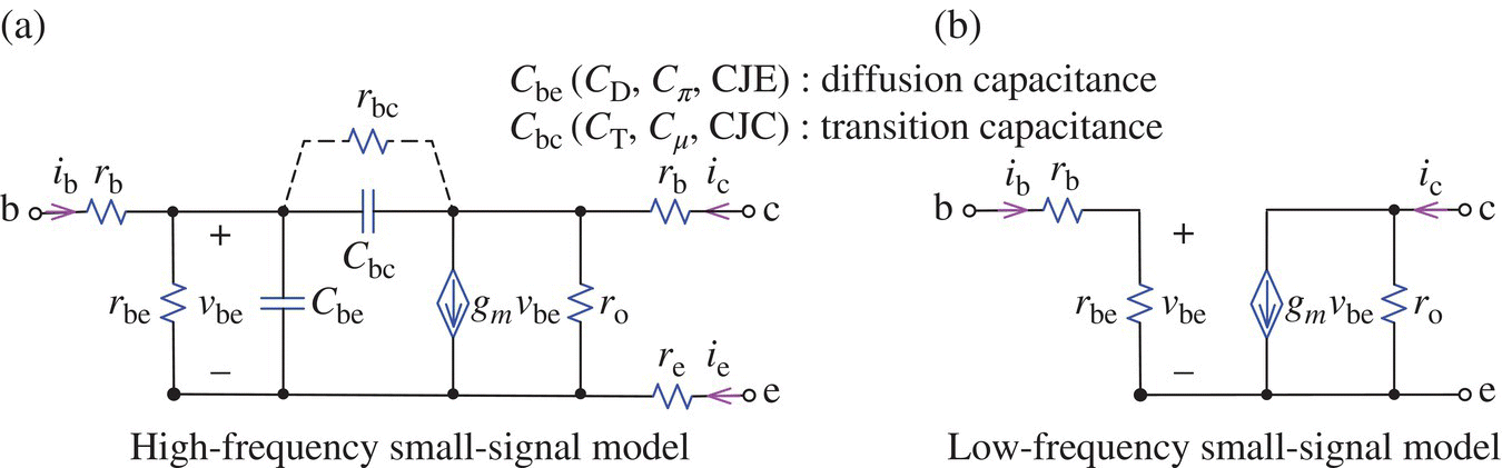
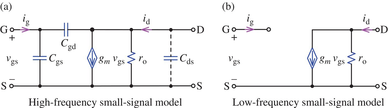
Figure J.4 Hybrid‐π small‐signal models of NPN‐BJT with or without frequency dependence.
| SPICE name | Model parameter | Default value |
| BF | Forward active current gain βF | 100 |
| BR | Reverse active current gain βR | 1 |
| IS | Transport saturation current Is | 10−16 |
| ISC | B‐C leakage saturation current Isc | 0 |
| CJE | B‐E zero‐bias junction (depletion) capacitance Cbe0 | 0 |
| CJC | B‐C zero‐bias junction (depletion) capacitance Cbc0 | 0 |
| VJE | B‐E built‐in potential ϕbe | 0.75 [V] |
| VJC | B‐C built‐in potential ϕbc | 0.75 [V] |
| VAF | Forward mode Early voltage | ∞ [V] |
| VAR | Reverse mode Early voltage | ∞ [V] |
| NF | Forward ideality factor (current emission coefficient) | 1 |
| NR | Reverse ideality factor (current emission coefficient) | 1 |
| MJE | B‐E capacitance exponent mbe | 0.33 |
| MJC | B‐C capacitance exponent mbc | 0.33 |
| RB | Base resistance rb | 0 [Ω] |
| RE | Emitter resistance re | 0 [Ω] |
| RC | Collector resistance rc | 0 [Ω] |
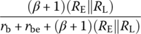
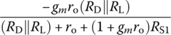
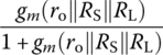
Table J.3 Characteristics of CE/CC/CB amplifiers (β = gmrbe = (IC,Q/VT)rbe).
| CE | CC | CB | |
| Ri | RB||{rb+rbe+(β+1)RE1}(3.2.1) | RB||{rb+rbe+(β+1)(RE||RL)}(3.2.5) | |
| Ro | RC||ro≈RC(3.2.4) | RC||ro1(3.2.12) | |
| Av | 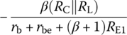 (3.2.3) (3.2.3) |
 (3.2.7) (3.2.7) |
|
| Ai |  |

J.3 FET (Field Effect Transistor)
The body effect or substrate sensitivity[J-1] of the threshold voltage Vt is described by
The gate‐source and gate‐drain capacitances are modeled as voltage‐dependent capacitances:
| SPICE name | Model parameter | Default value |
| VTO | Zero‐bias threshold voltage Vt0 | 0 [V] |
| KP | Transconductance parameter Kp = μpCOX(W/L) | 2 × 10⁻⁵ [A/V2] |
| GAMMA | Bulk threshold parameter γ | 0 [V1/2] |
| PHI | Surface (bulk) potential ϕ | 0.6 [V] |
| LAMBDA | Channel length modulation parameter λ | 0 [V−1] |
| PB | Built‐in potential for the bulk (substrate) junction Vb | 0.8 [V] |
| CGSO | Gate‐source overlap capacitance per meter channel length Cgs0 | 0 [F/m] |
| CGDO | Gate‐drain overlap capacitance per meter channel length Cgd0 | 0 [F/m] |
| CGBO | Gate‐bulk overlap capacitance per meter channel length Cgb0 | 0 [F/m] |
| MJ | Bulk junction bottom grading coefficient m | 0.5 |
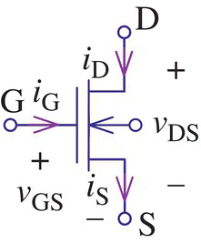
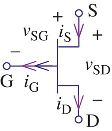
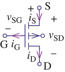
Table J.5 Circuit symbols and i‐v relationships of JFET and MOSFET.
| FET type | n‐Channel | p‐Channel | ||||
| JFET | Enhancement MOSFET | Depletion MOSFET | JFET | Enhancement MOSFET | Depletion MOSFET | |
| Circuit symbols | 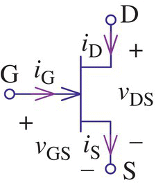 |
 |
 |
 |
 |
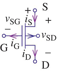 |
| Thresholdvoltage Vt | − | + | − | + | − | − |
| Conductionconstant Kp | Process conduction parameter |
Process conduction parameter |
||||
| Turn‐on condition | vGS > Vt and vDS > 0 | vSG > ∣Vt ∣and vSD > 0 | ||||
| Triode region (Ohmic mode) | vGD = vG − vD > Vt > 0 | vDG = vD − vG > ∣Vt∣ | ||||
with overdrive voltage vOV = vGS − Vt |
with overdrive voltage vOV = vSG − ∣Vt∣ |
|||||
| Saturation region (Pinch‐off mode) | vGD = vG − vD ≤ Vt | vDG = vD − vG ≤ ∣Vt∣ | ||||
| iD ≅ Kp(vGS − Vt)2/2 | iD ≅ Kp(vSG − ∣Vt∣)2/2(4.1.13b) | |||||

where Cgs0/Cgd0: zero‐bias gate‐source/gate‐drain junction capacitances, respectively, VGS,Q/VGD,Q [V]: quiescent gate‐source/gate‐drain voltages, respectively, m(MJ): gate p‐n grading coefficient (SPICE default = 0.5), and Vb(PB): gate junction (barrier) potential, typically 0.6 V (SPICE default = 1 V).
 (4.2.11)
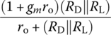 (4.2.16)