1
Load Line Analysis and Fourier Series
1.1 Load Line Analysis
The v-i characteristic of a nonlinear resistor such as a diode or a transistor is often described by a curve on the v-i plane rather than by a mathematical relation. The v-i characteristic curve can be obtained by using a curve tracer for nonlinear resistors. To analyze circuits containing a nonlinear resistor, we should use the load line analysis. To grasp the concept of the load line, consider the graphical analysis of the circuit in Figure 1.1(a), which consists of a linear resistor R1, a nonlinear resistor R2, a DC voltage source Vs, and an AC voltage source of small amplitude vδ ≪ Vs. Kirchhoff's voltage law (KVL) can be applied around the mesh to yield the mesh equation as
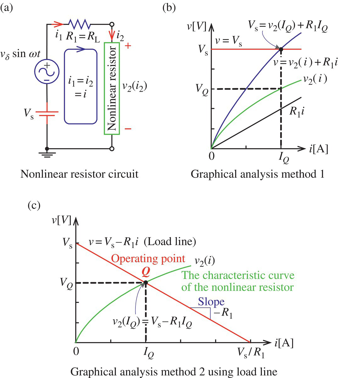
Figure 1.1 Graphical analysis of a linear/nonlinear resistor circuit.
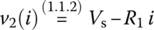
where the v-i relationship of R2 is denoted by v2(i) and represented by the characteristic curve in Figure 1.1(b). We will consider a graphical method, which yields the quiescent, operating, or bias point Q = (IQ, VQ), that is, a pair of the current through and the voltage across R2 for vδ = 0.
Since no specific mathematical expression of v2(i) is given, we cannot use any analytical method to solve this equation and that is why we are going to resort to a graphical method. First, we may think of plotting the graph for the LHS (left‐hand side) of Eq. (1.1.1) and finding its intersection with a horizontal line for the RHS (right‐hand side), that is, v = Vs as depicted in Figure 1.1(b). Another way is to leave only the nonlinear term on the LHS and move the other term(s) into the RHS to rewrite Eq. (1.1.1) as
and find the intersection, called the operating point and denoted by Q (quiescent point), of the graphs for both sides as depicted in Figure 1.1(c). The straight line with the slope of −R1 is called the load line. This graphical method is better than the first one in the aspect that it does not require us to plot a new curve for v2(i) + R1i. That is why it is widely used to analyze nonlinear resistor circuits in the name of ‘load line analysis’. Note the following:
- Most resistors appearing in this book are linear in the sense that their voltages are linearly proportional to their currents so that their voltage-current relationships (VCRs) are described by Ohm's law
(1.1.3)and consequently, their v-i characteristics are described by straight lines passing through the origin with the slopes corresponding to their resistances on the i-v plane. However, they may have been modeled or approximated to be linear just for simplicity and convenience, because all physical resistors more or less exhibit some nonlinear characteristic. The problem is whether or not the modeling is valid in the range of practical operation so that it may yield the solution with sufficient accuracy to serve the objective of analysis and design.

- A curve tracer is an instrument that displays the v-i characteristic curve of an electric element on a cathode‐ray tube (CRT) when the element is inserted into an appropriate receptacle.
1.1.1 Load Line Analysis of a Nonlinear Resistor Circuit
Consider the circuit in Figure 1.1(a), where a linear load resistor R1 = RL and a nonlinear resistor R connected in series are driven by a DC voltage source Vs in series with a small‐amplitude AC voltage source producing the virtual voltage as
The VCR v(i) of the nonlinear resistor R is described by the characteristic curve in Figure 1.2.
As depicted in Figure 1.2, the upper/lower limits as well as the equilibrium value of the current i through the circuit can be obtained from the three operating points, that is, the intersections (Q1, Q, and Q2) of the characteristic curve with the following three load lines.
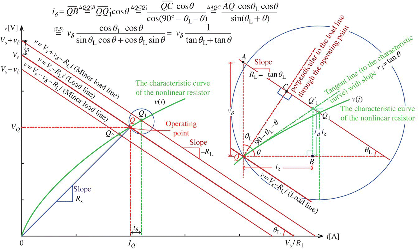
Figure 1.2 Variation of the voltage and current of a nonlinear resistor around the operating point Q.
Although this approach gives the exact solution, we gain no insight into the solution from it. Instead, we take a rather approximate approach, which consists of the following two steps.
- Find the equilibrium (IQ, VQ) at the major operating point Q, which is the intersection of the characteristic curve with the DC load line (1.1.5b).
- Find the two approximate minor operating points
 and
and  from the intersections of the tangent to the characteristic curve at Q with the two minor load lines (1.1.5a) and (1.1.5c).
Then we will have the current as
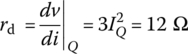
With the dynamic, small‐signal, or AC resistance rd defined to be the slope of the tangent to the characteristic curve at Q as

let us find the analytical expressions of IQ and iδ in terms of Vs and vδ, respectively. Referring to the encircled area around the operating point in Figure 1.2, we can express iδ in terms of vδ as
This corresponds to approximating the characteristic curve in the operation range by its tangent at the operating point. Noting that
- the load line and the tangent to the characteristic curve at Q are at angles of (180° − θL) and θ to the positive i‐axis,
- the slope of the load line is tan (180° − θL) =−tan θL and it must be −RL, which is the proportionality coefficient in i of the load line Eq. (1.1.2); tan θL =RL, and
- the slope of the tangent to the characteristic curve at Q is the dynamic resistance rd defined by Eq. (1.1.7); tan θ = rd,
we can write Eq. (1.1.8) as
Now we define the static or DC resistance of the nonlinear resistor R to be the ratio of the voltage VQ to the current IQ at the operating point Q as
so that the DC component of the current, IQ, can be written as
Finally, we combine the above results to write the current through and the voltage across the nonlinear resistor R as follows.
This result implies that the nonlinear resistor exhibits twofold resistance, that is, the static resistance Rs to a DC input and the dynamic resistance rd to an AC input of small amplitude. That is why rd is also called the (small‐signal) AC resistance, while Rs is called the DC resistance.
1.1.2 Load Line Analysis of a Nonlinear RL circuit
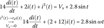
As an example of applying the load line analysis for a nonlinear first‐order circuit, consider the circuit of Figure 1.3.1(a), which consists of a nonlinear resistor, a linear resistor R = 2 Ω, and an inductor L = 14 H, and is driven by a DC voltage source of Vs = 12 V and an AC voltage source vδ sin ωt = 2.8 sin t[V]. The v-i relationship of the nonlinear resistor is v(i) = i3 and described by the characteristic curve in Figure 1.3.1(b). Applying KVL yields the following mesh equation:
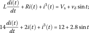

Figure 1.3.1 A nonlinear RL circuit and its load line analysis.
First, we can draw the load line on the graph of Figure 1.3.1(b) to find the operating point Q from the intersection of the load line and the v-i characteristic curve of the nonlinear resistor. If the function v(i) = i3 of the characteristic curve is available, we can also find the operating point Q as the DC solution to Eq. (1.1.15) by removing the AC source and the time derivative term to write
and solving it as
Eq. (1.1.16) can be solved by running the following MATLAB statements:
>>eq_dc=@(i)2*i+i.^3-12; I0=0; IQ=fsolve(eq_dc,I0)
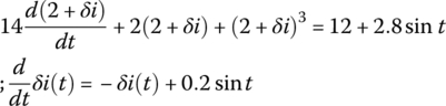
Then, as a preparation for analytical approach, we linearize the nonlinear differential equation (1.1.15) around the operating point Q by substituting i = IQ + δi = 2 + δi into it and neglecting the second or higher degree terms in δi as
Note that we can set the slope of the characteristic curve as the dynamic resistance rd of the nonlinear resistor:
and apply KVL to the circuit with the DC source Vs removed and the nonlinear resistor replaced by rd to write the same linearized equation as Eq. (1.1.18):
We solve the first‐order linear differential equation with zero initial condition δi(0) = 0 to get δi(t) by running the following MATLAB statements:
>>syms sdIs=2.8/(s^2+1)/14/(s+1); dit_linearized=ilaplace(dIs)dit1_linearized=dsolve('Dx=-x+0.2*sin(t)','x(0)=0') % Alternatively
This yields
dit_linearized = exp(-t)/10 - cos(t)/10 + sin(t)/10
which means
We add this AC solution to the DC solution IQ to write the approximate analytical solution for i(t) as
Now, referring to Appendix D, we use the MATLAB numerical differential equation (DE) solver ‘ode45()’ to solve the first‐order nonlinear differential equation (1.1.15) by defining it as an anonymous function handle:
>>di=@(t,i)(12+2.8*sin(t)-2*i-i.^3)/14; % Eq. (1.1.15)
and then running the following MATLAB statements:
>>i0=IQ; tspan=[0 10]; % Initial value and Time span[t,i_numerical]=ode45(di,tspan,i0); % Numerical solution
We can also plot the numerical solution together with the analytical solution as black and red lines, respectively, by running the following MATLAB statements:
>>i_linearized=eval(IQ+dit_linearized); % Analytical solution (1.1.22)plot(t,i_numerical,'k', t,i_linearized,'r')
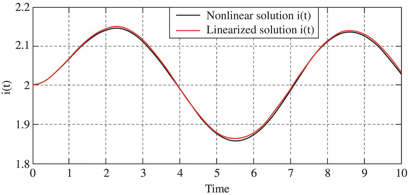
Figure 1.3.2 The linearized solution and nonlinear solution for the nonlinear RL circuit of Figure 1.3.1.
This will yield the plots of the numerical solution i(t) and the approximate analytical solution (1.1.22) for the time interval [0,10 s] as depicted in Figure 1.3.2.
Overall, we can run the above MATLAB script “elec01f03.m” to get Figure 1.3.1(b) (the load line together with the characteristic curve) and Figure 1.3.2 (the numerical nonlinear solution together with the analytical linearized solution) together.
1.2 Voltage-Current Source Transformation
Two electric circuits are said to be externally equivalent with respect to a pair of terminals if their terminal voltage-current relationships are identical so that they are indistinguishable from outside. The source transformation refers to the conversion of a voltage source in series with an element like a resistor (Figure 1.4(a)) to a current source in parallel with the element (Figure 1.4(b)), or vice versa in such a way that the two circuits are (externally) equivalent w.r.t. their terminal characteristics. What is the relationship among the values of the voltage source Vs, the current source Is, the series resistor Rs, and the parallel resistor Rp required for the external equivalence of the two source models? To find it out, we write the VCR of each circuit as
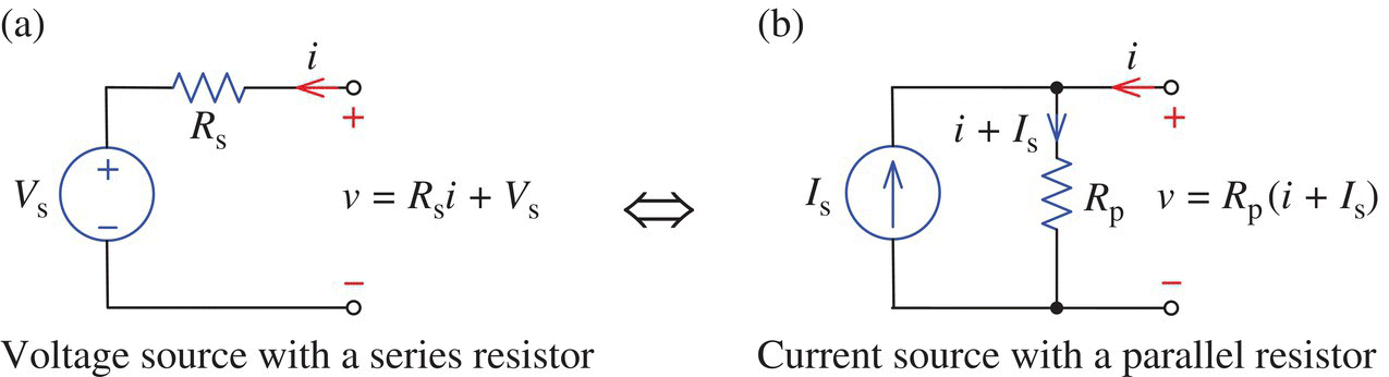
Figure 1.4 Equivalence of voltage and current sources.
where the current through Rp is found to be (i + Is) by applying KCL at the top node of the resistor Rp in Figure 1.4(b). In order for these two polynomial equations (in i) to be identical for any value of v and i, their coefficients (including the constant term) should be the same:
This source equivalence condition is used for voltage‐to‐current or current‐to‐voltage source transformation.
1.3 Thevenin/Norton Equivalent Circuits
Thevenin's theorem says that any network consisting of linear elements and independent/dependent sources as shown in Figure 1.5(a) may be replaced at a pair of its terminals (nodes) by the Thevenin equivalent circuit, which consists of a single element of impedance ZTh in series with a single independent voltage source VTh (see Figure 1.5(b)), where the values of ZTh and VTh are determined as follows:
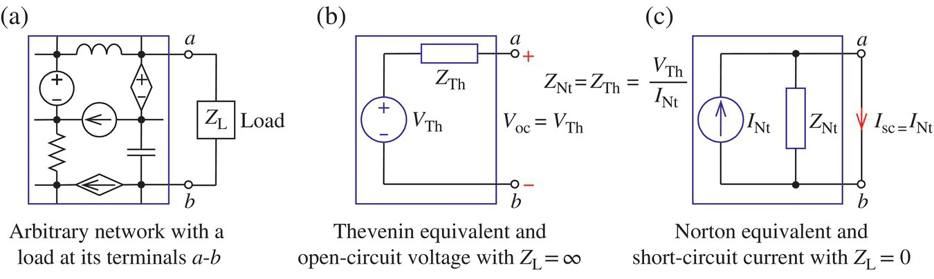
Figure 1.5 Thevenin/Norton equivalents of an arbitrary circuit seen from terminals a to b.
- T1. Thevenin eqavuivalent voltage source VTh:
- The open‐circuit voltage across the terminals, that is, the voltage across the open‐circuited terminals a‐b (with ZL = ∞).
- T2. Thevenin equivalent impedance ZTh:
- The equivalent impedance of the circuit (with all the independent sources removed) seen from the terminals a‐b, where an impedance is a ‘generalized’ resistance.
Norton's theorem says that any linear network may be replaced at a pair of its terminals by the Norton equivalent circuit, which consists of a single element of impedance ZNt in parallel with a single independent current source INt (see Figure 1.5(c)), where the values of ZNt and INt are determined as follows:
- N1. Norton equivalent current source INt:
- The short‐circuit current through the terminals, that is, the current through the short‐circuited terminals a‐b (with ZL = 0).
- N2. Norton equivalent impedance ZNt:
- The equivalent impedance of the circuit (with all the independent sources removed) seen from the terminals a‐b
Since Thevenin and Norton equivalents are equivalent in representing a linear circuit seen from a pair of two terminals, one can be obtained from the other by using the source transformation introduced in Section 1.2. This suggests another formula for finding the equivalent impedance as
Note that we should find the equivalent impedance after removing every independent source, that is, with every voltage/current source short‐/open‐circuited. For networks having no dependent source, the series/parallel combination and Δ‐Y/Y‐Δ conversion formulas often suffice for the purpose of finding the equivalent impedance. For networks having dependent sources, we should apply a test voltage source VT across the terminals, measure the current IT through the terminals (see Figure 1.6(a)), and write down the relationship between VT and IT as

Figure 1.6 One‐shot method for obtaining Thevenin equivalent.
In this relationship, we find the value of the equivalent impedance ZTh from the proportionality coefficient of the term in IT, and the equivalent source VTh from the constant term independent of IT. This suggests a one‐shot method of finding the values of the equivalent impedance ZTh and the equivalent source VTh or INt at a time. This one‐shot method of finding the equivalent may be applied for any linear networks with or without independent/dependent sources. Another way to find the equivalent circuit is to apply a test current source IT through the terminals (see Figure 1.6(b)), measure the voltage VT across the terminals, and write down the relationship between VT and IT as Eq. (1.3.2).
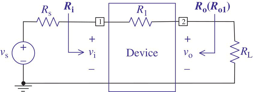
Figure 1.10 Input resistance, output resistance, and voltage gain for Example 1.4
Figure 1.11 Miller's theorem.
1.4 Miller's Theorem
Miller's theorem states that an element of impedance Z connected between two nodes 1 and 2 as shown in Figure 1.11(a), each with node voltage V1 and V2 = AvV1, respectively, can be replaced by an equivalent consisting of two impedances Z1 and Z2:
each of which is connected between the nodes 1/2 and a common node 0 as shown in Figure 1.11(b). It can easily be shown that the two circuits of Figure 1.11(a) and (b) are equivalent both from terminals 1 to 0 and 2 to 0. If the element is a capacitor of impedance Z = 1/sC, the equivalent capacitances seen from terminals 1 to 0 and 2 to 0 will be
Here, C1 is referred to as the Miller (effective) capacitance where (1 − Av) is called the Miller multiplier and the increase in the equivalent input capacitance is the Miller effect.
1.5 Fourier Series
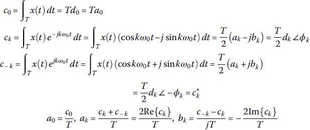
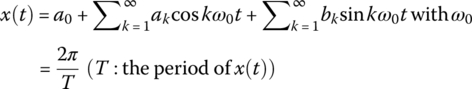
A function x(t) of t is said to be periodic with period T if x(t) = x(t + T) ∀ t, where T[s] and ω0 = 2π/T[rad/s] are referred to as the fundamental period and fundamental (angular) frequency, respectively, if T is the smallest positive real number to satisfy the equation for periodicity. According to the theory on Fourier series, any practical periodic function x(t) can be represented as a sum of (infinitely) many trigonometric (cosine/sine) functions or complex exponential functions, which is called the Fourier series representation. There are four forms of Fourier series representation as follows:
- <Trigonometric form>
where the Fourier coefficients a0, ak, and bk are
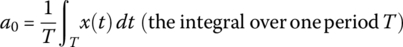
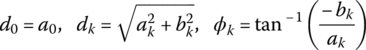
- <Magnitude‐and‐Phase form>
(1.5.2a)
where the Fourier coefficients are
- <Sine‐and‐Phase form>
where the Fourier coefficients are
- <Complex Exponential form>
(1.5.4a)
where the Fourier coefficients are
- Here, the kth frequency kω0 (k > 1) with fundamental frequency ω0 = 2π/T = 2πf0[rad/s] (T: period) is referred to as the kth harmonic. The above four forms of Fourier representation are equivalent and their Fourier coefficients are related with each other as follows:
- The plot of the Fourier coefficients (1.5.2b), (1.5.3b), or (1.5.4b) versus frequency kω0 is referred to as the spectrum, which can be used to describe the spectral contents of a signal, that is, depict what frequency components are contained in the signal and how they are distributed over the low‐/medium‐/high‐frequency range. The Fourier analysis performed by PSpice yields the Fourier coefficients (1.5.3b) and the corresponding spectra of chosen variables (see Example 1.5).
- <Effects of Vertical/Horizontal Translations of x(t) on the Fourier coefficients>
- Translating x(t) along the vertical axis by ±A (+: upward, −: downward) causes only the change of Fourier coefficient d0 = a0 for k = 0 (DC component or average value) by ±A. Translating x(t) along the horizontal (time) axis by ±t1 (+: rightward, −: leftward) causes only the change of phases (ϕk′s) by ∓kω0t1, not affecting the magnitudes dk or
 or |ck|.
(1.5.5)
or |ck|.
(1.5.5)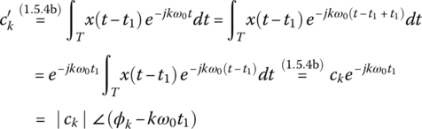
- Note that x(t − t1) is obtained by translating x(t) by t1 in the positive (rightward) direction for t1 > 0 and by −t1 in the negative (leftward) direction for t1 < 0 along the horizontal (time) axis.

1.5.1 Computation of Fourier Coefficients Using Symmetry
If a function x(t) has one of the following three symmetries, we can make use of it to reduce the computation for computing Fourier coefficients, as summarized in Table 1.1:
Table 1.1 Reduced computation of Fourier coefficients exploiting symmetries of x(t).
| Fourier coefficients | Symmetry of a periodic function with period T | ||
| Even symmetry: x(t) = x(−t) |
Odd symmetry: x(t) = − x(−t) |
Half‐wave symmetry: x(t) = − x(t + T/2) |
|
| a0(DC term) | 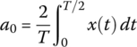 |
0 | 0 |
| ak(k = odd) |  |
0 |  |
| ak(k = even ) |  |
0 | 0 |
| bk(k = odd) | 0 |  |
 |
| bk(k = even ) | 0 |  |
0 |
Figure 1.12 Examples of rectangular and triangular waves.
- Even symmetry: x(t) = x(−t)
- Odd symmetry: x(t) = − x(−t)
- Half‐wave symmetry:

Note that an even (symmetric) function can become an odd (symmetric) one just by translation and vice versa as illustrated in Figure 1.12.
1.5.2 Circuit Analysis Using Fourier Series
In the previous section, we discussed how to represent a periodic function in Fourier series. In this section, we study how to analyze a linear circuit excited by a source whose value can be described as a periodic function of time, which is not necessarily a sinusoidal function. The procedure which we take to use Fourier series for analyzing circuits is as follows:
- Find the Fourier series representation of the periodic input function.
- Based on the fact that a (linear) system having transfer function G(s) responds to a sinusoidal input of frequency kω0 with the frequency response G(jkω0), apply the phasor method to find the individual responses to usually a few main terms, not necessarily every harmonic term, of the input represented in Fourier series.
- If necessary, add the DC and the fundamental frequency and harmonic components of the output based on the superposition principle to find the total response.
- (cf.) Note that the superposition principle holds only for linear systems.
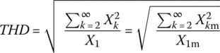
1.5.3 RMS Value and Distortion Factor of a Non‐Sinusoidal Periodic Signal
Let a non‐sinusoidal periodic signal have the magnitude‐and‐phase or sine‐and‐phase form of Fourier series representation as
Then its rms (root‐mean‐square) or effective value can be computed as
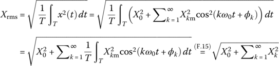
which is the square root of the sum of the squared DC (average) value (![]() ) and the squared rms values (
) and the squared rms values (![]() ) of every (fundamental and harmonic) frequency component contained in the signal. In this derivation, we have made use of the fact that the integral of a product of two sinusoids of different frequencies over their common period is zero:
) of every (fundamental and harmonic) frequency component contained in the signal. In this derivation, we have made use of the fact that the integral of a product of two sinusoids of different frequencies over their common period is zero:
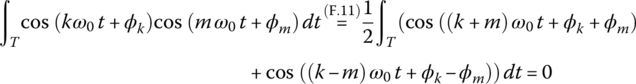
As a measure of how far a periodic signal is from its sinusoid of fundamental frequency, the THD (total harmonic distortion), also referred to as the distortion factor, is defined to be the ratio of the rms value of harmonic components to that of fundamental frequency component as follows:
Problems
- 1.1 Load Line on the v-i Characteristic Curve Instead of the i-v Characteristic Curve
- In Section 1.1, we write the equation for the load line to plot on the i-v characteristic curve as
(P1.1.1)
- How do you write the equation for the load line to plot on the v-i characteristic curve?
- What is the expression for the slope of the tangent line to the v-i characteristic curve of a diode at the operating point Q = (VQ, IQ)? Note that it is called the dynamic, small‐signal, AC, or incremental conductance.
- In Section 1.1, we write the equation for the load line to plot on the i-v characteristic curve as
- 1.2 Load Line Analysis of a Nonlinear Resistor Circuit
Consider the circuit of Figure P1.2(a), which contains a nonlinear resistor whose voltage-current characteristic curve is depicted in Figure P1.2(b).
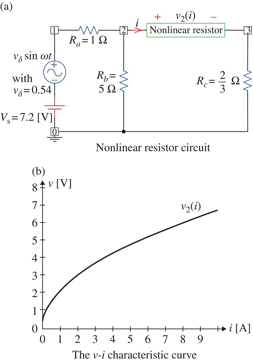
Figure P1.2 Graphic analysis of a nonlinear resistor circuit.
- Find the Thevenin equivalent of the circuit (with the nonlinear resistor open‐circuited) seen from nodes 2-3.
- Draw the load line on the characteristic curve of the nonlinear resistor to find the operating point (IQ, VQ).
- Noting that
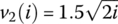 , find the static and dynamic resistances of the nonlinear resistor at the operating point Q by using Eqs. (1.1.10) and (1.1.7), respectively.
 - Using Eqs. (1.1.12) and (1.1.13), express the current through and the voltage across the nonlinear resistor in terms of the DC/AC components of the input voltage Vs and vδ.
- 1.3 A Nonlinear (First‐Order) RC Circuit Driven by a Sinusoidal Source
Consider the circuit of Figure P1.3(a) that consists of a nonlinear resistor, a linear resistor R = 500 kΩ, and a capacitor C = 14 [μF] and is driven by a DC voltage source of Vs = 6 [V] and an AC voltage source vδ sin t = 1.4 sin t [V]. The v-i relationship of the nonlinear resistor is i2(v) = v3[μA] and described by the characteristic curve in Figure P1.3(b). We can apply KCL at node 1 to write the following node equation:
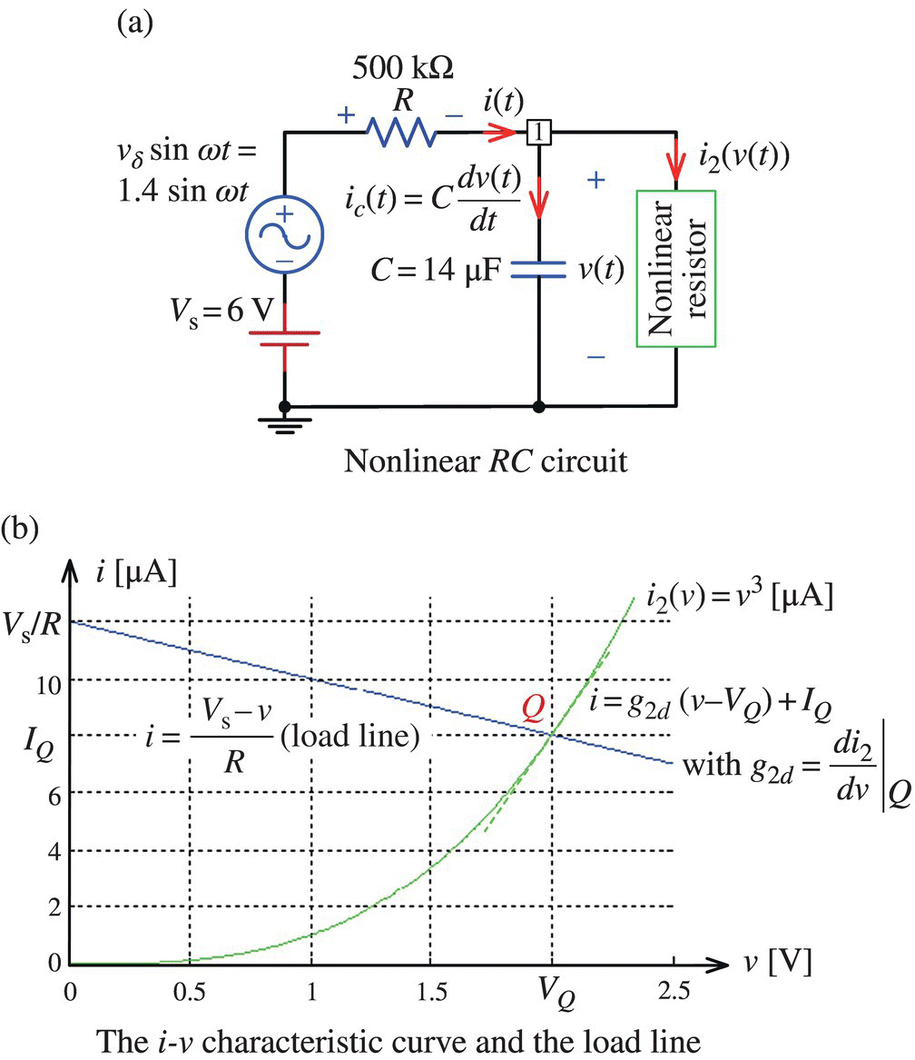
- Verify that the equation for the operating point Q in DC steady state is obtained by removing the AC source and the time derivative term and it can be solved as
(P1.3.2)
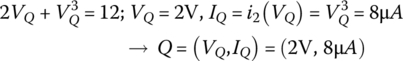
Also, draw the load line on the graph of Figure P1.3(b) to find the operating point Q from the intersection of the load line and the v–i characteristic curve of the nonlinear resistor.
- Use a MATLAB differential equation solver like ‘
ode45()’ to solve the nonlinear differential equation (P1.3.1) as done in Section 1.1.2. Also, try an iterative (dynamic) method to solve the nonlinear differential equation as coded in the following script “elec01p03b.m,” where the capacitor voltage or the voltage at node 1 is computed asPlot the two solutions together for comparison.
- Verify that the equation for the operating point Q in DC steady state is obtained by removing the AC source and the time derivative term and it can be solved as
- 1.4 (Thevenin) Equivalent Resistance of a Network Having Dependent Source
- Find the Thevenin equivalent of a CG amplifier in Figure P1.4 seen from d‐0(GND), which has a (dependent) current source of gmvgs = (vg − vs)/rgs where gm = 1/rgs and vg = 0.
Figure P1.4 To find the equivalent resistance seen from d-0 for Problem 1.4.
- 1.5 Lowpass Filtering of a Full‐Wave Rectified Cosine Wave
Figure P1.5(a) shows the PSpice schematic of a rectifier circuit in which a full‐wave rectified voltage vi(t) = |10 cos(2π60t)| is made smooth by an LCR low‐pass filter as can be observed from the input and output signals and their spectra in Figure 2.11(b) and (c). Note that in the Simulation Settings dialog box, the PSpice simulation parameters for Time Domain (Transient) Analysis are set as

Note also that in the Transient Output File Options dialog box (opened by clicking on Output File Options button in the Simulation Settings dialog box), the parameters for FFT analysis are set as in the following:
- Center (fundamental) frequency: 60 Hz
- Number of harmonics: 5
- Output variables: V(L:2) V(L:1)
Figure P1.5(b) shows the FFT analysis results for the input and output voltage waveforms of the LRC filter as listed in the PSpice simulation output file (opened by selecting PSpice>View_Output_File from the top menu bar of the schematic window).
- Noting that the transfer function and frequency response of the LRC filter are
(P1.5.1)
 (P1.5.2)
Figure P1.5 PSpice simulation of a rectifier for Problem 1.5 (“elec01p05.opj”).
and the Fourier series representation of the full‐wave rectified cosine input is
(P1.5.3)
verify that the first two major frequency components of the output can be expressed as
(P1.5.4)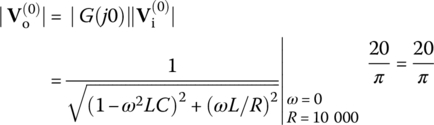 (P1.5.5)
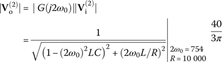
Write the condition for the relative magnitude of the major harmonic to the DC component to be less than rmax. Run the MATLAB script “elec02f12.m” (Section 2.2.6) together with MATLAB function ‘
elec02f12_f()’ to plot the region of (C, L) satisfying the condition as shown in Figure 2.12. Is the point (C = 1 μF, L = 50 H) in the 5%‐admissible region? - Modify the MATLAB script “elec01e06.m” (for Example 1.6) so that it can use the MATLAB function ‘
Fourier_analysis()’ to perform the spectral analysis of the input and output voltage waveforms for the full‐wave rectifier in Figure P1.5a and run it. Fill up Table P1.5 with the magnitudes of each frequency component obtained from the MATLAB analysis and PSpice simulation (up to four significant digits) for comparison. Is the relative magnitude of the major harmonic to the DC component less than 5%?
Table P1.5 Fourier analysis results obtained using MATLAB and PSpice.
Components PSpice MATLAB Input vi(t) DC component (k = 0) 5.091 Fundamental (ω0) 1.275 × 10 −30 Second harmonic (2ω0) Output vo(t) DC component (k = 0) Fundamental (ω0) 2.089 × 10 −20 Second harmonic (2ω0)