
CHAPTER 5
![]()
Diodes, Rectifiers, and Associated Circuits
Diodes are used almost everywhere for converting alternating current (AC) to direct current (DC), signal detection, switching or diverting signals, or even controlling the gain of signals. For example, in every AC adapter that generates a DC power supply, diodes are used whether the AC adapter is a conventional iron-core linear adapter or a highly efficient switching-power-supply circuit. In this chapter, we will explore the turn-on voltage characteristics of various types of diodes and some applications of diodes in electronic circuits.
Diodes and rectifiers are devices that conduct electricity in one way, or have polarity. Generally, rectifiers are relegated to applications that provide power or large signals, while diodes are often referred to as small-signal devices. Sometimes a device may be called a diode-rectifier, meaning that the diode can handle large currents or signals. Either way for this book, a diode is a device that handles both small and large signals, and a rectifier normally will just be used for large signals, such as a power-supply rectifier. In addition, zener diodes that are generally used for defining reference voltages will be briefly covered.
Characteristics of Diodes and Rectifiers
An ideal diode is a device that conducts with zero resistance in one direction and provides an open circuit in the other direction. For instance, if CR1 is an ideal diode instead of a 1N4002 or 1N4007 device and its anode is connected to a positive voltage, as shown in Figure 5-1, we would expect the voltage across resistor R1 to be 9 volts for the forward-bias mode and 0 volts for the reverse-bias mode when the battery’s negative terminal is connected to the anode.
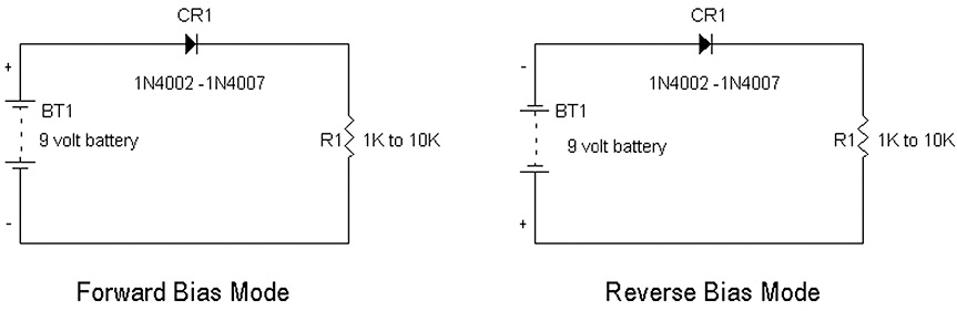
FIGURE 5-1 Forward- and reverse-bias connections of a diode.
However, with any manufactured diode, there is always a voltage loss across the anode to cathode when the diode is conducting (e.g., in the forward-bias mode). This forward voltage loss is sometimes called the forward voltage drop VF. The forward voltage drop depends on the type of material in the diode, such as silicon, germanium, or silicon with aluminum (a Schottky diode). To investigate the forward voltage drop of a diode, we can forward bias a power rectifier such as the 1N4002 and compare the voltage drop for various currents to a small-signal diode such as a 1N914 or 1N4148 (Figure 5-2).
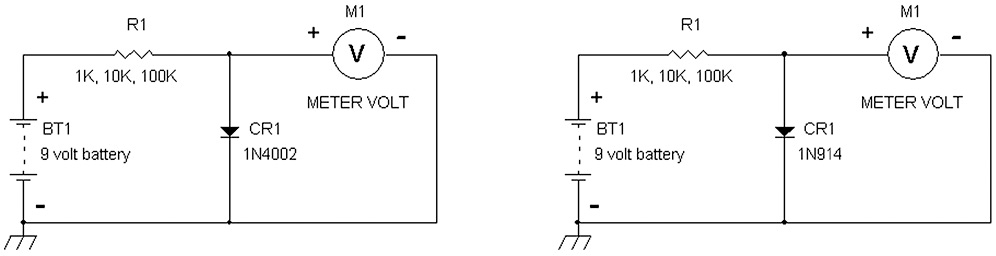
FIGURE 5-2 Experiments in measuring the forward voltage drop across the anodes and cathodes of a rectifier and a diode.
Parts List
• 9 volt battery and connector
• 1 kΩ, 10 kΩ, and 100 kΩ ohm resistors, ¼ watt, 5%
• 1N914 or 1N4148 diode or any silicon small-signal diode
• 1N4002 to 1N4007 rectifier or any silicon power rectifier
• Digital volt-ohmmeter (VOM)
For the experiment, the following results are shown in Table 5-1. Note that the reader may have slightly different results.
TABLE 5-1 Measured Forward Voltages of Diodes
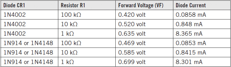
The diode current is calculated by finding the voltage across R1 (VBAT1 – VF), and using Ohm’s law, the diode current is
I = (VBAT1 – VF)/R1 Note: BT1 = VBAT1 = 9 volts
Small-signal diodes have appreciable internal resistances, while power diodes, by their nature to handle high currents inherently have low internal resistances. As shown in Table 5-1, at about 10 mA, VF, the forward-bias voltage, is higher with a 1N914 when compared to a 1N4002 power rectifier. Also note that for about every tenfold (10×) increase in current, the 1N4002 shows about a 100 mV to120 mV increase in voltage drop. Thus, for a hundredfold (10×) increase in diode current, the diode voltage increases somewhere in the range of 200 mV to 240 mV. From this observation, we see that a diode has a similar voltage-to-current relationship as an LED. For a tenfold (10×) increase in LED current the result is an increase in forward LED voltage (across the anode and cathode) in the range of 60 mV to 120 mV. Typical turn-on voltages are 0.2 volt for germanium diodes, 0.4 volt for Schottky (silicon-aluminum) diodes, and 0.6 volt for silicon diodes.
Converting AC to DC for Power Supplies
Probably since the beginning of electronics, one of the most common uses of diodes or rectifiers was to convert an AC voltage into a DC voltage. Vacuum-tube diodes served this purpose before the invention of solid-state diodes. The galena crystal diode, iron oxide or “rusty razor blade” diode, copper oxide, and selenium rectifier preceded the “modern” germanium and silicon diode.
There were early uses for converting AC signals to DC signals with diodes or rectifiers in the early part of the twentieth century. One was in the rectification of an amplitude-modulated (AM) signal for crystal and tube radios. A second use was just converting the AC power from the household power lines into a usable DC voltage supply to power tube amplifiers or radios.
Let’s first take a look at an AC signal. An AC signal holds positive and negative voltage (e.g., +1 volt and –1 volt) values. But just as a person cannot be in different places at the same time, a signal cannot be at two different values at the same time. A person can be at two different places at different times, and similarly, a signal or voltage can assume a different value at different times. Figure 5-3 shows a familiar sine-wave signal that oscillates between positive and negative peak values. Values above the horizontal axis are positive, and those below this axis are negative. An AC signal can be provided by an AC adapter that converts 110 volts or 220 volts from the wall socket to a lower AC voltage such as 10 volts AC.

FIGURE 5-3 Sine-wave signal with vertical axis showing amplitude and horizontal axis showing time.
Before delving into rectifier circuits, we should know the following about sine waves:
1. An AC voltage is usually rated in RMS (root-mean-squared) voltage. For this chapter, we will need to convert this voltage to its positive or negative peak value.
2. The positive and negative peak values of an AC signal are just 1.41 × RMS voltage. For example, if an AC adapter provides 10 volts AC (VAC), the positive peak value is +10 × 1.41 volts peak, which is +14.1 volts peak. Similarly, the negative peak value for this example is –10 × 1.41 volts peak, or –14.1 volts peak.
3. To convert back to RMS voltage when the peak voltage is known, the RMS volts = (peak voltage)/1.41. Using the preceding example, a 14.1 volt peak sine wave is = (14.1 volts/1.41) RMS = 10 volts RMS, which is what we would expect.
NOTE When you use a digital or analog VOM to measure AC voltage, the VOM is measuring only the RMS value.
Basically there are two types of common rectifier circuits, half wave and full wave. We shall examine the half-wave rectifier circuit first. See Figure 5-4.

FIGURE 5-4 Half-wave rectifier circuits to provide positive and negative DC voltages.
The left side of Figure 5-4 shows a rectifier circuit to provide a positive pulsating DC voltage, while on the right side a circuit is shown to provide a negative pulsating DC voltage. Both circuits as shown will generate average positive and negative DC voltages. Figure 5-5 shows rectification of the positive and negative cycles of a sine-wave voltage source with “ideal” diodes that have VF = 0.
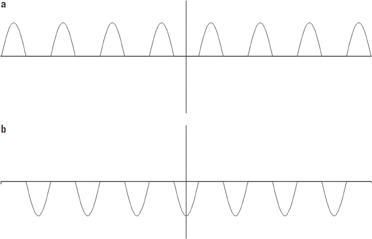
FIGURE 5-5 (a) Pulsating positive DC voltage, where the vertical axis is the amplitude and the horizontal axis denotes time. (b) Pulsating negative DC voltage, where the vertical axis is the amplitude and the horizontal axis denotes time.
If the peak positive voltage is +10 volts, the average voltage is +10 volts/π = +3.18 volts DC. One may ask why is it such a low number for the average voltage? After all, it’s about a third of the peak voltage. The reason is that unlike a +10-volt battery that gives out +10 volts DC all the time, the voltage shown in Figure 5-5a only peaks out at 10 volts for a short time, and at other times, the voltages are less than 10 volts. Also, the positive sine-wave cycles are “on” only half the time, while the other half of the time the waveform is flat-lined to 0 volt. Therefore, we know that the average voltage has to be less than 5 volts because half the time there is no voltage and the other half of the time the positive-cycle voltage of the sine wave is generally less than 10 volts. Figure 5-5b shows a negative half-wave rectified signal. Again, if the negative peak voltage is –10 volts, the average voltage is –10 volts/π = –3.18 volts.
NOTE In general, for a half-wave-rectified sine wave, the average voltage = peak voltage/π. Note that π ≈ 3.14.
Now let’s look at a full-wave rectifier bridge circuit. Before we apply an AC signal to it, we shall see that the full-wave rectifier circuit steers any positive or negative voltage to a positive voltage (Figure 5-6).

FIGURE 5-6 (a) Full-wave rectifier circuit with a 9 volt DC source attached to two of the inputs. (b) Full-wave rectifier circuit with the 9 volt battery reversed, with the same output voltage.
In Figure 5-6a, the output voltage into the load resistor R1 is supplied by the cathodes of CR1 and CR3 to provide a positive output terminal, and the anodes of CR2 and CR4 provide a negative output terminal. With the positive terminal of 9-volt battery BT1 connected to the cathode of CR2, we get a reverse-bias condition. So the only path for conduction from the positive terminal of BT1 is through the anode of CR1. Similarly, for the negative terminal of BT1 to flow current, it must be connected to the cathode of CR4. With the negative terminal of BT1 connected to the anode of CR3, we get a reverse-bias condition for CR3. Thus diodes CR2 and CR3 are turned off or essentially not connected. And therefore, we see that the only path of conduction is through diodes CR1 and CR4, which appropriately apply a voltage of positive and negative polarities across the top and bottom of R1. See the right side of Figure 5-6a.
In Figure 5-6b, we reverse the 9-volt battery’s connection to see the resulting output voltage. With the battery connections reversed, the negative terminal of BT1 is connected to the anode of CR1 and the cathode of CR2. The only path of conduction is via the cathode of CR2. Diode CR1 is running at reverse-bias mode and is therefore not conducting current. Now, looking at the positive terminal of BT1, we see that it is connected to the anode of CR3 and the cathode of CR4. Again, the only path of conduction is via the anode of CR3 to the positive terminal of the battery. Having the positive terminal tied to the cathode of CR4 results in a reverse-bias condition and no conduction of current. This essentially means that CR4 is an open circuit.
Therefore, CR1 and CR4 are open circuits with the only path of conduction being via CR2 and CR3. From the right side of Figure 5-6b, we see that again the voltage across R1 has the positive polarity on the top and the negative polarity on the bottom.
A full-wave bridge rectifier circuit then steers the input signal, whether positive or negative, to provide an output voltage of the same polarity. That’s pretty cool! This circuit is very useful not only for providing rectification of AC signals but also as a failsafe circuit so that if the battery or DC source is hooked up backwards at the input, the DC output voltage from the full-wave rectifier circuit always provides the (same) correct polarity.
Now let’s look at the full-wave rectifier circuit connected to an AC source. See Figure 5-7. The voltage across R1 is another pulsating DC waveform. Figure 5-8 illustrates the output of a full-wave rectifier circuit with “ideal” diodes where the forward bias voltage VF is zero.

FIGURE 5-7 An example of a full-wave rectifier with an AC input source.

FIGURE 5-8 Full-wave rectifier output signal.
For a full-wave signal as shown in Figure 5-8, how would we guess what the average voltage is if we know the peak voltage? We know from the half-wave rectifier signal that the answer is that:
Average voltage = (peak voltage)/π
But we also know that we have twice the amount of half-cycles in the full-wave signal than in the half-wave version. Figure 5-9 (and Figure 5-5a) shows the half-wave rectifier version.
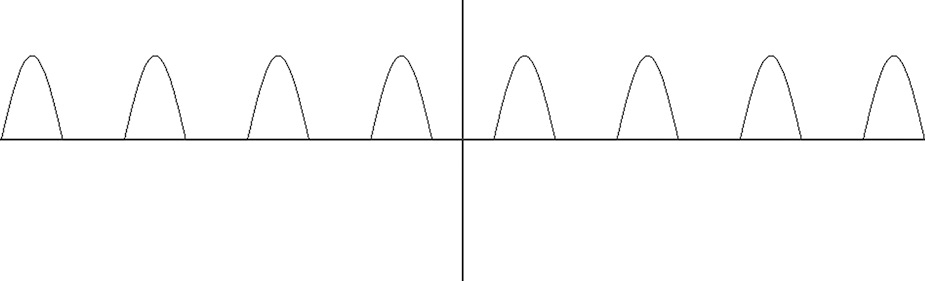
FIGURE 5-9 Half-wave rectifier output signal.
For a half-wave rectifier circuit we see that half the time there is a zero or flat-lined voltage. Thus, because there are twice as many (half) cycle pulses in the full-wave rectifier output signal compared with the half-wave version, we can deduce that the average voltage from a full-wave rectifier circuit is twice that of the half-wave circuit. Accordingly, then:
Average voltage from a full-wave rectifier circuit is 2 × (peak voltage/π)
For example, for a transformer supplying 10 volts peak, the average output voltage of a full-wave rectifier circuit using “ideal” diodes (VF = 0 volt) is 2 × (10 volts/π) = 6.36 volts DC.
For both circuits shown in Figures 5-4 and 5-7, the DC output is not usable for a power supply. The reason is that the DC voltage is fluctuating and at times goes to 0 volt. Although there is an average voltage from the waveforms in Figures 5-8 and 5-9, a circuit is required to provide an average voltage from these circuits. Such a circuit would be a low-pass filter. However, the simplest way to provide a more steady DC voltage is to simply add a peak-hold capacitor to the output of the diodes. See Figure 5-10.
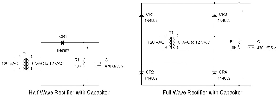
FIGURE 5-10 Half- and full-wave rectifier circuits with capacitors to convert the pulsating DC voltage into a more steady DC voltage.
In both circuits, the voltage output is about the peak voltage. The primary winding of the transformer takes in 120 volts AC, and the secondary winding delivers 6 volts AC to 12 volts AC into the rectifier circuits. At 6 volts AC, the peak voltage is 6 volts × 1.41 = 8.46 volts, which is approximately the voltage at C1 in both circuits.
Again, for a sine-wave voltage source, the peak voltage Vpeak = 1.41(VRMS). Note that VRMS is the rated AC voltage from the transformer. The actual DC output voltage is less. In the half-wave rectifier circuit, there is about a 0.6 volt loss due to the 1N4002 diode. Thus the output is (8.46 – 0.6) volts = +7.86 volts into C1.
In both rectifier circuits, the working voltage for C1 is 10 volts or greater. Usually it is best to pick a capacitor with at least a 50 percent margin over the peak voltage or, as a rule of thumb, just have the voltage rating of the capacitor at twice the peak voltage. For example, with 8.46 volts peak, choose a capacitor with a 16 volt or more rating.
For the full-wave circuit, the conduction path always goes through two diodes in series. See Figure 5-6 for the conduction paths. Thus in the right side circuit of Figure 5-10, there is a 2 × 0.6 volt loss, or 1.2 volts, which means from the full wave rectifier circuit, the output voltage with 6 VAC RMS, is 8.46 volts – 1.2 volts = +7.26 volts DC into C1.
Because the full-wave bridge rectifier circuit causes more loss at the output, why use it? The answer is that because the output pulses occur twice as often when compared with a half-wave circuit, the ripple voltage is half that from a full-wave circuit versus a half-wave circuit given the same load current and capacitor C1. Put in another way, for the same amount of ripple voltage, a full-wave rectifier circuit only requires half the capacitance value of the half-wave circuit.
There is a way to calculate what value C1 should be that depends on the current load. But, in general, for load currents up to about 0.5 amp, C1 should be on the order of 470 μF to 2,200 μF. For larger load currents of about 1 amp or more, I would recommend C1 at 4,700 μF to 10,000 μF.
DC Restoration Circuits and Voltage Multipliers
A DC restoration circuit “clamps” the positive or negative peak to a specific voltage such as 0 volt. In this section, we will explore the DC restoration circuit that clamps or repositions an incoming sine wave such that the negative peak is set to 0 volt or near 0 volt (e.g., –0.6 volt). See Figure 5-11. What makes the DC restoration circuit amazing is that the negative peak of the waveform is set to 0 volt regardless of the amplitude of the sine wave.
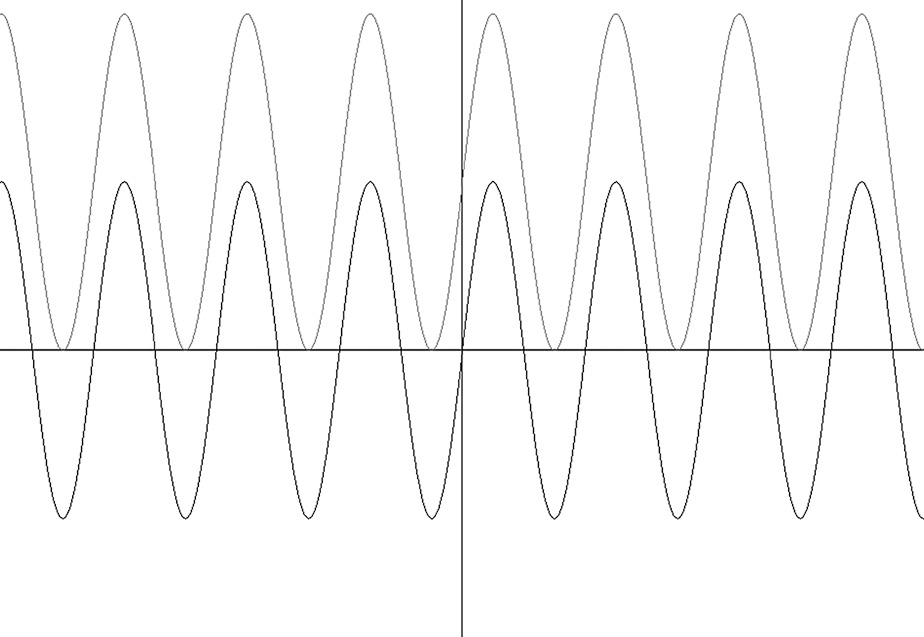
FIGURE 5-11 The bottom waveform is the input signal, and the top waveform is from the output of a DC restoration circuit.
A DC restoration circuit can be used to step up the DC voltage further by multiplication. Notice the AC peak-to-peak amplitudes of both waveforms are the same, but the absolute peak values are different between the top and bottom waveforms. In fact, the top waveform’s positive peak is twice the value of the bottom waveform’s positive peak. If each waveform were half-wave rectified and connected to a capacitor (see left side of Figure 5-10), the top waveform would provide twice the DC voltage as the bottom waveform and thus provide voltage multiplication.
Note that the input signal has a voltage swing of ±Vpeak, and the DC restoration circuit outputs a signal from 0 to +2Vpeak. For example, if the input signal is 10 volts AC RMS, the input signal has a swing from –14.1 volts to +14.1 volts. The DC restoration circuit then provides an output signal that swings from 0 volt to +28.2 volts. In essence, the DC restoration circuit has added a DC voltage of value +Vpeak to the AC signal source.
Now let’s look at a typical DC restoration circuit (Figure 5-12). The left side of Figure 5-12 shows a 10 volt AC signal from pins 5 and 8 of T1 connected to C1 and the anode of CR1. Therefore, the voltage from pins 8 and 5 of T1 swings from –14 volts to +14 volts and vice versa. CR1 and C1 form a half-wave rectifier and capacitor circuit, which allows C1 to be charged to 14 volts. That is, during the part of the AC signal when the voltage from pin 8 to pin 5 is +14 volts, CR1 conducts in the forward-bias mode and supplies +14 volts in the (+) and (–) terminals of C1. Once C1 is charged to 14 volts, we can consider it as a 14-volt battery, which is shown on the right portion of Figure 5-12.
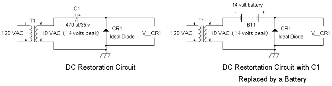
FIGURE 5-12 A DC restoration circuit (left). Replacing C1 with a battery for analysis purposes (right).
If we now look at the output voltage of the DC restoration circuit at V_CR1, note that the 14-volt battery BT1 on the right side of Figure 5-12 adds to the 10 volt AC signal from T1. Thus BT1 adds a level-shifting voltage equal to Vpeak of the 10 volt AC signal (14 volts). At this point, one can say the output at V_CR1 is a level-shifted AC signal.
To further illustrate how the DC restoration circuit works, see Figure 5-13. In Figure 5-13, BT2 represents the peak voltage from pins 5 and 8 of T1 at two different times. On the left side, the voltage referenced to ground is +14 volts, which is the peak voltage of T1 during its positive cycle. The voltage at V_CR1 for the diagram on the left is just the addition of two 14-volt batteries in series (BT1 and BT2) that results in a +28 volt output.
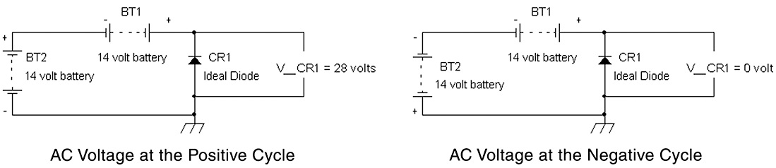
FIGURE 5-13 Using battery BT2 to denote the ±14 volt nature of the 10 volt AC signal for positive and negative cycles.
On the right side of Figure 5-13, the polarity of BT2 is reversed or alternated, which leads to two 14-volt batteries connected back to back with their (–) polarities. Thus the net voltage from BT1 and BT2 is 0 volt. Recall that in a two-cell flashlight, putting in the two batteries back to back results in no voltage going to the bulb. From Figure 5-13, we see that the range of voltages at the output V_CR1 is 0 to 28 volts, which is the AC waveform that has its negative peak clamped to 0 volt that results in a sine wave with a range of 0 to 28 volts.
To finalize making the voltage-doubler circuit, we simply add another diode and capacitor to peak hold the +28 volt portion of the level-shifted sine wave . See Figure 5-14. From Figure 5-14 the added second diode and capacitor CR2 and C2 allow capturing and storing of the +28 volts into C2, which results in Vout1 having +28 volts DC. Note that even though C2 is rated at 35 volts, it is preferable to have the working voltage increased to 50 volts or more. That is, it is better for C2 to be a 470 μF, 50 volt capacitor for an increased safety margin should there be a surge in the 110 volt AC line.
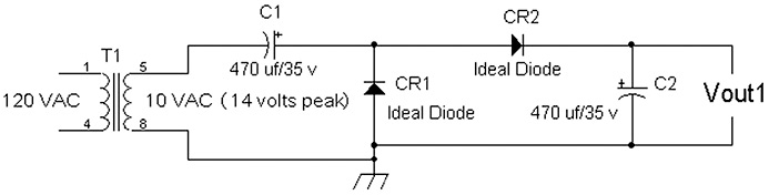
FIGURE 5-14 Voltage-doubler circuit completed by adding CR2 and C2.
The next question is, can we repeat the process of DC restoration and voltage doubling to make a 3× voltage multiplier? The answer is yes. See Figure 5-15.

FIGURE 5-15 A DC restoration to clamp the negative peak to +14 volts (above). A voltage-tripler circuit (below).
Suppose we want to generate even more voltage via a DC restoration circuit? We do not have to necessarily clamp the negative peak of the incoming sine wave to 0 volt. Instead, we can clamp the negative peak to a positive voltage. In Figure 5-15, the top circuit shows that the anode of CR1 is now connected to a 14-volt battery. This means that when the AC voltage across pins 8 to 5 swings to its peak voltage of +14 volts, the total voltage sent to C1 via CR1 is 14 volts plus 14 volts, or 28 volts. Note that although C1 is rated at 35 volts, using a 100 volt version is better. With 28 volts stored in C1, the incoming 10 volt AC voltage is level shifted by 28 volts instead of the 14 volts that is from the voltage-doubler circuit. Therefore, the signal at the cathode of CR1 of Figure 5-15 ranges from (+28 volts + 14 volts) to (+28 volts – 14 volts), which is 42 volts to 14 volts. By inserting a 14 volt source into the anode of CR1, the negative peak of the 10 volt AC signal is clamped to +14 volts. And because the 10 volt AC signal has a total of 28 volts peak to peak, the voltage range of the sine wave at CR1 is then +14 volts to +42 volts. If we harvest the +42 volt peak at CR1’s cathode via CR2 and store the voltage into C2, we get a +42 volt DC source at Vout3, which is triple the voltage from a simple half-wave or full-wave bridge circuit that gives out only +14 volts DC. The resulting circuit is shown in Figure 5-16.

FIGURE 5-16 A voltage-tripler circuit with CR3 and C3 providing the 14 volt source to BT1.
As shown in Figure 5-16, by using simple half-wave rectification via CR3 and using C3 as a peak-hold capacitor for the 14 volt peak voltage of the 10 volt AC source, a +14 volt source via C3 is then connected to the anode of CR1. Vout3 then provides about +42 volts DC. The reader is encouraged to build any of the circuits with 1N4004–1N4007 rectifiers and 100 volt electrolytic 470 μF capacitors in Figures 5-14 and 5-16. Just remember to observe the polarities of the diodes and capacitors and use safety glasses, just in case.
Diodes as Switches and Gain-Control Devices
A diode bridge circuit, as shown in Figure 5-17, may be used to gate or switch analog signals. Before the advent of CMOS (complementary metal oxide silicon) switches, the diode bridge circuit was commonly used (since the 1920s).
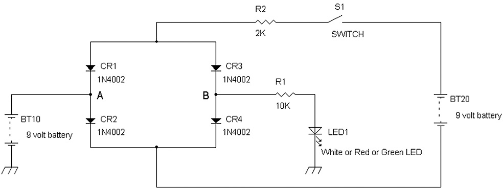
FIGURE 5-17 Diode bridge circuit for gating a signal through from points A to B.
Figure 5-17 shows a four-diode (CR1–CR4) switch circuit that is an open circuit when switch S1 is open because the diodes have no way to conduct via BT10. At first glance, CR2 may provide a conduction path from point A since the anode is connected to the (+) terminal of BT10. However, CR4 stops the current from flowing to point B since its cathode is tied to the cathode of CR2. When S1 is closed, current flows via BT20 and R2 to turn on all of the diodes, and conduction occurs from points A to B.
With the diodes in the forward-bias mode, each of them can be thought of as a low-power battery at 0.6 volt, as seen in Figure 5-18. Following the voltages from A to B via BT2 to BT4 or BT1 to BT3, we have voltages that are connected back to back. This back-to-back connection such as the voltages in series from BT2 and BT4 results in +0.6 volt (via BT2) and –0.6 volt (via BT4), which results in 0 volt between points A and B. Also see Figure 5-18. Note that a perfect wire with no resistance has no voltage across it from end to end when current flows through it [recall that V = IR, and if R = 0, then V = I (0 Ω) = 0 volt], so therefore the path from point A to point B is like a wire. And if A to B is like a wire, then there is connection from the 9-volt battery BT10 to light up LED1 via R1.

FIGURE 5-18 Bridge circuit with current flowing through the diodes, where the diodes’ turn-on voltages are represented as 0.6 volt sources.
Note that in Figure 5-17, CR1–CR4 may be replaced with small-signal diodes such as the 1N914/1N4148. Also, if the reader would like, CR1–CR4 may be replaced with LEDs, as seen in Figure 5-19. Also, the reader is encouraged to try different voltages for BT20, such as 1.5, 3, 4.5, and 6 volts, or different values of R1 (e.g., 2 kΩ, 4.7 kΩ, or 10 kΩ) to see if there is any effect on the brightness on LED1 in Figure 5-17 or LED5 in Figure 5-19. Figure 5-20 shows the completed circuit.

FIGURE 5-19 Electronic switching circuit using four LEDs instead of diodes.
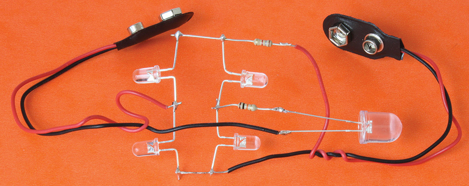
FIGURE 5-20 Three-dimensional (3D) prototype of LED switching circuit.
Parts List
• Two 9 volt batteries with connectors
• Four diodes (1N4002, 1N914, or equivalent) or, alternatively, four LEDs (any color)
• 2 kΩ resistor (or any resistor between 1,000 Ω and 3,300 Ω)
• 10 kΩ resistor (or any resistor between 10 kΩ and 22 kΩ)
• Switch, or just use a jumper lead to connect BT20 to R2
• White, red, or green (or yellow) LED
Experiment to Measure DC Resistance of Back-to-Back Batteries
Figure 5-21 shows that the resistance of two batteries connected back to back is less than 1 ohm. Normally, one does not measure the resistance of batteries with a VOM. But when they are of equal voltage and connected back to back, it is safe to measure the resistance, at least for a short while.
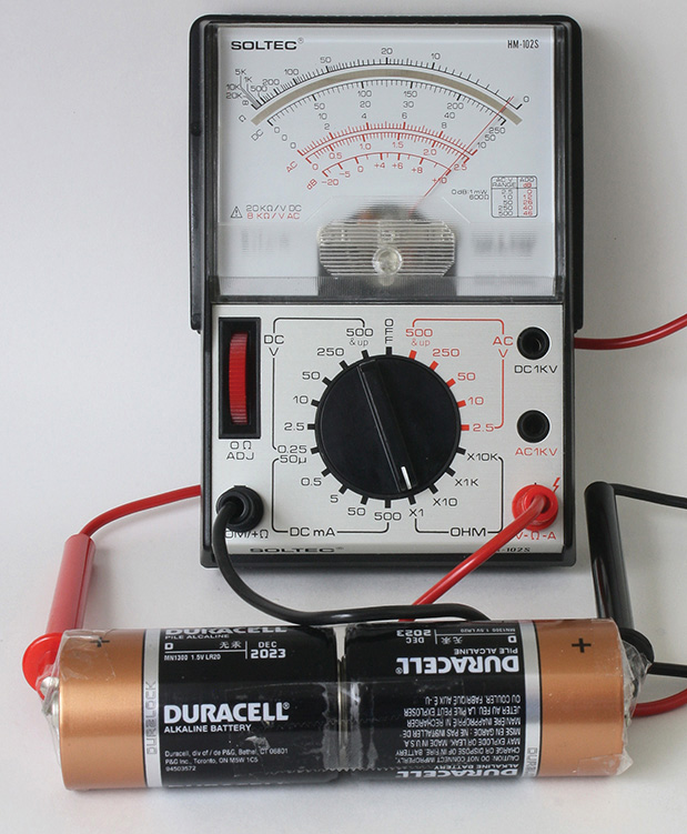
FIGURE 5-21 Top scale of VOM reads less than 1 Ω.
Parts List
• VOM (preferably an analog type, but a digital version will work)
• Two fresh batteries connected or taped back to back
Diodes as a Gain-Control Circuit
In radios or audio systems, electronic gain control is necessary to prevent overloading amplifiers down the chain. In the next experiment, we will look at how a diode can be used to vary the amplitude of an AC signal. Earlier we found out that both diodes and LEDs have a characteristic of increasing the diode or LED current 10 times when the voltages across them are increased by a small amount, such as 60 mV to 120 mV. What this said is that there is an exponential relationship between the input voltage and output current. This exponential relationship then offers a very useful characteristic in gain control in that the dynamic or AC resistance varies inversely in proportion to diode or LED current. For example, in a power diode such as 1N4002, the measured dynamic resistance was found to be 405 Ω at 0.10 mA, 47 Ω at 1 mA, and 4.8 Ω at 10 mA. We can show the dynamic resistance effect of a diode or LED by changing the forward-bias current (see Figures 5-22, 5-23, and 5-24). By setting R3 to 100 kΩ, 10 kΩ, 1 kΩ, or 470 Ω, the output signal is attenuated in various degrees.
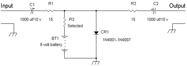
FIGURE 5-22 Diode attenuator circuit.
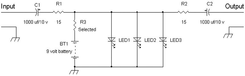
FIGURE 5-23 LED attenuator circuit.

FIGURE 5-24 3D prototype of the LED attenuator circuit.
Part List
• 9 volt battery and connector
• One 1 amp diode (e.g., 1N4002) for Figure 5-22 or three white LEDs for Figure 5-23
• 470 Ω, 1 kΩ, 10 kΩ, and 100 kΩ, ¼ watt resistors for selecting R3
• Two 15 Ω resistors
• Two 1,000 μF capacitors at 10 volts or more voltage rating
• Alligator clip leads
• CD player or radio with a headphone output
• One stereo or mono 3.5 mm cable
• Headphones or earphones
We will be listening to just one channel. Connect one end of the stereo 3.5 mm cable to a CD player. With alligator clip leads, connect the sleeve portion of the other end of the 3.5 mm cable to the ground connection of the circuit, as shown in Figure 5-22 or 5-23. Connect the tip of the 3.5 mm cable to another alligator clip lead, and connect the other end of the second clip lead to the input of either circuit. With another two alligator clip leads, connect the sleeve and tip of the headphone plug to the output and ground of the circuit being tested. Play a selection, and vary R3 to listen for an attenuation effect. Be sure to remove the headphones from your head before connecting or disconnecting any resistors to avoid hearing very loud clicks.
Radio-Frequency (RF) Mixing with a Diode
When we think of mixing, there are two types of mixers commonly used in electronics. One is the adding or summing mixer that combines two or more signals in a linear manner. When we talk of mixing in a linear manner, we mean that the two or more signals do not interact with each other to cause extra distortion signals. A good example of a linear mixer is an audio mixing board that is able to take multiple audio sources and combine them in an additive way.
The other type of mixer is generally used in radio-frequency (RF) to take two signals and provide an output signal whose frequency is the sum or difference of the frequencies from the two signals. For example, in an AM radio, the incoming RF signal has a frequency of 1.000 MHz. If the AM radio has an RF mixer, the mixer will receive the 1.000 MHz RF signal and a local oscillator signal at 1.455 MHz. The output of the mixer will then provide signals with frequencies of (1.455 MHz + 1.000 MHz) and (1.455 MHz – 1.000 MHz), which are the sum and difference frequencies of 2.455 kHz and 0.455 MHz. See Figure 5-25.
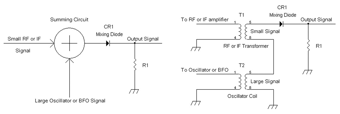
FIGURE 5-25 A top-level illustration of an RF mixer (left). Practical implementation (right).
One key to ensuring good RF mixing when using a diode as the mixing element is to provide a larger signal from the oscillator when compared with the incoming radio-frequency (RF) or intermediate-frequency (IF) signal. On the left side of Figure 5-25 we see a linear summing circuit in which the output of the summing circuit is fed to a diode that acts as a half-wave rectifier. Given the inherent turn-on voltages of diodes, the amplitude of the oscillator or beat-frequency oscillator (BFO) should exceed the turn-on voltage of the diode. For example, a silicon diode requires about 0.6 volt to start conducting current. Therefore, the oscillator should have an amplitude level greater than 1 volt peak.
The right side of Figure 5-25 shows the summing circuit as the series connection of two secondary windings for transformers T1 and T2. After summing the incoming RF (or IF) signal and the large-signal oscillator signal, half-wave rectification is applied at the output of the summing circuit, which results in output signals from the cathode of the diode CR1 with sum and difference frequencies of the RF signal’s frequency and the oscillator signal’s frequency.
NOTE A beat-frequency oscillator (BFO) is used for the detection of suppressed carrier signals such as (amateur radio) single-sideband (or double-sideband suppressed-carrier) signals. There will be more discussion of radio circuits and signals in Chapter 10.
We will wrap up the subject of diodes in the next three sections. These include logic circuits with diodes, variable-capacitance circuits using varactor diodes, and voltage regulators using zener diodes. Their uses will become more evident in later chapters when more advanced circuits are introduced.
Logic Circuits Using Diodes
A logic OR circuit consists of two or more inputs that have either a logic high or a logic low level. If any of the inputs are logic high, the output of the OR circuit will be logic high. In order for the output of the OR circuit to be logic low, all inputs must be at a logic low level. In essence, it takes a unanimous agreement for all inputs to a low logic level to create a logic low level at the output of the OR gate. However, any input may receive a veto, such as a single vote to go high to set the OR circuit’s output high (see Figure 5-26). For extra inputs, InputN is denoted, and CRN’s cathode is connected to OUTPUT1’.
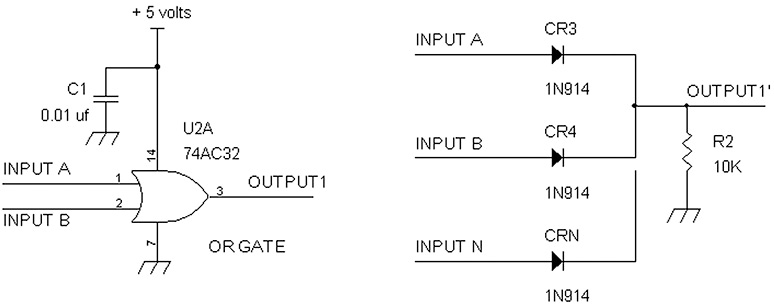
FIGURE 5-26 OR gate on the left and diode equivalent on the right.
For the AND circuit, we have a somewhat opposite effect. The output provides a logic high level when all its inputs are logic high. Therefore, it takes unanimous agreement to have all inputs set to the high logic level in order to provide a high logic level at the output of the AND circuit. But all it takes is a single low logic level at one of the inputs to veto the output of the AND circuit and provide a logic low output (see Figure 5-27). For extra inputs, CRN is denoted, and its anode is connected to OUTPUT2’.
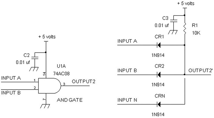
FIGURE 5-27 AND gate on the left and diode equivalent on the right.
Variable-Capacitance Diodes
Traditional variable capacitors have required a mechanical adjustment to vary the capacitance. Usually, a shaft is turned to rotate the plates of the variable capacitor (see Figure 2-46, lower right-hand corner). A variable-capacitance diode (varactor or varicap diode) takes the place of a mechanical variable capacitor and has the advantage of varying the diode capacitance electronically via a control signal, which allows faster speeds. Uses for the varactor include tunable RF amplifiers and oscillator circuits that are used in radios. The varactor diode can be used in an FM (frequency-modulation) transmitter to instantaneously change the FM carrier frequency by impressing an audio signal into the varactor. Figure 5-28 shows a low-power FM oscillator using a varactor diode (MV209) to modulate the FM carrier.

FIGURE 5-28 An FM oscillator circuit.
Note that the identification of the anode and cathode of Varactor1 (MV209), which comes in a two-lead TO92 plastic case, is as follows: when viewing the flat side in front with the two leads protruding down, the anode lead is on the left, and the cathode lead is on the right. The varactor diode works in reverse-bias mode, and the capacitance is maximum at about 0 volt between the cathode and the anode, and it has decreasing capacitance as the positive reverse-bias voltage is increased at the cathode. For example, with its anode grounded, the cathode of the varactor is biased via a large-value resistor of at least 100 kΩ (R4) to a positive voltage (via R5 and R6). The higher the positive voltage, the smaller is the capacitance delivered across the cathode and anode of the varactor diode. This advanced-level circuit can be built by the reader, but care must be taken, and the leads of all components around Q1 must be as short as possible. The oscillator’s frequency works within an FM broadcast band. The audio input signal may be taken from the output of a CD player or transistor radio via the headphone output. Tune an FM radio close to coil L1, and listen for the audio from the CD player or transistor radio.
NOTE Other types of diodes can be used as a varactor, such as a power diode (e.g., 1N5401) or a 12 volt zener diode.
Zener Diodes for Voltage Regulation
Another diode that is reverse biased is the zener diode, where the cathode is fed to a positive source and the anode is connected to a negative source. We do not hook up voltage sources (e.g., a battery or power supply) directly to a zener diode because that will cause overheating and destruction. Instead, the zener diode usually is driven with a current-limiting resistor or a current source. With a limited current flowing into the zener diode, the reverse biasing causes the diode to break down in a nondestructive manner. The breakdown voltage due to the reverse biasing is called the zener voltage.
We generally hook up via a resistor to the zener diode with a higher voltage than the zener voltage. For example, suppose that we have a raw 15 volt DC voltage that includes 60 Hz ripple and want to provide a clean 5 volt DC voltage without the ripple? One way is to connect a series resistor to a 5.1 volt zener diode’s cathode with its anode grounded and take the final voltage from the cathode of the zener diode to provide a regulated 5.1 volt supply that is free of 60 Hz ripple. If the 110 volt AC line goes up or down by 10 percent, the raw 15 volt DC supply will vary by ±1.5 volts or have a range of 13.5 volts to 16.5 volts DC. However, the output voltage at the zener diode still will provide a steady or solid 5.1 volts DC.
Zener diodes have generally two important characteristics—zener voltage and power rating. For example, a 1 watt, 12 volt zener diode allows a maximum current of about 80 mA flowing into it. Recall, by Ohm’s law, that P = IV, which leads to I = P/V. For this example, V = 12 volts, and P = 1 watt; therefore, I = 1/12 amp, or one-twelfth of an amp = 83.3 mA.
For a rule of thumb, we generally limit the zener diode current to about 60 percent its maximum rating. In the preceding example, we would set the zener diode current to 0.6 × 83 mA ≈ 50 mA. Note that the zener diode current is also the maximum current available for providing the regulated voltage. If the load’s current drain exceeds the zener biasing current, the voltage across the zener diode will drop below the zener voltage and will become unregulated.
We now close out this chapter with a power supply for providing ±17 volts unregulated and also ±12 volts regulated at approximately 50 mA (Figures 5-29 and 5-30).
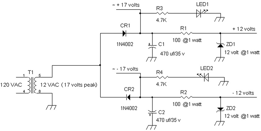
FIGURE 5-29 A ±12 volt regulated power supply.
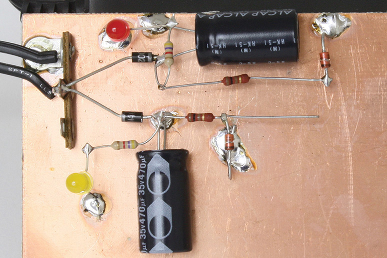
FIGURE 5-30 Prototype of ±12 volt regulated power supply.
Note that the zener diodes and 100 Ω resistors will get pretty warm. Any small component will get warm to at least mildly hot when dissipating at ¼ watt or more. So be careful when you touch the components.
From here on out in this book, the parts list will include the reference designations from the schematic. The reason is that with more complex circuits that include a variety of parts, having the reference designations (e.g., R1, C1, ZD1, LED1, etc.) and their values helps as a double-check against the schematic for accuracy.
Parts List
• 12 volt AC wall adapter transformer of at least 300 mA for T1
• Two IN4002 diodes for CR1 and CR2
• Two 470 μF or more capacitors at 35 volts or more for C1 and C2
• Two 4.7 kΩ, ¼ watt resistors for R3 and R4
• Two 100 Ω resistors at 1 watt or more for R1 and R2
• Two 12 volt zener diodes (e.g., 1N4742) at 1 watt or more for ZD1 and ZD2
• Two of any kind of LEDs for indicators LED1 and LED2
References
1. Motorola Small-Signal Transistors, FETs, and Diodes Device Data. Motorola, Inc., Schaumburg, IL, 1993.
2. Motorola TVS/Zener Device Data, 2nd. Ed. Motorola, Inc., Schaumburg, IL, 1994.
3. Motorola Zener Diode Manual. Motorola, Inc., Schaumburg, IL, 1980.