CHAPTER 6
![]()
Transistors, FETs, and Vacuum Tubes
Chapters 4 and 5 introduced light-emitting diodes (LEDs) and diodes, which we found can be used as switches or attenuators to control the strength of a signal. What neither LEDs nor diodes could do was to make the original signal larger. When a signal is switched, the signal is either on or off. And when a signal is already attenuated (i.e., reduced in strength) via a resistive divider circuit, further attenuation using LEDs or diodes as variable resistors does not provide for amplification. Therefore, in this chapter we will explore amplifying devices, which allow a signal to become larger in terms of either voltage or current or both.
Before delving into the concept of amplification, we will explore the concept of current sources. We can all relate to voltage sources such as batteries and power supplies, but we only had one introduction to current sources via Chapter 4 when photodiodes were presented as light to current-source devices. All active devices such as transistors, FETs (field effect transistors), and vacuum tubes can be characterized as some type of constant current source or variable current source that can output different amounts of electric current based on voltage across their input terminals.
We will also look briefly into operational amplifiers (op amps). In closing out this chapter, we will show briefly how an FET and a transistor can be used as a variable resistor.
Current Sources and Voltage-Controlled Current-Source Devices
The concept of a constant current source is that current flows into a resistor such that the resistor current is the same no matter what the resistance value is. For example, a constant current source that provides 1 mA (0.001 A) will cause 1 mA to flow into 100 Ω resistor R1 or 10,000 Ω resistor R2. That is, when a 100 Ω resistor is connected to a 1-mA source, the voltage across the resistor is (0.001 A × 100 Ω =) 0.100 volt. If the 10,000 Ω resistor is connected instead, the voltage across that resistor is (0.001 A × 10,000 Ω =) 10.000 volts. Figure 6-1 shows various circuits.

FIGURE 6-1 (From left to right) Current sources depicted by different load resistors R1 and R2 and a “practical” current source using a battery BT1.
In general, a current source needs a power supply to enable it for providing current. See the right-hand side of Figure 6-1. A simple way create a constant current source is to take a voltage source such as a battery and connect it in series with a resistor. See Figure 6-2. At first glance, this looks like a “lossy” voltage source, which, in a way, a current source is.
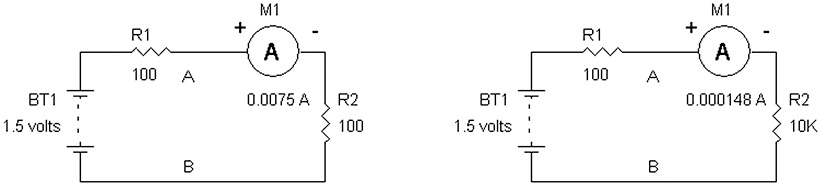
FIGURE 6-2 Two examples of lossy voltage sources with R1 = 100 Ω.
We know if we connect an external (load) resistor R2 across points A and B, the current into R2 will be BT1/(R1 + R2). Note: M1, the ammeter, has zero resistance. For example, if BT1 = 1.5 volts and R1 = 100 Ω, we know if a 100 Ω resistor is connected to points A and B, the current through R2 is 1.5 volts/(100 Ω + 100 Ω) = 0.0075 amp. If we change the value of R2 to 10 kΩ, the current is 1.5 volts/(100 Ω + 10 kΩ) = 0.000148 A. At this point, we do not have a constant current source because the current is not constant when R2 has a different value. What we want is if R2 is changed in value, the current through it stays essentially the same.
But what if we make the battery voltage BT1 really large, say, 100 volts, and the resistor R1 a large value such as 10 mega ohms (10M Ω)? See Figure 6-3.
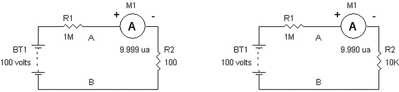
FIGURE 6-3 A lossy “high” voltage source that more closely resembles a constant current source.
Repeating the values of R2 = 100 Ω and 10 kΩ, we get R2 resistor currents of 0.009999 mA (9.999 μA) and 0.009990 mA (9.990 μA), respectively. Note that the two resistor currents are essentially the same. As you can see, such a circuit with a high-voltage supply and a large-value resistor approximates a constant current source generator. However, we can make current sources with transistors and FETs operating at lower voltages such as 3 volts to 15 volts.
Constant Current “Diodes” Using JFETs
One of the simplest ways to make a constant current source is to use a field-effect transistor (FET). As noted earlier, a FET has three terminals: a gate, a source, and a drain. Also known as a current source or current regulator diode, this circuit is nothing more than a JFET (junction field effect transistor) where the gate is tied to its source. Examples of current source diodes are the E500–E507. Before we look into this simple circuit, let’s take a look at JFETs. See Figure 6-4.
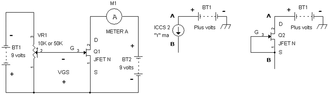
FIGURE 6-4 (From left to right) A FET biasing circuit, a constant current source ICCS2, and a JFET implementation of ICC2.
As seen on the left side in Figure 6-4, VR1 forms a voltage divider circuit with BT1 to apply a negative to zero voltage to gate G of Q1 with respect to Q1’s source S. In Figure 6-1, we showed a practical current source via ICCS2, which is shown again in the middle circuit of Figure 6-4, denoted by terminals A and B. By simply connecting the gate to the source of an N-channel JFET of Q2 (e.g., Siliconix FET, Part Numbers E105–E114 and E204), a constant current source circuit is provided, as seen on the far right in Figure 6-4. The battery voltage BT1 is large enough such that the voltage across the drain and source of Q2 is at least 1 volt.
JFETs in general are “depletion mode” FETs, which means that it takes a negative voltage from the gate to source for proper operation for an N-channel device. That is, for an N-channel FET, the gate and source terminals are in reverse bias. A zero volt potential across the gate and source of a depletion-mode N-channel FET is also allowable.
In a depletion-mode N-channel FET, zero volt across the gate and source denotes the maximum current for the FET, while a negative voltage across the gate and source that causes the FET’s drain current via M1 to go toward zero (e.g., a microamp) causes the FET to cut off current or to shut off. The “pinch-off” voltage in an FET is then the voltage across the gate and source such that no drain current flows. See the circuit on the left in Figure 6-4, where VR1 can be adjusted to a high negative voltage to cut off drain current from Q1. Typical pinch-off or cut-off voltages across the gate and source for N-channel JFETs vary from –1 volt to –10 volts.
When the gate to source voltage is reverse or zero bias, there is essentially no current flowing into the gate. But normally applying a positive voltage across the gate and source is not recommended because a forward bias condition occurs between the gate and source.
The circuit on the left side of Figure 6-5 shows the gate tied to the source to provide a fixed constant current to load resistor R1. By inserting a fixed or adjustable resistor in series with the source, the current can be varied (see Figure 6-5, right).
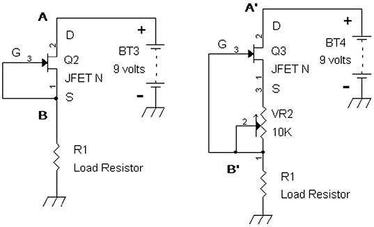
FIGURE 6-5 A constant current source (left). An adjustable current source (right).
Figure 6-5 shows an “improvement” over a constant current source by inserting a variable resistor VR1 (as shown) connected to Q3. The current source nodes are A’ and B’. The reader is encouraged to build either circuit in Figure 6-5, with the JFET being any N-channel JFET such as a 2N3819, J110, E108, etc. with R1 = 100 Ω and a 1 kΩ or 10 kΩ potentiometer for VR2 and measure the voltage at point B or B’ referenced to ground while varying the battery voltage of BT3 or BT4 from 3 volts to 9 volts. What should happen is the voltage at B or B’ will measure the same regardless of varying the battery voltage from 3 volts to 9 volts. The current is adjusted by varying VR2, which forms a voltage due to the current from the source terminal of Q3 flowing into VR2. The voltage is positive from the source S to the gate G of Q3. That is, connect the positive lead of a VOM to the source and the negative lead to the gate to read a positive voltage. Then connect the positive lead of the VOM to the gate and negative lead to the source of Q3, and you will read a negative voltage—which makes sense because the test probe leads of the VOM are reversed. This means the voltage from the gate G to the source S is negative, as required for depletion-mode FETs.
And in essence, VR2 is sometimes called a self-biasing resistor that does not require a negative voltage supply for biasing an N-channel depletion-mode FET (Q3 in Figure 6-5).
NOTE Some JFETs are symmetrical in terms of their drain and source connections. That is, swapping the drain and source leads is acceptable and generally provides the same result. In general, though, it is better to stick to connecting to the leads as labeled. Also note that the pin-out connections of various JFETs vary. So, accordingly, the reader should look at the labeling on the schematic for D, G, and S and not necessarily rely on the pin-out numbers 1, 2, and 3 on the drawing.
We will return to looking into FETs later, but for now, let’s take a look at bipolar transistors.
Bipolar Transistors as Current Sources
A bipolar transistor has three terminals: the emitter, base, and collector. When a transistor operates as a current source, a small amount of current flows into the base by applying a forward bias voltage across the base-emitter junction. The collector-to-base junction is generally reverse biased, while the collector provides the output current.
To operate an NPN transistor as current source, the voltage across the base to emitter is at its turn-on voltage of about 0.6 volt. Similarly, the emitter-to-base voltage of a PNP transistor has to have about 0.6 volt. NPN transistors are “opposite” in polarity to PNP transistors. And current sources can be made with both types; however, the current flow is different and opposite between NPN and PNP transistors. For now, we will investigate making current sources out of both.
In an FET, the source, gate, and drain terminals are analogous to the emitter, base, and collector terminals of a bipolar transistor. Unlike the FET, which operates without current flowing into the gate, the bipolar transistor requires base current. See Figure 6-6.

FIGURE 6-6 Biasing NPN and PNP transistors via R1 and R2 to provide NPN and PNP current sources.
NOTE If the circuits from Figures 6-6 and 6-7 are constructed, a copper-clad prototype board is recommended to avoid the transistors from oscillating. It was found that constructing these circuits on superstrip prototype boards resulted in unstable reading due to oscillations in the circuit. Thus, it is also highly recommended that a 1 μF capacitor with short leads is connected to the base-emitter and another 1 μF capacitor is connected to the collector-emitter terminals to each of the transistors. The capacitors will prevent the transistors from oscillating. Also, these circuits are suitable for testing transistors for current gain β.

FIGURE 6-7 Measuring changes in collector current for different values of collector load resistors for RL1.
There is a relationship between the base current and corresponding collector and emitter currents when the bipolar transistor is in an amplifying or current-source mode. This relationship is as follows: The collector current, IC = β (IB) and the emitter current, IE = (β + 1)IB, where β is the current gain, which varies from 10 to 1,000 depending on the transistor, and IB is the base current. For β or the current gain at 10 or greater, which is typical of most transistors, β ≈ (b + 1), which leads to IC = IE that says that for all practical purposes, the collector and emitter currents are equal. For example, if we take the worse case, where β = 10, then (b + 1) = 10 + 1 = 11. Thus, 10 is approximately 11 if we say that anything within 10 percent is roughly equal. Of course, if you are counting money, that’s another story when talking $10 and $11, and if you give someone $10 for an $11 payment, someone is going to be out by a buck!
Figure 6-6 shows a way of measuring collector current when driving the base with current via a base resistor of R1 = 470 kΩ. For example, on the left-side circuit in Figure 6-6, with a 2N3904 or 2N4124 NPN transistor for Q1, the following measurements were tabulated in Table 6-1 for R1 = 470 kΩ and 47 kΩ. Voltage measurements also were taken across the base-emitter junction of Q1. Base currents IB were calculated via IB = (BT1 – VBE)/R1 = (BT1 – VBE)/470 kΩ and IB = (BT1 – VBE)/R1 = (BT1 – VBE)/47 kΩ.
TABLE 6-1 Tabulation of Measurements for VB and IC with Calculated Values for IB and β

From Table 6-1, we see that the current gain β is not a true constant and that it changes value depending on the collector current. Also, if the reader measures the collector current with a 2N3904 or 2N4124 transistor, chances are that there will be different numbers from Table 6-1 because transistors in general have a wide range of current gain.
NOTE For measuring VBE with R1 = 470 kΩ, an inexpensive digital VOM has only a 1 MΩ input resistance, which would cause the VBE measurement to be in error by being slightly lower. Usually, one characteristic of an inexpensive digital VOM is that the resistance range only measures a maximum of 2 MΩ. For a more accurate reading, a midpriced digital VOM (around $30 or more) usually has a 10 MΩ input resistance, which is preferable for this experiment. The middle- to higher-performance digital VOMs usually have a resistance measurement range of at least 20 MΩ and sometimes to 2,000 MΩ. Also, most autoranging VOMs have 10 MΩ or more input resistance.
Concept of Measuring Collector Currents and Voltage Gain Due to Changes in Input Signals
In the next experiment, we replace the amp meter M1 with a load resistor RL1 and measure the voltage across RL1. See Figure 6-7.
When the load resistor RL1 is increased from 1 kΩ to 10 kΩ, we should expect to see more voltage across it and, more important, a greater change in voltage across RL1 as BT1’s voltage is changed when RL1 is increased in value. See Table 6-2.
TABLE 6-2 Measured Voltages Across RL1 via M3 and Calculated VCE from BT2 and M3
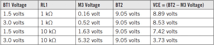
An extra column is added in Table 6-2, which calculated the collector to emitter voltage VCE based on BT2’s battery voltage minus the voltage drop across RL1 that is measured by M3. To measure VCE directly, place the positive lead of the VOM at the collector and the negative lead at the emitter of the transistor. Note that the direction of the changes in voltages for M3 is opposite for the changes in VCE. As the battery voltage in BT1 is increased from 1.5 volts to 3.0 volts, there is an increase in collector current, which is reflected in the voltage across RL1 = IC × RL1. However, the voltage at the collector of the transistor is VCE, and that is equivalent to (BT2 – IC × RL1) = VCE. Note: The M3 voltage = IC × RL1. So, as the voltage at the input via BT1 increases, the collector current increases, which also increases the voltage across RL1, but the voltage between the collector and emitter (VCE) decreases. When talking about AC signals, we say that the voltage measured at the collector (and measured not across RL1) referenced to the emitter is out of phase with respect to the input signal (i.e., BT1 changing from 1.5 volts to 3.0 volts). The collector current and voltage across RL1 as measured by M3 is in phase with the input signal since an increase in BT1 results in an increase in collector current and thus an increase in the voltage across RL1. That is, we can think of the voltage across RL1 as an equivalent battery voltage, V = IC × RL, where RL = RL1, as seen in Figure 6-8.
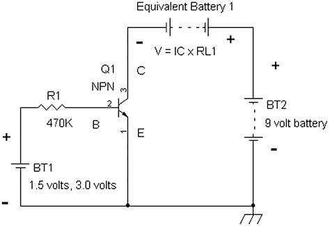
FIGURE 6-8 An equivalent battery voltage in place of the voltage across RL1.
As can be seen in Figure 6-8, the “Equivalent Battery 1” is connected back to back with the positive terminal of BT2. Thus, the resulting voltage at the collector of Q1 is (BT2 – V) where V = IC × RL. Therefore, the voltage at the collector of Q1 with respect to ground is VCE = (BT2 – IC × RL).
In terms of thinking about the changes in input battery voltages of BT1 from 1.5 volts to 3.0 volts, we can represent these two voltages as an AC signal that has a DC level-shifting voltage with the negative peak at 1.5 volts and the positive peak at 3.0 volts. Then we can also take a look at VCE as AC voltages with their DC level-shifting voltages. Figure 6-9 shows BT1 and VCE represented as sine waves for RL1 = 1 kΩ and 10 kΩ.

FIGURE 6-9 Three sine waves from bottom to top representing voltages of BT1, VCE @ RL1 = 10 kΩ and VCE @ RL1 = 1 kΩ. The vertical axis is the amplitude from 0 volt to 10 volts, and the horizontal axis is time.
From Figure 6-9, the bottom waveform is a sine wave from 1.5 volts to 3.0 volts, which represents the BT1 voltage range in Figure 6-7. BT1 can be thought of as the input voltage. The middle waveform, which is opposite in polarity or phase from the bottom waveform, represents the voltage range (7.42 volts to 3.73 volts) across the collector emitter (VCE) of Q1 in Figure 6-7 when BT1 changes from 1.5 volts to 3.0 volts for RL1 = 10 kΩ. Note that the VCE sine wave signal at the “output” via the collector of Q1 is larger than the “input” waveform, which is then amplification. Finally, the top waveform shows the VCE voltage swing of 8.89 volts to 8.52 volts when RL1 = 1 kΩ, which is smaller than the “input” waveform. Note that the “gain” of the amplifier is determined by the value of the load resistor RL1. Therefore, a transistor used as a variable current source provides amplification to the input signal, given a certain load resistor value.
Using LEDs as Reference Voltages
Now let’s construct a constant current source out of an NPN or PNP transistor using LEDs as voltage references. We can make use of the fact that red LEDs have a turn-on voltage (VF) around 1.8 volts and white LEDs operate at around 3.0 volts. Using LEDs as “constant” or well-defined voltage references replaces the 1.5 volt and 3.0 volt biasing batteries shown as BT1 in Figure 6-6. A reference voltage is a device that maintains its voltage output even if the supply voltage drops. In contrast, a simple voltage divider using two resistors connected to a power supply provides a divided output that is proportional to the supply voltage. That is, if the supply voltage drops by 50 percent, the output of the voltage divider circuit drops by 50 percent Figure 6-10 shows a voltage divider circuit on the left and a voltage reference circuit on the right.
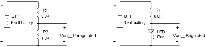
FIGURE 6-10 (From left to right) A voltage divider circuit and a voltage reference circuit using a LED.
The output voltage from a voltage divider in general is BT1 × [R2/(R1 + R2)]. For the circuit in Figure 6-10, Vout_Unregulated = 9 volts × [1.8 kΩ/(6.8 kΩ + 1.8 kΩ)] = 1.88 volts. If BT1 drops from 9 volts to 4.5 volts, Vout_Unregulated = 4.5 volts × [1.8 kΩ/(6.8 kΩ + 1.8 kΩ)] = 0.94 volt.
For the circuit on the right using LED1 as a voltage reference, Vout_Regulated is about 1.8 volts whether BT1 is 9 volts or 4.5 volts. The reader is encouraged to build both circuits and measure the output voltages with different battery voltages from 3 volts to 9 volts. Here is what was found from my experiment via Table 6-3.
TABLE 6-3 Measured Voltages for Voltage Divider and LED Voltage Reference Circuits with Different Battery Voltages
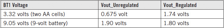
As can be seen in Table 6-3, the voltage output from the LED circuit is much more stable than the voltage divider circuit with varying battery or supply voltages.
Now let’s look at an example of using an LED and diodes for voltage references. See Figure 6-11.
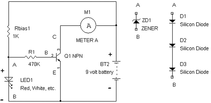
FIGURE 6-11 An NPN current source using a LED (left). Alternate voltage reference diodes (right).
Figure 6-11 shows LED1 to bias transistor Q1. Note that a red LED will provide about 1.8 volts across points A and B, whereas a white LED will give out about 3.0 volts. Alternatively, LED1 can be replaced with a zener diode or a series-connected string of diodes, each having a voltage drop of about 0.6 volt. Zener diodes come in voltages ranging from about 1.2 volts to over 100 volts. In this figure, one has to remember that the voltage reference device (LED, zener diode, or silicon diode) must have a voltage across A and B that is less than the battery voltage BT1. Put another way, the battery or supply voltage must be greater than the reference voltage; otherwise, the reference device will not be turned on. Note that the supply voltage should not be connected directly across the voltage reference diodes.
With the three diodes in series as shown (D1–D3) and biased via resistor Rbias1 (1 kΩ), the voltage across points (nodes) A and B will be about 1.8 volts, given that each diode has a forward bias voltage of about 0.6 volt. If we look at Figures 6-6 and 6-11, each transistor is driven with a base resistor to set up a collector current. This collector current is directly dependent on the current gain β of the transistor. However, the current gain of transistors even of the same part number or manufacturing lot will vary easily by 2:1 or even 3:1. For example, for the 2N3904, the range for β is 100 to 300. Thus, biasing a transistor with a single base resistor (e.g., R1 in Figure 6-11) is generally not done in circuit design unless the transistor has been selected for a range of current gains. This type of transistor current gain selection was and still is used today for certain inexpensive consumer products such as toys. For example, if Q1 in Figure 6-11 is replaced with various NPN transistors (e.g., 2N3904, 2N2222, and 2N5089) or even different 2N3904 or 2N4124 transistors, the current meter M1 will show a range of collector currents that can be twofold in difference.
By adding an emitter resistor and connecting a reference voltage at the base, a transistor circuit can be made to provide a known collector current essentially independent of the current gain as long as the transistor’s β is greater than 20. Figure 6-12 shows the addition of an emitter resistor to provide a collector current that is more stable and not as dependent on the current gain, β.
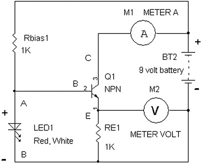
FIGURE 6-12 A stabilized collector current circuit using emitter resistor RE1.
In Figure 6-12, a second meter M2 is used for monitoring the voltage across emitter resistor RE1. If we recall, for transistor current gains β of at least 10, the collector current through ammeter M1 is essentially equal to the emitter current. The emitter current is just the voltage across RE1, which we can define as VRE1 divided by the resistance of RE1, which is 1 kΩ in this example. That is, Q1’s emitter current IE = VRE1/RE1.
For the next experiment, which can be made on a superstripe prototype board because we will be changing Q1 from a 2N3904 (β typically 100–300) to a 2N5089 (β typically 400–1,200), we will be comparing the circuits in Figures 6-11 and 6-12 in terms of sensitivity to current gain. Table 6-4 provides the measured results. If the reader tries this experiment, different collector currents may be measured, but in terms of sensitivity to β, the current gain, we will come to the same conclusion. That is, the circuit in Figure 6-12 will be superior in providing a more stable collector current IC with the two different transistors. See Table 6-4, where an LED1 is a red LED.
TABLE 6-4 Comparing Two Circuits for Collector Currents and Sensitivity to Current Gain
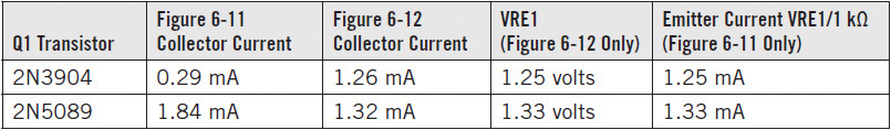
From Table 6-4, we see that indeed the circuit in Figure 6-12 is better in providing a stable collector current with transistors of different current gains. Note that VRE1 = LED1’s turn-on voltage minus VBE, Q1’s base-emitter turn-on voltage.
Given that the circuit in Figure 6-12 is stable in collector current “regardless” of the current gain of the transistor, as long as the current gain is greater than 10, and that the regulator diodes provide a “stable” voltage even when the power supply drops in voltage, we now have the makings of a constant current source that can be applied elsewhere. Table 6-5 shows the stability of the collector current when BT2 is changed in voltage for the circuit in Figure 6-12.
TABLE 6-5 Collector Current Stability with Variation in Voltage for BT2

Note that the circuit in Figure 6-11 also would yield a stable collector current with a variation in BT2’s voltage, which is characteristic of constant current sources. That is, the current output is relatively independent of the voltage across the current-source circuit.
Using a Constant Current Source to Provide Low Ripple at the Power Supply’s Output
In Chapter 5, we saw how to make a regulated power supply using 100 Ω resistors to bias 12 volt zener diodes. Although the regulation is good at 12 volts, this circuit, as seen in Figure 6-13, can be improved further.
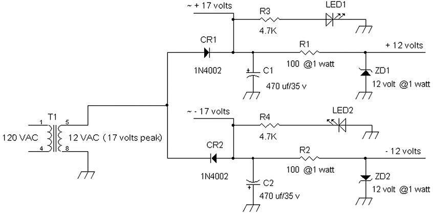
FIGURE 6-13 Regulated power supply using resistors R1 and R2 to bias zener diodes ZD1 and ZD2.
The voltage at the (+) side of C1, for example, has a ripple voltage at 60 Hz or 50 Hz depending on what part of the world T1 is plugged into. If we can supply ZD1 with a constant current source, the +12 volt output will have further lowered the ripple voltage. See Figure 6-14, where just the +12 volt supply is modified with a current source. Here the 100 Ω resistor R1 in Figure 6-13 is replaced by a constant current source using LED2 (red LED), Q2 (TIP32 or other power transistor), RE2 (22 Ω), and LED2 biasing resistor Rbias2 (3.3 kΩ). The collector current is determined by the voltage across RE2, which is the 1.8 volt LED2 voltage drop minus the 0.7 volt VEB turn-on voltage of Q2. Therefore, the voltage across RE2 is 1.8 volts – 0.7 volt = 1.1 volts. The current flowing through RE2 is then (1.1/22) amp ≈ 0.050 amp or 50 mA, which is also the collector current. To lower the collector current, a 24 Ω or 27 Ω resistor can be used for RE2 instead.
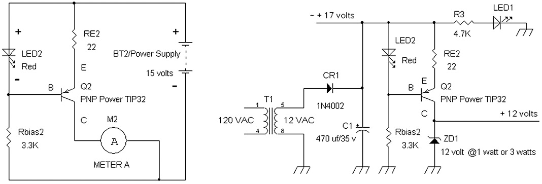
FIGURE 6-14 Left-side circuit shows a constant current source Q2, and right side shows this circuit integrated into a +12 volt power supply.
Note that a power transistor (TO-220 case) is used instead of a small transistor. That is, the raw supply’s voltage is 17 volts, and there is about 1 volt across RE2, so the voltage at the emitter of Q2 is 17 volts – 1 volt = 16 volts. Given that the zener diode ZD1 establishes about 12 volts at the collector of Q2, the voltage across the emitter and collector of Q2 is (the voltage at the emitter minus the voltage at the collector) = VEC = 16 volts – 12 volts = 4 volts.
With about 50 mA of collector current and about 4 volts across the emitter-collector junction, the power is IC × VEC (emitter-collector voltage) = 50 mA × 4 volts = 0.2 watt. Although a 2N3906 or 2N2907 may work, either would get really hot. It is safer, then, to use a 40 watt power transistor such as the TIP32 or, better yet, a 75 watt MJE2955.
In determining the current flow through Rbias2, we want to provide sufficient base current from transistor Q2 to generate about 40 mA of collector current. The voltage across Rbias2 is about 17 volts from the raw supply minus 1.8 volts from the LED2 voltage drop, which yields about 15 volts. Thus, the current flowing through Rbias2 is approximately (15 volts/3.3 kΩ) ≈ 4.5 mA. Because the current gain β of the TIP32 power transistor is at least 50 for a collector current of 50 mA, the required base current is 50 mA/50 = 1 mA. Thus, we have 4.5 mA available, which is more than enough for the base current requirement of 1 mA for providing 50 mA of regulated current.
If Rbias2 were made larger in value, such as 33 kΩ, the maximum base current would have been 0.45 mA, and with a β of 50, and the maximum collector current would have been 40 × 0.45 mA = 18 mA, which is short of the 40 mA we need. The bottom line is that if the collector current is not “regulating” to the desired current, decrease the base biasing resistor (Rbias2) to increase the current capability into the base of Q2. But just be aware of the power dissipated into Rbias2. The power into Rbias2 is about (15 volt)2/Rbias2. For a 3.3 kΩ, ¼ watt resistor, the power into it is (225/3,300) watt ≈ 0.068 watt, which is safely less than ¼ watt.
For a ±12 volt regulated power supply for 50 mA maximum current, Figure 6-15 provides a schematic of the circuit, and Figure 6-16 shows a prototype. Note that R1, R2, LED3, and LED4, which were the indicator lamps for the raw supply, can be removed. The reference LEDs, LED1 and LED2, can now serve for indicating voltage at the raw supplies (+17 volts and –17 volts).
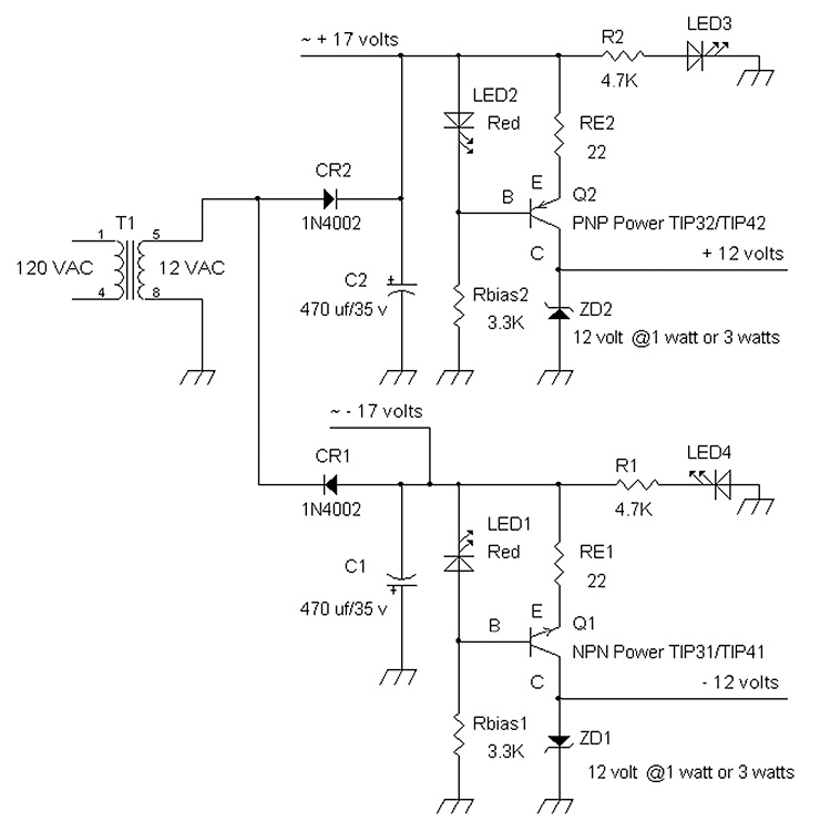
FIGURE 6-15 Regulated +12 and –12 volt power supply at approximately 50 mA.
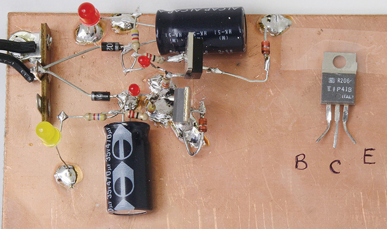
FIGURE 6-16 Voltage regulator circuit (left). Pin-outs B, C, and E to power transistors (right).
Parts List
• Two 470 μF, 35 volt electrolytic capacitors for C1 and C1
• Two 1N4002 or 1N4003–1N4007 diodes for CR1 and CR2
• Two red LEDs for LED1 and LED2
• Two any visible light LEDs for LED3 and LED4 (optional; may be omitted)
• Two 3.3 kΩ, ¼ watt resistors for Rbias1 and Rbias2
• Two 22 Ω, ¼ watt resistors for RE1 and RE2
• Two 4.7 kΩ, ¼ watt resistors for R1 and R2 (optional; may be omitted with LED3 and LED4)
• One NPN TO-220 power transistor such as a TIP31, TIP41, TIP3055, or MJE3055
• One PNP TO-220 power transistor such as a TIP32, TIP42, TIP2955, or MJE2955
• One AC adapter wall transformer with 120 VAC primary and 12 VAC secondary at 300 mA or more (for countries running on 220 volts AC, use an AC adapter with 220 VAC primary and 12 VAC secondary)
• Two 12 volt zener diodes at 1 watt (1N4742A) or preferably zener diodes at 3 watts (1N5913B or 3EZ12D5)
JFETs, MOSFETs, and Vacuum Tubes Used as Current Sources
JFETs, MOSFETs, and pentode vacuum tubes have current-source characteristics similar to those of bipolar transistors with at least one distinction. The gates of FETs and the grids of vacuum tubes are analogous to the base of the bipolar transistor, and the distinction between gates and grids compared with bases is that they do not draw current. In a bipolar transistor, base current is essential to producing an output collector current, whereas in an FET or a vacuum tube, only the voltage across the gate and source or a voltage across the grid and cathode is necessary to provide an output current. In this section, we will show similar experiments on biasing the devices. The main object is to show the reader some basic characteristics of these devices.
The reader at this point may be thinking that if all of these devices, that is, bipolar transistors, JFETs, MOSFETs, and tubes, can be used for constant current sources, is that the only use? The answer is no, and all these devices are also voltage-controlled variable current sources as well that lend themselves to providing for amplification.
For N and P channel biasing at the gates of JFETs, see Figure 6-17. It should be noted that JFETs normally are used for low-noise and RF (radio-frequency) applications. They are small-signal devices and are not available to handle higher power.
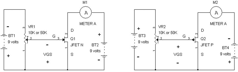
FIGURE 6-17 Reverse biasing of the gates of N- and P-channel JFET depletion-mode devices.
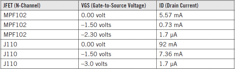
Examples of N-channel JFETs are the J110, 2SK152, MPF102, and 2N3819, and examples of P-channel JFETs are the 2N5460–2N5462 and J174– J177. As shown in Figure 6-17, the left-side circuit, a negative supply, BT1 is fed to VR1, which becomes an adjustable-voltage divider. The slider of VR1 is connected to the gate of Q1, applying an adjustable negative voltage with respect to the source S. That is, we are measuring the gate-to-source voltage VGS.
The output drain current for an N-channel JFET is measured by ammeter M1. Maximum drain current is specified when the gate-to-source voltage is zero. In terms of the cutoff voltage that causes a near-zero drain current (e.g., 3 nA = 0.003 μA), also known as the pinch-off voltage, this varies from –0.5 volt to –10.0 volts in most cases. Even within the same part number, the pinch-off voltage may vary 9:1. For example, an E107 N-channel JFET has a cutoff voltage from –0.5 volt to –4.5 volts for VGS. The question then arises with the wide range of pinch-off voltages how can we use them when manufacturing a product? One answer is to select the JFETs, and another is to provide an adjustment for the negative bias voltage. There is another solution as well, such as using a negative-feedback circuit to “servo” the drain current to a particular value by sensing the drain current or voltage and applying a voltage back to the gate of the FET.
On the right side of Figure 6-17 is the connection for a P-channel depletion-mode JFET; also note that everything is the same for the N-channel circuit except that the batteries are reversed in polarity. For just a feel of how JFETs behave, see Table 6-6.
TABLE 6-6 Applying VGS and Measuring Drain Current for Two N-Channel JFETs
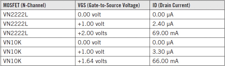
We now turn to MOSFETs, which are insulated-gate FETs. In a JFET, the gate-to-source terminals are reversed biased, and if the gate-to-source voltage is forward biased with +0.5 volt or more at the gate with respect to the source, there will be gate currents very much like forward biasing a diode. In MOSFETs, the gate is insulated, which means that any forward bias voltage does not incur gate current. Most MOSFETs are manufactured to be enhancement-mode devices. This means that the gate-to-source voltage is positive for N-channel devices. Despite the positive VGS, there is no current flowing into the gate. Enhancement-mode MOSFET devices come both in small-signal and large-signal power devices. For example, N-channel enhancement-mode MOSFETs are the VN2222L, VN10K, and IRF610, and examples of P-channel enhancement-mode devices are the VP0550, VP0610, and IRF9630.
However, it is possible to obtain depletion-mode N-channel MOSFETs such as the DN3545N3-G or LND150N3-G. Figure 6-18 shows the biasing of enhancement devices. Note that for the P-channel device, the polaritiy of the battery is reversed when compared with an N-channel transistor.

FIGURE 6-18 Biasing enhancement-mode MOSFETs for N- and P-channel devices.
For the next experiment, both medium- and high-power N-channel enhancement-mode devices will be measured for drain current as VGS is varied. It should be noted that enhancement-mode MOSFETs have turn-on voltages (aka threshold voltages) just like bipolar transistor. However, whereas the bipolar transistor has a well-known turn-on voltage of approximately 0.6 volt for silicon, enhancement-mode devices have turn-on voltages that vary quite a bit. For example, an N-channel enhancement device, such as the VN2222L, has a VGS turn-on voltage that varies from +0.6 volt to +2.5 volts. Tests of two N-channel MOSFETs were done using the circuit in Figure 6-18. If the VGS voltage is sufficiently high, greater than 2 volts, the MOSFET will act more like a switch. So VR3 had to be turned down to 0.00 volt first and slowly turned up. It is advisable not to exceed 100 mA of drain current or damage will be incurred in the MOSFETs or the ammeter. Table 6-7 provides some measurements.
TABLE 6-7 Measurements of Drain Current on N-Channel MOSFETs with Various Gate-to-Source Voltages
We now turn our attention to “hollow-state” devices, which are vacuum tubes. After all, why should solid-state devices such as bipolar transistors and FETs get all the attention? For this chapter, we will concentrate on the pentode, a five-element tube that has three grids, a plate or anode, and a cathode. There is also a heater or filament that needs to be heated up to allow electrons to flow from the cathode to the plate. As we have seen, the gate of an FET is analogous to the base of a bipolar transistor, and so is the control grid of a tube. The cathode of the tube is analogous to the emitter of a bipolar transistor and the source of an FET. Finally, the plate or anode of the tube corresponds to the collector and drain of a bipolar transistor and FET. So what are the other two grids for? The second grid is the screen grid that operates at about the plate power supply. The screen-grid voltage determines the gain of the pentode, but so does the control grid. The third grid, the suppressor grid, ensures that electrons that reach the plate do not bounce back to the cathode. The suppressor grid is usually connected to ground or to the cathode to provide a low potential such that any electrons bouncing off the plate get repelled back to the plate.
A pentode may be “converted” to a triode by connecting the screen grid to its plate. This results in a less than ideal current generator but generally provides for lower harmonic distortion and allows for lower plate voltages. For example, a 6AG5 or 6AU6 in pentode mode requires about 100 volts for operation, but if the screen grid is tied to the plate for triode mode, a plate voltage as low as 10 volts can be used.
Figure 6-19 shows a triode V1 with G1 as the control grid and a pentode V2 with G1 as the control grid, G2 as the screen grid, and G3 as the suppressor grid. Also, a pentode has its screen grid G2 connected to its plate to form a triode, and note that G3 is connected to its cathode, K. H1 and H2 are the heater or filament connections. Generally, the first single- or double-digit number for a tube denotes the filament voltage. For example, a 1R5 has a 1.4 volt filament voltage, whereas a 6AU6 and 35W4 have 6.3 volt and 35 volt filaments, respectively. It should be noted that most triodes (e.g., 6AT6, 6CG7, 12AX7, 12AU7, 12AT7, etc.) will work down to a plate voltage of about 10 volts.
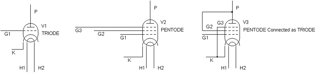
FIGURE 6-19 A triode, pentode, and pentode configured for triode mode.
In the 1950s, prior to the widespread use of transistors, specially made “space charge” vacuum tubes allowed pentodes, pentagrid converters, tetrodes, and triodes to operate “normally” at a plate voltage as low as 10 volts. Pentodes such as the 12DZ6, 12EA6, and 12AC6 were used commonly for car radio circuits requiring 12 volts DC. Thus, 12 volts supplied the 12 volt heater/filament and also ran the plate power supply. Figure 6-20 shows a bias experiment using one of these tubes. Note that although a 12DZ6 is shown in the figure, one can use a 12EA6 or 12AC6 for the experiment since the pin-outs are the same. Note that pin-out connections are not the same for all triodes or all pentodes. Be sure to go to the Web or check a tube manual to identify the plate, cathode, grid(s), and heater pin-out assignments for various tubes.

FIGURE 6-20 Measuring plate current as the grid-to-cathode voltage is varied.
NOTE The grid-to-cathode voltage ranges from 0 volt to a negative voltage, just like an N-channel JFET having a reverse-bias voltage across its gate and source. Also note that Figure 6-20 is very similar to the N-channel depletion-mode JFET measuring circuit in Figure 6-17 (left).
Tubes, like depletion-mode FETs, have cut-off voltages as well, and for a particular tube, the cut-off voltage is much better defined than for a JFET. Note that tubes are only N-type devices. There are no P-channel equivalents in vacuum tubes.
For the next experiment, we will include a space-charge low-plate-voltage tube (12EA6) and run some measurements. Also, a high-voltage pentode such as the 12BA6 will be connected in triode mode by connecting the plate’s pin 5 to the screen grid’s pin 6. Measurements will be made with just 12 volts for the plate voltage. See Table 6-8.
TABLE 6-8 Plate Current Measurements for Vacuum Tubes While the Grid-to-Cathode Voltage Is Varied

Brief Summary So Far
We have at this point seen that bipolar transistors, FETs, and even vacuum tubes can be used as constant current sources. On their own, constant current sources serve a limited function. Sure, they can be used for biasing zener diodes and other circuits, which you found out in this chapter (sneak peak: constant current sources are also used in the input and/or middle stages in integrated circuit amplifiers). A constant current source using any of these devices just means that we provide a known (constant) voltage across the base-emitter, gate-source, or grid-cathode of the bipolar transistor, FET, or vacuum tube to deliver a constant output current from the collector, drain, or plate.
In the experiments shown so far, we also varied the voltages at the input, which caused a change in output current. In a transistor, we can measure the change in input voltage across the base-emitter junction, or alternatively, we can determine the change in base current. Either way, a change in voltage or current at a bipolar transistor’s base terminal causes a change in collector current.
To provide amplification, we just can connect a load resistor to the collector of the transistor and determine the voltage swing across the load resistor or measure the collector voltage swing. In general, increasing the value of the load resistor increases the voltage gain. For example, see Figure 6-7 and Table 6-2. Similarly, in the experiments concerning FETs and vacuum tubes, we find that a change in voltage at the input to the gate-to-source junction of an FET or the grid-to-cathode connections of a vacuum tube will lead to a change in drain or plate current, respectively.
Just For Fun: A Low-Power Nightlight Using Transistor Amplifiers and LEDs
Here’s a circuit that turns on at night and shuts off in daylight or room light. The reader is encouraged to try out other photoreceiving devices than the LED used for sensing light. For example, a photodiode will have much more sensitivity to light (see Figure 6-21).
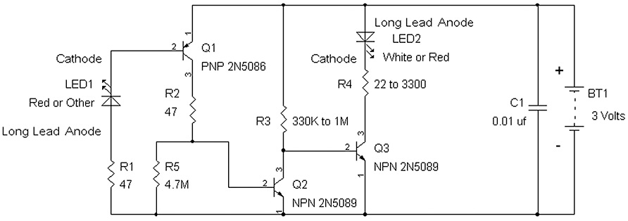
FIGURE 6-21 An automatic night light.
This circuit makes use of the current amplification characteristic of bipolar transistors. Generally, these transistors are also considered more to be voltage-to-current converters, but they are also current-to-current converters. So the photocurrent from LED1, which acts as a photodiode, is connected to the base of transistor Q1 to multiply the photocurrent by a current gain β1, and this multiplied current exits at its collector of Q1. The collector of Q1 sends the amplified current to Q2’s base, which amplifies again by a factor of β2 the current gain of the Q2. The collector current of Q2 then is the photocurrent from LED1 ×β1 × β2. When sufficient collector current is pulling from Q2, R3 will develop a voltage drop that causes the collector voltage at Q2 to approach 0 volt and shut off Q3 to turn off LED1. Thus, when there is sufficient light falling into LED1, LED2 shuts off. When LED1 receives very little light, there is insufficient photocurrent to be amplified, and the collector current of Q2 is too small to develop a sufficient voltage drop across R3. This allows current to flow from the power supply BT1 via R3 into the base of Q3 such that Q3 behaves as a current amplifier or a switch that turns on LED2.
Parts List
• Two 47 Ω resistors for R1 and R2
• One 330 kΩ to 1 MΩ resistor for R3 (try 330 kΩ first)
• One 22 Ω to 1 kΩ resistor for R4 to adjust brightness
• One 4.7 MΩ resistor for R5 for setting the threshold of the amount of light to turn off LED2 (start with 4.7 MΩ, but you can also try values from 1 MΩ to 3.9 MΩ)
• Two AA batteries with two-cell holder and connector for providing 3 volts DC
• One red LED or a photodiode for LED1
• One white LED (or other color) for LED2
• Two 2N5089 (or 2N5088) transistors for Q2 and Q3
• One 2N5086 (or 2N5087) transistor for Q1
• One 0.01 μF capacitor for C1 (any capacitor from 0.01 μF to 1 μF, film or ceramic, will do)
Note that the 47 Ω resistors for R1 and R2 are for protecting transistors Q1 and Q2 should there be excessive current due to too much photocurrent or should LED1 be inadvertently connected in reverse. Figure 6-22 shows the prototype.

FIGURE 6-22 LED night-light prototype circuit.
One can also use this circuit to test transistors. By substituting another PNP transistor for Q1 or an NPN for Q2, one can determine whether the transistor is working or not or has low current gain. In doing so, it is recommended that a photodiode (e.g., Osram SFH 229 from www.Mouser.com) should be used instead for LED1 so that sufficient current is generated by the light (R5 may have to be lowered to less than 1 MΩ). If an LED is used as the photodiode, you may have to place LED1 close by a lamp or shine a bright flashlight into it to turn off LED2. If a transistor is broken, it will either stay on all the time or stay off all the time regardless of how much light LED1 receives.
A Quick Look at Operational Amplifiers (Op Amps)
Integrated circuit (IC) operational amplifiers (op amps) are very common today in lieu of using discrete transistor amplifier designs. By nature, they have very large gains, typically greater than 10,000 (> 10,000). For example, if there is a DC voltage of 0.1 mV across the inputs of an op amp with a gain of 10,000, the output will be 1 volt. Let’s take a quick look at these devices for now. See Figure 6-23.
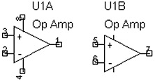
FIGURE 6-23 Example of a dual op amp.
As seen in Figure 6-23, an op amp has two terminals for the power supply, two terminals for the inputs labeled “+” and “–”, and an output terminal at the tip of the triangle. The two power-supply terminals for an op amp provide flexibility whether a plus and minus supply is used or either a single plus or minus supply is connected. In the single-power-supply example, one of the power-supply terminals is connected to common or ground. See Figure 6-24. When plus and minus supplies are connected, this allows the op amp to behave exactly like an ideal amplifier in terms of accepting AC signals and outputting amplified AC signal without having to use capacitors for coupling or level shifting.
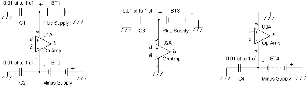
FIGURE 6-24 Op amps powered by plus and minus supplies, a single positive supply, and a single negative supply.
Op amps come with one or two op amps packaged in an 8 pin IC (integrated circuit), and four op amps in a 14-pin package. One should note that when a single supply is used, coupling capacitors are generally used to allow the transistors inside the op amp to have the proper DC biasing voltages.
When powering an op amp, the polarity of the plus supply terminal V+ and minus terminal V– must be obeyed accordingly. For example, most dual op amps have the V+ terminal as pin 8 and the V– terminal as pin 4. For proper operation, there must be a positive voltage measured from pin 8 to pin 4. That is, if one places the positive lead of a VOM on pin 8 and the negative lead on pin 4, a positive voltage should be read. An incorrect polarity into these terminals will generally result in permanent damage to the op amp. Also note that op amps require power-supply decoupling capacitors (C1–C4) on the order of at least 0.01 μF and preferably 0.1 μF or larger.
We now look at the input terminals of the op amp. See Figure 6-25. An op amp has a gain, which is called the DC open-loop gain. The DC open-loop gain can be thought of as the ratio of the output voltage to the input voltage across the (+) and (–) inputs. For example, if we put 1 microvolt (1 μV) of DC across the (+) and (–) inputs and get 10 volts out, the DC open-loop gain is then (10 volts)/(1 μV) = 10 million = open-loop gain for a DC signal.
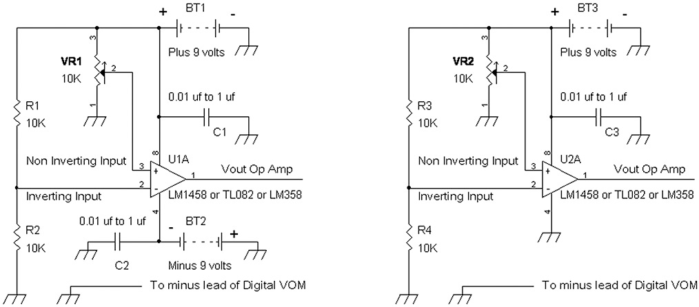
FIGURE 6-25 (Left to right) Op amps with high gain can be used as comparators when powered by dual and single power supplies.
Suppose that our power supply were limited to BT1 = V+ = +12 volts and BT2 = V– = –12 volts, and the op amp (on the left side of Figure 6-25) could output reliably from +11 volts to –11 volts, but we put 10 μV across the input. If the power supply were “unlimited” in voltage and the op amp could accept the unlimited power-supply voltage, the output would be 10 μV × 10 million = 100 volts. However, with the +12 volt and –12 volt power supplies, the output of the op amp will be limited to 11 volts for a 10 μV input. Depending on the polarity of the voltage at the input, the output will be positive or negative 11 volts. For example, if +10 μV is measured across the (+) and (–) input terminals, the output will be +11 volts, and if +10 μV is measured across the (–) (inverting input) and (+) (noninverting) input terminals, the output will be negative 11 volts. For a power supply of ±9 volts, Figure 6-25 (left side) shows that the voltage at the (–) or noninverting input terminal is one-half the supply voltage of 9 volts, or +4.5 volts. A variable voltage is applied to the noninverting input. If the noninverting input is below +4.5 volts, the output on the left side circuit will swing down to about –7.5 volts in practice. If the noninverting input voltage is above +4.5 volts, the output will swing to about +7.5 volts in practice. For the op amp on the right in Figure 6-25 with a single +9 volt supply, BT3, the output range is +7.5 volt to about +1.5 volts. One should try building these two circuits to get a feel for the output range of op amps. Why are these two circuits called comparators? They are comparing two voltages from VR1 or VR2 against the +4.5 volts via R1 and R2 or via R3 and R4. Any voltage from the variable resistors higher than +4.5 volts is a “logic” high state, and for any voltage below +4.5 volts, the output of the op amp swings to a low logic state.
Is it possible to try to set the input voltage very carefully to have a set output voltage such as 0 volt for the circuit on the left that has plus and minus supplies? The answer is no, not normally, unless some type of feedback mechanism is included. Any slight variation in power-supply voltage or any changes in resistance to R1, R2, or VR1 will cause the output to tip toward the plus or minus supply voltage.
Therefore, op amps normally use some type of feedback, where there is a DC path from the output to the inverting input terminal. Figure 6-26 shows a variable resistor VR1 connected from the output terminal to the inverting input. The noninverting input has a DC voltage of approximately 5 percent of +9 volts, or about +0.45 volt. By varying VR1, the output voltage will vary from about +0.45 volt to about +5 volts. If one measures the DC voltage at the noninverting and inverting input terminals, one will find almost the same voltage. Or put another way, if the voltage is measured across the noninverting and inverting input terminals at pin 3 and pin 2, the voltage will be close to 0 regardless of the setting on VR1. One can try this measurement with a digital VOM to confirm that indeed when an op amp has negative feedback as shown in Figure 6-26, putting the positive lead on pin 3 and the negative lead on pin 2 results in a VOM reading of nearly 0 volt.
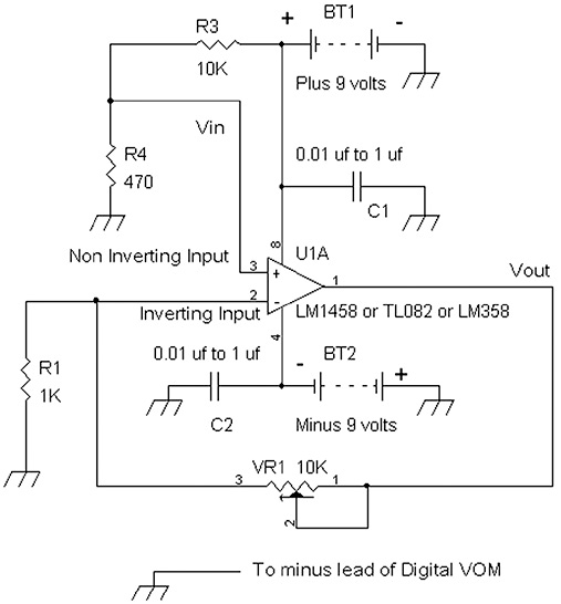
FIGURE 6-26 Negative-feedback configuration for an op amp.
The 0 volt across the noninverting and inverting inputs is sometimes called a virtual short circuit across the input. But, in reality, there is no short circuit here! The 0 volt condition is really a consequence of the open-loop gain being very high. Recall that for high-open loop gains, all it takes is on the order of a few millivolts or less at the input to cause the output to swing toward the power-supply voltages. Therefore, as long as the output of the op amp is less than its maximum output voltage, the input voltage, or, more appropriately, the voltage across the (+) and (–) inputs will be on the order of less than a few millivolts. For example, for an op amp with an open-loop gain of 3,000, a few millivolts across the (+) and (–) inputs will yield 3,000 × 3 mV = 9 volts at the output. For higher open-loop gains, the voltage across the (+) and (–) inputs will be smaller—hence coming to the “conclusion” that the (+) and (–) inputs approach 0 volt and thus become a “virtual” short circuit. (I suppose that the (+) and (–) inputs under a negative-feedback condition “play” a short circuit on TV, but in reality, the two inputs are not really a short circuit—a takeoff on the old joke about an actor saying that he or she is really not a doctor but only plays one on TV.)
We now turn to how to correctly use op amps with a single supply. By the way, all op amps advertised as single supply op amps will work with plus and minus supplies, and all op amps that generally are shown to work with plus and minus supplies will work on a single supply if biased correctly and if there is sufficient voltage (e.g., usually at least 6 volts) to power the op amp.
On the left-side circuit of Figure 6-27, the op amp is powered with a single positive power supply. This means that the output is limited to voltages greater than 0 volt. With an AC signal that has positive and negative voltages connected to the input, the output cannot generate a negative voltage because the V– power pin is connected to ground or 0 volt. Thus, we need to add a DC voltage to the AC signal such that we get a varying positive DC signal that is greater than 0 volt. See the circuit on the right in Figure 6-27.

FIGURE 6-27 Two op amp circuits connected to single supplies, but they require more work for proper operation.
In the circuit on the right in Figure 6-27, the input signal “Vin AC Signal” is connected to a coupling capacitor Cin, which allows R2 and R3 to level shift the AC signal to average at one-half the plus-supply voltage. This results in having +4.5 volts at the (+) input terminal, which is a good start to solving the problem. If VR1A is set to 0 ohms, the output is connected to the inverting input. By virtue of the fact that the voltage at the (–) input is the same or very close (within a few millivolts) to the (+) input, the output will then also be +4.5 volts because the (+) input terminal has +4.5 volts. Pretty cool, eh? The op amp servos the output voltage to the same voltage as the (+) input for VR1A = 0 Ω.
Now let’s see what happens if VR1A is set to1 kΩ. Because R1A is also 1 kΩ, the voltage at pin 2, the (–) input, is half the output signal at pin 1 because a divide by two voltage divider circuits consists of two equal-valued resistors. The (+) input is +4.5 volts, so the op amp will want to make the output 9 volts because VR1A = 1 kΩ and R1A = 1 kΩ will divide the 9 volts from the output in half to +4.5 volt. Unfortunately, a real op amp such as an LM1458 will deliver about +7.5 volts maximum at its output, the result is that the output has now “clipped” or saturated and is no longer working as an amplifier. Let’s take another example by setting VR1A to 9 kΩ. The voltage division formed by a 9 kΩ (VR1A) and a 1 kΩ resistor resulted in a division of voltage of 10. Because there is +4.5 volts at the (+) input terminal, in order to get +4.5 volts at the (–) input terminal, the output would have to be +45 volts, which is impossible given that BT2 is a 9 volt supply. That is, the maximum output voltage of the op amp is less than or equal to the power-supply voltage. It would be a great trick if we could get 45 volts out of an op amp powered with just 9 volts—but sorry, this will not work.
So how do we solve the problem? Ideally, we want the output to be sitting at about one-half the power-supply voltage so that its voltage swings are about equal going toward +9 volts and down toward 0 volt. It looks like an extra capacitor (C3) has come to the rescue to solve our problem (see Figure 6-28).
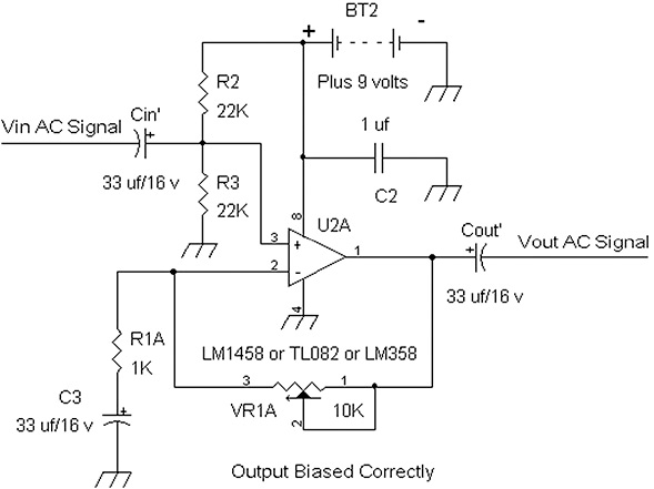
FIGURE 6-28 Single-supply op amp biased correctly.
In Figure 6-28, let’s take a look at our “new” DC voltage divider circuit VR1A, R1A, and C3. Instead of having the bottom lead of R1A going to ground, we put a “large” capacitor in series with it before connecting to ground via the negative terminal of C3. If we follow the DC voltage from VR1A to R1A, initially, C3 will act like a short circuit to ground, but because the DC voltage is being provided by pin 1, via VR1 and R1A, C3 is being charged up, and eventually, there will be no more current flowing into C3 after a warm-up period of less than a second. Note that it does not matter what value of resistance VR1A has, eventually, C3 will be charged up. If there is no DC current flowing into C3, there is also no DC current flowing through VR1A and R1A. Therefore, the DC voltage across VR1A is 0 volt because by Ohms law, V = IR, and because I = 0, V = 0R = 0. We can then see that for DC purposes, the DC voltage at pin 1 is the same DC voltage as at pin 2, the inverting input. But the voltage at pin 3 is +4.5 volts, and since the voltages at pins 3 and 2 are the “same,” the output, pin 1, has to be also +4.5 volts.
Another intuitive way to look at this is that for DC purposes, C3 is an open circuit, so take C3 out for finding out the DC voltage at the output. This leaves a voltage-divider circuit consisting of only VR1A because the bottom of R1A is now connected to an open circuit or to “nowhere.” A voltage divider consisting of just one resistor provides no voltage division at all, and all the voltage going into the resistor (VR1A to pin 1, the output terminal) also comes out with the same voltage at the other end (VR1A to pin 2, the (–) input). Therefore, we have the +4.5 volts at pin 3, the (+) input, to servo the output to +4.5 volts so that the (–) input is also +4.5 volts.
JFETs and Bipolar Transistor as Voltage-Controlled Resistors
Finally, we turn our attention to using FETs and bipolar transistors as voltage-controlled resistors. When used as part of a voltage-divider circuit, that is, the resistor that goes to ground but is a variable resistor, we get to use a control voltage to adjust the resistance of the bottom resistor of a voltage-divider circuit (see Figure 6-29).

FIGURE 6-29 JFET Q1 variable resistor and a bipolar transistor Q2 voltage-controlled resistor.
One of the differences that you will see with the voltage-controlled resistors in Figure 6-29 is that there is no DC biasing to drain and no collector for the FET Q1 and for the bipolar transistor Q2, respectively. It turns out that JFETs make very good voltage-controlled resistors. They are used in low-distortion Wein bridge sine wave oscillators to control gain of the oscillator’s system. For an N-channel device, a negative bias voltage is applied to the gate-to-source junction. The resistance is a function of the negative bias voltage. The more negative the gate-to-source voltage is, the higher is the resistance from the drain to source. Less negative bias provides a lower resistance from the drain to the source. The voltage divider is formed by R1 and the drain-to-source resistance of Q1 (e.g., MPF102, 2N3819, or J110).
A voltage-controlled resistor can be made from a bipolar transistor. The method is tricky and not obvious. The circuit you see on the right in Figure 6-29 is a practical circuit used in a Superscope CD-302A cassette tape recorder for its automatic level control amplifier. What is shown is just the variable-resistance portion of the amplifier, and it is not the complete automatic level control amplifier. A forward bias voltage from BT2 and VR2 turns on Q2 via diode D1. Applying a voltage to R6 causes the collector-to-emitter resistance to decrease. Thus, the collector-to-ground resistance changes and provides more attenuation. The initial value for VR2 is 10 kΩ, but a lower-resistance potentiometer may work better, such as 1 kΩ. Typically, the input AC signals levels are less than 1 volt peak to peak, and the outputs are followed with ×100 or more gain amplifier.
References
1. Power Products Data Book. Dallas, TX: Texas Instruments, 1985.
2. FET Data Book, Santa Clara, CA: Siliconix, Inc., July 1977.
3. Transistors Small Signal Field Effect Power. Santa Clara, CA: National Semiconductor, May 1974.
4. RCA Receiving Tube Manual RC-29. Harrison, NJ: RCA Corporation, 1973.