
CHAPTER 16
![]()
A Review and Analysis of What We Have Built So Far
Some circuits that were shown in previous chapters will be reviewed in this chapter with a more detailed analysis. We will start with frequency-response analysis of some of the amplifying circuits such as Wein oscillators and audio amplifiers. Also, we will look into how amplifying systems work. Most amplifiers include an input stage and an output stage. The characteristics of gain, frequency response, input and output resistances, and feedback will be analyzed. We will take a second look at Wein oscillators and radios with alternative circuit designs that generally lead to an improvement in performance. For example, in the Wein oscillator, it was found that larger-wattage bulbs caused the output signal to produce an unstable amplitude. A direct-current (DC) biasing current to the bulb resulted in a more stable amplitude. Some large-signal behaviors of amplifiers will be examined, including calculating for harmonic distortion in simple amplifiers.
Wein Oscillator RC Feedback Network
A Wein oscillator is shown in Figure 16-1 (shown earlier as Figure 9-7). The oscillator includes a noninverting gain of [(VR1/RLamp1) + 1] from pin 7 (output) to pin 6 (inverting input) of U1B. A positive-feedback network that includes R1, C1, R2, and C2 is coupled from the output of U1B and the noninverting input at pin 5.
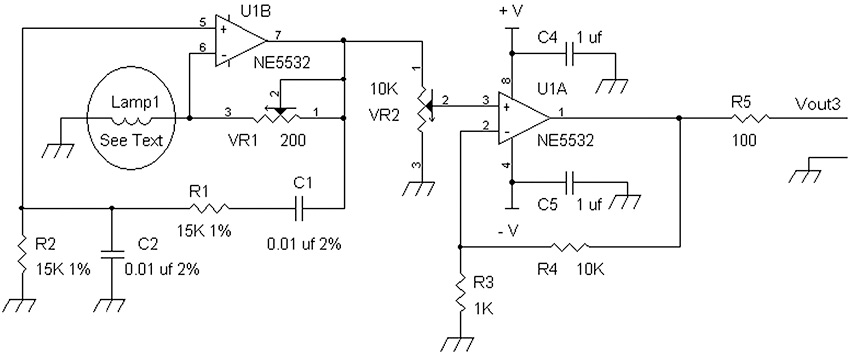
FIGURE 16-1 A Wein sine-wave oscillator circuit from Chapter 9.
The key to oscillation is that there is a 0-degree phase shift at a particular frequency from this positive-feedback network. That is, at the resonant frequency, the network has no j term or reactive component that would cause a non-0-degree phase shift.
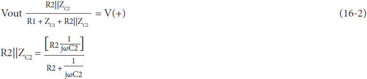
A simplified block diagram of the Wein oscillator is shown in Figure 16-2. For a top-level view, let’s assign the following:

FIGURE 16-2 Block diagram of a Wein oscillator.
Z1 = R1 + ZC1
where ZC1 = 1/jωC1 and ZC2 = 1/jωC2. By way of a voltage-divider formula:

The algebra will be getting messy, so it will be better to show Equation (16-1) in terms of a fraction:
If we multiply by:

we get:
In Figure 16-1, we made the two resistors and two capacitors equal in value, which leads to:

Now, by multiplying by:

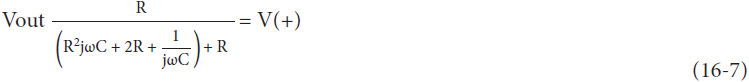
Let’s add the 2R and R terms in the denominator and group the imaginary and real numbers as follows:
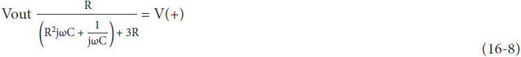
Also note that:

We can now solve for a frequency where the imaginary number goes to zero for a particular frequency ω, which will be the resonant or oscillation frequency. That is:
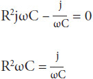
and we can divide by j on both sides to get:
![]()
and if we multiply by ωC on both sides, the result is:
R2ω2C2 = 1 or ω2 = 1/R2C2
Taking the square root of both sides and having only a positive frequency, we have the oscillation frequency as:
![]()
Or in terms of the oscillation frequency in hertz, Hz, we know that:
ω = 2πf
This leads via Equation (16-10) to:
2πf = 1/RC
and by dividing by 2π on both sides, the oscillation frequency in hertz, Hz, is:
![]()
At the oscillation frequency, the reactive component that is associated with the j terms disappears, and the positive-feedback network is described as a purely resistive voltage divider:
![]()
This represents a gain factor of one-third, which is a loss, and to provide an oscillation, we need to make up the loss and have:
![]()
Or put another way, an oscillation occurs when the gain A is ≥ 3 to make up for the losses or attenuation factor of (1/3) due to the positive-feedback network.
Thus A ≥ 3 for a reliable oscillation. For the op amp circuit in Figure 16-1, the gain is:
A = ([VR1/RLamp1] + 1)
where VR1 is adjusted until there is an oscillation, and RLamp is the alternating-current (AC) resistance as the lamp’s filament is being heated. Thus:
A = ([VR1/RLamp1] + 1) ≥ 3
which leads to:
([VR1/RLamp1] + 1) ≥ 3
By subtracting 1 from both sides of ([VR1/RLamp1] + 1) ≥ 3, we get:
[VR1/RLamp1] ≥ 2
Or put another way, the resistance of VR1 has to be at least twice the resistance of the lamp to ensure oscillation.
Before leaving the Wein oscillator circuit, let’s take a look at the magnitude of the positive-feedback voltage divider network from Equation (16-9), which we will call M(ω):

We know at the oscillation frequency ω = 1/RC that M(ω) = M(1/RC) = (1/3). At frequencies where ω << 1/RC, the term 1/ωC dominates by becoming very large in comparison with any of the other terms in the denominator and causes M(ω) → 0. If we look at Figure 16-1 at frequencies below the oscillation frequency, such as close to DC, C1 will block out the signal from the output of pin 7 of U1B.
Also, at frequencies where ω >> 1/RC, the term R2ωC becomes dominant and very large in comparison with any of the other terms in the denominator and again causes M(ω) → 0. Again, intuitively, this makes sense if we look at Figure 16-1, where C2 at high frequencies will behave as an AC short circuit to ground that zaps out any signals from the output of pin 7 of U1B.
From looking at the boundary conditions or the limits of the extremes, as I like to call them, the positive-feedback network has the characteristic of a band-pass filter, which is generally desirable in an amplifier feedback oscillator. The maximum output of the network described by Equation (16-12) occurs at the oscillation frequency, and any other frequency above and below the oscillation frequency will have a smaller output.
A Phono Preamp Revisited
Let’s take a look at the two-stage RIAA (Radio Industries Association of America) phono equalization circuit that was shown in Chapter 8 [see Figure 16-3 (shown previously as Figure 8-12)]. The two equalization networks are implemented by R5 and C5 and by R6, R7, R8, and C9.
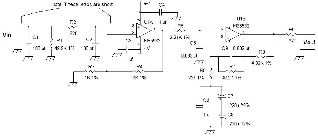
FIGURE 16-3 Two-stage phono preamp from Chapter 8.
From U1A’s output pin 1 to U1B’s input pin 5, R5 and C5 form a frequency-dependent voltage divider that can be described as:
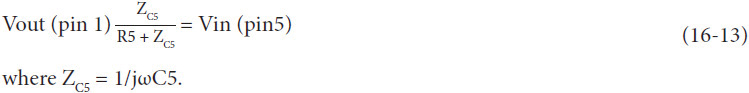
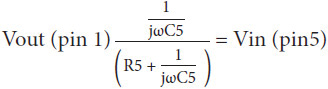
and by multiplying the numerator and denominator by jωC5, we have:
![]()
or, equivalently:
![]()
The magnitude of:

which means that when ω = 1/R5C5:
![]()
The –3 dB cut-off frequency yields a magnitude of 0.707 referenced to a maximum magnitude of 1.0, and its frequency in hertz, Hz, is:
![]()
For this particular example, f ≈ 2.12 kHz, given that R5 = 2.26 kΩ and C5 = 0.033 μF. There is a slight error with R5 = 2.21 kΩ, resulting in f ≈ 2.18 kHz, but it is still close to the 2.12-kHz spec.
At very low frequencies << 1/2πR5C5, ω → 0, and M1(ω) → 1. This makes sense because at DC, capacitor C5 is an open circuit allowing the signal from pin 1 to pass unscathed via R5 to pin 5 in Figure 16-3.
However, at very high frequencies >> 1/2πR5C5, we see that the term gets very large in the denominator of :
![]()
and M1(ω) → 0. Again, this makes sense because at high frequencies, C5 becomes an AC short circuit that grounds pin 5.
For the next network (from Figure 16-3), that is, R6, R7, R8, and C9, we can calculate the gain of the second section with U1B from output pin 7 in reference to input pin 5 as:


At this point, we need to simplify somewhat by bringing out the 1/R6 term, which is a scaler of sorts, and note that R6/R6 = 1. Thus:
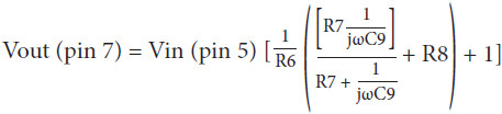
And now the algebra gets a little messy, as if it is not a already a mess. We will multiply R8 by:
to form a common denominator:

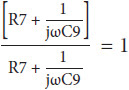
We are almost there—just a few of more steps. We will multiply the numerator and:

If we factor out the term [R7 + R8], we will see that there is an equivalent to two resistors in parallel, R8 and R9, in the numerator:

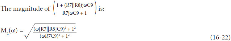
The roll-off frequency associated with R7 is:
f = 1/2πR7C9
and with R7 = 39.2 kΩ and C9 = 0.082 μF, f≈ 49.5 Hz, which is close to the 50-Hz spec. The leveling-off frequency after a roll-off at 49.5 Hz is:
f = 1/2π(R7||R8)C9
and given that R7 = 39.2 kΩ, R8 = 4.32 kΩ, and C9 = 0.082 μF, f ≈ 499 Hz, which is close to the 500-Hz spec.
A Look at an Emitter-Follower Circuit
We now turn our attention to amplifiers, which were covered in Chapter 6. However, I would like to now finally cover them in more detail, especially in terms of input and output resistances, gain, and transconductance.
An amplifier normally includes one or more stages of amplification, where we define amplification as an increase in power gain. This power gain is more easily understood as a voltage or a current gain. In terms of current gain, we can generally associate this with the capability of loading into lower resistances or impedances at the output. For now, we will look at two types of amplifiers—the common emitter and the emitter follower.
In any amplifier, we usually would like to know the AC characteristics in terms of input resistance, gain, and output resistance. The bipolar transistors are described in the following manner: the NPN and PNP transistors are defined by the collector, emitter, and base currents shown in Figure 16-4.

FIGURE 16-4 NPN and PNP transistors with their respective currents.
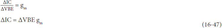
First, let’s take a look at bipolar transistors in terms of their input (VBE) and output (IC) relationships starting with the following equations for NPN and PNP collector currents.
The collector currents are described as:
![]()
![]()
where VT = kT/q = 0.026 mV at room temperature (approximately +25°C), and the number e ≈ 2.71821828. [If you ever want to remember the e approximation, then one way is based on some U.S. history. Andrew Jackson (or Mr. $20 bill) served “2” terms as the “7th” president of the United States and won his first election in “1828.” All this is courtesy of one of my high school math teachers.] Is is the saturation current, which is typically 0.01 pA to 0.0001 pA. VBE is the total voltage, which usually is the sum of two voltages, a quiescent DC bias voltage VBEQ and a small-signal AC signal Vbe:
VBE = [VBEQ + Vbe]
for the NPN transistor, and similarly, for the PNP transistor:
VEB = [VEBQ + Veb]
For now, let’s just look at the NPN transistor. Thus:
![]()
Using the exponential law of a(b + c) = abac, we have:
![]()
When Vbe = 0, we have a quiescent collector current ICnpnQ that is a no-AC-signal condition, resulting in e(Vbe/VT) = e(0/VT) = 1 and:
ICnpnQ = Is[e(VBEQ/VT)] = ICQ
where ICQ is the quiescent DC collector current. With the AC signal Vbe, Equation (16-26) is equivalent to:
![]()
We can make a linear approximation of e(Vbe/VT) because ex ≈ 1 + x, and let x = Vbe/VT. Then:
![]()
![]()
![]()
Let’s relate this to the familiar line equation:
y = mx + b
Let y = ICnpn, m = (ICQ/VT), x = Vbe, and b = ICQ
The slope or gain of the line is:

is defined as the transconductance gm.
However, let’s look at total base-emitter voltage VBE and the small signal across the base emitter Vbe. What is the relationship between ΔVBE and ΔVbe?
VBE = (VBEQ + Vbe) → ΔVBE = Δ(VBEQ + Vbe) = ΔVBEQ + ΔVbe
ΔVBE = ΔVBEQ + ΔVbe
We know that when the “whole” base-emitter voltage VBE changes due to the small signal added to the DC bias voltage VBEQ, VBEQ stays constant. Thus the change in VBEQ is zero. For example, suppose that the transistor is biased to VBEQ = 0.600 volt DC, and the small-signal Vbe is an AC voltage that varies ±10 mV. VBE = 0.600 volt ± 10 mV. The change in VBE is from 0.610 volt to 0.590 volt, or put another way, the change in VBE is ±10 mV, which is exactly the same change in the small-signal voltage Vbe. This leads to:
ΔVBE = ΔVbe
which says that:


For example, if the quiescent collector current ICQ is 1 mA:
![]()
Because gm is directly proportional to ICQ, we can say that at 0.1 mA = ICQ, gm ≈ 3.84 mA/volt, or one-tenth the transconductance for 1 mA = ICQ.
When we look at the curve of the function Ise(VBE/VT) in Figure 16-5, we can see that the slope increases as the collector current increases, thereby increasing gain or transconductance gm.

FIGURE 16-5 Graph of the collector current Ise(VBE/VT) as a function of VBE, where the vertical axis is the collector current and the horizontal axis is the base-emitter voltage.
When the small-signal transconductance gm is known, we can then calculate the output resistance for an emitter follower. For simplicity, we will use a PNP emitter-follower circuit, as shown in Figure 16-6, but the answer will be the same for an NPN emitter follower.

FIGURE 16-6 PNP emitter-follower circuit.
For a PNP transistor, note that we use Veb instead of Vbe. Note from the NPN Equation (16-32) that we can also say for a PNP transistor that ΔVeb = ΔVBE. Thus:

Also, the current gain β = IC/IB, or the ratio of collector current to base current, and IB + IC = IE, the emitter current. We can relate the following:
![]()

This also leads to a relationship between the collector and emitter currents as:
IE/IC = [(β + 1)IB]/[βIB] = (β + 1)/β = IE/IC
or, for AC signals:
![]()
This also says that:
IC = IE[β/(β + 1)]
or, for AC signals:
![]()
We are now ready to measure the output resistance of the PNP emitter-follower circuit in Figure 16-6. What we want to know is:
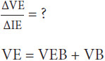
where VEB is the emitter-to-base voltage of the PNP transistor.
![]()
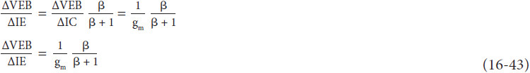
Divide by ΔIE on both sides of the equation to get:
![]()
where Rout is the emitter output resistance.

However:

because VEB represents the DC bias (VEBQ) plus the small-signal voltage Veb, and when we are looking at ΔVEB, the DC bias subtracts out, leaving only ΔVeb. This leads to:
Now we need to know, what is ΔVB/ΔIE?
IE = (β + 1)IB
ΔIE = (β + 1)ΔIB
By Ohm’s law, ΔVB = RsΔIB, so:

![]()
Combining information from Equations (16-43) and (16-44) into Equation (16-40), we arrive at:
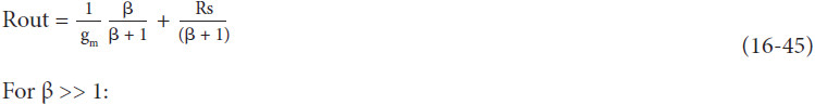
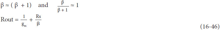
We can now model the emitter follower as shown in Figure 16-6 for AC signals. For Rs = 0 Ω, the gain is unity unless it is loaded to the outside world. This is so because the entire voltage across the emitter-base junction is just VEBQ, the quiescent bias turn-on voltage, and that turn-on voltage acts as a DC level shifter with no change in amplitude to AC signals from the base to the emitter. Note that equations for Rout in Equations (16-45) and (16-46) are applicable to NPN and PNP emitter follower circuits.
Using the Emitter Output Resistance to Determine Characteristics of a Common-Emitter Amplifier
Let’s take a look at the common-emitter amplifier shown in Figure 16-7. It should be noted that in terms of an AC signal across the base-emitter junction, ΔVBE = ΔVbe. To determine the AC collector current with a small signal voltage at the base, Vbe, we can use the transconductance formula for an NPN transistor:
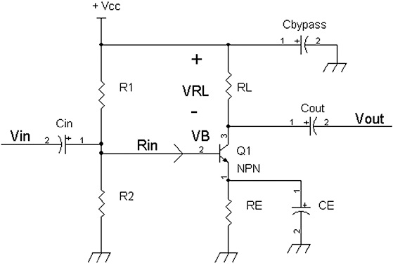
FIGURE 16-7 Common-emitter amplifier with its emitter AC grounded via capacitor CE.
The voltage drop across the collector resistor RL is then:
VRL = ΔIC RL = ΔVBE gm RL = ΔVbe gm RL
Note that VRL is taken from the (+) polarity at Vcc, an AC ground, and the (–) polarity on the collector. If we take the output voltage at the collector referenced to ground, the polarity inverts to:
![]()
The AC signal Vin = ΔVbe, the small signal into the base-emitter junction of Q1. Therefore, the AC gain is:
![]()
The AC input resistance of the grounded emitter amplifier is calculated when we can calculate the input voltage divided by the base current:

The transconductance is defined as the change in collector current over the change in base emitter voltage:
![]()
which leads to:

In general, for signals whose frequencies span many octaves, a grounded emitter amplifier generates too much distortion for input signals exceeding 10 mV peak. A way to reduce distortion is to incorporate a finite resistance from the emitter to an AC ground, as shown in Figure 16-8. To calculate the gain, Vin = VB, and the input voltage source resistance Rs = 0 from Vin.
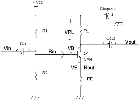
FIGURE 16-8 Common-emitter amplifier with a finite resistance to an AC ground for lower distortion.
From Equation (16-45), the output resistance Rout from the emitter of Q1 is:

However, Rs = 0, and therefore:
![]()
The AC voltage at the emitter:
![]()
and the emitter current is then:
![]()

We can multiply by gm/gm = 1 to get:
and the new transconductance is:
If β >> 1 , then:
![]()
This is a commonly described way of expressing the reduced transconductance due to the finite emitter resistance connected to an AC ground.
However, if we multiply both numerator and denominator by 1/gm, we get an expression that is easier to render quick calculations:
For example, if ICQ = 1 mA, then 1/gm = 26 Ω, and if RE = 470 Ω, which leads to a total of 496 Ω in the denominator:
![]()
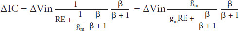
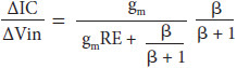
The gain of a common-emitter amplifier with a finite resistance from the emitter to an AC ground is:
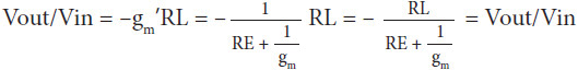
We now turn to calculating the input resistance. Derived from Equation (16-52), we had:

The reciprocal of conductance ΔIC/ΔVin is resistance. This means that ΔVin/ΔIC is a resistance but not yet the input resistance that we want:

To find the AC input resistance, we need to know the ratio of the input voltage to the input base current ΔIB = ΔIC/β. Thus:
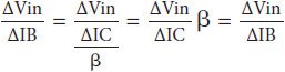
We can multiply both sides of Equation (16-53) by to get ΔVin/ΔIB. Thus:
In a practical example, if β = 100 with RE = 1 kΩ and ICQ = 1 mA, gm ~ 0.038.
![]()
looking into the base of the transistor. As we can see, the resistor RE used for local negative feedback raises the input resistance by quite a bit, and often it results in the the majority of the input resistance with (β + 1) versus the base-emitter resistance β/gm.
Analyzing an Inverting-Gain Video Amplifier
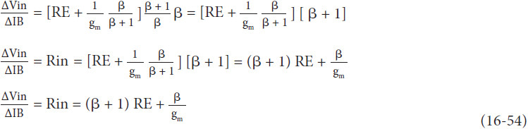
There is one further point we need to add when analyzing amplifiers. In general, most active amplifying devices have current source outputs. When a load resistor is connected to the collector of a bipolar transistor or to the drain of a FET, generally, the output resistance at the collector or the drain is just the resistance of the load resistor. A current source driving current into a resistor forms a Norton circuit that is also equivalent to a Thevenin circuit. The output resistance in the Norton circuit is the same value as the Thevenin resistor (see Figure 16-9).
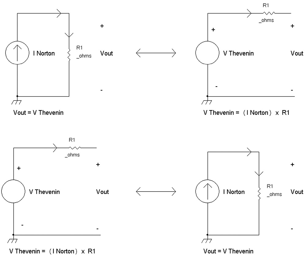
FIGURE 16-9 Norton and Thevenin equivalent circuits.
Let’s now turn to the inverting-gain video amplifier from Chapter 13 (see Figure 16-10). First, we find the DC operating conditions so that we can determine the transconductances for Q2 and Q3. Generally, when the parallel combination of the base biasing resistors (R22 and R23) has a resistance that is less than 20× the 1-kΩ emitter-to-ground resistance of R25, we can assume that there is no DC base current that would pull down the voltage at the base of Q2.
FIGURE 16-10 Video amplifier circuit Q2 and Q3 (originally Figure 13-21).
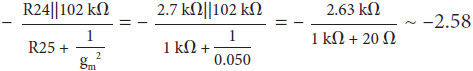
In this case, for R22 = 10 kΩ and R23 = 2.7 kΩ:
R22||R23 = 10 kΩ||2.7 kΩ ≈ 2.1 kΩ < 20 × 1 kΩ = 20 kΩ
The voltage at the base of Q2 is then 9 volts [2.7 kΩ/(2.7 kΩ +10 kΩ)] = +1.9 volts DC. With a 0.6 volt turn-on voltage for Q2 and Q3, the emitter DC voltage at Q2 is 1.9 volts – 0.6 volt = 1.3 volts. With the high current gain β =100, β ≈(β + 1), we can say that the emitter current and collector current of Q2 are the same. Likewise, the emitter and collector currents of Q3 are essentially the same.
With 1.3 volts at the emitter of Q2, the emitter current is then 1.3 volts/R25 = 1.3 volts/1 kΩ = 1.3 mA = IE2 = IC2, where IE2 and IC2 are the DC bias emitter and collector currents. Given 1.3 mA of collector current for Q2, the voltage drop across R24 (2.7 kΩ) is 1.3 mA(2.7 kΩ) = 3.5 volts. The Q2 collector voltage is then 9 volts – 3.5 volts = 5.5 volts DC.
Finally, we need to find the collector current of Q3. Because Q2’s collector voltage is 5.5 volts, and the collector of Q2 is connected to the base of Q3, the base of Q3 also has 5.5 volts DC. Hence the Q3 emitter voltage is 5.5 volts – 0.6 volt (Q3 turn-on voltage) = 4.9 volts DC. The Q3 emitter current is then 4.9 volts/R26 = 4.9 volts/1 kΩ = 4.9 mA. Because the current gain is 100, which is >> 1, the collector current of Q3 is essentially the same as the emitter current. Thus IC3 = 4.9 mA.
Let’s gather what we know so far:
IC2 = 1.3 mA → gmQ2 = 1.3 mA/0.026 V = 0.050 mho (or 50 mA per volt)
IC3 = 4.9 mA → gmQ3 = 4.9 mA/0.026 V = 0.188 mho (or 188 mA per volt)
β = 100
The input resistance RinB into the base of Q2 is:
(β +1)R25 + β/gmQ2 = (101)1 kΩ + 100/0.050 mho = 101 kΩ + 2 kΩ = 103 kΩ
In reality, the input resistance as seen by Vin is a combination of the parallel resistances of R22 and R23 because both resistors go to an AC ground, and RinB is the input resistance to Q2, which is also an equivalent resistance to ground. So there are three resistors from the input terminal that are in equivalent parallel connection. The result is that:
R22||R23||RinB ≈ 10 kΩ||2.7 kΩ||103 kΩ ≈ 2.12 kΩ||103 kΩ ≈ 2.07 kΩ
is the equivalent AC signal resistance as seen by Vin. Input coupling capacitor C19 is considered to be an AC short circuit.
The input resistance to Q3 is:
(β +1)R26 + β/gmQ3 = (101)1 kΩ + 100/0.188 = 101 kΩ + 532 Ω = 101.532 kΩ
Disregarding the input resistance at Q3, which is approximately 102 kΩ >> R24, the AC gain of the first stage from the Q2 collector to the input at the base is approximately:

If the input resistance into Q3 is taken into account, the more accurate gain calculation is:
In both cases, they are very close. For a first approximation, we will just use approximately –2.65 for the voltage gain of Q2.
The output resistance RoutQ3 looking into the emitter of Q3 is approximately:
[R24/(β +1)] + (1/gmQ3) ≈ 2.7 kΩ/101 + 1/0.188 mho ≈ 26.7 Ω + 5.3 Ω ≈ 32 Ω = RoutQ3
The model for Q2 and Q3 is shown in the block diagram in Figure 16-11.

FIGURE 16-11 An approximate representation of the amplifier shown in Figure 16-10.
It should be noted that the hand calculations are usually sufficient to get a feel for the DC biasing currents and voltages along with the AC gain of the amplifier. For more accurate answers, one can calculate further with more exacting models, but at that point, it is probably easier to download a free circuit simulation software pack such as LTSPICE by Linear Technology at www.linear.com/designtools/software/.
If base currents are sufficiently significant as to affect the operating point of a previous resistive network such as the base current in Q3 pulling down the collector voltage of Q2, then the calculations become a lot more involved, and there are a few options one can take. One is to design the previous stage’s resistance values low enough so that the base current of Q3 is insignificant, which is preferable, or the second option is to go through the longer calculation for the worse-case current gain and determine whether the amplifier will still work within expectations. The third is to build or simulate the circuit. When I designed the inverting video amplifier in Chapter 13, I deliberately chose smaller-value resistors for biasing (R22 and R23) and loading (R24) such that I did not have to worry about base currents affecting the bias point significantly.
Improvements or Variations of Previous Projects
Sometimes one can improve existing projects by replacing one part with a completely different part or by adding a few parts. We will start with an improvement of the superheterodyne radio that used a TA7642 chip (see Figure 16-12).

FIGURE 16-12 Modified circuit by replacing the 470-pf capacitor originally between the two IF transformers with ceramic filter CF1 (e.g., SFU455KU2-B0).
By adding almost any ceramic filter as shown, the selectivity of the AM radio goes up. A 455-kHz ceramic filter (e.g., Murata Part Number SFULA455KU2A-B0, which is available at www.mouser.com, or, alternatively, the SFULA455KU2B-B0) generally is equivalent to adding one or two more intermediate-frequency (IF) transformers. With this modification from the Bay Area, the radio was able to receive radio station KFI from Los Angeles and adjacent channel interference was were very well filtered out. Selectivity was noticeably improved, even though the SFULA455KU2A-B0 ceramic filter has a “normal” bandwidth of 10 kHz. Other 455-kHz ceramic filters are also available, and some have multiple sections for sharper selectivity. These can be tried as well.
Another modification that is relatively easy is to add gain in the IF system for an FM radio to increase its sensitivity. In the FM tuner using the TA2003 integrated circuit (IC), one improvement was to connect two 10.7-MHz ceramic filters in series for increased selectivity. We can add a common-emitter amplifier (R5, R6, Q1, R3, R4, and C10) in between the two filters, as shown in Figure 16-13, to make up for losses in the ceramic filters and thus provide a bit more sensitivity. Note that an extra supply bypass capacitor C11 is added to this amplifier supply line.

FIGURE 16-13 A one-transistor amplifier is placed between F1 and F2 for improved sensitivity.
The gain of the amplifier assumes a 330-Ω input resistance into the second ceramic filter F2, so the effective collector load to Q1 is 330 Ω||330 Ω, or 165 Ω. The DC collector current is about 0.8 mA → gm = 0.8 mA/0.026 V = 0.0307 mho. The gain of the added common emitter amplifier is then = –gm(165 Ω) = –0.0307 mho(165 Ω) ≈ –5.
Just for Fun … A Wein Oscillator Using a 60-Watt Light Bulb
In Chapter 8, various types of low-voltage lamps were used as a nonlinear variable resistor to allow the Wein oscillator to achieve a steady-state-amplitude sine-wave signal without clipping. I later tried larger 120 volt bulbs starting from an 11-watt bulb to as much as 60 watts, and the success rate was not as good as using the lower-voltage bulbs. What happened was that the amplitude was not stable and tended to “breathe.” It occurred to me that in some of the Wein oscillators, such as the HP 200, the lamp is connected between the cathode of the first tube and ground. The tube is DC biased for a particular cathode current, resulting in a slight DC current flowing through the lamp as well as (having) an AC signal across it. So, to improve the Wein circuit such that it worked with higher-voltage and higher-wattage lamps, I decided to add a prebias circuit (R6A to R6C) as shown in Figure 16-14 and the completed project in Figure 16-15.
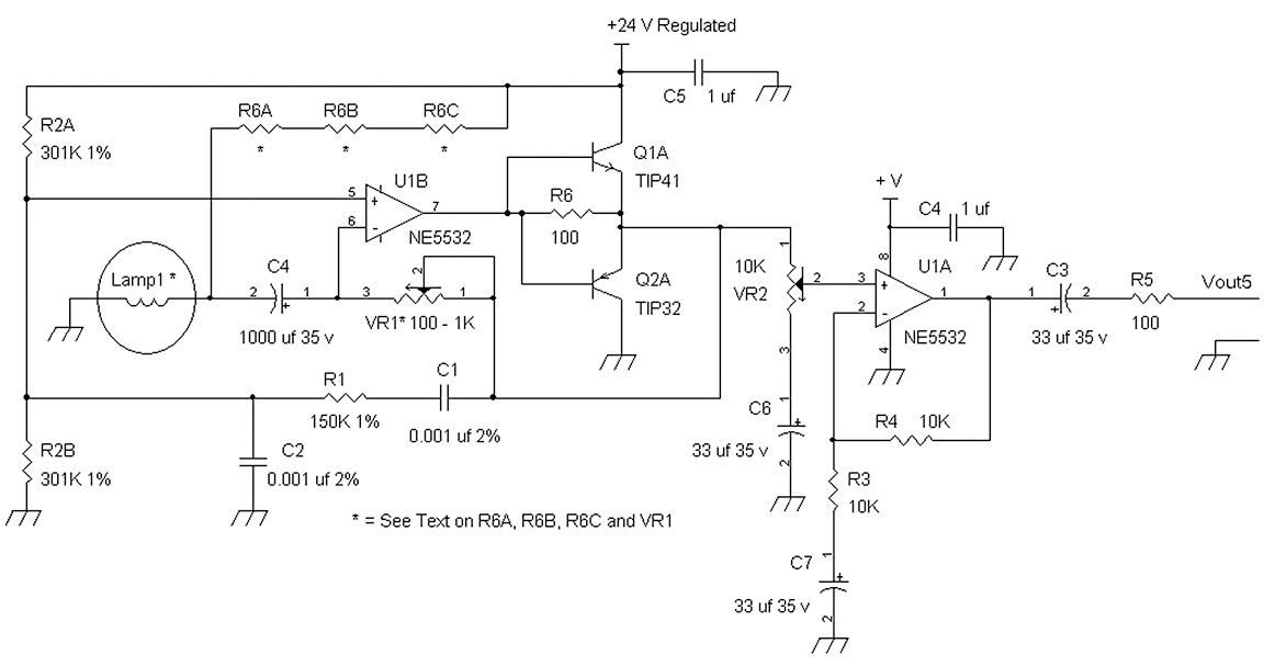
FIGURE 16-14 Wein oscillator with added DC current to provide better amplitude stability.
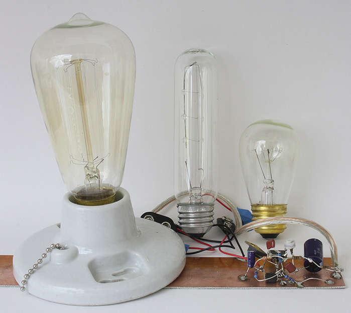
FIGURE 16-15 The 60-watt light bulb Wein oscillator with a Feit old style 60-W lamp installed in the socket with Philips 25-W tube and 11-W clear bulbs behind.
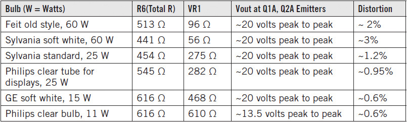
The circuit works well enough to provide a reasonable sine-wave signal, and the prebiasing resistors R6A to R6C reduce or eliminate low-frequency amplitude modulation on the output signal. Note that a regulated 24 volt supply is recommended, such as using a raw 30 volt DC supply and connecting it to a 24 volt regulator chip such as the 7824 (TO-220 package). Biasing resistors R6A, R6B, and R6C are ¼-watt resistors and can be replaced with a single 1-watt resistor. Gain-control potentiometer VR1 may be 100 Ω when used with a standard 60-watt soft white light bulb. Some other 60-watt lamps may have higher resistances and VR1 → 200 Ω. However, because of the amount of power that is dissipated by VR1, it is recommended that at least a ½-watt or 1-watt variable resistor is used. Other types of bulbs may be used; see Table 16-1 for a summary. Note that R6(total R) = (R6A + R6B + R6C).
TABLE 16-1 Summary of Various Lamps Used for the Wein Oscillator
A Brief Study on Harmonic Distortion Analysis
This section is optional because this subject is generally taught in very advanced courses in electronics. However, the results of the analysis show that common-emitter amplifiers such as those used in RF (radio-frequency) mixers and fuzz boxes do generate quite a bit of distortion.
For a single-transistor NPN common-emitter amplifier with the emitter AC grounded, the collector current equation is described again by Equation (16-27):
The e(Vbe/V T) function can be more characterized beyond a linear approximation as highlighted in boldface in the following:

NOTE n! = (n)(n – 1)(n – 2) L (1). For example, 5! = (5)(4)(3)(2)(1) = 120, and 3! = (3)(2)(1) = 6.
If we are just interested in second- and third-order distortions from Equation (16-27), we plug in a1 = 1, a2= ½, and a3= ⅙ into Equation (16-55) and combine it with Equation (16-27) to get:
![]()
For a sinusoidal input signal, we let the AC signal = B cos( ωt) = Vbe, and Equation (16-56) becomes:

The harmonic distortion is the ratio of the amplitudes of the harmonic signal to the linear term signal (B cos(ωt)/VT) that has the fundamental frequency, ω.
For the second harmonic term, let’s take a look at:
(1/2)(B cos(ωt)/VT)2 = 0.5 (B cos(ωt))2(1/VT)2
and:
(B cos(ωt))2 = (0.5)B2[cos(2ωt) + 1](1/VT)2
Note that squaring the input signal results in a second harmonic and a DC term. In particular, we get a (0.5)B2 cos(2ωt) second-harmonic term. We can now say that:
(1/2)[Bcos(ωt)/VT]2 = 0.5(0.5)B2[cos(2ωt) + 1](1/VT)2
The ratio of the second-harmonic signal to the fundamental-frequency signal is:
0.5(0.5)B2[cos(2ωt)](1/VT)2/[B cos(ωt)/VT]
but we are only interested in the amplitude 0.5(0.5)B2(1/VT)2 of the second-harmonic signal and the amplitude (B/VT) of the linear term to determine the distortion. The second-harmonic distortion HD2 is then:


What this says is that if the peak sinusoidal voltage B is even as small as 1 mV, then the second-order harmonic distortion is approximately 1/100 ≈ 1 percent. Equation (16-59) also says that HD2 is directly proportional to the amplitude of the input signal, which equates to 1 percent per 1 mV peak signal. For example, if the input signal is 3 mV peak, we would expect about 3 percent second-harmonic distortion.
The third-harmonic analysis gets a bit more messy, so I will refer to Robert G. Meyer’s EE140 and 240 notes from 1975 and 1976. Thus:
![]()
Note that HD3 is proportional to the square of the input voltage. A sine wave at B = 1 mV peak, HD3 ≈ (1/24)(0.001/0.026)2 = 0.00616 percent. However, if B → 10 mV peak, HD3 → 0.616 percent, which is a dramatic increase.
In summary, for second- and third-order distortions we have:
![]()
![]()
where B is the peak input amplitude for a sinusoidal signal, and the base of the transistor is driven by a pure voltage source—a situation where there is no series impedance between the input voltage signal source and base.
From either Equation (16-61) or Equation (16-62), it would appear that if the input amplitude exceeds 1,000 mV peak, the amplitude of the second-harmonic distortion signal will be larger than the input signal by about 10×, and the third-harmonic signal will be larger than the input signal by approximately 61×. Is this possible? The answer is no because at some point with a large amplitude for Vbe, the polynomial approximation for e(Vbe/V T) blows up and is no longer valid.
In fact, if a large-amplitude sinusoidal signal (e.g., 1,000 mV peak) is driving the base-emitter junction of a transistor, the collector output current will approach a narrow periodic pulse having the fundamental frequency. This means that the amplitudes of the fundamental frequency and harmonics will tend to be equal.
For example, in calculating second-order distortion with a polynomial, the inaccuracies begin when the peak amplitude of the input sine wave approaches one VT or 26 mV peak for approximately 26 percent HD2. Beyond 26 mV peak, a more accurate assessment of the second-order distortion can be achieved by using modified Bessel functions instead of the power–series/polynomial method.
Using Differential Gain as a Method to Determine Harmonic Distortion
Based on a general power-series expansion equation, Professor Robert G. Meyer derived formulas to calculate distortion products based on differential gains. The basis is that there is a relationship between variations in gain during the sinusoidal output swing. Using this method allows us not only to calculate distortions for bipolar transistors with emitters that are AC grounded, but it also works well in determining distortions in amplifiers with negative feedback.
It should be noted that any distortion analysis based on power-series expansion requires that the distortion be small and the input-output characteristic have a smooth curve without any abrupt jumps in value. For example, when the amplifier clips or exhibits crossover (aka deadband) distortion, this method is not applicable.
When we look at transconductances of the following:
![]()
for an AC-grounded emitter amplifier and:
![]()
for a common-emitter amplifier with a finite resistance from emitter to ground, we see that the transconductances are a function of the DC quiescent collector current ICQ. As the signal swings above and below ICQ, the transconductance changes. In the case of:
![]()
the transconductane ΔIC/ΔVBE is directly proportional to the collector current. With a form of negative feedback, the other case of:
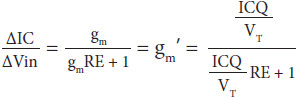
the transconductance ΔIC/ΔVin is not as directly related to ICQ.
So here are paraphrased formulas based on Professor Meyer’s EE140 notes:
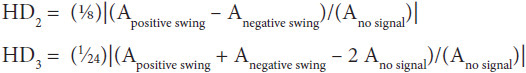
where Apositive swing, Anegative swing, and Ano signal may represent the gain in terms of current, voltage, or transconductance.
The really cool thing about using the differential-gain method is that it analyzes distortions in amplifiers where the current gain β is varying as a function of collector current. Also, this method is applicable to determining distortion in multiple-stage amplifiers with or without feedback, push-pull amplifiers including differential pairs, FET devices that exhibit the body effect, and so on.
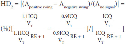
Let’s again take a common-emitter amplifier with its emitter AC grounded and test for second-order harmonics based on an AC signal of 1 mV peak. Thus:
![]()
We need to calculate three collector currents, when Vbe = –1 mV, 0 mV, and +1 mV. The ICQ term will eventually cancel out and is independent of distortion in this case because there is no negative feedback. VT ≈ 0.026 V and gm = ICQ/VT. Thus:
HD2 = (⅛)|(gm(+) – gm(–))/(gm)|
Since gm is directly proportional to ICQ and HD2 (including HD3), it is the ratio of tranconductances, HD2 (and HD3) can be equivalently expressed as a function of ICQ. This leads to:
HD2 = (⅛)|(ICQ e(0.001/V T) – ICQ e(–0.001/V T))/(ICQ e(–0.000/V T))|
HD2 = (⅛)|(1.039211 – 0.962269)/(1)|
HD2 ≈ (⅛)(0.077) = 0.96%
From Equation (16-61), HD2 ≈ B/0.104 V, with B = 1 mV peak; thus HD2 ≈ 0.001/0.104 ≈ 0.96%. So there is a match between using the differential gain and power-series analysis.
Using differential-gain analysis again for calculating HD3 with 1 mV peak signal, we can take the calculations we already have and change the sign from subtraction to addition, but do not forget to add a minus 2 times the zero signal gain, –2ICQ e(–0.000/V T), to the numerator and change the ⅛ factor to 1/24 to get:
HD3 = (1/24) |(ICQ e(0.001/V T) + ICQ e(–0.001/V T) – 2ICQ e(–0.001/V T))/(ICQ e(–0.000/V T))|
HD3 = (1/24) |(1.039 + 0.962 – 2.00)| ≈ 0.001479/24 ≈ 0.00616%
From the power-series Equation (16-62), HD3 = 0.00616% for a 1 mV peak sine-wave signal, which is in agreement with the differential-gain method.
For an amplifier with feedback, one way to use the differential-gain method is to determine the output swing, which is still sinusoidal in nature, and determine the changes in collector current. For example, a common-emitter amplifier with an unbypassed emitter resistor that has a collector current swing of ±10 percent ICQ will be set up in the following manner for calculating second-order distortion. Note that ICQ does not cancel out and does play a role in the amount of distortion (e.g., the higher the ICQ, the lower is the distortion). Thus:
From feedback equations via the Professor’s Meyer’s EE140 notes, the same common-emitter amplifier has the following characteristics of second-order distortion as a function of the input signal:
HD2 = (¼)(B/VT)/(1+gmRE)2
But note that as the distortion is reduced by (1+ gmRE)2, the gain is reduced by (1 + gmRE) via:
![]()
References
1. Robert G. Meyer, “EE140 Notes,” University of California, Berkeley, CA, 1975.
2. Robert G. Meyer, “EE240 Notes,” University of California, Berkeley, CA,1976.
3. Allan R. Hambley, Electrical Engineering: Principles and Applications, 2nd ed. Upper Saddle River, NJ: Prentice-Hall, 2002.
4. Paul R. Gray and Robert G. Meyer, Analysis and Design of Analog Integrated Circuits, 2nd ed. New York: Wiley, 1984.