
CHAPTER 17
![]()
Hacking, Inventing, and Designing
In the context of this book, the term hacking will be defined as modifications or investigations of hardware circuits and systems. For example, an electronic device is taken apart for investigation. The parts revealed within the device can save time in finding the right components for making other types of circuits. Throughout the book so far we have shown examples of hacks, such as taking apart a AA cell to make a flashlight or using a power rectifier (1N5400 series) as a varactor tuning diode. In this chapter, we will look at tearing apart a battery tester and modifying it for something else.
We will also touch on inventing and designing. The term invention includes a novelty of ideas. These ideas can be an improvement of existing ideas, or they can be wholly new. Also, ideas that lead to unexpected results are generally patentable. While showing some examples of inventions, we will also show the design aspects of such inventions.
Hacking
Let’s start with a battery tester bought at Harbor Freight for about $3 (Figure 17-1). The mystery is how does the light-emitting diode (LED) that requires 1.7 volts to light up work when this device tests NiMh batteries that provide only 1.25 volts?

FIGURE 17-1 Three-LED battery tester for 1.5 volt and 9 volt batteries.
It looks like we will have to break open the battery tester to find out how this device works (Figures 17-2a and 17-2b). When the voltage is measured across C2 (see Figure 17-4a), whose positive terminal is connected to the cathode of diode D1, we get about 4 volts. The 33-μH inductor L1 provides an approximately 160 kHz pulse waveform to the anode of D1. We can use this battery tester as a DC-to-DC step-up converter. Although we can just obtain a switching regulator integrated circuit (IC), coil, and Schottky diode, by the time we purchase all these components, we would have spent more than $3 in time and transportation.

FIGURE 17-2 (a) Top side of the battery tester’s circuit board showing a 33-μH inductor L1 and Schottky rectifier D1. (b) Bottom side of the device showing a multitude of surface-mount components including transistors, diodes, resistors, and an LM324 quad op amp U1.
Because this device tests batteries, there are load resistors connected across a crude voltmeter that has three voltage ranges to denote “Replace,” “Weak,” and “Good” conditions of the tested battery. We will have to locate R1 and R4 marked “120” (12 Ω) connected to the 1.5 volt terminals of the battery tester. Once we remove them, we can tap out from C2 to provide approximately 3.5 volts to 4 volts direct current (DC) (see Figure 17-3).

FIGURE 17-3 Surface-mount 12-Ω resistors R2 and R4 removed and two wires (top left of board) brought out to provide approximately 3.5 volts at approximately 30 mA.
The supply of approximately 3.5 volts DC is handy to power a white LED that normally turns on at about 3 volts. We should add a 47-Ω series resistor for current limiting to the white LED. Also with approximately 3.5 volts, we can power op amp and amplifier circuits. Low-voltage op amps such as the LM324 (quad), LM358 (dual), and the faster FET op amps TLC274 (quad) and TLC272 (dual) will work fine at about 3.5 volts. Other op amps, such as the single op amp rail-to-rail versions LMV118 or the Max4321, can be used.
But what if we need to boost the voltage further? We can use our friend the DC restoration circuit and double the original voltage Vout_1 = ~3.5 volts to about 7.5 volts DC for Vout_2 (see Figure 17-4b).

FIGURE 17-4 (a) Partial schematic of the battery tester’s original circuit. (b) Partial schematic of the battery tester’s switching converter that is converted for double voltage by adding external components D_ext 1, D_ext 2, C_ext1, and C_ext 2. (c) Modifications to the battery tester to provide about 7.5 volts DC from a 1.5 volt battery.
Of course, if we want more current, we can hack the LED flashlight in Figure 2-33 (Figure 17-5a). In this hack, we could use the printed circuit board or we can trace down which IC was used. The switching supply IC is a BL8530 with surface-mount connections (SOT-89). From the data sheet, we can build our own 1.5 volt to approximately 4.5 volt power supply (Figure 17-5b).
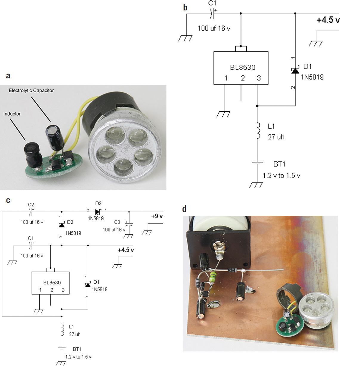
FIGURE 17-5 (a) LED flashlight taken apart to reveal a BL8530 IC. (b) Switching power-supply schematic. (c) Schematic of the voltage doubler circuit with the BL8530 chip. (d) Prototype circuit of the BL8530 1.5 volt to about 9 volt converter (voltage doubler) and the original LED flashlight taken apart.
Again, can we boost the voltage? If we use a DC restoration circuit that is part of a voltage doubler circuit, we should be able to boost the voltage (Figure 17-5c and d).
We now turn our attention to a couple of AM/FM radios. The first radio to examine is the RadioShack Catalog Number 1200586 radio, and we will take it apart (Figure 17-6a). There are only two Phillips screws on the back that are removed. One is seen on the back of the case above the “RadioShack” lettering, and the other is hidden inside the battery compartment. Remove the batteries, and the screw is located in the middle. Then we carefully pry open the case.
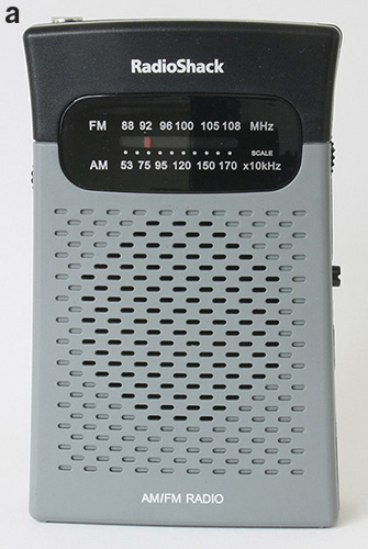
FIGURE 17-6 (a) Front side of the RadioShack radio. (b) Front-side circuit board with two potentiometers and a cylindrical watch crystal. (c) Two surface-mount ICs, a 24-pin Silicon Labs 4820A10 AM/FM tuner chip and an 8-pin TDA2822 two-channel audio amplifier.
The first thing we should notice is just how few parts there are on the top side of the board. What’s more intriguing is that there are two potentiometers, one for the audio level and the other for tuning. Also, notice on the top that there is a watch crystal (32.768 kHz) (see Figure 17-6b).
Let’s now take a look at the other side (Figure 17-6c). While I will not show how to hack into this radio, it should be noted that the Silicon Labs 4820A10 IC can receive other bands, such as SW (shortwave) and FM (frequency modulation) stations below 88 MHz. What’s interesting about this investigation is that we now know a part number for a dual low-voltage audio power amplifier IC (the TDA2822) and that this radio, built in 2014, uses no variable capacitors and no coils that are fixed or variable. In fact, this radio is based on software-defined radio (SDR) technology. The Silicon Lab IC has two input ADCs (analog to digital converters) to process I and Q radio signals. The intermediate-frequency (IF) filtering, AM and FM demodulation, and so on are done with digital signal processing (DSP).
Now let’s take a look at a radio that we can modify, the Sony AM/FM Model ICF-S10MK2 pocket radio. This radio was produced in 2014 and is available at Walgreens and www.amazon.com (Figure 17-7a). There is only one screw hidden in the battery compartment to remove. Take out the lower AA battery from its holder on the back, and remove the screw. Carefully pry apart the case, and note that the FM antenna’s wire may get in the way and have to be temporarily desoldered from the circuit board. Also, the AM ferrite-bar antenna may be glued lightly to the case and can be separated so that the circuit board is free. Also, the two battery wires soldered to the circuit board will have to be temporarily desoldered.

FIGURE 17-7 (a) Sony AM/FM Model ICF-S10MK2 radio. (b) FM ceramic filter that can be upgraded for higher selectivity.
Figure 17-7b shows the circuit board with two three-pin ceramic filters, one for AM (455 kHz) and the other for FM (10.7 MHz). The FM ceramic filter is located just above the Sony IC (integrated circuit). For this modification, we would like to improve the selectivity so that more stations (e.g., in between) can be tuned. We will replace the 10.7 MHz filter with a 110 kHz bandwidth filter, the Murata SFELF 10M7KAH0-B0, or the 180 kHz bandwidth filter, the SFELF10M7HA00. These filters are direct pin-to-pin replacements, and note the orientation of the filter in that the front side of the filter that has its printing is facing out toward the edge of the circuit board.
Typically, most AM/FM radios have 10.7 MHz FM ceramic filters of wide bandwidth such as 230 kHz or 280 kHz. We can replace them with a 180 kHz or even a 110 kHz bandwidth filter. Ideally, if you can get a 150 kHz bandwidth filter, it will work optimally in that it can handle the full frequency deviation of the FM signal without substantial distortion while achieving good selectivity. In practice, though, satisfactory results were achieved with the 110 kHz bandwidth filter in terms of the demodulated signal with an acceptable level of audio distortion.
In terms of improving the AM band selectivity, there are not too many choices today. Most available 455 kHz filters that are a direct pin-to-pin replacement have the same 10 kHz bandwidth as the one that already comes with the radio. One can try multielement 455 kHz filters, but just remember that the input pin to the 455 kHz filter is closest to the band switch or to the unloaded capacitor C13.
Inventions and Patents
When one thinks about invention, Thomas Edison’s light bulb comes into mind. Before the advent of incandescent electric lighting, there were gas street lamps and electric arc lights. So what constitutes an invention?
First, there are three types of invention:
• Utility
• Design
• Plant
Most people are more familiar with the utility patent, such as Thomas Edison’s light bulb or George Westinghouse’s air brake for trains. Almost all high-technology developments these days from circuits, to semiconductor devices (e.g., new types of transistors such as the FinFet), to computers, to software, and so on fall into the category of the utility patent. Design patent examples include distinctive industrial designs of products such as audio cables. For example, the company Monster Cable has many design patents on their various speaker cables. A plant patent example includes plants that are reproduced without genetic seeds via grafts or cuttings. In this chapter, we will be discussing utility patents.
There are various ways of coming up with an invention. One is solving a problem that no one else has been able to solve. For example, the safety pin solves a problem for clipping two pieces of clothing together. Another and just as common way to invent is to use something in one field to solve a problem in another field. For example, one can use ideas from audio circuits to solve problems in the bar-code reader field. Specifically, U.S. Patent 4,740,475 shows an invention for a digital bar code reader for cards imprinted with bar codes. The cards are swiped through the bar code reader. However, because some people may move the card through the reader at a slower than normal rate, the existing bar-code reader circuit may have insufficient signal. By using a trick found in a phono preamp RIAA equalization curve or in an analog tape recorder NAB equalization curve, the problem is solved. A bass boost equalization curve is added to the gain function of the amplifier that results in the capability to read bar codes at a speed 4× slower than the original circuit.
And yet another way to come up with an invention is to produce an unexpected result. A very well-known attorney once told me this hypothetical example: if someone finds out that aspirin can be used to make chickens grow faster, then that idea is patentable, the reason being that aspirin is commonly used as a pain reliever. Therefore, the concept of new use resulting in an unexpected consequence is patentable. The unexpected consequence of this hypothetical example is that the aspirin can be used to make chickens grow faster.
Another way of coming up with a patentable idea is to improve an existing invention. However, if the existing invention’s patent is still enforceable, the original owner of that patent may have to be paid or you may have to be given permission to practice the improved patent.
We will examine three patent examples that will include the design philosophies behind them:
• A circuit using a ceramic filter as opposed to a ceramic resonator in a wide-frequency-deviation voltage-controlled oscillator
• An electronic voltage-controlled variable capacitor without using varactor diodes
• A Class AB output-stage amplifier circuit that uses no thermal feedback diodes or transistors to compensate for the quiescent current of the output transistors
Ceramic Filter Oscillator for Wider Frequency Deviation
Generally, oscillators are designed for a fixed frequency or for a variable range of frequencies. However, what if we want to make a variable-frequency oscillator that will always power up within a known range of frequencies? The problem with an inductor-capacitor oscillator is that the inductor and capacitor need to be chosen with tight tolerances. For example, if we want to build a 455 kHz variable-frequency oscillator, to ensure that the nominal frequency is within 5 kHz, both inductor and capacitor must be within about 1 percent tolerance. While 1 percent tolerance capacitors are available, 1 percent tolerance inductors are generally not common because they come in 5 percent varieties.
If we chose a ceramic resonator or a crystal, we will get very accurate frequencies. However, it is very difficult, if not impossible, to move a crystal oscillator’s frequency beyond a 0.3 percent peak-to-peak range. Ceramic resonators allow for a wider range than crystals in terms of frequency deviation in a variable-frequency oscillator, but what if we want a wider range such as on the order of 0.5 percent peak to peak or more?
Ceramic filters are made to replace IF transformers that provide an IF bandwidth filter. They are not intended to be used as part of an oscillator circuit. In U.S. Patent 5,229,535, wider-frequency-deviation oscillator techniques are created via multiple crystals and ceramic filters (see Figures 17-8 and 17-9). Figure 17-8 shows multiple crystals tuned at slightly different frequencies to form a composite crystal band-pass filter that has a wider bandwidth than a single crystal. This approach achieved the desire result. However, it was desired to design the oscillator with a single element to replace custom-made crystals cut at slightly different frequencies. The idea of a ceramic filter became a possible solution because of its common availability (see Figure 17-9).

FIGURE 17-8 Front page of the patent with multiple crystals to emulate a wider-band filter suitable for a wider-frequency-deviation crystal oscillator.
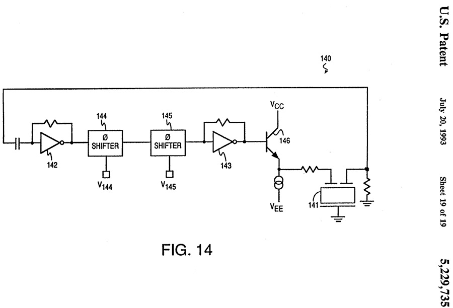
FIGURE 17-9 Example of the use of a ceramic filter for a wide-frequency-deviation oscillator.
A basic premise for using a simple ceramic filter (element 141) is that its phase and amplitude responses are similar to those of a single LC (inductor-capacitor) band-pass filter. What we would like from the ceramic filter is a phase shift on the order of about +90 degrees below the center frequency and –90 degrees above the center frequency. If a multiple-section ceramic filter is used, there may be excessive phase shift, such as ±360 degrees, when the amplitude response is not attenuated, which will lead to oscillation at multiple frequencies. Figure 17-9 shows two inverting amplifiers, 142 and 143, which provide an amplifier with a 0 degree phase shift and voltage gain >1. There are two phase shifters in cascade, 144 and 145, that allow for about double the range of a single phase-shifting circuit. This then provides an increased ability to vary the oscillation frequency.
We now will take a look at practical implementations of ceramic filter oscillators. The first one is shown in Figure 17-10 as the top-level block diagram. An A-to-B dissolve or fader amplifier allows us to continuously mix from 100 percent negative phase signals to 100 percent positive phase signals via the control signal Vcontrol at the base of Q1. With a 50 percent mix, there are negative and positive phase signals that combine to have net effect of 0 degrees phase of shift at the output. Control voltage Vcontrol allows the output of the fader amplifier to provide a signal with adjustable negative and positive phase shifts, including a 0 degree phase shift. The output of the fader amplifier is connected to the input of the ceramic filter. At the output of the ceramic filter, a unity-gain amplifier sends a signal to the lag and lead networks. For the actual implementation, the lag network is a series inductor forming a low-pass filter with the input resistance of the A input. Positive phase via a lead network is provided by a small-value series capacitor to provide a high-pass filter with the B input. An output of the oscillator may be taken from the output of the unity-gain amplifier Q4.
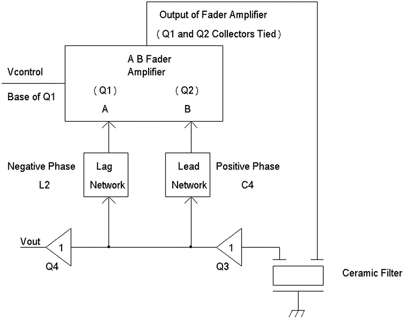
FIGURE 17-10 A 455 kHz ceramic filter oscillator.
Now let’s look at the circuit implementation shown in Figure 17-11. The control voltage to the base of Q1 is provided at the slider of potentiometer VR1. By varying the base voltage of Q1, a mixture of lagging and leading signals via L2 and C4 is provided via the Q1 and Q2 summed collector currents. Q1 and Q2 are current steering devices. The emitter input resistance of Q1 and Q2 is determined by the collector current of each transistor. Emitter resistors R4 and R6 provide a linearized control range. Resistor R5 sets the maximum emitter or collector current. With approximately 4.5 volts at the base of Q2, the emitter voltage is about 4.5 volts – 0.6 volt = 3.9 volts. The emitter tail current is about 3.9 volts/(1 kΩ + 4.7 kΩ) ≈ 0.684 mA. When VR1 is adjusted to have a much higher voltage at Q1’s base than the voltage at the base of Q2, the input resistance into Q1’s emitter is approximately 1/[0.684 ma/0.026 V] = 1/gm ≈ 38 Ω. The input resistance to the emitter of Q2 is nearly infinite resistance because Q2 is nearly turned off while Q1 is almost fully turned on. When VR1 is set to a voltage at the base of Q1 that is much lower than the base voltage of Q2, Q1 is at nearly cut off with nearly infinite emitter input resistance, and Q2 is turned on for an approximate emitter input resistance of 1/[0.684 mA/0.026 V] = 1/gm ≈ 38 Ω. Both Q1 and Q2 are common-base amplifiers that provide the positive gain of >1 required for oscillation. Normally, just R3 would suffice as the load resistor to drive the input of the ceramic filter. However, the 455 kHz ceramic filter includes a spurious response at about 6 MHz. By adjusting VR1, the oscillator will normally provide about ±2.5 kHz of shift. If VR1 is adjusted further for more frequency shift at 455 kHz, a 6 MHz oscillation will occur. A wide-bandwidth, low-Q band-pass filter L1 and C2 provides attenuation at 6 MHz while passing 455 kHz signals with very little effect.

FIGURE 17-11 A 455 kHz ceramic filter voltage-controlled oscillator.
If the input resistance to the ceramic filter is ignored because the bandwidth of the parallel LCR filter L1, R3, and C2 is much wider than the ceramic filter’s bandwidth, the Q is approximately 2π(455 kHz)(R3)(C2) = 2π(455 kHz)(3 kΩ)(560 pF) ≈ 4.8. The bandwidth of the LCR filter is 455 kHz/Q = 455 kHz/4.8 ≈ 94 kHz >> 10 kHz = bandwidth of the ceramic filter CF1 (e.g., Murata SFULA455KU2A-B0).
Base bypass capacitors C3 and C6 ensure that the bases of Q1 and Q2 are AC grounded at 455 kHz to ensure that Q1 and Q2 are (AC) grounded amplifiers for the lag and lead networks L1 and C4. DC blocking capacitor C5 is used so that the DC voltage at the emitter of Q3 does not couple directly DC-wise into the emitter of Q1. Although the output of the oscillator may be taken from the emitter of Q3, an extra emitter follower stage Q4 provides isolation from the outside world so as to minimize any effect of external loading to the oscillator.
For a 10.7 MHz wide-frequency-deviation oscillator, see Figure 17-12. For this oscillator, about ±30 kHz of frequency deviation is provided. The 10.7 MHz ceramic filters of bandwidths from 100 kHz to 230 kHz worked satisfactorily (e.g., Murata SFELF 10M7KAH0-B0 or SFELF 10M7GA00-B0). A 350 kHz wider-bandwidth ceramic filter proved unreliable in providing a single stable frequency. Because there are low amounts of spurious response from the 10.7 MHz ceramic filters, an LC band-pass filter is not required. Thus only a resistive load R3 is required. For a narrower range of frequency deviation, a 20 kHz ceramic filter (Murata Part Number SFKLF 10M7NL00-B0) can be used.
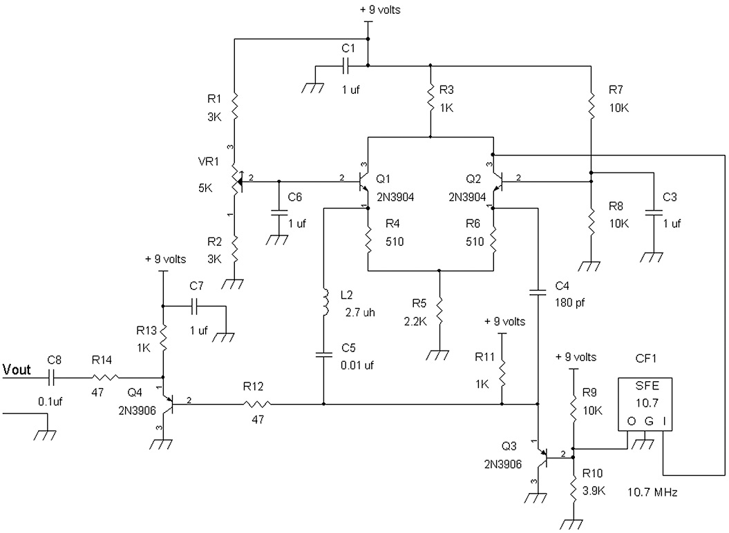
FIGURE 17-12 Ceramic filter 10.7 MHz voltage-controlled oscillator.
Note that the values for L2, C4, R3, R4, R5, and R6 are different in Figure 17-12 from those in Figure 17-11. A higher quiescent current was required for Q1 and Q2 when operating at 10.7 MHz versus 455 kHz.
A Non-Varactor Electronic Variable Capacitor
Varactor tuning diodes are limited in their capacitance, and sometimes an alternative electronically controlled capacitor is desired. To provide some background as to how a nonvaractor electronic variable capacitor works, we need to briefly examine some simple feedback circuits (Figure 17-13).

FIGURE 17-13 Circuits, (a) through (d), with each an input voltage V and a resulting input current I.
The circuit in Figure 17-13a shows a voltage source V connected to a resistor R1. If we want to determine what the equivalent resistance seen by the voltage source is, we can measure the current I. For example, the voltage across R1 is V, and the resulting current is V/R1 = I.
The equivalent input resistance is Rin = V/I = V/(V/R1) = R1. By inspection, one can see right away that Rin will be equal to R1, but we will find out shortly that using V/I is very useful for finding equivalent resistances, capacitances, and inductances.
The next question is, what is the equivalent input resistance when resistor R1 is connected as a feedback resistor for a negative-gain amplifier? In Figure 17-13b, we will also determine Rin via V/I. The trick is figuring out what the input current I is.
NOTE For all of the inverting-gain amplifiers shown in Figure 17-13b through 17-13 d, the input resistance is infinite into the amplifier itself. Therefore, all the current I will be flowing through R1, C1, and L1.
For the circuit in Figure 17-13b, the input of the amplifier has a voltage V at the input, and thus the output voltage Vout = –AV. The voltage across R1 then is V – (–AV) = V + AV = V(1 + A). The current I is then the voltage across R1 divided by its resistance R1. We have I = V(1 +A)/R1, and we can substitute this into Rin = V/I = V/[V(1 + A)/R1] = 1/[(1 + A)/R1] = R1/(1 + A)= Rin.
What this says is that if the gain A = 0, Rin = R1 because Vout will be 0 volt or ground potential. But if A = 1, Rin = R1/2. For example, if R1 = 10 kΩ and –A = –1 so that A = 1, Rin = 10 kΩ/(1 + 1) = 10 kΩ/(2) = 5 kΩ. Having a feedback resistor with a finite-gain amplifier results in having a lowered equivalent resistance. Put another way, if V = 1 volt and –A = –1, then Vout is –1 volt, and there are (1 volt – –1 volt) = 2 volts across R1, or 2× more current flowing through R1 than if R1 were grounded and had 1 volt across it. The output of the amplifier causes more current to be drained at the input and thus simulates a lower input resistance. Because the resistor current is increased by a factor of (1 + A), the equivalent resistance as seen by the input source V is R1/(1 + A). In Figure 17-13b, Rin = R1/(1 + A). This means that if we were able to vary the gain of the inverting amplifier, we could change the input resistance without having to change R1’s resistance value.
Now let’s examine what happens when there are feedback capacitances and inductances when the voltage source V provides a sinusoidal signal in Figure 17-13c and d. For a capacitor, the impedance is ZC1 = 1/jωC1. The voltage across C1 is then (V – Vout) = V – (–AV) = (1 + A)V = voltage across C1. The AC current due to the voltage across C1 is I = (1 + A)V/ZC1.
The input impedance Zin = V/I, which will eventually tell us what the input capacitance Cin is. Thus:
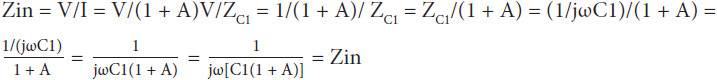
If the inverting gain is 0, A = 0, so Zin = 1/(jωC1), which tells us that Cin = C1.
But for any nonzero gain A, we see a multiplied capacitance because the input impedance is:
![]()
This means that the input impedance is purely capacitive and that capacitance is:
Cin = C1(1 + A)
which means that there is an equivalent capacitance referenced to ground that is a multiplied version of C1. For example, if C1 = 100 pF and –A = –99 so that A = 99, then:
Cin = (1 + 99)100 pF = 10,000 pF.
Also, by changing the gain of the inverting amplifier, we can provide the equivalent of a variable capacitor. This makes sense because there is more AC current flowing through C1 when there is an out-of-phase signal at Vout. The unexpected increase in current is equivalent to having an increased capacitance.
In musical effects devices such as a wah-wah circuit, a foot pedal variable resistor changes the gain of an inverting amplifier. A feedback capacitor is used such that a variable capacitor that depends on the foot pedal position changes the frequency and phase response of the wah-wah circuit. Generally, an inductor is connected to the inverting amplifier’s input and ground to form a parallel LC circuit, where the C comes from a configuration similar to Cin shown in Figure 17-13c.
Before we get to the voltage-controlled variable capacitor, let’s take a quick look at Figure 17-13d. The input impedance is Zin = V/I, where the impedance of an inductor is ZL1 = jωL1. Again, we have Vout = –AV. Thus the voltage across L1 is (V – Vout) = [V – (–AV)] = (1 + A)V. Thus:
I = (V – Vout)/ZL1 = (1 + A)V/ZL1
V/I = Zin = V/(1 + A)V/ZL1 = 1/(1 + A)/ZL1 = ZL1/(1 + A) = jωL1/(1 + A)
= jω[L1/(1 + A)]
Zin = jω[L1/(1 + A)]
Zin is purely inductive and has a new inductance value of L1 divided by (A + 1), which is similar to resistances. In other words, the input inductance Lin = L1/(1 + A). For example, if –A = –19, then A = 19, and if L1 = 100 μH, then Lin = 100 μH/(1 + 49) = 2 μH.
Again, note that if the inverting amplifier changes gain, then we can provide a variable inductor that is referenced to ground. Now the question is, what type of amplifier do we use if we want to make an electronically controlled variable resistor, capacitor, or inductor?
First, we have to determine how large the input signals are. For audio signals, the typical amplitudes are greater than 100 mV peak. For some radio-frequency (RF) signals, the levels can be less than 1 mV peak. In Chapter 16, we examined the distortion characteristics of a common-emitter amplifier. For an AC-grounded common-emitter amplifier, the gain or transconductance is directly proportional to the collector current, which allows a very large range of transconductances, but a 1 mV peak sinusoidal voltage into the base-emitter junction already produces 1 percent second-order distortion. What if we decide to apply local feedback via a finite resistance RE to the common-emitter amplifier to lower the distortion? What happens to the gain or transconductance gm’ with changes in collector current?
gm’ = gm/(1 + gmRE) = 1/[(1/gm) + RE)]
In Chapter 16, we saw that second-order distortion goes down by a factor of 1/(1 + gmRE)2 for any given input signal. For example, if the input signal is a 10 mV peak sine wave, without feedback or RE = 0 equivalent via large emitter bypass capacitor to ground, the distortion would be 10 percent second-order harmonic distortion. If gm = 0.0384 mho for 1 mA of DC collector current and RE = 200 Ω, then the second-order harmonic distortion would be
10%/[1 + (0.0384)(200)]2 = 10%/75 = 0.13% = HD2.
Now let’s see if we can control the gain by increasing the collector current twofold from 1 mA to 2 mA. Note that gm = 0.0384 mho for 1 mA DC and 1/gm = 26 Ω. At 2 mA, gm = 0.0768 mho, and 1/gm = 13 Ω. Note that we are using RE = 200 Ω. Thus:
gm’ = 1/[(1/gm) + RE)]
At 1 mA, gm’ = 1/[(1/gm) + RE)] = 1/[(26 Ω) + 200 Ω] = 0.0044 mho. At 2 mA, gm’ = 1/[(13 Ω) + 200 Ω] = 0.0047 mho.
Increasing the collector current 100 percent (from 1 mA to 2 mA) only increased the transconductance, 1/[(1/gm) + RE)], or equivalent gain from 0.0044 mho to 0.0047 mho, which is about 6 percent. Now we are in a “catch 22” situation because while we can lower the distortion in the common-emitter amplifier, we also linearize gain function such that there is hardly any gain variation when the collector current changes greatly. Of course, this is what we should expect when we lower distortion of an amplifier since the differential gain variation is proportional to second-order distortion; lowering this distortion also lowers the differential gain.
I suppose that one can try using a grounded source or cathode FET or vacuum tube to achieve greater gain variation with acceptable distortion characteristics. But FETs need to be selected because their transconductances vary by quite a bit even within the same part number, and tubes are not as convenient to use because they generally require higher voltages.
One solution to this problem is to use half of a voltage multiplier gain cell as a voltage-controlled amplifier (Figure 17-14). The input capacitance equation from the patent is shown in Figure 17-15.
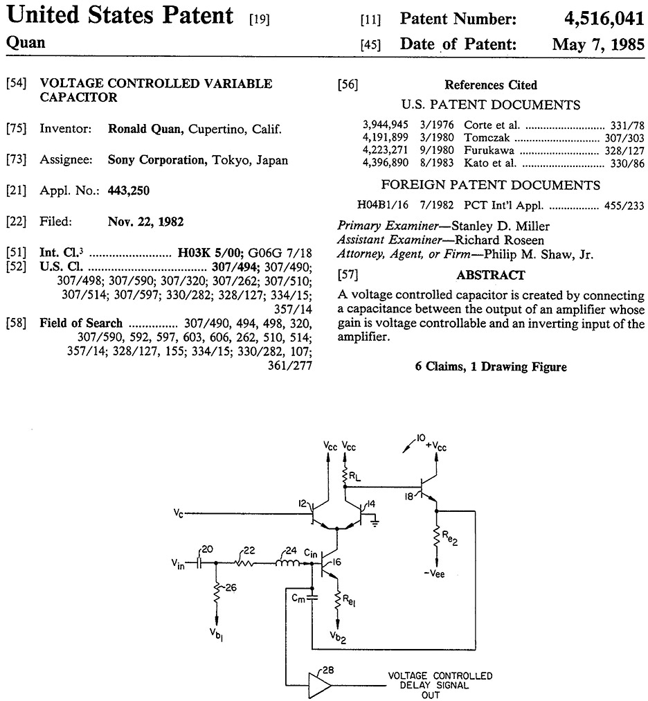
FIGURE 17-14 Front page of U.S. Patent 4,516,041 showing a voltage-controlled variable capacitor.
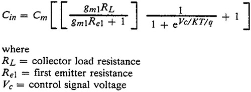
FIGURE 17-15 The variable capacitance described by the equation shown earlier, with an enlarged view of the schematic in Figure 17-16.

FIGURE 17-16 A larger schematic of the voltage-controlled capacitor.
To provide a voltage-controlled variable capacitance looking into Cm, transistor 16 is a common-emitter amplifier with an emitter local feedback resistor to ensure low distortion characteristics. The collector signal current is connected to the emitters of transistors 12 and 14. A voltage-control voltage VC steers the signal current from lower transistor 16 to output transistor 14 or transistor 12, or some mixture of signal current is sent to both transistors. The signal current is proportional to the equation shown in Figure 17-15. When VC = 0, half the signal current goes to transistor 14, and the other half goes to transistor 12. If VC is tipped more positive in voltage, more signal from transistor 16’s collector current will be diverted to transistor 12 than to transistor 14. If VC is tipped more negative in voltage, more signal current from transistor 16 will be diverted to transistor 14 than to transistor 12. Thus transistor 14 provides a gain control of the signal current, and along with load resistor RL, they form a voltage-controlled inverting-gain amplifier. With capacitor Cm, the capacitance Cin is in the form of:
Cin = (1 + A)Cm
where the gain A is a function of control voltage VC. Transistor 18 is an emitter-follower amplifier to provide a low-impedance output stage that drives Cm, which is essential so that the variable capacitance Cin is minimized in resistive losses.
Class AB Output Stage with Quiescent Bias Using a Servo Control
When designing a push-pull output stage, one of the most important circuits is the bias output circuit. Under a no-signal condition, the output transistors are set to a quiescent collector or drain current for bipolar transistors and MOSFETs. Should the bias current be set too low, crossover distortion appears. If the bias current is set too high, steps must to taken so that the output transistors do not self-destruct due to thermal runaway when the DC quiescent current increases until the power dissipation of the transistor becomes too high and exceeds its heat and power ratings.
A common way of providing thermal feedback to an output current bias circuit is to mount biasing diodes or transistors to a heat sink where the output transistors are installed (see Figure 17-17). As shown in Figure 17-17 this audio power amplifier includes output transistors Q4 and Q5 that are typically mounted on a large heat sink. The bias transistor Q3 sets the output quiescent currents of Q4 and Q5 via resistors R5 and R6. Q3 is a VBE multiplier circuit that provides a DC voltage across its collector and emitter of VCEQ3 ≈ VBEQ3(1 + R6/R5) ≈ 0.65 volt(1 + R6/R5). For example, with R6 = R5, VCEQ3 ≈ 0.65 volt(1 + 1) ≈ 1.3 volts.

FIGURE 17-17 A class AB audio amplifier.
By reducing R5’s resistance, we can increase VCEQ3. When the bias for Q4 and Q5 is set to approximately 50 mA or more, these transistors heat up, and the turn-on voltages for Q4 and Q5 drop at a rate of approximately –2 mV/°C. For example, if the rise in temperature is 30°C, the VBE and VEB turn-on voltages for Q4 and Q5 will change by 30 × (–2 mV) = –60 mV for each output transistor. This drop in turn-on voltage of the output devices left without some type of feedback eventually will cause an ever-increasing positive-feedback situation that will result in thermal runaway. By mounting Q3 to the same heat sink as Q4 and Q5, such as Q3 between Q4 and Q5, thermal feedback is achieved. As the output transistors Q4 and Q5 heat up, so does Q3. This then causes the turn-on voltage of Q3, VBEQ3, to also decrease and prevent thermal runaway via VCEQ3 ≈ VBEQ3(1 + R6/R5). It should be noted that emitter resistors R8 and R9 also help in reducing thermal runaway, but their values must be kept low so that the load receives maximum power.
NOTE Because the tabs or cases of Q3, Q4, and Q5 are the collector terminals, care must be taken so that all three transistors are electrically insulated from the metal heat sink.
One question is, can we set the bias of output transistors another way? What was learned in Chapter 13 was that in a video amplifier, we can use a servo or feedback system to ensure that the blanking level of a video signal is set to a reference voltage such as 0 volt regardless of small amounts of DC offsets that may vary in the video signal (see Figure 17-18).
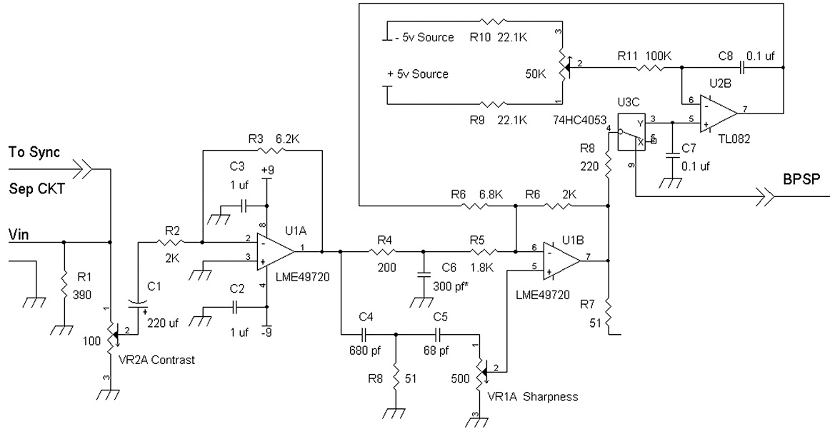
FIGURE 17-18 A feedback clamp circuit for a video amplifier.
A feedback clamp circuit forces the “back porch” voltage of a video signal to a desired voltage set by the 50 kΩ potentiometer (pin 2) connected to R11 in Figure 17-20. A back porch sampling pulse (BPSP) signal activates a sample-and-hold circuit (S/H ckt.), U3C and hold capacitor C7 to store the back porch level of the video signal. The stored voltage is connected to pin 5 of U2B and it is compared with a reference voltage at R11 via pin 2 of the 50 kΩ potentiometer and U2B. An integrator amplifier U2B via pin 7 sends an error voltage to R6 such that the output at U1B has a predetermined back porch level for video signal connected to output resistor R7.
The question is, can we adapt something from video clamp circuits for a new use in amplifiers to set up the bias of the output transistors? Video signals include periodic levels such as blanking levels after the trailing edge of horizontal sync pulses. However, audio signals are generally not periodic in nature. For example, music starts and stops with different notes depending on the program material. So can we adapt some type of video clamp circuit to a class AB amplifier? The answer is yes. See Figure 17-19.

FIGURE 17-19 A block diagram of a servo system similar to a video clamp circuit that sets the output device’s quiescent currents.
A differential amplifier U1 with a collector-current sense resistor Rsense forms a voltage indicative of Q2’s collector current. This voltage is amplified by U1 and fed to the input of the sample-and-hold circuit. The collector current of Q2 changes as the audio signal at Vout is supplied to the load, such as a loudspeaker. However, when Vout is nearly zero in AC voltage, the collector currents of Q1 and Q2 are approximately the same. High-pass filter C1 and R1 passes audio signals from about 16 Hz and up. Because AC signals have to cross 0 volt, we would like to sense the collector current of Q2 only during times when the AC signal at Vout is nearly 0 volt AC.
By using a zero crossing detector, circuit 1 in Figure 17-19, when the audio signal is near 0 volt, the zero crossing detector circuit outputs a high-logic signal to activate the sample-and-hold circuit (circuit 2). The sample-and-hold circuit then stores voltage values only during periods when the AC signal crosses 0 volt DC or when the audio signal is indicative of silence.
These stored voltage values are then voltages indicative of the output transistor’s collector current when the Vout’s AC voltage is zero. The stored voltage value from the sample-and-hold circuit is then compared with a reference voltage set by VR1. An error amplifier that includes an integrator circuit sends a signal to a bias circuit to vary the DC bias for the collector currents of Q1 and Q2.
It should be noted that when there is no audio signal, the zero crossing detector always outputs a logic high, and the sample-and-hold circuit is continuously sampling Vout. With this circuit, emitter series resistors such as R8 and R9 shown in Figure 17-17 are not needed, but they can be included.
Now look at Figure 17-20, which shows the servo-controlled biasing circuit. The output transistors 12 and 14 are tied together at their emitters. A high-pass filter 36 is connected to a zero crossing detector that includes comparators 30 and 32. These two comparators form a window comparator circuit that outputs a logic-high voltage over a narrow range of voltages such as between –20 mV and +20 mV, and it outputs 0 volt for voltages greater than +20 mV and less than –20 mV. The output terminals of the comparators are connected to control sampling switch 34.
FIGURE 17-20 A Class AB output-stage amplifier with a zero crossing detector to set the output collector bias current.
A sense resistor 38 develops a voltage proportional to the collector current of transistor 14. This voltage is amplified by differential amplifier 40. The output of the differential amplifier is connected to the input of sampling switch 34. Switch 34’s output is fed to a hold capacitor and is buffered by voltage-follower amplifier 48, which is connected to inverting amplifier 50. The output of amplifier 50 is fed to an integrator amplifier 52. A reference voltage to set the collector bias current is provided by potentiometer 54 into the (+) input of integrator 52. The output of the integrator amplifier is connected to zener diode 56 to ensure that at startup or power on the biasing circuit does not latch and cause the output transistors to be burned out. Zener diode 56 allows the bias current to start at zero before being increased to the set collector current. The collector biasing circuit includes a variable-current-source circuit via common-emitter amplifier transistor 24, and the voltage developed across resistor 22 then biases the bases of transistors 12 and 14.
When this circuit was built, the quiescent bias current was set and did not change even when the output devices were raised in temperature via a heat gun. However, the circuit did fail, but that was because the heat gun had melted the solder connections, and the transistor terminals eventually became open circuits.
We have now shown three examples of inventions:
• The use of a ceramic filter in an oscillator instead of a resonator
• Application of a differential pair voltage-controlled amplifier for a voltage-controlled capacitor that handles large signals without distortion
• Taking a page from video clamp circuits and varying the circuit a little with a zero crossing detector resulting in the design of a new output stage (the quiescent current of the output devices is set without the use of thermal feedback elements such as diodes or a transistor attached to the heat sink where the output devices are installed)
Other Examples of Designing
We have discussed how relaxation oscillators work. So let’s try a variation on that theme.
Modulating the Power-Supply Pin of an Oscillator to Provide FM
In some of the circuits mentioned using a hysteresis oscillator such as a 74HC14 inverter gate with a resistor and capacitor, it was recommended that the power-supply voltage should be regulated (e.g., +5 volts). However, we can vary the power-supply voltage to the 74HC14 chip to convert it to a VCO (see Figure 17-21).

FIGURE 17-21 VCO made from modulating the power-supply pin of a 74HC14 inverter gate.
The relaxation oscillator including a 74HC14 uses R6 and C6 to determine the center oscillating frequency. To vary the oscillation frequency, one can replace C6 with a varactor diode or a variable capacitor that is electronically controlled. In this circuit, we modulate the power pin 14 of U3A to change the oscillation frequency. Op amp U1A’s output at pin 1 nominally has about 4 volts DC and can vary above and below 4 volts once Vin, an AC signal, is present. Resistor R8 isolates the output of op amp U1A from bypass capacitor C5 to ensure that the op amp does not oscillate due to loading directly to a capacitive load. Output pin 2 of U3A then has both AM and FM. Zener diode ZD1 and transistor Q1 work as positive and negative clipping circuits so that pin 14 of the 74HC14 chip does not suffer from over- or undervoltage. A divide-by-two in frequency flip-flop circuit U4A provides a 50 percent duty-cycle FM signal that also has a stable amplitude signal that is free of AM effects.
An LC RF Matching Network
The concept of an RF matching network using inductors and capacitors is to mimic a transformer for the frequencies of interest. For example, if we want to match a 100-Ω source resistance with a 10 kΩ system, ideally, we would want the equivalent of a transformer with a turns ratio 1/N. Thus:
![]()
That is, if the turns ratio of a transformer from its primary winding to its secondary winding is 1:10 and the secondary winding is connected to a 10 kΩ system, the primary winding of the transformer will have an equivalent resistance of 100 Ω. Thus, if the signal generator’s source resistance is 100 Ω, we will have achieved an optimal power match because the input resistance looking into the primary winding is also 100 Ω.
For an RF matching network to achieve matching from 100 Ω to 10 kΩ, we need to step up the voltage somehow. One solution is to use an LC network, as shown in Figure 17-22. In Figure 17-22, at resonance, we want to choose the values of L1 and C1 such that the voltage source Vlow with source resistance R_low matches the equivalent resistance Rs when C1 is loading down with R_high. If R_high were an open circuit, we would have a series LC circuit, and at resonance, the output voltage of C1 would depend on the driving resistance R_low. For example, if R_low → 0 Ω and R_high → infinite resistance, the voltage across C1 will be very large. This is so because huge currents will flow through L1 and C1 at the resonant frequency where the combination series impedance of L1 and C1 is 0 Ω.

FIGURE 17-22 A low-pass LC network with Q > 1 to provide stepped-up voltage to R_high.
If we load C1 down with a finite resistance R_high, the voltage across C1 at the resonant frequency will be lower because we no longer have as huge currents flowing through L1 and C1. Having resistor R_high in parallel with C1 wrecks the perfect cancellation of impedances with L1.
The question is, how do we find the correct matching network such that when R_high is across C1, Rs looks like R_low, and the voltage at C1 is stepped up by a ratio of ![]() We could start by cranking out impedance formulas for the capacitors, resistors, and inductor with complex impedances, or we could take a look at the circuit backwards and equate the series and parallel LC filter’s Q (see Figures 17-23 and 17-24).
We could start by cranking out impedance formulas for the capacitors, resistors, and inductor with complex impedances, or we could take a look at the circuit backwards and equate the series and parallel LC filter’s Q (see Figures 17-23 and 17-24).

FIGURE 17-23 Looking backwards, we want to find an equivalent Rs such that Rp = R_high.
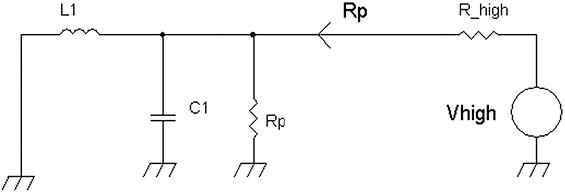
FIGURE 17-24 A resistor in series with L1 is equivalent to a lossless L1 but with an equivalent parallel resistor Rp across C1 and L1.
We will now use the magic of Q, which will be:
Qseries res = (ωr)L1/Rs
Qparallel res = (ωr)Rp(C1)
where ![]() resonant frequency in radians per second. By squaring ωr, we have:
resonant frequency in radians per second. By squaring ωr, we have:
(ωr)2 = 1/L1C1
and by equating Qseries res = (ωr)L1/Rs = Qparallel res = (ωr)Rp(C1):
(ωr)L1/Rs = (ωr)Rp(C1)
Divide by ωr both sides to get:
L1/Rs = Rp(C1)
L1/C1 = RpRs
L1 = RpRsC1, but from (ωr)2 = 1/L1C1, C1 = (1/L1[(ωr)2]), which leads to a substitution for C1:
L1 = RpRs(1/L1[(ωr)2]) = RpRs/L1[(ωr)2]
L1 = RpRs/L1[(ωr)2]
Multiply by L1 on both sides to get:
(L1)2 = RpRs/(ωr)2
Now take the square root of both sides to get:
![]()
![]()
Alternatively by using the formula, ![]() , we also get:
, we also get:
![]()
For example, suppose that we want to match 100 Ω = R_low = Rs to load into 10 kΩ = R_high = Rp, and suppose that the frequency we are interested is approximately 724 kHz, or ωr = 2π(724 kHz). Then:
![]()
With the resonant frequency ωr and L1 known, we can solve for:
C1 = 1/L1[(ωr)2] = 1/(220 μH)[2π(724 kHz)]2 = 220 pF= C1
It should be known that Equations (17-1), (17-2), and (17-3) are accurate when (Rp/Rs) ≥ 10. However, a correction factor can be applied to these equations for more accurate calculations for the matching network in Figure 17-22.
The correction factor is ![]() and this results in:
and this results in:
![]()
![]()
alternatively:
![]()
NOTE The low-impedance side is at inductor L1, and the high-impedance side is at capacitor C1. The matching network looks like Figure 17-22 with L1 and C1.
References
1. United States Patent 5,229,735, “Wide Frequency Deviation Voltage Controlled Crystal Oscillator Having Plural Parallel Crystals,” Ronald Quan, filed March 30, 1992.
2. United States Patent 4,516,041, “Voltage Controlled Variable Capacitor,” Ronald Quan, filed November 22, 1982.
3. United States Patent 4,458,213, “Constant Quiescent Current, Class AB Amplifier Output Stage,” Ronald Quan, filed December 13, 1982.
4. Chris Bowick, John Blyler, and Cheryl Ajluni, RF CIRCUIT Design, 2nd ed. Amsterdam, The Netherlands, Newnes, 2008.
5. David Pressman, Patent It Yourself, 13th ed. Berkeley, CA: Nolo, 2008.