
Appendix A: Logic Gates and Boolean Algebra Used in the Book
This appendix provides a brief set of notes on Boolean algebra laws and their use. It is assumed that the reader already has knowledge of these laws. The appendix is provided as a reference only for the Boolean algebra used in this book.
A.1 BASIC GATE SYMBOLS USED IN THE BOOK WITH BOOLEAN EQUATIONS
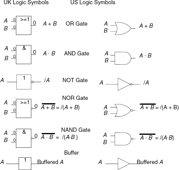
Figure A.1 Basic logic gates.
A.2 THE EXCLUSIVE OR AND EXCLUSIVE NOR
The exclusive OR and exclusive NOR (Figure A.2) are well used in logic systems.
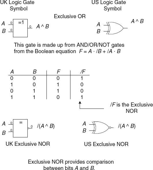
Figure A.2 Exclusive OR and exclusive NOR symbols.
A.3 LAWS OF BOOLEAN ALGEBRA
These are presented in terms of the Boolean logic equation and gate circuit.
A.3.1 Basic OR Rules
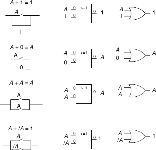
Figure A.3 Boolean algebra basic OR rules.
A.3.2 Basic AND Rules
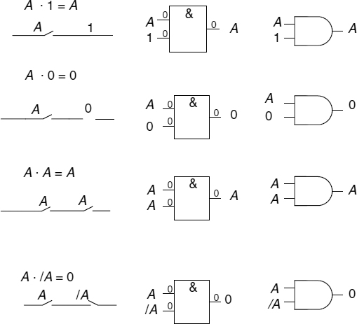
Figure A.4 Boolean algebra basic AND rules.
A.3.3 Associative and Commutative Laws
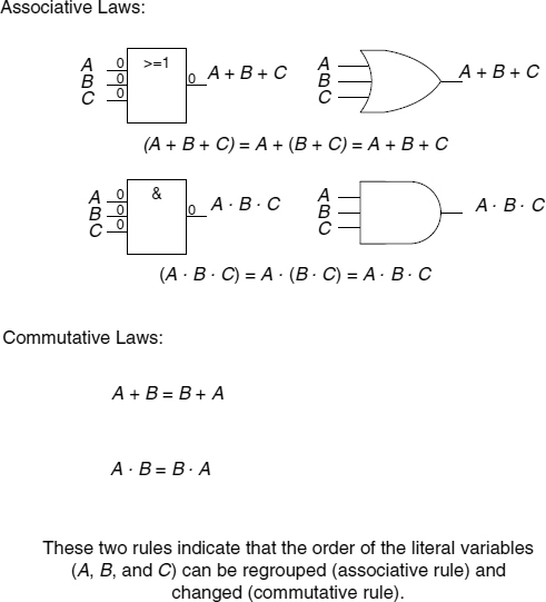
Figure A.5 Associative and commutative laws.
A.3.4 Distributive Laws
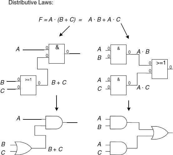
Figure A.6 Distributive laws.
A.3.5 Auxiliary Law for Static 1 Hazard Removal
The auxiliary law (Figure A.7) is particularly significant and much used in this book.
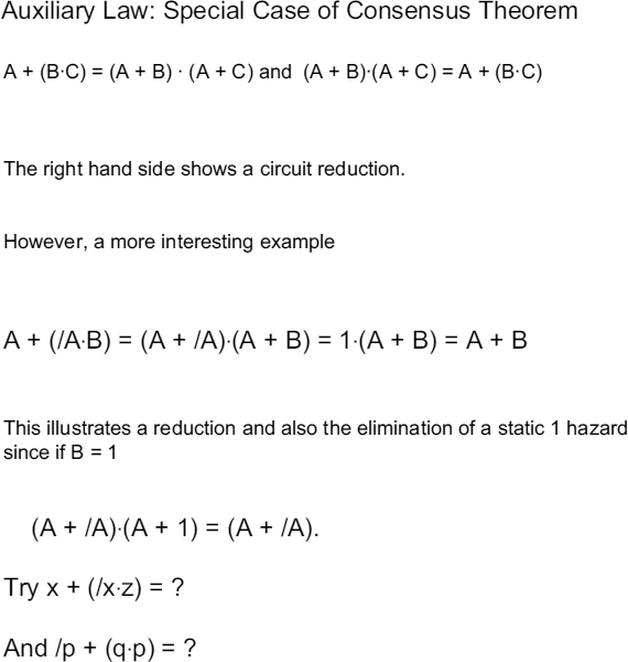
Figure A.7 Auxiliary law.
A.3.5.1 Proof of Auxiliary Rule
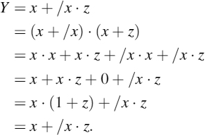
The answer to the first question in Figure A.7 is as follows
The answer to the second question in Figure A.7, /p + (q · p) = ?, is, of course, /p + q. Note that the auxiliary (Aux) rule is just a special case of the consensus theorem.
A.3.6 Consensus Theorem
Consider the equation
Y = x + /x · w · z.
In the equation, if w = z = 1, then
Y = x + /x · 1 · 1 = x + /x,
which is 1.
However, it is possible under some conditions of gate delay that a logic 0 glitch can occur (this is known as a static 1 hazard). To avoid this, a cover term can be added, made up from the literals w and z, to make Y stay at logic 1:
Y = x + /x · w · z + w · z.
Thus, when w and z are both 1:
Y = x + /x + 1,
thus covering the potential terms x + /x and preventing the glitch.
Now consider the equation
Y = x + /xw.
Now add a cover term thus:
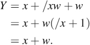
So applying the consensus theorem to Y = x + /xw results in Y = x + w as obtained using the auxiliary rule.
In effect the Aux rule is just a special case of the consensus theorem; that is, it is an auxiliary to the consensus theorem.
Another example (using the Aux rule):
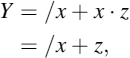
since
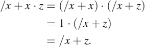
In the following two examples the term to be removed is crossed out thus /R.
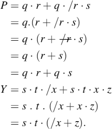
Therefore:
Y = s · t · /x + s · t · z.
Note that the reduction here is in the number of inputs. This might be relevant in some cases, but when implementing with PLD devices it may not be so relevant owing to the large number of inputs available in the AND gate array of the PLD.
Remember, however, that the application of the Aux rule eliminates a static 1 hazard and, hence, a potential glitch: in the case of P, the term r + /r; in the case of Y, /x + x.
A.3.7 The Effect of Signal Delay in Logic Gates
In Chapters 3, 4 and 9, it was shown that signal delay can affect the behaviour of a circuit. The basic effect of signal delay is clearly illustrated in Figure A.8, where the points on the two input signals A and /A where an output change can occur are seen for each gate type.
In the case of AND (or NAND) gates, it is the point at which the two overlapping signals are both at logic 1.
In the case of OR (or NOR) gates, it is the point at which the two overlapping signals are both at logic 0.
The effect is to produce an unwanted glitch at the gate output. These so-called ‘glitches’ can result in maloperation in an FSM. They can occur in a logic system where two signals (they do not need to be the same signals inverted, as shown in Figure A.8) change state at the same time. This could be a change of two state variables; for example, when unit distance coding is not used in a state diagram.
This kind of behaviour can manifest itself within a logic block where two signal changes occur, due to the delays through the logic gates. Further work on this type of behaviour can be found in most textbooks on advanced digital design. These are not discussed any further, as they are beyond the scope of this book.
A.3.8 De Morgan's Theorem
De Morgan's theorem (Figure A.9) is used significantly, particularly in Chapter 9.
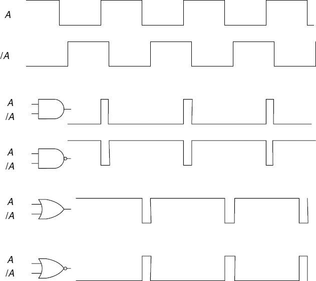
Figure A.8 Effect of delayed signals on gate outputs.
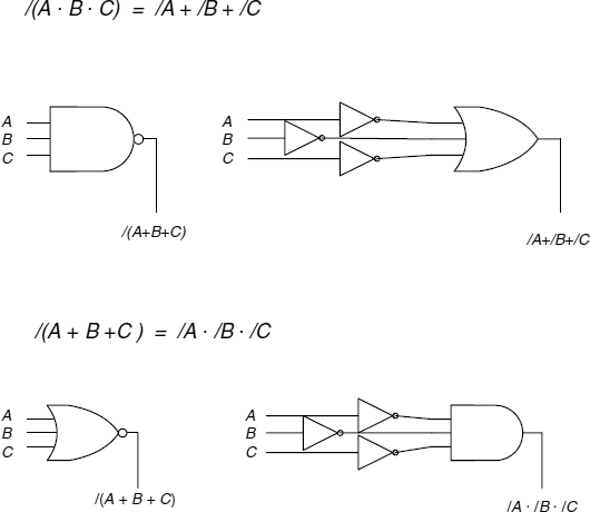
Figure A.9 De Morgan's theorem.
De-Morgan's rules are often used to convert from NAND, /(a · b), to NOR, /a + /b, and from NOR, /(a + b), to NAND, /a · /b.
A.4 EXAMPLES OF APPLYING THE LAWS OF BOOLEAN ALGEBRA
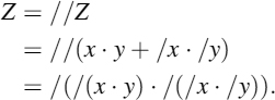
A.4.1 Example: Converting AND-OR to NAND
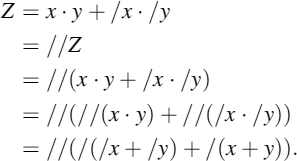
Z = x · y + /x · /y.
Use the De Morgan rule: /(A + B) = /A · /B, where A and B can be any product term. So, in the following example, A is replaced by x · y, and B is replaced by /x · /y:
A.4.2 Example: Converting AND-OR to NOR
Use the De Morgan rule:/(A · B) = /A + /B, where A and B can be any product term. So, in the following example, A is replaced by x · y and B is replaced by /x · /y:
A.4.3 Logical Adjacency Rule
This rule is used in the Karnaugh map method of Boolean algebra minimization and works on the idea that b + /b = 1; so, in the equation
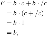
thus eliminating the literal c (in this case).
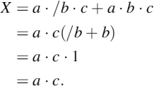
The following example makes use of the Logical adjacency rule:
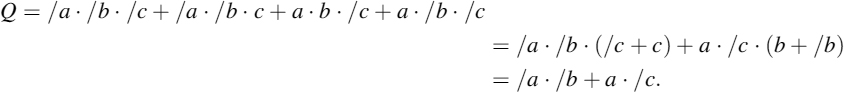
In the next example, the rule is applied twice:
The logical adjacency rule is used in most of the work on synchronous FSM design, and also in establishing correct operation in asynchronous (event) FSM design in Chapter 9.
Both the Aux rule and the logical adjacency rules are often used in the reduction of the flip-flop D, and T equations. That is, a typical equation from a state diagram could be
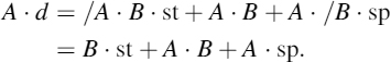
This is obtained from
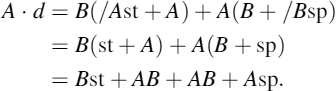
Now:
AB + AB = AB.
Therefore:
A · d = B · st + AB + A · sp.
A.5 SUMMARY
This appendix has looked briefly at the basic laws of Boolean algebra and discussed some of the Boolean techniques used in this book. It provides a reference source for those readers who have not used Boolean algebra for some time. Further information can be found in most books on digital logic.