
Appendix B: Counting and Shifting Circuit Techniques
This appendix contains a number of techniques to help in the development of synchronous binary counters and shift registers. These are used in some of the designs covered in chapters throughout the book.
B.1 BASIC UP AND DOWN SYNCHRONOUS BINARY COUNTER DEVELOPMENT
The development of synchronous pure binary up/down counters can be mechanized to produce a general n-stage pure binary counter. This can then be implemented directly using PLDs/complex PLDs (CPLDs)/FPGA devices. To illustrate how this is achieved, a four-stage down-counter is described below.
Table B.1 shows a down-counter with Q0 the least significant bit. This counter is to be designed as a synchronous counter so all flip-flops will be clocked by the same clock edge. Also, the flip-flops will be T flip-flops. Most CPLDs and FPGAs can support the T flip-flop, either directly or by using D-type flip-flops with an exclusive OR input.
The equation for the T input of each flip flop can be obtained by inspection of Table B.1 and entering a product term for every 0-to-1 and 1-to-0 transition required by each flip flop. For example, from Table B.1 the equation for flip flop q0 · t will be

Each state where the T flip-flop is to change state (0 to 1 or 1 to 0) is entered into the equation.
This can then be written in terms of the Q0Q1Q2Q3 outputs, or simply entered into a Karaugh map as illustrated in Figure B.1. The state map of Figure B.1 can then be used to help to minimize the flip-flop equations.
Since all cells will be filled with ones for the q0 · t equation (every cell whose term appears in the q0 · t equation), then the T input for flip-flop Q0 will be logic 1.
The equation for flip flop q1 · t will be
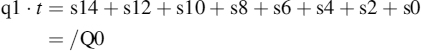
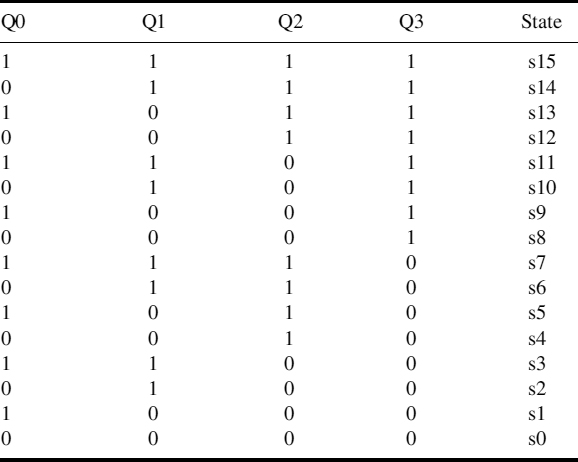
Figure B.1 State map for the counter.
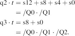
from the state map. An inspection of the state map of Figure B.1 shows that q1 · t must minimise to/q0, since cells s14, s12, s10, s8, s6, s4, s2, and s0 all contain a 1. Following on in this manner, q2 · t and q3 · t can be obtained thus:
The patterns of equations follow in a general manner and can be expressed in the form
Equation (B.1) describes the p terms for a down-counter implemented with T flip-flops. These equations can be directly entered into a Verilog HDL file for each flip-flop.
An up-counter can be realized by replacing all the /q terms in Equation (B.1) with q terms as shown in Equations (B.2) and (B.3):
Or, in general:
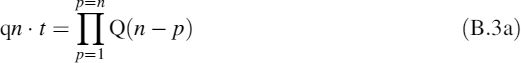
with
For each flip-flop where Π is the product (i.e. AND) of each output term. Note that TFF Q0 has its T input at logic 1. This is not covered in Equation (B.3a).
These equations can be obtained directly from a Karnaugh state map similar to that shown in Figure B.1, but counting in the opposite direction.
B.2 EXAMPLE FOR A 4-BIT SYNCHRONOUS UP-COUNTER USING T-TYPE FLIP-FLOPS
The following example, illustrated in Figure B.2, is a design for a 4-bit up-counting synchronous counter using the techniques described above.
The equations for each T flip flop are
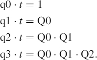
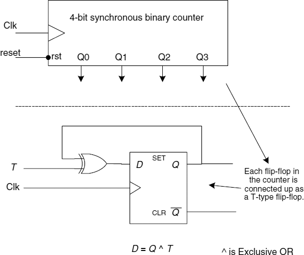
Figure B.2 Block diagram of the 4-bit synchronous binary counter.
This counter can be defined in Verilog HDL as illustrated below in the Verilog source file of Listing B.1.
// Four bit counter design.
// Define the TFF.
module T_FF (q,t,clk,rst);
  output q;
  input t,clk,rst;
  reg q; //q output must be registered - remember?
  always @ (posedge clk or negedge rst)
    if (rst == 0)
      q <=1'b0;
    else
      q <=t^q; // TFF is made up with EX-OR gate.
endmodule

// Now define the counter.
module counter(Q0,Q1,Q2,Q3,clk,rst);

input clk, rst; //clk and rst are inputs.
output Q0,Q1,Q2,Q3; // all q/s outputs.
wire t0,t1,t2,t3; //all t inputs are interconnecting wires.

// need to define instances of each TFF defined earlier.
T_FF ff0(Q0,t0,clk,rst);
T_FF ff1(Q1,t1,clk,rst);
T_FF ff2(Q2,t2,clk,rst);
T_FF ff3(Q3,t3,clk,rst);
// now define the logic connected to each t input.
// we use an assign for this.
assign

t0=1'b1, // this is just following the technique
t1=Q0, // for binary counter design.
t2=Q0&Q1, // will generate AND gates..
t3=Q0&Q1&Q2;
endmodule // end of the module counter.

// Test Bench design to test the circuit under simulation.
module test;
reg clk, rst; // has two inputs which must be registers.
//wire no wires in this part of the design
// since counter is not connected to anything.
counter count(Q0,Q1,Q2,Q3,clk,rst);
initial
  begin
    $dumpfile(“counter4.vcd”); // file waveforms..
    $dumpvars; //dump all values to the file.
      rst=0; // initialise circuit with rst cleared.
      clk=0; //set clk to normally low.
      #10 rst=1; // after 10 time units raise rst to remove reset.
      repeat(17)
      #10 clk = ~clk; //change clk 17 times every 10 time units.
      #20 $finish; //Finish the simulation after 20 time units.
  end // end of test block.
endmodule // end of test module.
Listing B.1 The Verilog HDL file for the counter, with test bench.
The complete Verilog HDL source file with test-bench module for the counter is shown in listing B.1. This contains the T-type flip-flop definition (defined using the behavioural method).
This is followed by the counter definition, which makes use of four instances of the T flip-flops and also uses an assign block to define the logic connections between the flip-flop outputs and the T inputs of each flip-flop. Note: old-style input and output is used outside of the module header.
Following on from this is the test-bench module. This contains an instance of the 4-bit counter followed by the stimulus to test the counter. Note that there are two $ commands to save the timing diagram of Figure B.3 so it can be saved to a Word document (for printout) The command $dumpfile(“counter.vcd”); names the file to be created with the information. The command $dumpvars; simply dumps all variables to the file.
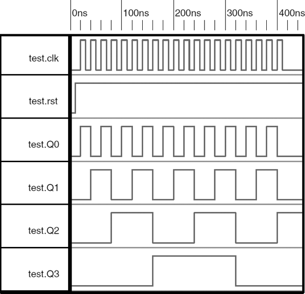
Figure B.3 Simulated 4-bit binary counter.
The file is saved as a ‘metafile’ and is illustrated in Figure B.3. The waveforms of Figure B.3 clearly show the binary counter sequence.
B.3 PARALLEL-LOADING COUNTERS: USING T FLIP-FLOPS
For a parallel loading counter implemented with cheaper PLDs, a synchronous parallel input may be required if there is not an asynchronous preset and clear input to the flip-flops. This can be done by using additional product terms in the qx · t equations.
A general bit slice form with the additional inputs is shown in Equation (B.4) for a TFFx:
The load input is used to load the parallel data synchronously into the flip-flop. In this case, the load input is active high.
In Equation (B.4), the product term ptermx · /load is the normal product term needed for the counter and is true while the load input is not active. The term px · /Qx · load is the parallel input term to set the flip-flop, and the term /px · Qx · load is the term to clear the flip-flop.
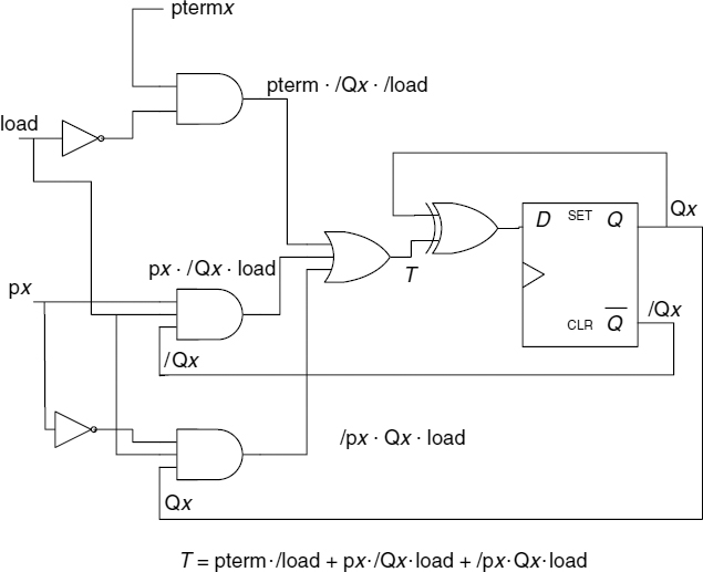
Figure B.4 General structure of a single-flip flop for counting and parallel loading.
Figure B.4 shows a general structure of a single flip-flop. All other flip-flops follow the same general structure. It is assumed here that the active state for the load input is high. Therefore, during counting mode, load would be low (logic 0).
Equations (B.1), (B.2) and (B.4) may be used to produce parallel-loading up/down-counters for many applications, including the address counters for FSMs that control memory.
Thus, it is possible to create not only sequential control of the access of memory, but also random control by way of the parallel inputs.
B.4 USING D FLIP-FLOPS TO BUILD PARALLEL-LOADING COUNTERS WITH CHEAP PROGRAMMABLE LOGIC DEVICES
The D flip-flop can be used in place of the T flip-flop to implement parallel-loading synchronous counters that do not have preset or clear inputs. There are lots of cheaper PLDs that use only D flip-flops and do not have asynchronous preset and clear, so the idea seems attractive.
Consider the circuit of Figure B.5. The bit slice equation for this general model is
where l is the parallel loading input and /l the inverted parallel loading input. This defines the general form for the equations for each flip-flop in the counter chain.
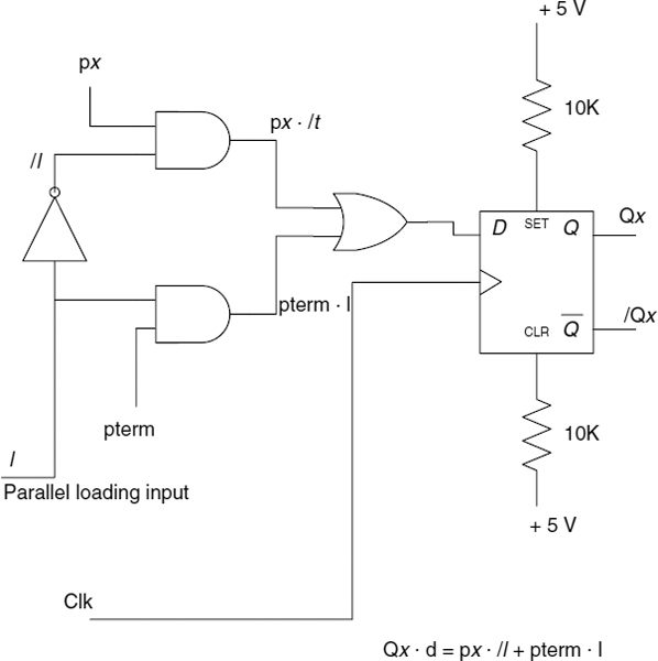
Figure B.5 General bit slice model for of a parallel-loading synchronous counter.
The individual product term pterm here will depend upon the sequence table. There is no simple way to do this; therefore, the method is not as easy to implement as that using T flip-flops.
As an example, consider a simple three-stage synchronous binary up-counter.
B.5 SIMPLE BINARY UP-COUNTER: WITH PARALLEL INPUTS
To illustrate the form in which a physical circuit will take a simple three-stage parallel-loading pure binary counter is illustrated in Figure B.6.
Looking at Figure B.6, the state sequence illustrates the binary sequence. The state map is used to help simplify the pterms (shown here in their simplified form) and, finally, the full equations for the D inputs of each flip-flop.
Note that, compared with the method for designing synchronous parallel-loading up/down-counters using T flip-flops, this arrangement requires the development of each flip-flop pterm. In general, there is no systematic way to do this other than to work out the logic for each flip-flop.
However, one advantage of using D flip-flops is that the count sequence is not restricted to pure binary count sequences (i.e. one could develop unit distance code sequences, for example).
Of course, the counter could be developed from the Verilog HDL behavioural description direct, and this would be the more usual way of doing it. The above method, however, gives an insight into the Boolean equations involved in such counters.
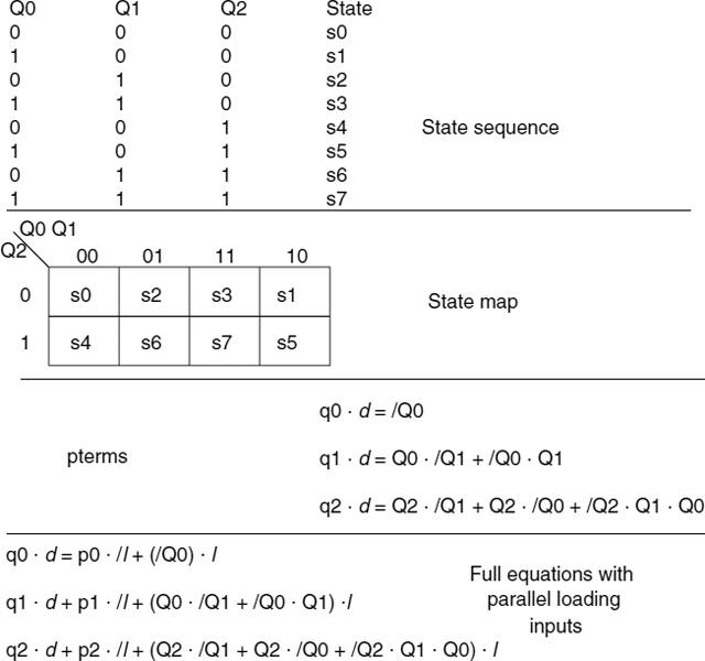
Figure B.6 Illustrating the form of the equations for the three-stage pure binary synchronous counter with parallel inputs.
B.6 CLOCK CIRCUIT TO DRIVE THE COUNTER (AND FINITE-STATE MACHINES)
There are many circuit arrangements for crystal oscillators, but the one shown in Figure B.7 is a common one that is often used. It is included for completeness.
The circuit in Figure B.7 provides overtone suppression via the two capacitors C1 and C2 with values to keep the capacitive reactance small, as indicated in Figure B.7.
B.7 COUNTER DESIGN USING DON'T CARE STATES
In some designs, use can be made of states that do not appear in the count sequence. This can lead to a reduction in the number of gates used in the logic of the counter.
Consider the twisted ring counter, so called because it has each flip-flop connected in the form of a ring, but with a twist in the connection between the last flip-flop and the first. Figure B.8 illustrates the state sequence and a design method using a state map to highlight the don't care states.
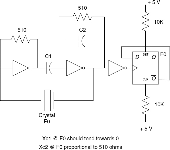
Figure B.7 Typical crystal oscillator circuit.
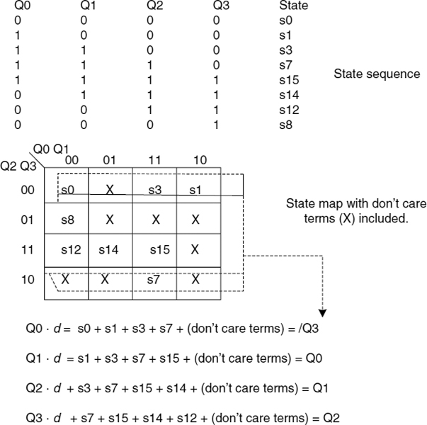
Figure B.8 Twisted ring counter design making use of don't care terms.
The state sequence table in Figure B.8 shows the required sequence for the counter. From this it is apparent that states s2, s4, s5, s6, s9, s10, s11 and s13 are not part of the sequence, so these are made don't care terms (marked as X) in the state map.
From the state sequence table, and state map of Figure B.8, the equations for each flip-flop D input (Qx · d) can be obtained, looking for 0-to-1 and 1-to-1 transitions in each column of the sequence table. The don't care terms are then added to the end of each equation. Finally, the state map is used to obtain the minimized equations.
For example, in equation Q0 · d, states s0, s1, s3 and s7 are combined with don't care terms s2, s4, s5 and s6 to obtain /Q3 (as highlighted by the dotted lines in Figure B.8). The other equations are dealt with in a similar manner.
B.8 SHIFT REGISTERS
A special form of synchronous counter is the shift register. Quite often, a parallel-loading shift register is required (see examples in Chapter 4). The bit slice form for each stage of the parallel-loading shift register is obtained from Equations (B.6a) and (B.6b):
where in this case the active state for the load input ld is low and din is data input.
Note that if serial input is to be zero, make din = 0. The shift register design is using D flip-flops.
These equations could be used to create a four bit parallel loading counter thus:
In Equation (B.7), the first term is the serial data input. In Equations (B.8)–(B.10), the first term denotes that the output of each flip-flop will connect into the input of the next (i.e. a standard shift-register connection). In addition, Equation (B.11) defines the shift clock. This is disabled during parallel loads.
Figure B.9 shows the four-state shift register developed from the Equations (B.7)–(B.11). Note that, in practice, the equations would be converted into Verilog HDL code direct for synthesization. The equations converted into Verilog HDL are:
Q0d = din&ld | po&~ld;
Q1d = Q0&ld | p1&~ld;
Q2d = Q1&ld | p2&~ld;
Q3d = Q2&ld | p3&~ld;
Sft_clk = clk&ld;
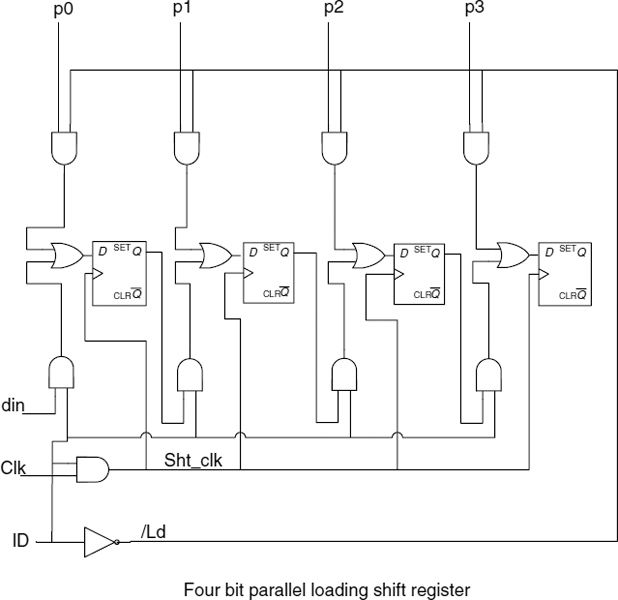
Figure B.9 Four-stage shift register developed from Equations (B.7)–(B.11).
The above shift register, once converted into Verilog HDL code, can then be simulated for correct operation. Figure B.10 shows such a simulation. The Verilog coding is available in the Appendix B folder on the CDROM.
In Chapter 4, the asynchronous serial receiver system made use of a shift register to store the incoming binary data and present them to a data latch. In addition, a divide-by-11 counter was used to keep track of the number of binary bits received and alert the FSM when a complete packet was received (receive shift-register full).
The details and Verilog code for the two modules are now described.
B.9 ASYNCHRONOUS RECEIVER DETAILS OF CHAPTER 4
Figure B.11 (which is Figure 4.21 repeated here for convenience) illustrates the different module blocks needed to make up the complete receiver. Each module in this diagram and its Verilog modules will be described below.
The associated test-bench modules and complete code for the asynchronous receiver are available on the CDROM disk that is supplied with this book. The FSM is described in detail in Section 4.7, with the state diagram Figure 4.22.
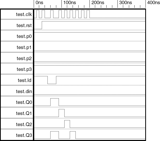
Figure B.10 Simulation of a four-stage shift register with din = 0.
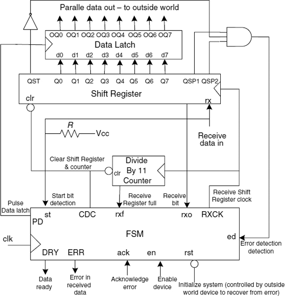
Figure B.11 Asynchronous receiver block diagram from Chapter 4.
B.9.1 The U-Bit Shift Registers for the Asynchronous Receiver Module
This is an 11-bit shift register with a start bit, eight data bits (d0 to d7), and two stop bits (sp1 and sp2).
The incoming data (din) connect to the sp2 flip-flop and are shifted into the sp1 flip-flop. The last flip-flop in the shift register is the start-bit flip-flop, since this is the first data bit into the shift register. This is illustrated in Figure B.12a.
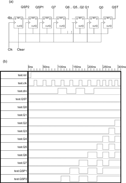
Figure B.12 (a) The shift-registers circuit. (b) Simulation of the shift-register module.
The Verilog HDL code for the shift register is shown in Listing B.2.
// Define DFF
module D_FF(q,d,clk,rst);
  output q;
  input d,clk,rst;
  reg q;
  always @ (posedge clk or negedge rst)
    if (rst==0)
      q<=1'b0;
    else
      q<=d;
endmodule
Listing B.2 Verilog module for the shift register.
Listing B.3 gives the module used to build the shift register.
//---------------------------------------------------------------------
// define shift register
// The shift register clock is rxclk which
// is controlled by the fsm.
// The protocol bits (st, spl, and sp2) are
// shifted into their own FF's.
//---------------------------------------------------------------------

module shifter(rst,clk,din,QST,Q0,Q1,Q2,Q3,Q4,Q5,Q6,Q7,QSP1,QSP2);
  input clk,rst,din;
  output QST,Q0,Q1,Q2,Q3,Q4,Q5,Q6,Q7,QSP1,QSP2;
  wire dst,d0, d1, d2, d3, d4, d5, d6, d7, dsp1, dsp2;

  D_FF_qstd(QST,dst,clk,rst);
  D_FF q0d(Q0,d0,clk,rst);
  D_FF q1d(Q1,d1,clk,rst);
  D_FF q2d(Q2,d2,clk,rst);
  D_FF q3d(Q3,d3,clk,rst);
  D_FF q4d(Q4,d4,clk,rst);
  D_FF q5d(Q5,d5,clk,rst);
  D_FF q6d(Q6,d6,clk,rst);
  D_FF q7d(Q7,d7,clk,rst);
  D_FF qsp1d(QSP1,dsp1,clk,rst);
  D_FF qsp2d(QSP2,dsp2,clk,rst);
  assign
  // note the way that the flip flops have been connected up.
  dst= Q0,
  d0 = Q1,
  d1 = Q2,
  d2 = Q3,
  d3 = Q4,
  d4 = Q5,
  d5 = Q6,
  d6 = Q7,
  d7 = QSP1,
  dsp1 = QSP2,
  dsp2 = din;
endmodule
Listing B.3 Test-bench module for the shift register.
A simulation of the shift register, illustrated in Figure B.12b, indicates that it is working correctly.
A study of the din waveform and the output from the shift register at around the 300 ns point shows that the shift register has received the incoming data, together with the protocol bits.
B.9.2 Divide-by-11 Counter
The counter uses a synchronous pure binary up-counting sequence that counts up to 11 (1101 binary) and then stops. Its output is the RXF signal. This goes high when the eleventh clock pulse is received.
Figure B.13a illustrates the divide-by-11 counter. This is made up of four T-type flip-flops (shown here as D types with exclusive OR gate feedback in the circuit diagram). The four-input NAND gate provides a stop control to inhibit the counter when the count value reaches 11 (Q3Q2Q1Q0 = 1011). The reset input rst is used to reset the counter back to zero.
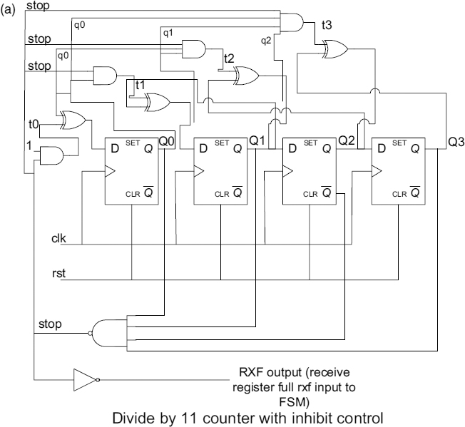
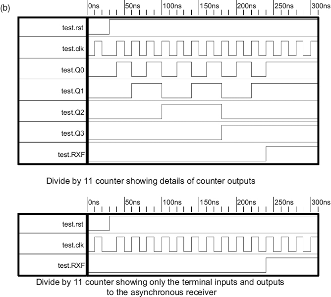
Figure B.13 (a) Schematic circuit diagram of the divide-by-11 counter with inhibit control. (b) The divide-by-11 counter simulation.
The Verilog code for this module is illustrated in Listing B.4 (all variables in lower case).
// define TFF
// Needed for the divide by 11 asynchronous counter.
module T_FF (q,t,clk,rst);
  output q;
  input t,clk,rst;
  reg q;
  always @ (posedge clk or negedge rst)
    if (rst == 0)
      q<=1'b0;
    else
      q<=t^q;
endmodule


// Now define the counter.
module divideby11(Q0,Q1,Q2,Q3,clk,rst,RXF);
input clk, rst; //clk and rst are inputs.
output RXF,Q0,Q1,Q2,Q3; // all q/s outputs.
wire t0,t1,t2,t3,stop; //all t inputs are interconnecting wires.

// need to define instances of each TFF defined earlier.
T_FF ff0(Q0,t0,clk,rst);
T_FF ff1(Q1,t1,clk,rst);
T_FF ff2(Q2,t2,clk,rst);
T_FF ff3(Q3,t3,clk,rst);

// now define the logic connected to each t input.
// use an assign for this.
assign
t0=1'b1&stop, // this is just following the technique
t1=Q0&stop, // for binary counter design.
t2=Q0&Q1&stop, // will generate AND gates..
t3=Q0&Q1&Q2&stop,
stop = ~(Q0&Q1&~Q2&Q3), // to detect 11the clock pulse.
RXF = ~stop;
endmodule // end of the module counter.
Listing B.4 Verilog module for the divide-by-11 counter.
Note that the simulation stops at the eleventh clock pulse due to the NAND gate. This is used to raise the RXF signal via an inverter operation. The RXF (receive register full flag) is used to inform the FSM that the receiver shift register is full. It is cleared by the FSM after transferring the shift register data bits to the octal data latch.
The simulation of this module is illustrated in Figure B.13b.
B.9.3 Complete Simulation of the Asynchronous Receiver Module of Chapter 4
The complete asynchronous receiver with FSM defined in Section 4.7 can now be simulated. The complete Verilog code is contained on the CDROM.
The simulation of the asynchronous receiver is shown in Figure B.14. Here, the only signals visible are those of the complete block, although the secondary state variables are also displayed to show the FSM state sequence. The simulation starts by asserting en high, then the FSM section (signals not seen here) controls the operation of the shift register, divide-by-11 counter, and output data latch.
The data are presented to the user when signal DRY goes high and acknowledged by the user bringing signal ack high. The FSM, in response, lowers DRY (and PD), and the user (optionally) lowers ack to acknowledge the end of the transaction. Prior to loading received data into the data latch its contents are unknown (or the last received).
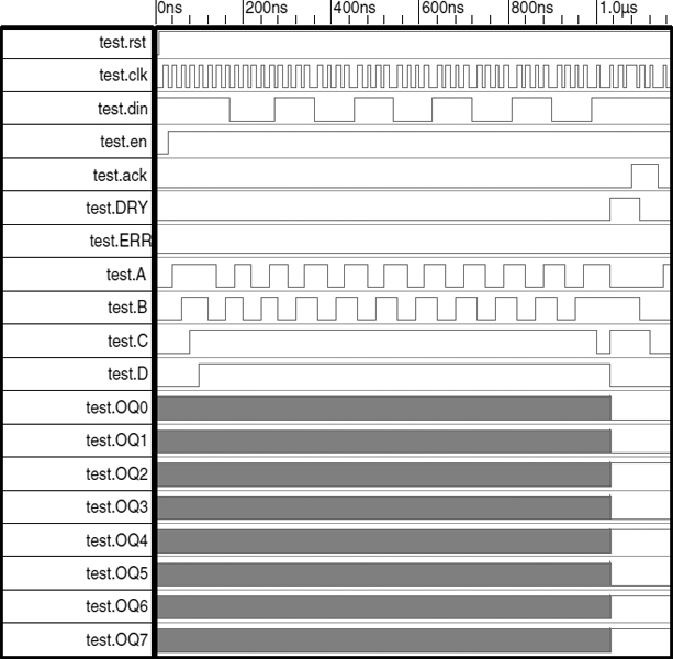
Figure B.14 The complete asynchronous receiver simulation.
B.10 SUMMARY
This appendix has introduced simple ways to develop synchronous up and down pure binary counters, with or without parallel-loading inputs that can be used in a PLD or FPGA device. It has also described how parallel-loading shift registers can be developed and used.
These techniques may be used to develop Verilog HDL modules for use in some of the designs covered in this book. Bit slice equations have been developed to allow counters and shift register circuits to be constructed directly in equation form in Verilog HDL.
Finally, some of these ideas have been used in the development of an asynchronous serial receiver, complete with their Verilog modules.