
Appendix D: Implementing State Machines using Verilog Behavioural Mode
D.1 INTRODUCTION
In Chapters 1–5, state machines have been implemented using the equations obtained from the state diagram. This approach ensures that the logic for the state machine is under complete control of the designer.
However, if the state machine is implemented using behavioural mode, the Verilog compiler will optimize the design.
There is a very close relationship between the state diagram and the behavioural Verilog description that allows a direct translation from the state diagram to the Verilog code.
D.2 THE SINGLE-PULSE/MULTIPLE-PULSE GENERATOR WITH MEMORY FINITE-STATE MACHINE REVISITED
In this system there are two inputs: s to start the system and x to choose either single-pulse or multiple-pulse mode. In single-pulse mode, the L ouput is used to indicate to the user that a single pulse has been generated. In multiple-pulse mode, L is suppressed. Figure D.1 illustrates the state diagram for this system.
Rather than derive the equations directly from the state diagram, a Verilog description can be obtained directly from the state diagram of Figure D.1. This is illustrated in Listing D.1.
// Behavioural State Machine.
module pulsar(s,clk,rst,P,L,ab);
1  input s,clk,rst;
2  output [1:0]ab,P,L;
3  reg[1:0]state, P, L;

4  parameter s0=2′ b00, s1=2′ b01, s2=2′ b11, s3=2′ b10;

   // now define state sequence for FSM (from state diagram).
5  always @ (posedge clk or negedge rst)
6  if (~rst)
7    state <= s0;
8  else
9    case(state)
10     s0: if (s) state <=s1; else state <= s0;
11     s1: state <= s2;
12     s2: if (~x) state <= s3; else state <= s1;
13     s3: if (~s) state <=s0; else state <= s3;
14   endcase

    // now define the outputs @ each state.

15  always@ (state)
16  case(state)
17    s0: begin P=1′ b0; L=1′ b0; end
18    s1: begin P=1′ b1;
19             L= (state==s1) & ~x; //mealy output.
20        end
21  s2: begin L= (state==s2) & ~x; P = 1′ b0; end
22  s3: begin P = 1′ b0; L = (state==s3) & ~x; end
23  endcase
24  assign ab = state;
25  endmodule
Listing D.1 Verilog description of the state diagram.
A comparison between the state diagram of Figure D.1 and the state machine behaviour can be made.
In Listing D.1, lines 5–14 define the state diagram sequence in terms of states and input signals, and lines 15–24 define the outputs in terms of each state. Both of these sets of lines are, of course, happening at the same time (i.e. in parallel).
After declaring the module and its signals in lines 1 and 2, the inputs and outputs are defined.
Outputs are defined in line 2. Note the 2-bit vector [1:0]ab that will be used to show the state of the FSM (Figure D.2). Line 3 defines the state vector [1:0] state used to keep track of the current state of the FSM, as well as the outputs P and L as register type. Line 4 defines the secondary state variables for each state of the state diagram (Figure D.1). Note, these follow the binary values defined for each state in Figure D.1.
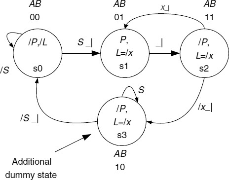
Figure D.1 State diagram for the single pulse with memory FSM.
In line 5, an always statement defines the conditions under which the case statement (lines 9–14) will be used. In line 6, the reset state is defined if rst transition is 1 to 0; otherwise the else will allow the case statement block (lines 10–14) to occur.
The case statement defines the four possible states that the FSM can reside in, and the conditions under which the state transitions occur. The case uses the present state to select one of the four possible next states. Initially, after a reset, state will be s0 (2′ b00) at line 10 and the if statement evaluates input s.
If input s is logic 1, then the next state will be s1; otherwise it will be s0.
On the next posedge of the clock signal the case statement will be activated again. If the current state is s1, then at line 11 the next state will be s2.
Then, on the next posedge of clk, line 12 will ensure that the next state will be either s3 if x = 0, or s1 if it is logic 1. In line 13, the test of input s will decide whether the FSM moves to s0 (s = 0) or remains in s3.
Thus, the state sequence is determined by the case statement and use of the if statement to evaluate input conditions, or just define the next state if no input condition is needed.
The output conditions are defined in a separate case block using outputs for each state as defined in the state diagram. Note that, in line 19, the Mealy output for L in state s1 is defined as
L = (state==s1) &~x;
This ensures that L will be determined by the value of input x(x = 0) and conditional on being in state s1, i.e. L = s1 · /x as defined in the state diagram.
Thus, in this way, ouput L will only be logic 1 if the input x = 0 and the FSM is in s1; otherwise it is suppressed. Output P will be assigned a logic 1 value.
Other case conditions are defined in a similar manner and assigned the output values defined in the state diagram of Figure D.1.
Comparing the behavioural statements from lines 5–14, and lines 15–25 with the state diagram of Figure D.1, it is possible to see a strong relationship between the Verilog description and the state diagram.
Using this approach allows an FSM design to be created without the need to define any hardware logic. It is in fact a 'terminal behaviour and sequence′ for the FSM.
Listing D.2 defines the test-bench module for the system. This follows along the lines of other test-bench modules used elsewhere in the book.
// now define the test bench fixture..
module test;
reg s,clk,rst;
wire [1:0]ab;
wire p, l;
pulsaruut(s,clk,rst,p,l,ab);
initial
  begin
    rst=0;
    clk=0;
    s=0;
    x=0;
    #10 clk=~clk;
    #10 clk=~clk;
    //stays in s0.
    #10 rst=1;
    #10 s=1;
    #10 clk=~clk;
    num;10 clk=~clk;
    // moves to s1.
    #10 clk=~clk;
    #10 clk=~clk;
    // moves to s2.
    #10 clk=~clk;
    #10 clk=~clk;
    // stays in s2.
    #10 s=0;
    #10 clk=~clk;
    #10 clk=~clk;
    // moves back to s0.
    //now make x=1 to produce multiple pulses.
    #10 x=1;
    #10 s=1;
    #10 clk=~clk;
    #10 clk=~clk;
    // move to s1
    #10 clk=~clk;
    #10 clk=~clk;
    // move to s2
    #10 clk=~clk;
    #10 clk=~clk;
    // move to s1 again
    #10 clk=~clk;
    #10 clk=~clk;
    // and back to s1
    #10 clk=~clk;
    #10 clk=~clk;
    // s2 again
    #10 clk=~clk;
    #10 clk=~clk;
    #10 x=0; //prepare to stop multiple pulse mode.
    #10 clk=~clk;
    #10 clk=~clk;
    // to s3.
    #10 clk=~clk;
    #10 clk=~clk;
    #10 s=0;
    #10 clk=~clk;
    #10 clk=~clk;
    // back to s0.
    #10 $stop;
  end
endmodule
Listing D.2 The test-bench module.
Figure D.2 illustrates the simulation waveforms for the design. Note the vector ab defining the state of the FSM at each clock transition. Compare this with the state diagram of Figure D.1.
You should follow the waveform sequence to determine the paths taken through the state diagram sequence. Both modes are tested and seen to work:
with x = 0, the FSM is seen to produce a single output pulse;
with x = 1, the FSM produces a series of output pulses as it moves between si and s2, finally returning to state s0 when x = 0.
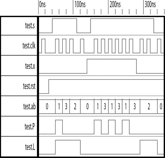
Figure D.2 Simulation of the FSM using Listings D.1 and D.2.
D.3 THE MEMORY TESTER FINITE-STATE MACHINE IN SECTION 5.6
This example can be coded directly in Verilog as a behavioural description using the state diagram of Figure 5.15. The listing is illustrated in Listing D.3.
module
memory tester state machine(clk,rst,st,fab,full,RC,P,CS,RD,WR,OK, ERROR,abc);
   input clk,rst,st,fab,full;
   output[3:0]abc,RC,P,CS,RD,WR,OK,ERROR;

   reg[3:0]state, RC,P,CS,RD,WR,OK,ERROR;
// assign secondary state variable values (as used in Figure 5.15)
   parameter s0=4′ b0000, s1=4′ b1000, s2=4′ b1010, s3=4′ b0010,
             s4=4′ b0110, s5=4′ b1110, s6=4′ b1100, s7=4′ b1101,
             s8=4′ b1001, s9=4′ b1011, s10=4′ b0100;

// the state machine sequence..

always @ (posedge clk or negedge rst)
   if (~rst)
     state=s0;
   else
   case(state)
     s0: if(st) state <=s1; else state <=s0;
     s1: state <= s2;
     s2: state <= s3;
     s3: state <= s4;
     s4: state <= s5;
     s5: state <= s6;
     s6: if(fab) state <= s7; else state <= s10;
     s7: state <= s8;
     s8: if (full) state <= s9; else state <= s1;
     s9: state <= s9;
     s10: state <= s10;
   endcase

// the outputs for each state.

always@ (state)
   begin
   {RC,P,CS,RD,WR,OK,ERROR} = 7′ b0011100;
   case(state)
     s0: begin assign RC=1′ b0;
           P=0;
           CS=1;
           RD=1;
           WR=1;
           OK=0;
           ERROR=0;
     end
    s1: begin assign RC=1′ b1;
           CS=1′ b0;
           P=0; end
    s2: begin WR=1′ b0; end
    s3: begin C S=1′ b0;
           WR=1′ b1; end
    s4: begin end
    s5: begin RD=1′ b0;end
    s6: begin end
    s7: begin RD=1′ b1; end
    s8: begin CS = 1′ b1;
           P=1′ b1; end
    s9: begin OK=1′ b1;
           P=0; end
    s10: begin ERROR=1′ b1; end
endcase

end
assign abc = state;
endmodule
module test;
   reg st,clk,rst,fab,full;
   wire[ 3:0]abc;

   memory tester state machine
uut(clk,rst,st,fab,full,RC,P,CS,RD,WR,OK,ERROR,abc);

   initial
     begin
       rst=0;
       clk=0;
       st=0;
       fab=0;
       full=0;
       #10 rst=1;
       #10 st=1;
       #10 repeat(14)
          #10 clk=~clk;
       #10 rst=0;
       #10 rst=1;
       #10 repeat(10)
       #10 clk=~clk;
       #10 fab=1;
       #10 repeat(16)
       #10 clk=~clk;
       #10 clk=~clk;
       //#10 rst=0;
       //#10 rst=1;
       #10 full=1;
       #10 repeat(20)
       #10 clk=~clk;
       #10 $finish;
     end
endmodule
Listing D.3 Behavioural description of memory tester from state diagram of Figure 5.15.
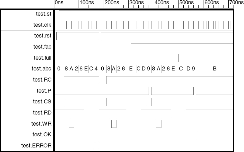
Figure D.3 Simulation of the memory tester FSM of Listing D.3.
The simulation is shown in Figure D.3.
The abc vector illustrates the FSM states in terms of the secondary state variables allocated in the state diagram of Figure 5.15. These were assigned to provide a unit distance code, and the numbers shown in the simulation in Figure D.3 are the hexadecimal values.
The FSM is seen to move around the state diagram from state s0(0) through s1(8), s2(A), s3(2), s4(6), s5(E), s6(C), then s10(4) the error state. The FSM is then reset back to state s0 and recycles around the state diagram to s8(9) and on to s9(B) the OK state.
The write cycle (8, A, 2) is followed by the read cycle (E, C), and again in (8, A, 2, 6, E, C, D).
D.4 SUMMARY
The use of a behavioural description has the advantage of using the information in the state diagram directly. It can be seen that there is a one-to-one correspondence between the state diagram structure and the Verilog structure, and this shows how the state diagram method can allow a realization of the design directly (via the behavioural method) or via the Boolean equations.
Both methods, owing to their formal descriptions, are suitable for computer implementation. This has been exploited in a number of programs developed at Northumbria University by postgraduate students.