
2
Using State Diagrams to Control External Hardware Subsystems
2.1 INTRODUCTION
In real-world problems there is often a need to use external subsystems, such as hardware timers/counters, analogue-to-digital converters (ADCs), memory devices, and handshake signals to communicate with external devices.
This chapter looks at how a state diagram (and, hence, an FSM) can be used to control such devices. This opens up a much wider range of activities for the FSM and can lead to solutions in hardware that can be implemented in a relatively short time.
In later chapters, the ideas explored in this chapter will be used to develop some interesting real-world systems.
2.2 LEARNING MATERIAL
One of the most common requirements in an FSM is the need to wait in a state for some predefined period. For example, a need to turn on an outside world output for a certain period of time, then turn it off again. This could be done by just allocating a number of consecutive states with the required output held high, but this would be very wasteful of states (and the corresponding flip-flops needed to implement the FSM) for all but very short delays. The best way of dealing with this kind of requirement is to use an external timer unit that can be controlled by the FSM.
A typical timer unit might look something like the illustration in Figure 2.1.
The timer unit has two inputs, the clock input clk and the start timer input ts, and a single output TO. From the timing diagram (Figure 2.1) for this timer unit, the timer output TO will go high when the timer start input ts makes a 0-to-1 transition. The output TO will remain high until the time period has elapsed, after which it will go low.

In Figure 2.2, TS, an output from the FSM, is used to start the timer prior to the time-out state. Then, on the next clock pulse the FSM moves into the time-out state. In the time-out state, the TS signal is returned low and the timer output signal ‘to’ is monitored by the FSM, which is looking for this ‘to’ signal going low, signalling the end of the timer period. At this point, the FSM will leave the time-out state.
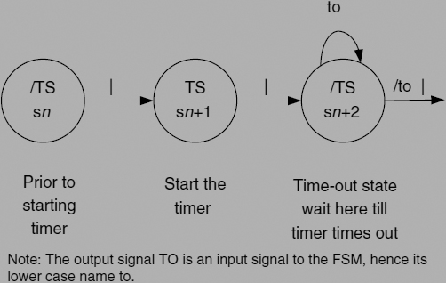
Figure 2.2 State sequence to control the timing module.
Note that the FSM will wait in state sn + 2 until the signal ‘to’ goes low. Therefore, the time spent in state sn + 2 will be dictated by the timer unit.
Also note here that the timer output signal ‘to’ is in lower case now, since it is an input to the FSM, whereas the timer input signal TS is uppercase, since it is an output from the FSM.
Now please turn to Frame 2.2.
An example of how the timer unit could be used now follows.
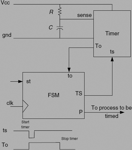
Figure 2.3 Block diagram showing how to use the timing module.
In Figure 2.3, the FSM is controlling a timer unit. This timer unit happens to be a little different to the one seen in Frame 2.1 in that it does not have a clock input. It is in fact a timer based around an RC charging circuit (a practical device would be the 555 timer units that are readily available). This does not alter things in any way as far as the FSM is concerned. Note that the actual time delay would be given by
To = 1.1 × C × R.
if Timer is a 555 timer chip.
The start input St starts the FSM from state s0. The idea here is to turn on the process P for a period of time (dictated by the RC time constant of the timer unit), then turn it back off again.
| Task | Produce the state diagram to do this. Then go to Frame 2.3 for a solution. |
The state diagram to implement the arrangement shown in Figure 2.3 is shown in Figure 2.4.
The process P is turned on in state s1, since the timer is started in this state, before the FSM moves into the time-out state s2. The FSM will remain in state s2 monitoring the timer output signal ‘to’ until the timer has timed out, and then move to state s3 to stop the process P.
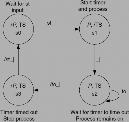
Figure 2.4 State diagram using the Timer module.
Using this arrangement allows the FSM to be held in the wait state for any length of time, depending only on the value of the RC time constant.
Go to Frame 2.4.
Having seen how to control an outside world device like a timer, the next stage is to see how other outside world devices can be controlled. This is really what FSMs are all about, controlling outside world devices.
Now look at how an FSM can be used to control
- an ADC;
- a memory device.
Controlling an ADC
ADCs are used to convert analogue data into digital form. They are needed to allow digital computers to be able to process data from the real world (which is essentially analogue in nature). Most systems that use an ADC will be controlled from a microprocessor (or microcomputer). However, it is often the case that a system (or part of a system) will be implemented using a customized chip design, a programmable logic device (PLD), or even a field programmable logic array (FPGA). Consider the ADC shown in Figure 2.5.
This ADC has (as is usually the case) a Start Conversion input SC and an End Of Conversion output eoc.

Figure 2.5 Controlling an ADC from a state diagram.
The analogue input and digital outputs are connected to the external circuit and are not part of the FSM, since they form the data flow part of the system. The FSM is used to control the system components (the ADC in this case).
The segment of state diagram shows how the ADC is controlled by an FSM.
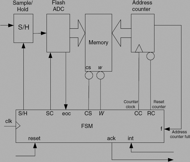
Figure 2.6 Block diagram for a small DAS.
The FSM starts the ADC conversion in state si and waits for the eoc1 signal from the ADC to say that a digital value is available at the outputs of the ADC. At this point the FSM will move into state s2. Here, it will wait for eoc to return low before moving on to the next state.
Now consider the small data acquisition system (DAS) shown in Figure 2.6.
In this system there is an ADC and a number of other outside world devices.
Go to Frame 2.5.
This particular example is a bit more complicated than the examples looked at so far; however, it can be separated out into more manageable parts, as will be revealed.
The diagram shown in Figure 2.6 uses the FSM to control a sample-and-hold (S/H) amplifier, ADC, a random access memory (RAM) device, and a simple binary counter.
All these outside world components allow the FSM to be able to
- sample a.c. analogue data from the outside world;
- store the data in RAM.
These could be under the control of a remote end device (which could be a microcomputer).
Before attempting to produce a state diagram for this FSM, discussion is required on how an FSM can control the RAM and counter.
Consider Figure 2.7, which shows a memory device controlled by an FSM.
The memory device is written to/read from in sn+3 (on the rising edge of the read or write signal). Note that the memory device has a collection of address input lines (commonly called the address bus) and a set of data lines called the data bus. If the memory is read, only the data bus lines will be outputs. If the memory is a RAM, then the data bus lines will be bidirectional. This means that the /R and /W control signals can be used to condition the data bus lines to be either inputs (when /W is used) or outputs (when /R is used). In addition, there is a chip select input to select the memory chip.
Further information on memory device timing
Figure 2.8 shows all the waveforms associated with a memory device.
The address bus selects a particular memory location at time T1 (the address bus lines changing just after the T1 starts). This causes the chip select CE signal to become active (low) at time T2 (allowing for propagation delays through the logic).
At time T3, the write signal W is activated (active low) and, as a result of this action, the memory chip data bus is taken out of its normal tri-state condition so it can accept input data.
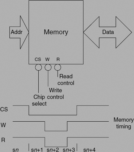
Figure 2.7 Control of a memory device.
At time T4 (after a suitable time has been allowed for the memory to settle) the write W signal is taken high, then the chip select signal CE will be taken high to deselect the memory chip. It is during this transition (0 to 1) of the W signal that the data are written into the memory chip. Note that in some memory chips the CE and W signals appear to go high in T4 at the same time. The microprocessor will hold CE low long enough to allow the W signal to write the data into the memory device. This is usually because the propagation delay is longer in the CE path due to additional address decoding logic.
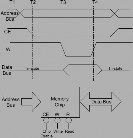
Figure 2.8 Timing of the control of a memory device.
In a system controlled by an FSM, this can be done in the waveform diagram sequence, as shown earlier in this frame in Figure 2.7. However, an alternative arrangement could be to cause the CE signal to be delayed within the memory chip. This would be possible if the memory was being implemented in an HDL to be contained in an FPGA, perhaps also containing the FSM.
The main thing here is to ensure that the data can be written into the RAM before it is deselected.
Note: the signals CE and W need to be controlled by the FSM whenever the memory is to be written to or read from.
Note that if W is replaced by R then the memory cycle is a read memory cycle in which data stored in the memory chip will be output from the chip.
The read operation follows the same basic sequence as the write signal, and the arguments discussed earlier about delaying the chip select also apply.
Now go to Frame 2.6 to see how the memory chip can be controlled from an FSM.
To access the memory device, the chip select line must be asserted (this means that the chip select line must be active, in this case active is logic 0). Then, write data into the RAM device by lowering the write signal line. A little later, raise the write line to logic 1 to write the data into the RAM device.
To read the contents of the RAM, first select the chip select line by making it go low, then a little time later set the read line low.
In most cases, ‘chip select and read’ or ‘chip select and write’ control lines can be raised high (to disassert them) at the same time. It is usually at this point in the cycle that the memory device is read or written; but, if there is a doubt about chip select remaining low long enough for the write or read operation to take place, then it is best to raise write or read first before raising the chip select signal.
In practice, the data bus will remain active for a few nanoseconds (typically 10 ns) in order for the data to be written or read by memory in memory controlled by a microprocessor, but in an FSM-controlled system the design engineer should ensure that this occurs either by adding another state to the state machine or by creating a delay on the chip select signal in the memory device.
The segment of timing diagrams of Figure 2.7 in Frame 2.5 illustrates this process.
When reading from and writing to memory devices, the process of reading and writing is implied to be from the point of view of the controlling device. The controlling device in a microprocessor system is the microprocessor. In our case, the controlling device is the FSM.
| Task | Try producing a segment of state diagram to control the memory device for writing. |
Now go to Frame 2.7 to find out whether it is correct.
The segment of state diagram to control the memory illustrated in Frames 2.5 and 2.6 is illustrated in Figure 2.9.
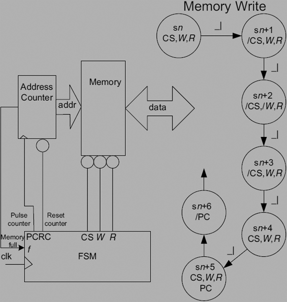
Figure 2.9 Using an FSM to control the writing of data to a memory device.
In state sn, all controls are disasserted. In sn + 1 the chip select line CS is active; then, in state sn + 2, the write control line W is active. In state sn + 3, W is deactivated to write the data into the memory, and it is at this point that the data are written into the memory device. Finally, in state sn + 4, the chip select CS is raised to deselect the memory device.
To read or write to a memory device, the data transaction will occur in the memory element currently accessed by the address bus. To access another memory element, another address needs to be selected; this is done by the address counter. This is what the counter in Figure 2.6 (and in Figure 2.9) is being used for. In this case, each memory location is selected in sequence by incrementing the binary counter after accessing each memory location.
Note that in state sn + 5 the signal PC is set high. This increments the counter, thereby incrementing the address to point to the next consecutive memory location.
The counter can be reset to zero by sending the signal RC to logic 0. It can be incremented by the FSM with a pulse to the PC signal. In this way, each memory location of the memory can be accessed sequentially. Note that the address counter is incremented after disasserting the memory chip. This is because the address on the memory chip should not be changed while it is selected.
Go to Frame 2.8.
| Task | Having seen how the individual outside world devices are controlled in Figure 2.6, try to produce a state diagram to implement the FSM used to control the system. |
The FSM is to wait in state s0 until it receives an interrupt signal from the remote end device over the int signal line. When this occurs, the FSM is to
- obtain a sample of data;
- perform an analogue-to-digital conversion;
- store the converted value into the memory device;
- increment the counter to point to the next available memory location.
The FSM should keep on doing this until the memory device is full. The FSM will know this when the f input (from the counter) goes high.
At this point, the FSM is to send an acknowledge signal to the remote end device using the ACK signal line; then, once the signal line int is low (remember, it was asserted high at the beginning of the sequence), it is to return to state s0 ready for another cycle.
When completed, go to Frame 2.9.
The complete state diagram is illustrated in Figure 2.10. Your state diagram may not look quite like this one, as there is more than one way of drawing a state diagram and there is no ‘one’ correct solution. However, the diagram in Figure 2.10 is very concise.
The first thing to note is that the reset line RC used to hold the memory address counter reset is held active (asserted) in state s0. Thereafter, it is held in its disasserted state (i.e. RC = 1).
Not all states show this, but the sequential nature of the state diagram implies it.
When the int input is asserted, the FSM moves into state s1, removing the reset from the address counter and simultaneously asserting the sample-and-hold amplifier S/H = 1.
On the next clock pulse, the FSM moves to state s2, where (with the S/H still set) the start conversion signal of the ADC is asserted SC = 1. At this point, the FSM waits for the end of conversion signal eoc = 1; then, on the next clock pulse, it moves to state s3, where the S/H signal is disasserted (S/H = 0), since the ADC has converted the analogue data into digital form. While in state s3 the chip select in asserted (CS = 0) and the FSM waits in state s3 for eoc to be returned low. When this happens, on the next clock pulse the FSM moves to s4, where the memory device write signal line W is asserted low to set up the memory data bus lines as inputs. This allows the ADC digital output value to be input to the memory.
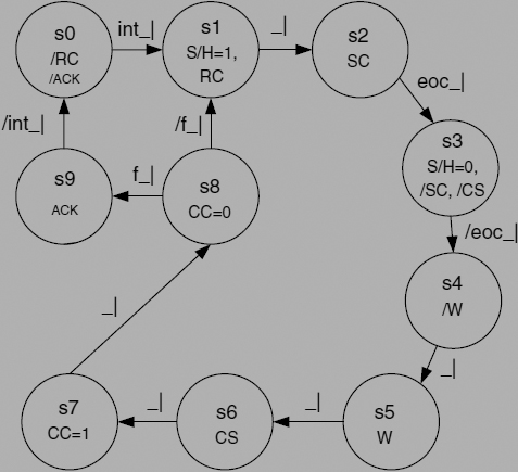
Figure 2.10 State diagram for the DAS.
The next clock pulse will move the FSM into state s5, where W is disasserted high, thereby writing the ADC value into the memory chip.
The FSM now moves into state s6 on the next clock pulse to deselect the memory (CS = 1).
Go to Frame 2.10.
At this stage in the FSM cycle, the FSM is in state s6.
The state machine will now move to state s7, where CC will be asserted high. On the next clock pulse, the state machine moves to s8, where CC will go low. The 0-to-1 transition on this signal line, caused by the FSM moving from state s6 to s7, will cause the address counter to increment. Note that, in state s6, the CS and W signals are now both high (disasserted).
In state s8 the FSM can move, either to state s1, if the signal f is disasserted low (hence repeating the sequence s1 to s8), or, if signal f is asserted, the FSM can move from s8 into s9.
The signal f is used to indicate whether the address counter has reached the end of the memory. If it has not reached the end of the memory (f = 0) then another cycle is started, otherwise the FSM moves into state s9 where the ACK signal will be asserted high to let the external device know that the FSM has completed its tasks. The FSM will wait for the signal int going low.
By waiting for int to go low, the FSM will be ready for the next low to high transition on int to start the next cycle of operations. Note that the external device will need to lower the int signal to complete the handshake. On seeing int go low, the FSM lowers the ACK signal to complete the handshake.
The forgoing example is quite a complex one and shows how an FSM can be used to control a complex sequence to control a number of outside world devices.
As seen from this example, the development of a state diagram is largely an intuitive process. However, by applying the techniques discussed in this book the reader can become experienced in developing their own state diagrams to control external devices.
Some of the ideas put forward in this text are as follows:
- ANDing clock and other input signals to an outside world output to form Mealy outputs (Frame 1.16, Figure 1.18);
- using dummy states to obtain unit distance coding (Frames 1.12 and 1.13);
- using an external timer to provide a wait state (Frame 2.1);
- using the FSM to control outside world devices like ADC (Frame 2.4) and memory devices (Frame 2.5).
The steps necessary to get from a state diagram to a functional circuit are very mechanical and will be discussed in Chapter 3.
However, before looking at Chapter 3, there are a number of other techniques that need to be considered.
Move on to Frame 2.11.
Consider the block diagram of an FSM in Figure 2.11.
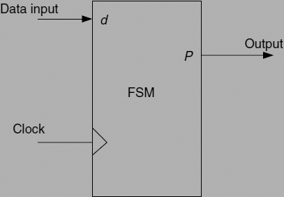
Figure 2.11 Block diagram for the data-input FSM.
In this particular FSM, a single clock pulse is required at the output P whenever the d input is asserted high twice.
| Task | Try producing a state diagram for this one, then turn to Frame 2.12 to see a solution. |
The block diagram of Frame 2.11 is repeated in Figure 2.12.
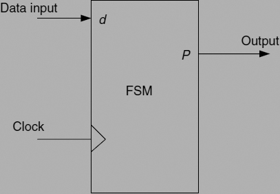
Figure 2.12 Block diagram for the data-input FSM.
The point to note here is to monitor the input for change. This implies the need to monitor d for two assertions.
The monitoring of d is very important in this example, since the FSM must determine when d has been asserted twice. To do this, monitor d going high, then monitor d going low (at this point, d has gone high then low once). Continue to monitor d going high again, followed by monitoring d going low (at this point, d has gone high then low twice).
The state diagram is shown in Figure 2.13.
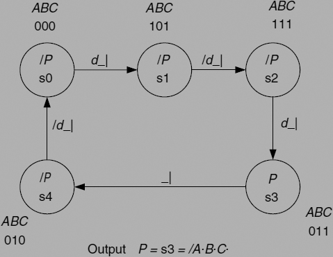
Figure 2.13 State diagram to detect two 1-to-0 transitions of d input.
In this state diagram, the FSM monitors the d input going high, then low (s0 and s1), then monitors d going high again (s2 and s3). In state s3, the FSM knows that d has been asserted twice, so the output P is allowed to become asserted high. The FSM moves out of state s3 on the next clock pulse and waits in state s4 for the d input to go low before moving back into state s0. So, inputs with multiple assertions must be monitored by the FSM.
Note that in Figure 2.13 the state assignments between s0 and s1 and between s4 and s0 are not unit distance. You might like to try to obtain a unit distance coding for the state diagram.
A possible solution is as follows. A dummy state needs to be added to the state diagram, a possible place would be between s3 and s4 (call it s5). Then, the following unit distance state assignment could be applied: s0 = 000, s1 = 100, s2 = 110, s3 = 111, s5(dummy) = 011, s4 = 001.
Go to Frame 2.13.
Frame 2.13 A sequence detector
Consider the example shown in Figure 2.14.
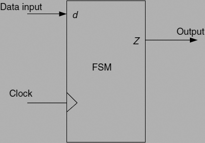
Figure 2.14 Block diagram for the 110 sequence detector.
This detector has the timing diagram shown in Figure 2.15.
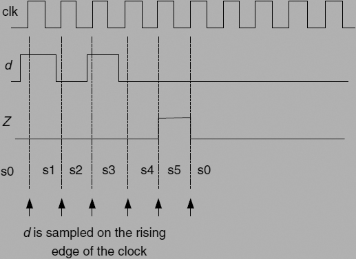
Figure 2.15 Possible timing diagram for the 110 sequence detector.
Note, d is sampled on the 0-to-1 transition of the clock (shown by the arrows in n Figure 2.15).
The FSM changes state on the 0-to-1 clock transition also. The timing diagram illustrates how the FSM is to do this.
In the timing diagram of Figure 2.15, d follows a 110 sequence. In practice, of course, one needs to produce an FSM that can identify the 110 sequence from all other possible sequences. Only the 110 sequence, however, should produce a Z output pulse.
| Task | Assume that the d input is a succession of pulses, i.e. 1 → 0 → 1 → 0 is two D pulses. Try producing a state diagram for such an FSM. |
| Hint | Produce the state diagram for detecting the required 110 sequence first, then add to this state diagram the necessary transitions to cover all other sequences. |
Go to Frame 2.14 to see the solution.
The state diagram for the 110 sequence detector is shown in Figure 2.16.
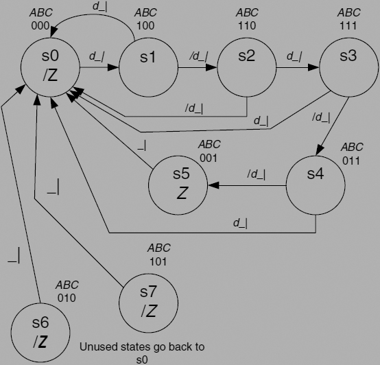
Figure 2.16 State diagram for the 110 sequence detector.
The sequence s0, s1, s2, s3, s4 and s5 detects the 110 sequence (note the assumption that the d input is a succession of pulses).
The loop back terms catering for all other sequences are to return the FSM back to state s0 in order to keep on detecting the 110 sequence. The timing diagram of Figure 2.15 should help to explain the different transitions.
Note that the state diagram above uses six states. The secondary state variables allow eight states; therefore, there are two states that are not used. What would happen if the FSM were to fall into one of these two unused states ? The answer to this question is that the FSM would not be able to get out of the unused state and the FSM would ‘hang’.
To avoid this calamity, it is common to direct all unused states back to state s0 so that the FSM can recover from this misadventure. This is shown in Figure 2.16, where states s6 and s7 are directed back to state s0 on the next clock pulse.
Note that when using D-type flip-flops to implement the state machine, getting into an unused state will automatically cause the FSM to reset to state s0; therefore, it is not necessary to connect unused states back to s0 in this case. More on this later.
2.3 SUMMARY
This chapter has dealt with the way in which FSMs can be used to control external hardware in a digital system. Later chapters will illustrate how these and other external devices can be controlled by an FSM. One of the implications from this work is that many of the applications normally developed using microcontrollers can be implemented using FSMs and hardware logic. The block diagram and state diagram approach seen in Chapters 1 and 2 can be used, in conjunction with modern HDLs to make this possible. The advantage, in some cases, will be a design that uses less logic than a similar design using a microcontroller. You will see this possibility later on when you have read later chapters.
For now, the next stage in our work is to see how a state diagram can be used to create a logic circuit to realize the design. This work is covered in Chapter 3.
1 Note that some ADCs have a busy signal instead of the eoc. These ADCs raise the busy signal when SC is asserted, lowering it when the conversion is complete.