
3
The Digital Sensor
The sensor is naturally the key element of the digital photographic camera. Though the first solid detectors were metal-oxide semiconductor (MOS) photodiodes, at the end of the 1960s, it is the charge-coupled devices (CCD) technology, discovered in 19691, which has for many years constituted most of the sensors of photo cameras2. Since the year 2000, the complementary metal-oxide semiconductor (CMOS) transistor technology developed in 1980s, has concurrently spread for reasons we will see later, it is rapidly becoming the standard. Today, other materials are being developed to improve the performance of the sensor, especially quantum dots in graphene nanostructures [JOH 15, LIU 14] or colloidal crystals [CLI 08], which could eventually deliver exceptional performances regarding both the efficiency of photon/electron conversions (greater than 1) and detection speed. We will quickly address these sensors in the chapter on color, in section 5.4.1.2.
The efforts to develop sensors have taken several directions that all result in a complexification of the manufacturing processes:
- – a densification of the photosites3;
- – an increased performance: sensitivity, linearity, immunity to noises;
- – an integration of processes at the sensor to improve the signal and unburden the central processor of systematic operations.
It is according to these three axes that our presentation will be developed.
3.1. Sensor size
The race for miniaturization has been driven with two objectives:
- 1) to reduce the size of the sensor, in particular for mobile phones (today, the aim is a sensor with a side of a few millimeters, maintaining at the same time a high number of pixels) (see Figure 3.1);
- 2) to increase the resolution for a fixed image field size (the format 24 × 36 mm being used as commercial reference).
Consequently, we should examine the various aspects of the physical size of the sensor, a very important point in image quality as for the whole optics and electronics architecture of the camera.
3.1.1. Sensor aspect ratio
The aspect ratio is the ratio between the large and the small side of the image. Two different trends are found in competition in the early days of digital photography:
- – the ratio 3/2 = 1.5 which is the most popular format in film photography (the 24 × 36 of the 135 film);
- – the 4/3 = 1.33 report that corresponds to super video graphics array (SVGA) video screens and allowed a direct full-field display.
These two aspects have been chosen today for the majority of commercialized sensors. Cameras still offer images with a broad variety of aspect ratios (of which, for example, the 16/9, originating from cinema, which predominates today in video). Nonetheless, when the aspect ratio of the pictures is not identical to that of the sensor, the image is obtained by trimming the original image and discarding pixels when storing, which can be achieved a posteriori in a similar fashion.
It should be noted that the square format which has a certain success in photography circles, is not found in digital sensors, the medium formats that make extensive use of them have nowadays opted for rectangular sensors. Yet, it is the most appropriate regular format to exploit the properties of an objective rotationally symmetric by nature. However, the square format is poorly adapted to a reflex assembly because the mirror requires a large amount of space to move. The 4/3 format, closer to the ideal square, is a step toward the optimization of the couple (optics vs sensor) that reveals its full meaning in non-SLR assemblies (compact and hybrid).
Finally, some cameras now offer a stereoscopic capture (through a single lens) and to this end reserve the right-hand half of the sensors for the right picture and the left-hand half for the left image (separated by their paths in the objective). The format of the resulting image is then half that of the sensor. The same occurs for some sensors that use pairs of neighboring pixels to capture a high-density signal by separating the strong signals on even photosites from the weak signals on odd photosites.
3.1.2. Sensor dimensions
The integration of sensors with microelectronics technologies has met, in the early days of the digital camera, the limitations of masking techniques that hardly covered wide angles with a single exposure. This has very much promoted the development of small-size sensors. Gradually, by overcoming these constraints, sensors with larger dimensions have emerged (see Figure 3.1).
We have highlighted that the Full Frame format (24 × 36 mm) is the commercial reference. Originating from film photography, the 24 mm × 36 mm format is also called 35 mm (due to the width of the film) or designated by the code 135. It was not achievable in the early days of photography and manufacturers have used conventional but smaller photographic formats, such as the advanced photo system (APS) or new original formats (the CX, the Micro 4/3). Others, especially in the area of compacts and of telephones, have sought inspiration from the world of electronics for denominating the sensors developed by following the practices being used for video tubes: a sensor is qualified by the inch fraction occupied by 1.5 × the diagonal of the sensor (the factor 1.5 comes from the optical mount that surrounds a video tube but has no relationship with photo editing itself).
Thus, a 7.5 mm × 5.6 mm sensor will be referred to as 1/1.7″ because its diagonal is about 10 mm and 10 × 1.7 × 1.5 ~ 25.4 mm. This denomination is only approximated and allows the definition of classes of sensors (see Figure 3.1), rather than a fine identification.

Figure 3.1. A few sensor formats available in 2015. The reference in photography is the 24 × 36 mm format, referred to as full frame in this diagram. A very large number of sensors are smaller today than the sensor of the iPhone4 (3.39 mm × 4.54 mm), in particular on mobile phones. They are not represented here. Intermediate sizes, shown here along with their technical denomination, either designed by photography (APS, 4/3, CX), or sometimes video manufacturers/companies (in inches fractions), do not always follow a standard size (for example, the APS-C can vary a few percent depending on the manufacturer). Medium format sensors, larger than full frames, (Pentax, Mamiya or Hasselblad here) are rare and expensive
Despite the success of smaller sizes, the 24 mm × 36 mm format has remained the holy grail of photographers because of the long history that is associated with it and the range of objectives and accessories available.
“Full-frame” cameras are now fairly widespread among high-range SLRs. They are optically compatible with the objectives designed for analog cameras (same covered angle, aberrations also compensated), but the features of these objectives are often unsuited for modern developments (stabilization, focus, zoom, etc.). They are mainly in demand because of the quality of their image, this being in theory, directly dependent on the size of the sensor as it will be discussed in Chapter 7.
Full-frame sensors have also recently emerged in hybrid cameras that are yet sought for their compactness and their lightness.
Most quality cameras that are not full frame have either 34 mm diagonal APS4 or 22 mm diagonal Micro 4/3 formats. Compacts have formats ranging from the CX to the 1/2.3″, while mobile phones are reduced down to millimeter sizes.
However, manufacturers of “medium format” cameras (see Chapter 1) have gradually developed sensors with larger surface areas, first by juxtaposing smaller sensors, and then by gradually developing sensitive surfaces that can exceed 20 cm2, often motivated by scientific research (astronomy and remote sensing).
3.1.3. Pixel size
This is a highly variable parameter depending on the camera. The race for huge numbers of pixels has contributed to reducing the size of sites, but at the same time, the increase in surfaces obtained by photolithography has allowed maintaining significant pixel dimensions whenever aiming at very high image quality. Today (in 2015), the very-large-scale integration (VLSI) technologies being implemented make use of 65 nm microelectronics integration processes and even of 45 nm for the most advanced prototypes. This allows us to design pixels smaller than the micron; for example, [WAN 13] refers to 0.9 × 0.9 μm pixels. Renowned sensors, like the Nokia Lumia 1020, yet before any phone, display 41 million pixels at a step of 1.1 μm on a 1/1.5″ sensor. However, several cameras propose images of 20–25 million pixels on full-frame sensors (thus, 24 mm × 36 mm), which were recorded by 7.5 μm photosites that is to say a surface 50 times bigger.
The aspect ratio of the pixels is often equal to 1 (the pixels are square).
3.2. The photodetector
3.2.1. Image detection materials
The detection by the photodetector is achieved by photoelectric effect [NEA 11].
If the photon has an energy ![]() larger than the bandgap of the material, there is transformation of a photon in an electron–hole pair. For a photon in the visible spectrum, with λ < 0.8.10−6 m, h = 6.626.10−34 Js and c ~ 3.108 ms−1, it is therefore necessary that the energy of the gap band Eg be smaller than ~ 2.5.10−19 J, that is about 1.55 eV.
larger than the bandgap of the material, there is transformation of a photon in an electron–hole pair. For a photon in the visible spectrum, with λ < 0.8.10−6 m, h = 6.626.10−34 Js and c ~ 3.108 ms−1, it is therefore necessary that the energy of the gap band Eg be smaller than ~ 2.5.10−19 J, that is about 1.55 eV.
It should be remembered that the energy of a photon of wavelength λ (in micrometer) can be expressed simply in electronvolt by the formula:
In silicon, the difference in energy between the valence band and the conduction band is 1.12 eV. The silicon will be sensitive to all radiations whose wavelength is less than 1.1μm (thus those of the visible spectrum): 0.4–0.8 μm. It can also be predicted that it will be desirable to filter the wavelengths comprised between 0.8 μm and 1.1 μm to ensure a good signal-to-noise ratio.
Another important variable is the penetration depth of the photon into the material. It is defined as the distance for which the flux is reduced by a factor of e = 2.718 relatively to the incident flux (only 37% of the photons are remaining). It increases as the square root of the wavelength. It is equal to about 100 at 0.4 μm (in the blue) and to 1,000 at 0.8 μm (in the red).
Silicon-based sensors are therefore at the heart of virtually all cameras because their gap is well suited to the range of the visible wavelengths. III–V component-based sensors (AsGa and its alloys, HgCdTe, etc.) also exist, whose gap is much smaller, allowing detections in the infrared. They are very expensive and their use is reserved for very specific applications (military or scientific applications, ultra-fast cameras, etc.). We also reported at the beginning of this chapter a few new and very promising materials that are emerging on the market.
3.2.2. CCDs
CCD technology has been predominant due to the very regular and simplified structure of its architecture. Multiple schemes slightly competing exist depending on whether the photosensitive area covers the entire surface of the sensor (this configuration is also sometimes known as full-frame CCD even though it has no relation with the size of the sensor that we have thus also denominated above), for example, for applications where very high sensitivity is desired, or that blind areas be reserved in order to help support the movement of charges. In photo cameras, these latter patterns are prevailing.
Two different technologies have been used for CCD sensors: the P-N junction on the one hand, and the p-MOS capacity on the other hand [MAR 10]. The latter having gradually become a standard and its scheme also being used in CMOS, we will not describe any other and we refer the reader interested in the functioning of the P-N junction to more general texts ([NEA 11] pp. 137–190).

Figure 3.2. CCD: detail of a photosite. The silicon dioxide SiO2 layer functions as an insulator between the active area and the control grids. The silicon substrate is usually doped p with boron. The doped layer n called buried channel is doped with phosphorus. Its role is to keep away the charges of the interface Si/SiO2 where they could be trapped. The potential well extends under the sensitive area and is limited by the doped guard regions p. The grids controlling the movement of charges (metal grids) placed on the photosensitive structure in contact with the insulating layer SiO2, have been displaced upwards in the picture for better readability. Indium tin oxide (called ITO) is chosen in modern configurations because it presents a good transparency in the visible range
Photodiodes, consisting of p-MOS capacitors ([NEA 11], p. 404), pave a portion of the sensor according to a regular matrix. They are separated by narrow guard regions (doped p). The charge transfer is secured from site to site by applying a sequence of potentials, in accordance with Figure 3.3. It is the silicon base which is used as a shift register. Moreover, transfer columns are created that vertically drain the charges up to a row of registers. The latter in turn collects each column horizontally until the analog-to-digital conversion stage.

Figure 3.3. CCD: movement of electrons. The view is a cross-section made perpendicular to that of Figure 3.2. The sequence of the potentials applied to the various sites allows that charges can be displaced from a site every two clock peaks
The electrons are collected in the potential well (doped p) maintained at each photosite, and then gradually transferred by a cyclic alternation of potentials applied to the grids, along vertical drains (vertical bus).
At the end of the bus, an identical scheme evacuates the charges along a single horizontal bus that thus collects all photosites columns successively. The converter located at the end of the horizontal drain is therefore common to all pixels. The charge-to-voltage conversion is usually carried out using a voltage-follower amplifier. An analog-to-digital converter transforms the voltage into grayscale. These steps being common to all pixels, the CCD architecture ensures the high homogeneity of the image that it collects. The grayscale will have a strictly identical gain and will be affected by the same electronic noises.
An additional advantage of the CCD architecture comes from the very small space occupied by the pixel readout “circuitry” which reduces the blind area. These blind regions consist of the grids on the one hand (but the choice of transparent electrodes allows the effect to be reduced), as well as of the weak areas insulating the pixels, which makes it possible to avoid charge spillover particularly in case of blooming. The fill-factor of the the sensor is defined by the ratio of the active area and the total area of the sensor. CCDs offer a very good fill-factor, close to 100% for full frame CCDs.
A last advantage of the CCD ensues from the simplicity of the base motif that lends itself well to a very strong reduction of the site size, and therefore to a very strong integration compatible with 20 megapixel sensors or more, or to very small sensors (mobile phones for example, or embedded systems). Photosites with sides smaller than 2 μm are common for several years in CCD technology.
Nevertheless, the CCD manufacturing technology is specific to this component and is not compatible with the processes used for the electronic features essential to the development and to the processing of the acquired image. The CCD is thus developed separately and scarcely benefits from the considerable effort achieved to improve CMOS technology. This explains why the photographic industry has progressively turned toward the CMOS which today holds the top end of the market among the photography sensors.

Figure 3.4. On the left, passive CMOS assembly (PPS) around a pixel: this is a reverse polarized P-N junction, mounted with a transistor to measure charge loss at the end of the exposure and to transmit it on the readout line. At the center, in the case of an active APS-type assembly, each pixel has a recharging transistor (reset) (which restores the junction potential after a measurement such that the next measurement is performed in good conditions) and an online measurement transistor. On the right, a PPD assembly (APS with PIN diode) (according to [THE 08])
3.2.3. CMOSs
The CMOS technology used until the year 1990 [ELG 05] was the passive pixel sensor (PPS) technology for reasons of integration capacity (see Figure 3.4 on the left). This technology however offered poor performance compared to CCDs (very noisy signal and poor resolution). As a result, it was therefore reserved for cheap equipment or professional applications requiring that the sensor be integrated to other electronic functions (for example, in guidance systems).
The CMOS APS technology uses the PPS photodiode scheme, but integrates an amplifying function at each pixel (see Figure 3.4 at the center); it has allowed the performance of the CMOS sensor and in particular its signal-to-noise ratio to be greatly improved. These advances can be complemented by the integration of an analog-to-digital converter to each pixel, allowing the parallelization of the acquisition of the image and thus the shooting rate to improve. The quality of the photodetection can also be improved by using a more complex PIN diode-type junction P + /N/P (P intrinsic N) instead of the PN junction.
Nonetheless, these improvements are only possible at the cost of a complexification of the CMOS circuit requiring very large integration capabilities that resulted in truly competitive sensors for high-end cameras only in 2010s. Nowadays (in 2015), CMOS sensors show performances very close to that of CCDs in terms of image quality and of integration dimension, and greater ones in terms of acquisition rate and of processing flexibility.
3.2.3.1. CMOS PPS operation
In the case of a PPS assembly (see Figure 3.4 on the left), which contains a single transistor and three link lines, the acquisition cycle is as follows:
- – at the beginning of the exposure, the photo diode is reverse polarized by a positive voltage (typically 3.3 V);
- – during exposure, the incident photons cause the decrease of this polarization voltage by photoelectric effect;
- – at the end of the exposure, the voltage is measured. The voltage decrease expresses the photon flux during the exposure. This voltage drop (analog) is just inserted at the end of the list in the column register;
- – a new polarization allows the cycle to be resumed.
The PPS assembly does not provide a good measurement of the electron flow because the electric capacitance of the junction is low compared to that of the readout bus. Furthermore, as in the CCD, it does not give a digital signal but an analog signal. The analog–digital conversion will thus be carried out column-wise, at the end of the bus.
An important variable to characterize a sensor is the full-well capacity of a photosite. For a higher number of photons, the photosite will be saturated. We say that this is dazzling. The full-well capacity of a good quality detector is of several tens of thousands of electron–hole pairs. It not only depends on the material of course, but also on the surface of the site and on its depth.
3.2.3.2. CMOS improvements: CMOS APS
Based on this simple mechanism, more complex architectures have been developed to correct the defects of the CMOS-PPS [ELG 05, THE 08, THE 10].
In the case of an APS assembly (see Figure 3.4 at the center), the acquisition cycle is identical to that of the PPS, nevertheless, the photo diode is first recharged by the reset transistor before being polarized, such that each measurement takes place under optimum conditions. As a result, the signal is of much better quality since it is only dependent on the absorption of the incident photons and no longer on the previous signals more or less compensated during the polarization of the diode.
At the end of the exposure, the charge is converted (into gray levels) by the follower-amplifier attached to each pixel. Such assembly is designated by 3T-APS, indicating that each pixel has three transistors available.
However, this assembly occupies more space on the component and thus causes a drop in the luminous flux sensitivity. Moreover, the reseting of the potential V of the region n is accompanied by a new noise, the reset noise (see section 7.4).
3.2.3.3. From the CMOS to the ICS
The progressive complexity of the image sensor and the integration of processing functions have resulted in the emergence of new terminology: CMOS imaging sensor (CIS) to designate these architectures that lead naturally to smart sensors where the processing function becomes decisive alongside that of imaging.
Important progress has been achieved around 1995, with the introduction of a fourth transistor into the APS scheme giving rise to an architecture designated by 4T-pinned-photodiode device to 4T-PPD (see Figure 3.4 on the right). In this architecture, a PIN diode is incorporated that makes it possible to decouple the photoreceptor of the output bus and to increase the sensitivity while reducing the thermal noise. This architecture is now widespread on all sensors (and in addition, it also works on CCDs). It presents the great advantage of allowing a double measurement (before and after exposure), which by subtracting from the value obtained after measuring the charge available just after the reset, makes it possible to determine more precisely what is due to the photon flux (by subtraction of the recharge noise, of the thermal noise and the reset noise of the follower amplifier). This differential sampling operation is called correlated double sampling (CDS) [MAR 10]. However, it costs an additional transfer transistor and the fill-factor is therefore accordingly decreased. Furthermore, by reserving the surface of the CCD to incorporate pixel control, it leads to somewhat complex pixel shapes (typically in “L”) (see Figure 3.5, on the right), which affect the isotropy of the signal and the MTF (see for example the exact calculations of the impulse response of these complex cells in [SHC 06]), and hence the quality of the image.

Figure 3.5. On the left, an assembly sharing the same output circuitry for a block of 2 × 2 photosites in a 4T-PPD configuration (based on [THE 08]). Such an architecture now presents eight connections and seven transistors, therefore 1.75 transistor per pixel. On the right, general architecture of a CMOS circuit
In order to maintain a good fill-factor, architectures have been therefore proposed where adjacent pixels share certain transistors.
This results in 1.75T (1.75 transistor per pixel) configurations by sharing the register of a 4T-PPD assembly between four neighbors (see Figure 3.5 on the left). The price to pay is a slightly more complicated readout cycle since then it is necessary to temporally multiplex the four pixels affected by a same reset transistor, the follower-transistor, the addressing transistor and the transfer node.
There are of course many other configurations on the market: 1.25T, 1.5T, 2.5T, 5T, etc., each manufacturer looking for a particular performance: high sensitivity, high measurement accuracy or addressing flexibility, according to its positioning on the market.
In addition to complexifying the architecture of the electronic path of each photosite and reducing the surface area of the photodetector dedicated to receive the photons, the integration of increasingly more advanced features very close to the photosensitive area also presents the disadvantage of complicating the current feeding circuitry and that of instructions for the control of the LEDs. This circuitry is laid out during the construction of the VLSI as a metal grill, between the chromatic filters and the active area, but in several layers to ensure the various tensions. It therefore constitutes a chicane for light, able to divert photons or by reflection to send back parasite photons normally destined to the neighboring sites (see Figure 3.6, on the left). It is therefore very important to pay the greatest attention to the manner these control grids are laid out. The BSI assembly, as we will see later, is a good response to this problem.
Moreover, in recent years, proposals have been made to dynamically reconfigure the matrices of photodetectors in order to achieve specific performance according to the shooting conditions (see section 5.4.2.3). The Fuji-EXR sensor is an example [FUJ 11], which allows coupled measurements to be programmed between neighboring pixels, either to increase the sensitivity (the signals traveling from the two photosites are then added up), or to increase the dynamics (a pixel is assigned a higher gain such that to determine the least-significant bits), or to optimize the resolution (the pixels are then independent). Such operations naturally require specific electronics that we will not describe here.
3.2.4. Back-side illuminated arrangement (BSI), stacked arrangement
Notable progress has been made by introducing a slightly different assemblage than that traditionally adopted. It consists of transferring the control grids of the charges movement to the back of the photodetector. In practice, the photodetector is flipped over after the silicon slab (wafer) has been thinned, in such manner that the photons reach the doped region n after crossing the doped region p, without passing through the metallic connections (see Figure 3.6, on the right). Consequently, the sensitivity of the sensor and its overall performance are significantly increased. This solution, called backside illuminated or BSI assembly which was proposed in 2007 by Omnivision but proved difficult to implement for manufacturing reasons, appeared in 2009 in Sony cameras. It has gradually been adopted by all manufacturers. It allows a gain in sensitivity of the order of 10–20% and a slight gain with respect to the signal-noise ratio [SON 12b]. The essential difficulty of BSI configurations lies in the obligation that a sufficiently thin silicon base is necessary not to absorb the photons in excess. The fact that wafer thinning can lead to a decrease of the available full-well capacity should also be taken into account. Whereas traditional arrangements have a base thickness in the order of a millimeter, BSI assemblies require a base reduced to a few microns. It is this delicate stage which has delayed the marketing of BSI-CMOS.

Figure 3.6. On the left: diagram of a cross-section of a conventional CMOS photodetector, highlighting the control grids located upstream of the sensor which create a chicane for the light path (giving particularly rise to the “pixel vignetting” defect that affects the pixels bordering the edge of the field, see section 2.8.4). On the right, backside illumination arrangement. The silicon substrate is highly thinned and the photons traverse through before reaching the sensitive area
3.2.5. Stacked arrangements
Sony proposed in 2012 (and marketed in 2013 under the name of Exmor-RS) solutions based on BSI where the pixel control electronics, and no longer simply the photodiode gates, instead of being placed next to the sensitive area (which reduces fill-factor), is rejected behind the photosite and does not overlap anymore the sensitive area [SON 12a] as described in Figure 3.7 on the right. These arrangements are called stacked to indicate that the capture and processing functions are now stacked in two superposed VLSI layers and not any longer juxtaposed on the sensitive surface. The connection problems between the layers that appear then benefit from the progress achieved in the development of multilayer memory that are faced with the same problem.
The emergence of stacked technology is in effect at least as important for future cameras as back-side illumination, but for very different reasons and still not fully exploited. The juxtaposition of an optical part and an electronic part in a same VLSI drives manufacturers to compromise in order to avoid that processing, desirable for the optical path (as for example, the implementation of an optical guide avoiding the loss of photons during their way from the microlenses), do not deteriorate the electronic path. These compromises are reflected by fixes to defects introduced or by partial solutions to known problems. By separating the layers, separated processing of the two paths will be possible which should result in better performance.
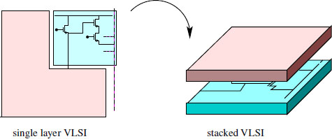
Figure 3.7. Stacked schema. On the left, diagram of a conventional CMOS: a portion of the sensor is reserved for the electronics VLSI and thus does not contribute to the measurement of the optical flow. On the right: stacked sensor. The whole sensor is available for the optical path (on top), the electronic path is delegated to another circuit (at the bottom) which is placed on the rear face of the optical path
3.2.6. Influence of the choice of technology on noise
We have seen that the image of a CCD sensor benefits from a great processing homogeneity. The main cause of image inhomogeneity derives from the effects of geometry which penalize the peripheral sensors [MAR 10]: the pixel vignetting that we have seen in section 2.8.4.1.
However, in the case of CMOS, counting can be affected by a precision up to a pixel; if it is flawed, the pixel is erroneous. This can have two different causes:
- – a non-uniformity of the dark signal (DSNU = dark signal non-uniformity), which depends on the material and on the geometry of the assembly;
- – a non-uniformity of the photo-reponse (PRNU = photo response non-uniformity), which depends on the processing electronics.
We will see in Chapter 7, how these problems manifest themselves and how they are modeled.
3.2.7. Conclusion
The considerable progress accomplished with the CMOS sensor makes it today the best photodetector for photography. They fully benefit from the continuous progress of microelectronics while CCDs can only rely on investments specific to this sector. A very large amount of flexibility have just been allowed by the development of stacked technology. Furthermore, it is very likely that we will see in the forthcoming years an increase in the performance of these sensors, by fully taking advantage of the benefits offered by the new silicon surfaces made available.
3.3. Integrated filters in the sensor
We have just examined photoreceptors and their associated electronics. However, it is not possible to disregard this point of optical elements which are built jointly to the photodetector. In addition to anti-reflective layers which are essential to limit losses at the interface level, two optical accessories can be added to the sensors: chromatic filters and lenses that enable the convergence of the selected channels toward the photosite. In some cases, an item can be added not by integrating it with the photodetector but by attaching it on top: the anti-aliasing filter (see section 3.3.2).

Figure 3.8. Cross-sectional view of a CMOS circuit comprising, in addition to the layers of the photodetector, the chromatic selection elements (Bayer mosaic) and the microlenses. The dimension of such a device is typically in the order of 5 μm between adjacent lenses
3.3.1. Microlenses
As shown in Figure 3.8, the microlenses are practically placed on the photodetector and are as numerous as the photosites (of the order of 10–20 million per sensor) and of the same size (less than 10 μm). Their objective is not to form an image, but to group the rays in order to ensure that the largest number easily reaches the sensor. This significantly loosens the constraints on their optical characteristics.
Most microlens arrays are made of a unique material (usually a high index polymer, but very transparent), whose profile is adapted: it is often a half-sphere built on a base (for manufacturing and rigidity reasons) whose other face is flat. In certain cases, we encounter aspherical profiles. It is also possible that plates with lenses on both faces be found [VOE 12].
These lenses are usually manufactured by molding from a liquid polymer completed by electrolytic machining. Electro-optical processing then takes place to treat and harden the material thus formed (this is the technique known as wafer level optics WLO). The positioning of the optical layers on the photodetector wafers is a very delicate stage, controlled today with an accuracy of 0.25 μm. The cost of the fine positioning of the lenses is higher than that of the lens itself [VOE 12].
During the design of the sandwich (sensor plus microlenses) in high-end systems, pixel vignetting phenomena at the edge of the field can be taken into account (see section 2.8.4). Either the microlens array then presents a step slightly different from that of photosensors, or the lenses offer on the edges of the field an adapted profile, or finally the lenses index varies regularly from the center to the edge. It should be noted that, when the dimension of the photosites becomes very small (in practice less than 1.5 μm), the diffraction effects in the material itself which constitutes the sensor as well as the protection surfaces make the lenses very ineffective. It is imperative to use thinner or back-side illuminated sensors (Figure 3.6) [HUO 10].
Two variants can be seen to emerge and that can substitute for spherical microlenses arrays:
- – micro-Fresnel lenses that replace the half-sphere by portions of spheres, or even by simple rings with constant thickness (zone plates);
- – gradient-index lenses that are embedded in a material with parallel faces but whose index is variable above each photo sensor, according to a radial symmetry distribution law decreasing from the center to the edge.
The role of microlenses is very important, especially when using lenses with short focal lengths (fisheye-type) and very open objective lenses ([BOU 09], page 100).
3.3.2. Anti-aliasing filters
The elements that have an influence on the resolution of a digital image are:
- – the sensor resolution, that is the size of the elementary cell that collects the energy;
- – the focusing, which takes into account as we have seen in section 1.3.4, the relative position of the object point with respect to the plane of focus as well as the aperture of the lens;
- – the aberrations that degrade this focusing (see section 2.8);
- – the diaphragm diffraction (see section 1.3.3).
In some configurations, these filters are insufficient to prevent spectrum-folding phenomena (or aliasing) which show in the image unwanted frequencies on periodic textures. In order to reduce this effect, many devices have an optical anti-aliasing filter which, paradoxically, will physically degrade the impulse response of the camera to improve the image [ZHA 06]. Others carry out a strongly nonlinear a posteriori filtering of the image (we will examine these methods during the demosaicing stage in section 5.5). Moreover, it is the trend in modern cameras.
We will examine how an optical anti-aliasing filter works.
It is mounted on a glass layer placed just in front of the sensor (see Figure 3.9, on the left), generally in front of infrared (warm filter) and ultraviolet (cold filter) filters when they exist and in front the chromatic filters which carry out the matrix conversion of the colors. The filtering function is ensured by a birefringent layer (for example, a lithium niobate crystal). The image is carried by an electromagnetic wave that can be polarized (if such a filter is employed in front of the lens) or not. During the traversal of the glass, a uni-axis medium, the wave is split into two orthogonally polarized rays (see Figure 3.9, on the right): one ordinary, the other extraordinary. This second ray is deflected by an angle ε in accordance with the mechanisms of birefringence [PER 94]. It exits the glass parallel to the incident beam, but laterally shifted to δ = e tan(ε) ≈ eε. It is essential that e be equal to the interpixel distance, such that two neighbouring cells receive the same signal, thus dividing by two the resolution and therefore the bandwidth of the image and thus reducing aliasing in this particular direction. In order to also reduce the aliasing in the second direction, a second glass layer of LiNb03 is placed crossed with the first. Four image points are thus obtained instead of just one. The resolution has been degraded by two in each direction to reduce (without removing it) the aliasing. In non-polarized light, the four images carry the same energy (if using a polarizing filter upstream from the objective, for example, to eliminate reflections on water, the image intensity will depend on the orientations of the axis of the crystal and of the polarizer).

Figure 3.9. Anti-aliasing filter: on the left, positioned in front of the sensor; on the right, beam traversing the lithium niobate crystal, giving rise to two offset beams
How should the axis of the crystal be positioned in order to form a good quality image? Note that the image beam is not a parallel beam when it arrives on the sensor, but it is open with an angle ω fixed by the diaphragm. It is necessary that both ordinary and extraordinary beams remain converging on the sensor. It should be recalled that the extraordinary index nθ seen by a wave forming an angle θ with the crystal axis verifies:
For a beam composed of rays ranging between θ – ω and θ + ω, it is necessary to choose θ in the vicinity of an extremum of equation [1.3] such that the excursion of the index nθ±ω be minimal. This is achieved if the optical axis makes an angle of 45° with the face of the layer and corresponds to an extraordinary index of 2.24 (for lithium niobate, no = 2.29 and ne = 2.20), and a deflection angle of 45 milliradians between the ordinary and the extraordinary beam. A 100 microns thick layer therefore results in an offset δ = 45.10−3.100 = 4.5 μm compatible with the interpixel step.
Figure 3.10, on the one hand, presents the effects of aliasing on periodic structures, on the other hand, the effect of the anti-aliasing filter on the image.

Figure 3.10. On the left: two images presenting spectrum folding defects on periodic structures of corrugated iron: moderate on the left and very accentuated at the center. On the right: effect of the anti-aliasing filter. The image is the macrophotography of an object containing, on the one hand, a Bayer mosaic superimposed on a CMOS sensor, on the other hand, a small scale whose gradations are 10 micrometers apart. The upper part is obtained with a layer of anti-aliasing filter: the image is then doubled at a very close distance of the photodetectors step. At the bottom, the image is taken without anti-aliasing filter and therefore presents a much sharper image, in this image without any risk of aliasing
(©MaxMax: www.maxmax.com/)
In 2014, the first switchable anti-aliasing filters made their appearance. Instead of using a naturally birefringent glass layer, they use a material with induced birefringence by application of an electrical field (electro-optic effect), either by the Kerr effect or Pockels effect. They allow switching quickly from an anti-aliasing filtering position to a position without filtering.
However, a tendency to delegate the processing of spectrum folding to software programs during the demosaicing process, without any involvement of an anti-aliasing filter is also very sensitive. This fact suggests that ultimately the solution with a polarizing filter could be reserved for systems only equipped of very tiny photosites and without enough computing power available.
3.3.3. Chromatic selection filters
These are very important elements of the camera since it is through them that color images are created from mainly panchromatic sensors. We will examine in a very detailed manner later in this book, on the one hand, the geometry of filters (in particular of the Bayer array which constitutes the bulk of sensors on the market) and its influence on image quality (section 5.4), and on the other hand, their colorimetry and the inversion process of subsampling, a process called demosaicing (see section 5.5).
We provide a few elements about the physical production of these filters [MIL 99], a stage that for a long time was one of the most extensive of the manufacture of sensors, causing manufacturers to design them separately from photoreceptors and then to assemble them. Those days are over and chromatic filters are now designed during the same process.
They are laid down by photolithography during the final stages of sensor manufacture and therefore on the sensor surface, and will only be covered by the microlenses. Infrared and ultraviolet filters (hot and cold) will be added at a later stage and mechanically fixed.
They are usually constituted of organic dyes or pigments in a photoresist array. The dyes are distinguished from pigments by a strong chemical interaction between the substrate and the absorbing molecule. Pigments offer a better resistance to temperature and to light exposure necessary for their layering; as a consequence, they have been preferred over dyes in recent years.
The layers are very thin, of the order of the micrometer. Photoresists and dyes are successively layered down and combined to achieve good selections of wavelengths in order to produce positive filters (RGB) or negative (CMY) (see Chapter 5). Complex chemical and thermal processes are brought forward in order to guarantee the success of the processes of, on the one hand, lithography and on the other hand substrate coloration. They often have contradictory effects, which explains the slowness of the generation processes which initially ran for several weeks and are now reduced to a few hours.