
In Chapter 1, we introduced some basic concepts relating to server hardware, concepts such as processor type, multi-processor architecture, and virtual memory to name but a few. There are lots of buzzwords and acronyms that we get bombarded with in this industry. As IT advocates, we need to see past all that and get to the core issues—ask the key questions and get to the heart of the matter. I am sure that some of you are fluent in the ways of computer architecture, while others of you may need a little refresher course on some key elements of architectural design. When it comes to high performance computing, there is much to be gained by knowing and understanding the building blocks our systems are built on, even down to the conceptual design of the CPU cache. As we see, this can have a significant bearing on performance. Then some people ask the question, “Even if the design isn't the best, what can I do about it?” This is a salient point and needs to be addressed. The short answer in most cases is there is nothing we can do about it. It is up to the application developers to understand the data model they used to design the application and how that will be affected by the size and mapping function used to access cache lines. It is not uncommon that subsequent data records, e.g., employee records, happen to be mapped to the same cache line simply by virtue of the size of each record. This can lead to the cache being unloaded and reloaded for each data structure where a simple redesign of the data model could have meant that the data structures loaded to successive cache lines. This could save on average 200-300 CPU clock cycles every time a data structure is referenced.
This appendix is not designed to go into every facet of computer architecture but to give an overview of some key concepts starting with basic processor design and continuing through to aspects of multi-processor architecture such as non-local memory.
I have found that too often people ignore and underestimate the importance of appreciating the workings of the processor. After all, it is the processor that executes instructions to do the work our systems were designed to accomplish. Since the first computer was designed, engineers have strived to push processor performance to achieve more and more. I remember being taught a principle about getting more work done:
Work harder: In terms of a processor, this can mean increasing the clock speed of the processor and/or increasing the density of transistors on the processor itself. Both of these solutions pose problems in terms of heat dissipation, purity of raw materials, and production costs. Processor architects are now finding that the density of transistors on processors can cause electromagnetic effects at the quantum level, known as quantum tunneling. This precludes significant further miniaturization using current materials and fabrication techniques. As always, processor design is a trade-off between what the architects would like to do and what will make a profit for the organization.
Work smarter: Here, we need to look at the overall architecture of the processor. We have just noted that processors may be reaching some fundamental brick walls in terms of quantum level effects in the materials used to construct processors. Over the last few decades, we have seen different processor families emerge, which take different approaches to how the processor operates. We are thinking of CISC, RISC, Vector, and VLIW processors.
Get someone else to help you: I am thinking of two ways in which we can get someone else to help. First, we'd have help on the processor itself. This is a common occurrence in the form of a co-processor. Nowadays this is at least a floating-point co-processor. Many computations involve floating-point numbers, i.e., fractional numbers like 3.5. The other help we are thinking of is having more than one processor. The design of a multi-processor machine has many design criteria. Some of the more common multi-processor architectures include SMP, NUMA, CC-NUMA, NORMA, MPP, and COWs. The decision to choose one architecture over another can be based on cost, flexibility of configuration, the type of computing problems expected, what the competition is doing, as well as conformance with current industry standards.
We can think of the basic functioning of a simple processor by considering what it is designed to do: execute instructions. The closest we can come to seeing an instruction is via a language known as assembly language, sometimes known as assembler. Instructions can take many forms: arithmetic, shift, logical, and floating-point instructions to name a few. Considering this basic functionality, we can further break it down into a basic architecture. Here goes. The processor performs these functions:
Fetches an instruction
Decodes that instruction
Fetches any data that instruction refers to
Executes the instruction
Stores/preserves the result for further processing
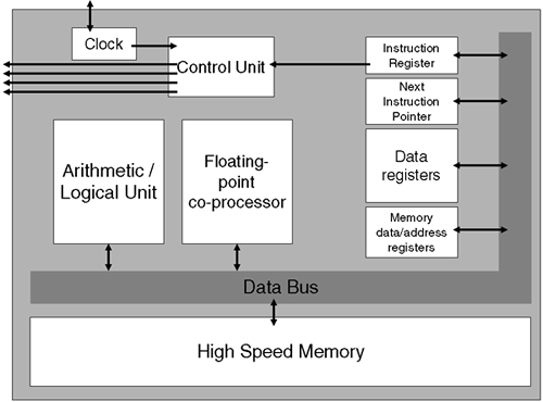
We call this the fetch-execute cycle. Most of the computers we deal with in the business world use this basic philosophy and are known as stored-program computers. Let's take another step in further defining this architecture by drawing a diagram of a simple processor and explaining what the basic components are intended for (Figure A-1):
Note: Not all connection paths and components are necessarily shown. This is a simplified model of a processor. In today's processor architectures, you may have many more esoteric components such as shift/merge, multiply, cache, TLB, and branch management circuitry. This simplified model is used to ensure that we understand the basics.
High-speed memory: Instructions and data (simple data items or the results of previous instructions) are all stored in memory before being acted on by the processor.
Data bus: This connects two or more parts of the processor. The connections between individual components and the data bus are indicated by black arrows over which several bits (usually a data word) can move simultaneously.
Arithmetic/logical unit (ALU): This is the brain that performs arithmetic and/or logical operations, e.g., ADD, NEGATE, AND, OR, XOR, and so on.
Floating-point coprocessor: This performs similar operations as the ALU but does so on floating-point numbers. On decoding an instruction, the control unit decides whether we are using integers or floating-point numbers.
Memory data/address registers: Processors may use special purpose registers to temporarily hold the address and/or the data of the next expected datum. Some architectures use this philosophy heavily for prefetch and branch prediction technologies.
Next instruction pointer (NIP or program counter): This is another special purpose register. Again, architectures may or may not use this idea heavily. The idea is that with NIP we know where in high-speed memory the next instruction is physically located.
Instruction register: This is the special purpose register holding the instruction currently being executed.
Control unit: This directs and controls the various components of the processor in performing its tasks, e.g., a general-purpose data register to open its output path in preparation for a data item to be transferred to the ALU. The unidirectional arrows that appear to go nowhere lead to other parts of the processor, memory, and other components such as the IO subsystem. They carry control signals to coordinate activities between the processor and other components, e.g., control signals known as interrupts coming from external devices such as the IO subsystem.
Clock: This determines the speed of operations. It normally operates at clock frequencies measured in megahertz, and the frequency is sometime referred to as the clock period. The ideal for a processor is to execute every instruction every clock period; an easy way to remember this is “every tick of the clock.” However, this is seldom the case, except with possibly the most primitive of operations, i.e., arithmetic and logic operations on integers. The time to execute an individual instruction is commonly measured in multiples of the clock period, e.g., it is not uncommon for a floating-point instruction to take three ticks to complete. The latency (the amount of time it takes) to perform different types of operations goes some way toward determining the overall performance of a system and helping to demonstrate the efficiencies of the underlying architecture. The clock usually has some form of external repeating pulse generator, such as a quartz crystal.
Data registers: I have left these for last to include a brief description of the registers themselves. Registers are known as bistable devices, and sometimes known as a “flip-flop” because it is an electronic device made up of elements such as transistors and capacitors, capable of exhibiting one of two states (on=1 off=0) in a consistent fashion. A register of n bistables can store a word of length n bits: hence, a 64-bit register can store a 64-bit value. This doesn't mean that it's necessarily a 64-bit integer. Some instructions may be expecting a 32-bit integer and, hence, we could achieve a form of parallelism by performing a single data load, but in doing so we have access to two data elements. This is sometimes referred to as an SIMD (Single Instruction Multiple Data, from Michael Flynn's 1972 Flynn's Classification) architecture. In an ideal world, all our data and instructions would be stored in registers. Because the physical space on the processor is limited, we are usually limited to tens of registers—some special purpose, some general purpose. A simple way to distinguish between the two types of registers is that general-purpose registers can be named explicitly in instructions, while special purpose registers cannot be named explicitly by instructions, but are controlled explicitly by the control unit.
So let's revisit out basic architecture and flesh out the fetch-execute cycle.
The next instruction to be executed is fetched from memory into the special-purpose register designed to hold it. At this point, the NIP is updated to point to the next instruction to be executed.
The control unit decodes the instruction and if necessary instructs other components on the processor to perform certain tasks. Implicit in this step is the fact that in decoding the instruction we now know whether we need any operands (the datum to be operated on) and how many, e.g., an architect designer will normally require two operands for an ADD operation as well as a target register to store the result.
The control unit causes the operands to be fetched from memory and stored in the appropriate registers, if they are not already there.
The ALU is sent a signal from the control unit to carry out the operation.
The result is temporarily stored in the ALU before being written out to the target register.
The next instruction is fetched and executed.
And the cycle continues.
Even at system boot-up time, we can see how this fetch-execute cycle would operate at a primitive level:
A special-purpose processor performs Power On Self Test (POST) operations.
The NIP is loaded with the first instruction to be executed to get the operating system up and running, i.e., the starting address of the operating kernel.
Obviously, this is a simplified description, but once we understand this basic operation, we can then move on to discuss more complicated models and appreciate the technological choices and challenges faced by processor designers.
We have spoken of a simple processor exhibiting a simple architecture. The design of our Instruction Set Architecture needs to accommodate all the design goals we laid out in our initial processor design. In reality, we need to think about more complex architecture considerations in order to maximize our processor performance. For example, while the control unit is decoding an instruction, the electronics that make up the ALU are sitting idol. Wouldn't it be helpful if each individual component could be busy all the time, coordinated in a kind of harmonic symphony of calculatory endeavors.
A further motivation for conducting this orchestra of components dates back to the 1940s and 1950s. Two machines developed during and after the Second World War laid down the design of most current machines. The underlying architecture born from these ideas is known as the von Neumann architecture. John von Neumann designed EDVAC (Electronic Discrete Variable Automatic Computer). This was one of the first[1] computers to store instructions and data as essentially a single data stream. This model makes for a simplified and succinct design and has been the cornerstone of most computer architectures since then (other architectures do exists, for example, the reduction and dataflow machines; however, they are not used widely in the business arena). The von Neumann architecture can have an impact on overall processor performance because with both data and instruction elements being viewed as similar datum, they have to follow essentially the same data path to get to the processor. Being on the same data path means that we are dealing with either an instruction datum or data datum, but not both simultaneously. The problem of only doing one thing at a time has become known as the von Neumann bottleneck. If we can do only one thing at a time, this has a massive impact on the overall throughput of a processor. One well-trodden path to alleviate the effects of the von Neumann bottleneck is simply to increase the speed of the processor. With more instructions being executed per clock period, we hope to get more work done overall. As mentioned previously, there is only so far we can take that work harder ethic with current materials and fabrication methods. To try to work around the von Neumann bottleneck, we need to also work smarter. This is where processor designers have some interesting design decisions to make.
While we could simply work harder and continue to increase the clock speed of our processors, eventually effects such as quantum tunneling will mitigate any further development in that particular field of study. Not to be outdone, there are some cunning ways in which processor architects can extract more and more performance without resorting to mega-megahertz. Let's look at some of the tricks that processor architects have up their sleeves to alleviate the problems imposed by the von Neumann bottleneck.
A scalar processor has the ability to start only one instruction per cycle. It follows that superscalar processors have the ability to start more than one instruction per cycle. This allows the different components of the processor to be functioning simultaneously, e.g., the ALU and the control unit can be doing their own things while not interfering with each other. In order to utilize this idea, we need an advanced compiler that can generate a generous mix of instruction types, e.g., floating point, integer, memory, multiply (if you have an independent Multiply Unit), so that a processor can be seen to be scheduling more than one instruction every clock period. Even though it appears to be scheduling more than one instruction per clock period, each component is still limited by the von Neumann bottleneck; each component is doing only one thing. The difference is that collectively the entire processor is getting more work done in a given time period. This introduces a level of parallelism into the instruction stream. Parallelism is a fundamental benefit to any processor. Some advanced processors also have built-in circuitry such as branch prediction and/or instruction reorder buffers to help implement a superscalar architecture. The idea behind this additional circuitry is to allow the processor to operate in a wider set of circumstances where an advanced compiler may not be available. Having both an advanced processor and advanced intelligent compilers can produce phenomenal results. When migrating a program from one particular architecture to another, you will probably have to recompile your program. If the new architecture offers backward compatibility, you need to ask yourself, “Do I still want to do it the old way?” It is always sound advice to recompile a program from an older scalar architecture when you move it to a superscalar architecture, or even between versions of an existing superscalar architecture. This ensures that the new intelligent compiler generates an optimum mix of instructions to take advantage of the new processor's features. Processors that can schedule n instructions every clock period are said to be n-way superscalar, e.g., 4 instructions per cycle = 4-way superscalar. Several HP processors have used a superscalar architecture in the recent past. Table A-1 shows some of them.
Table A-1. HP Scalar and Superscalar Processors
PA-RISC version | Models | Characteristics |
|---|---|---|
*HP-UX Tuning and Performance, Prentice Hall, 2000. | ||
PA 1.0 | PN5, PN10, PCX | Scalar implementation One integer or floating-point instruction per cycle 32-bit instruction path |
PA 1.1a | PA70000, PCX/S | Scalar implementation One integer or floating-point instruction per cycle 32-bit instruction path |
PA 1.1b | PA71000, PA7150, PCX/T | Limited superscalar implementation One integer and one floating-point instruction per cycle 64-bit instruction path (2 instructions per fetch) |
PA 1.1c | PA7100L, PCX/L | Superscalar implementation Two integer or one integer and one floating-point instruction per cycle 64-bit instruction path |
PA 1.2 | PA7200, PCX/T | Limited superscalar implementation One integer or floating-point instruction per cycle 64-bit instruction path (two instructions per fetch) |
PA 2.0 | PA8000, PA8200, PA8500, PA8600, PA8700, PA8700+ | Two integer and two floating-point and two loads or two stores per cycle 64-bit extensions 128-bit data and instruction path |
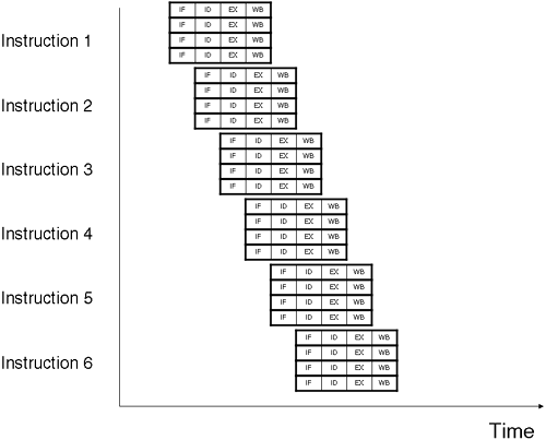
An easy analogy to visualize processor pipelining is to visualize a manufacturing production line. To make a widget, you need to break down the construction process to discreet production stages. Ideally, each production stage is of a similar length so that workers in subsequent stages are not left hanging around waiting for a previous stage to finish. If everyone is kept busy with his or her particular part of the process, the overall number of widgets produced will increase. In a similar way, we can view the pipeline of instructions within a processor. If a large, complex procedure can be broken down into easily definable stages and executing each stage takes the same amount of time, we can interleave each stage in such a way that individual parts of the processor circuitry are performing their own stage of the instruction. Let's break an instruction down into four stages.
Instruction Fetch (IF): Instruction fetch.
Instruction Decode (ID): Instruction decode; may include fetch data elements referenced in the instruction.
Execute (EX): Execute the Instruction.
Write Back (WB): Write back the result.
If we assume that each stage takes one unit of time to execute, then this instruction would take 4 units of time to complete. Breaking down the instruction into distinct stages means that we can interleave the commencement of the next instruction before the previous instruction completes. Figure A-2 shows the effect of pipelining.
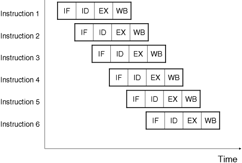
In a non-pipelined architecture, executing the instruction stream shown in Figure A-2 would have taken 6 x 4 =24 units of time. With pipelining in place, we have reduced the overall time needed to execute the instruction stream to an amazing 9 units of time. It is apparent from Figure A-2 that adding an additional instruction adds only 1 additional unit of time into the overall execution time. With a small instruction stream like the one in Figure A-2, we have achieved an amazing 267 percent speedup! With a large number of instructions, we actually approach the situation where
This ideal maximum where the speedup equates to the number of stages in the pipeline is again a nirvana we seldom see. It does rely on the factors that we mentioned previously:
Every instruction is broken down to exactly the same number of stages.
All stages take exactly 1 unit of time to execute.
All stages can operate in parallel.
The instruction stream is always full of useful instructions.
This ideal scenario seldom exists with a real-world instruction stream. For this to be the case, every program ever executed would have to be entirely linear, i.e., no branches, loops, or breaks in execution. Another factor that can go against the maximum possible speedup is the fact that pipelining an instruction into discreet stages requires additional logic within the processor itself. This takes the form of additional circuitry in the form logic gates which, in turn, are made up of individual electronic components. With the real estate on a processor being so expensive (remember the density of transistors, data paths, and so on, on a processor increases the cost of manufacture and increases the probability of errors, which push the price of processors ever higher), the number of discreet stages in the pipeline is another design decision that the processor architect needs to make.
As mentioned above, an aspect of pipelines that can mitigate achieving maximum speedup is the nature of a real-life instruction stream. Programs commonly loop and branch based on well-known programming constructs, e.g., if-then-else, while-do, and so on. This poses problems for the compiler as well as the processor. Loops and branches interrupt the sequential flow of a program and require a jump to some other memory location. Knowing when this is going to happen and, more difficult, where we are going to jump to is not the easiest thing for the architecture to predict. However, many optimizing compilers as well as specially designed circuitry on the processors themselves go a long way toward circumventing a problem known as pipeline hazards. We see essentially three types of pipeline hazards:
Control hazards: Some hazards are due to instructions and/or branches changing the sequential flow of the program. When we have such a situation, e.g., an
if-then-elseconstruct, we may find that we need to branch to a previous location to restart the pipeline. This would require flushing the pipeline and starting again. During this flushing, the processor is not executing useful instructions. One technique used to get around this is called a delayed branch where the compiler predicts a branch (it can see it coming in the instruction stream and it knows a branch is going to slow things down) and performs it earlier than expected because it knows on average how long the branch will take. In the time it takes the process to jump to the new memory location, the processor can be executing non-related but otherwise useful instructions. The ability of the processor to reorganize the instruction stream on the fly is sometimes referred to as out of order execution. This capability can be hardwired into processors themselves, at a cost. Should the reorganization introduce other hazards, the processor needs to be able to flush the completion queue in order to back out the previously executed instructions. Such additional circuitry is reducing the available real estate on the processor itself. The idea of predictive intelligence can also be built into optimizing compilers. We can also assist the processor in predicting what happens next by running applications many times with typical input streams. In this way, we are building a profile of a typical instruction stream that the compiler can use to further optimize the application, which is also known as profile-based optimization.Data hazards: It is not uncommon for one instruction to require the result from a previous instruction, as in these two equations:
x + y = z)
z + a = b
The second equation is dependent on the result from the first. The processor would need to ensure that the value of z is written back (the WB, or Write Back, stage has not completed) to memory before calculating the second equation. A number of methods can be used to alleviate these problems. Similar to the way in which branch delay slots work, a designer may use load delay slots to alleviate data hazards. As an example, take the instruction
LOAD r2, locationA, where we are loading registerr2from memory locationlocationA. ALOADinstruction will take an amount of time for the memory bus to locate the datum in memory and transfer the value to the register; possibly several clock periods. While this happens, the registerr2may have a previous value still stored in it. If the next instruction to be executed also referencedr2, for exampleSUB r2,r1,r2, the instruction stream has inadvertently introduced a data hazard; while theLOADis completing, we have an instruction which is in effect using the old value ofr2. This particular hazard is known as a read-after-write (RAW) hazard and can cause the pipeline to stall while the instruction stream is rolled back to a point where theLOADinstruction was executed. We sometimes see write-after-write (WAW) and write-after-read (WAR) hazards that are caused by similar issues in the instruction stream. One solution to get around this type of problem would be to use a load delay slot. As the name suggests, whenever aLOADis executed, a delay is inserted (usually aNOOPinstruction) into the instruction stream. This is designed to allow theLOADto complete before the next instruction starts executing. This is not very practical. The architect would have to insert enough load delay slots to accommodate the worse-case scenario when aLOADtakes an inordinate amount of time to complete. An alternative solution would be to stall the processor: Immediately following aLOAD, the processor is effectively frozen until theLOADcompletes. This has been seen to be a better solution than inserting lots ofNOOPs.Structural hazards: Structural hazards can be caused by limitations in the underlying architecture itself, i.e., the architecture is not able to support all permutations of instructions. Remember that we are probably dealing with a von Neumann machine where data and instructions are treated the same. To
LOADa data element and an instruction simultaneously goes against the von Neumann bottleneck because both are treated as equals. Both data and instructions are stored in main memory as a stream of data points; they are both effectively seen as data. As a result, both data and instructions share the same data path to arrive at the processor. Designers can alleviate this by utilizing two separate memory buses for data and instruction elements. In these situations, designers may also employ separate data and instruction caches (more on cache memory later).
A word of warning: Some people think that pipelining and superscalar are essentially the same—if not identical, then quite similar. They may appear similar, but they are definitely not the same. Superscalar, simply put, is the ability to start more than one instruction simultaneously. Many architectures employ superscalar processors. Not all architectures can easily employ pipelining. As we have seen, to employ pipelining to its maximum benefit requires all instructions to be decomposed to the same number of stages, all stages take the same amount of time to execute, and all stages can operate in parallel. This is not necessarily achievable in every situation. What we are aiming to achieve with pipelining is an improvement in the overall cycle time for the execution stream. With superscalar architectures, we are hoping to achieve the same improvements with instruction throughput. We may have a four-way superscalar processor, but if each instruction is a not easily decomposed into discreet individual stages, then each instruction is still taking a significant length of time to complete. Statistically, we should achieve more throughput simply because more instructions are being executed simultaneously as a result of the superscalar architecture. If we can achieve both superscalar and pipelining, we can see even more significant improvements in the performance. Some newer architectures are even claiming to be super-pipelining whereby individual instructions are being decomposed even further to try to ensure that as many individual circuits in the processor are working simultaneously.
The size of objects on a processor is an important feature in design. Accommodating 64-bit instructions requires significantly more processor hardware than a 32-bit instruction simply because we need more bits to store a 64-bit instruction than a 32-bit instruction. Remember, instructions will be represented by binary digits: 1s and 0s. Having a larger instruction does give you more flexibility as far as instruction format, the number of different instructions in your instruction set, as well as how many operands an instruction can operate on. Before we go any further, let's remind ourselves again about some numbers:
32-bit = 232
A 32-bit instruction gives us 4,294,967,296 permutations of instruction format and number of instructions. For most architectures, an instruction size of 32 bits yields more than enough instructions. However, limiting an architecture to 32 bits also limits the size of data elements to 32 bit. This means that the largest address we can use is 232 = 4GB. An address space of 232, i.e., 4GB, limits the size of individual operating system processes/threads. This is a major problem facing applications today. Many applications require access to a larger address space. This requires the underlying hardware to support larger objects. Today's processors support 64-bit objects.
64-bit = 264
A 64-bit instruction set gives us quite a few more permutations. In fact, the number of permutations goes up to 18,446,744,073,709,551,616 which equates to 16 Exabytes (EB). Most 64-bit operating systems do not require the full 16EB of addressing space available to them. We now have machines that have more physical memory than can be accommodated by a 232 (4GB) operating system. In order to utilize more than 4GB of RAM, the operating system must be able to support larger objects. In turn, for the operating system to support larger objects, the underlying architecture must support these larger objects as well. Although many architectures support 64-bit objects, it is not uncommon for instructions to be 32 bits in size. Remember, a 32-bit instruction still gives the instruction set designers 232 different instructions. We can achieve an additional parallelism with 32-bit instructions in a 64-bit architecture; we can fetch 2 instructions per
LOAD.8-bit = 28. Commonly known as a byte.
Almost every machine now uses an 8-bit byte. One reason for using 8 bits could rest with the notation of what we are trying to represent inside the computer: characters. Take the letter A. It is now convention that this is represented by the decimal number = 65. So our letter A in binary looks like this:
27
26
25
24
23
22
21
20
128
64
32
16
8
4
2
1
0
1
0
0
0
0
0
1
This comes from the ASCII (American Standard Code for Information Interchange) character-encoding scheme developed in 1963. ASCII is actually a 7-bit code. If we were to use all 8 bits, we could represent 0 to 255 = 256 natural numbers and then the ASCII character encoding could represent 256 letters and symbols. But we have learned that we don't need the diversity of symbols: 128, i.e., 7-bits, are enough for the Western character set.
The additional eighth bit could be used to represent negative numbers: known as the sign-bit, with 1 representing a negative value. In reality, computers don't use this sign-and-magnitude representation of negative numbers. A simple explanation as to why the eighth bit is not used as the sign-bit is to take this example:
If we were to use our sign-and-magnitude representation above, our calculations would come unstuck. One thing to remember with binary arithmetic is that 1 + 1 = 0 carry 1. Let's perform our simple calculation using sign-and-magnitude binary representation:
Represent –71 in sign-and-magnitude binary with the most significant bit (leftmost in this case) representing the sign:
Sign-bit
26
25
24
23
22
21
20
Sign-bit
64
32
16
8
4
2
1
1
1
0
0
0
1
1
1
Do the same for –6:
Sign-bit
26
25
24
23
22
21
20
Sign-bit
64
32
16
8
4
2
1
1
0
0
0
0
1
1
0
Now add them together:
Sign-bit
26
25
24
23
22
21
20
Sign-bit
64
32
16
8
4
2
1
1
1
0
0
0
1
1
1
1
0
0
0
0
1
1
0
0
1
0
0
1
1
0
1
The answer comes out as +77. Although this may seem strange to our logical minds, the rules of addition dictate that in binary 1 + 1 = 0 carry 1. The carry 1 is carried to the next position. Somehow, we would need to inform the processor not to process the sign bit; this is what we do mentally, but it would not be straightforward to program a processor to do the same. In this case, we would need a carry bit just in case we meet the situation we see above. The alternative is to use a number representation known as two's complement. This is how computers store signed integers. The name two's complement doesn't give any hint as to how this works, so I'll try my best to explain.
As we saw in the binary numbers above, each bit in a binary number has what we call a weighting: Bit 0 has a weighting of 20 (0), while bit 7 has a weighting of 27 (128). We can use this to convert a decimal number into binary. First, we take the largest power of 2 that is less than the original value. We set this bit to be 1. We subtract the decimal value of that power of 2 from our original value. The remainder becomes our new value. We then subtract successive lower powers of 2 in a similar fashion until we reach 0. Look at decimal 77 as an example:
Weighting | Value | Result | Bit | Remainder |
|---|---|---|---|---|
28 | 256 | 0 | ||
27 | 128 | 0 | ||
26 | 77 | 64 | 1 | 13 |
25 | 32 | 0 | ||
24 | 16 | 0 | ||
23 | 13 | 8 | 1 | 5 |
22 | 5 | 4 | 1 | 1 |
21 | 2 | 0 | ||
20 | 1 | 1 | 1 | 0 |
Reading from the top: 7710 = 10011012 | ||||
This is one way we convert decimal numbers into binary. In two's complement, bit 7 has a weighting of –27 (-128). We then construct our numbers using these new weightings. Let's take our original example of –71 and represent it using two's complement:
-27 | 26 | 25 | 24 | 23 | 22 | 21 | 20 |
-128 | 64 | 32 | 16 | 8 | 4 | 2 | 1 |
1 | 0 | 1 | 1 | 1 | 0 | 0 | 1 |
When we consider the weightings, -27 + 25 + 24 + 23 + 20 = -128 + 32 + 16 + 8 + 1 = -71, –6 becomes:
-27 | 26 | 25 | 24 | 23 | 22 | 21 | 20 |
-128 | 64 | 32 | 16 | 8 | 4 | 2 | 1 |
1 | 1 | 1 | 1 | 1 | 0 | 1 | 0 |
-27 + 26 + 25 + 24 + 23 + 21 = -128 + 64 + 32 + 16 + 8 + 2 = -6
We can now perform our original calculation using the two's-compliment representation:
-27 | 26 | 25 | 24 | 23 | 22 | 21 | 20 |
-128 | 64 | 32 | 16 | 8 | 4 | 2 | 1 |
1 | 0 | 1 | 1 | 1 | 0 | 0 | 1 |
1 | 1 | 1 | 1 | 1 | 0 | 1 | 0 |
1 | 0 | 1 | 1 | 0 | 0 | 1 | 1 |
When we look at the weightings, we see -27 + 25 + 24 + 21 + 20 = -128 + 32 + 16 + 2 + 1 = -77.
The clever part with two's complement arithmetic is that even if you have a carry-bit, it can always be ignored.
A word:
A word is an indeterminate value. It can take many forms, but its size is usually the normal processing unit used by the processor, e.g., a 64-bit processor will work with a 64-bit word. A word is usually big enough to store either a single instruction or integer. It most often takes the form of an integer multiple of bytes.
Some other numbers to consider:
1 kilobyte (KB) = 1024 bytes
1 megabyte (MB) = 1024 KB
1 gigabyte (GB) = 1024 MB
1 terabyte (TB) = 1024 GB
1 petabyte (PB) = 1024 TB
1 exabyte (EB) = 1024 PB
1 zetabyte (ZB) = 1024 EB
1 yottabyte (YB) = 1024 ZB
Our original question about size was related to the size of an instruction itself. Do we really need 264 possible permutations for the format of a single instruction? Probably not. There is more than enough flexibility in a 32-bit instruction. Consequently, a designer could elect to have variable size instructions. The benefit would be that for simple, smaller instructions the processor only has to fetch a few bits, speeding up the fetch cycle. However, somewhere in the logic of the processor, it would need to know how big the next instruction was. This would be some other architectural feature that would need to be built into the processor hardware and logic circuitry: Again, that's a design tradeoff. Registers that can accommodate 64-bit values can be seen as a bonus because data elements stored in the register can represent big numbers. A register that can accommodate a 64-bit value means that the value stored in a register could actually be the address of a memory location. This in turn means that we can have 264 worth of physical memory in our machine. Having a data path (a microscopic wire or connector inside the processor) that can transfer 64 or even 128 bits simultaneously is a desirable feature because you can move lots of data round quicker. As we can see, design tradeoffs have to be made in many aspects of the processor design.
Before an instruction can actually do something, it needs to locate any data elements (called operands) on which it is supposed to be working. The instruction will use an address to locate its operands. The complicating factor is that an address may not be a real memory location, but rather a relative address, relative to the current memory location. This interpretation of an address is coded into the instruction and is known as the addressing mode. Architects can choose to use different addressing modes. The type and number of addressing modes used will have an impact on the actual design of the instructions themselves. Here are some of the more common addressing modes used:
Immediate addressing: This is where the memory location follows immediately after the instruction, e.g.,
ADDIMMEDIATE 5. The data element5is located immediately after the instruction. This means “add 5 to whatever is currently stored in the ALU/register.”Direct addressing: This is where the operand following the instruction is not the actual data itself but the memory location of where to find the real data, e.g.,
ADDDIRECT 0x00ef2311means “add the contents of the ALU/register to the data you find at address0x00ef2311.”Indirect addressing: This is similar to direct addressing except that the address we pass to the instruction is not the real address of the data, but simply a reference to it; in other words, it behaves like a forwarding point, e.g.,
LOADINDIRECT 0x000ca330means “go to address0x000ca330and there you will find the real address of the data toLOAD.” This can be useful in programming when we don't currently know where in memory a datum will actually be located, but we can use a reference to it in this indirect fashion. A concept known as pointers utilizes indirect addressing.Indexed addressing: When we are dealing with collections of data elements, possibly in an array, it can be useful if we can quickly reference as specific element in that array. Our instruction will be passed the starting address of the collection of data elements and use the content of what we will call and index register to reference the actual data element in question. The index register may be a special purpose register or simply a general register. The instruction will have been programmed by the architect to know how the indexing works.
Inherent addressing: This occurs where an instruction does not use an addresses or the address is apparent, e.g.,
STOPorCLEAR.
We have looked at a number of tricks that the processor architect has to choose when designing his processor. Next, we look at three of the most prevalent families of processors in the marketplace today.
Now that we understand some of the basic functionality of a processor as well as some of the techniques available to designers to try to improve the overall throughput of a processor, let's look at some of the common processor families available in today's computers and which tricks they employ to maximize performance.
Before we explore some of the features of a CISC architecture, let's discuss something called the semantic gap. The semantic gap is the difference between what we want to do with a machine and what the machine will actually do. As we discussed earlier, instructions do things like ADD, SUB, and LOAD. We then ask ourselves, “How does that equate to displaying a graphic on our screen?” The semantic gap between what we want to do, i.e., display a graphic, and what the computer can actually do is rather wide. When programming a computer, it would be convenient if the assembly language instructions closely matched the functions we wanted to perform. This is the nature of high-level programming languages. The programming language closes the semantic gap by allowing us to program using more human-readable code that is subsequently translated into machine code by a compiler. Back in the early days of computing, i.e., the 1950s, compilers were either not very good or simply weren't available. It was common for programmers to hand-code in assembler in order to circumvent the failings of the compiler. Programming in assembler became commonplace. Back then, computers didn't have much memory, so the programs written for them had to be efficient in the use of memory. Being human, we prefer tools that are easy to use but at the same time powerful. When using assembler, if you have a single instruction that performs a rather complicated task, the motivation to use it is high: You can get the job done quicker because your programs are smaller, easier to write, and easier to maintain, e.g., a DRAWCIRCLE instruction is easy to understand and maintain. As programmers, we are not concerned with the resulting additional work undertaken by the processor to decode the DRAWCIRCLE instruction into a series of LOAD, ADD, and SUB instructions. With having fewer individual instructions, there are fewer fetches from memory to perform. If you are spending less time fetching, you can be spending more time executing. Back in the 1950s, accessing memory was very slow, so the motivation was high to perform fewer fetches. The concept of pipelining had not even been considered. Back in the 1950s, computers were all but a few sequential in operation. (IBM developed the IBM 7030—known as Stretch—which incorporated pipelined instructions and instruction look-ahead as well as 64-bit word. The U.S. government bought a number of these machines for projects such as atomic energy research at huge losses to IBM.) The other benefit in those days was that smaller programs took up less memory, leaving more space for user data. Having a myriad of instructions was a major benefit because we could use the instructions we needed to perform the specific tasks required, while at the same time the diversity of instructions made the computer itself attractive to many types of problems. Having a general-purpose computer was a new concept in those days and was a dream-come-true for the marketing departments of the few computer companies that had spearheaded the technology. A crucial element in the design was the size and complexity of the instruction set. In those days, the ideas of superscalar and super-pipelining were the things of dreams and fantasies. If the designers in those days had the materials and technologies available to today's architects, maybe some of their designs would have been different.
The design philosophy behind CISC is to close the semantic gap by supplying a large and varied instruction set that is easy to use by the programmers themselves—supply a large and diverse instruction set and let the programmers decide which instructions to choose. We have to remember the historical context we are working in during this discussion. A processor is a relatively small device packed with transistors that have a finite density. Even in the 1970s and 1980s, the density of transistors was a fraction of what it is now. The fact that we are providing a myriad of instructions does not mean that all the instructions will be executed directly on the processor. In fact, few if any instructions will actually be executed directly on the processor. Standing in their way is a kind of instruction deconstructer. This black box will accept an instruction and decompose it into micro-instructions. These micro-instructions are the actual control logic to manipulate and instruct the various components of the processor to operate in the necessary sequence. This is commonly called micro-programming with the micro-instructions being known as microcode. In this way, we are hiding the complexities of processor architecture from the programmers, making their job easier by supplying the easy-to-use instruction set to construct their programs. The instruction deconstructer or decoder becomes a processor within a processor. An immediate advantage here is that maintaining the instruction set becomes much easier. To add new instructions, all we need to do is update the microcode; there's no need to add any new hardware. An added advantage of this architecture philosophy is that you if we migrate the microcode sequencer to a any new, bigger, faster processor, our programmers don't need to learn anything new; all of the existing instructions will work without modification. In effect, it is the microcode that is actually being executed; our assembler instructions are simply emulated. Looking back to our bag of tricks in Section A.1.3, let's look at which tricks a CISC architect could employ.
Superscalar: Nothing prevents the control logic for the various components on a CISC processor from being activated simultaneously, so we could say that a CISC processor was superscalar.
Pipelining: This is a bit trickier. As we saw with pipelining, the trick is we know that each stage of an instruction will complete within one clock cycle. First, CISC instructions may be of different sizes, so breaking them down to individual stages may be more difficult. Second, due to the complex nature, some stages of execution may take longer than others. Consequently, pipelining is more of a challenge for CISC processors.
Instruction size: Due to the flexibility inherent in the design of a CISC instruction set, instruction size is variable, depending on the requirements of the instruction itself.
Addressing modes: CISC architectures employ various addressing modes. Because any given instruction can address memory, it is up to an individual instruction on how to accomplish this. This also means that we can reduce the overall number of registers on the processor because anyone can reference memory and only when they need to.
It would appear that a CISC architecture has lots of plus points. Once you have sorted out the microcoding, you become the programmer's best friend: You can give them hundreds of what appear to a programmer to be useful instructions. Each instruction is ostensibly free format, with an addressing mode to suit the needs of the programmer. Table A-2 demonstrates that CISC is by no means a dead architecture. Companies like Intel and AMD are investing huge sums of money in developing their processors and making handsome profits from it. The plus points achieved by CISC architectures come at a price. Traditionally, designers have had to run CISC processors at higher clock speeds than their RISC counterparts in order to achieve similar throughput. When some people look at a clock speed of 2.4 GHz, they say, “Wow, that's fast.” I hope that we are now in a position to comment on the necessity for a clock speed of 2.4GHz in a CISC architecture. Is it a good thing or simply a necessity due to the complexity of the underlying architecture?
Table A-2. CISC Architectures
Instruction Set Architecture (ISA) | Processor |
|---|---|
Intel 80x86 | Intel Pentium AMD Athlon |
DEC VAX | VAX-11/780 (yep, the original 1 MIP machine) |
Characteristics of a CISC Architecture | |
Large number of instructions | Complex instructions are decomposed by microprograms called micro-code before being executed on the processor |
Complex instructions taking multiple cycles to complete | Fewer numbers of register sets |
Any instruction can make reference to addresses in memory | Traditionally requires higher clock speeds to achieve acceptable overall throughput. |
Variable format instructions | Multiple addressing modes |
Few processors are entirely based on one architecture. Next, we look at RISC (Reduced Instruction Set Computing) in Table A-3. Some would say it's the natural and obvious competitor to CISC.
Table A-3. RISC Architectures
Instruction Set Architecture (ISA) | Processor |
|---|---|
HP PA-RISC | PA8700+ |
Sun SPARC | Sun UltraSparc III |
IBM PowerPC | IBM PPC970 |
SGI MIPS | SGI MIPS R16000 |
Characteristics of a RISC Architecture | |
Fewer instructions | Simple instructions “hard wired” into the processor, negating the need for microcode. |
Simple instructions executing in one clock cycle | Larger numbers of registers |
Only | Traditionally can be run at slower clock speeds to achieve acceptable throughput. |
Fixed length instructions | |
Fewer addressing modes | |
The RISC architecture has come to the fore since the mid-1980s. Most people seem to think that RISC was invented at that time. In fact, Seymour Cray created the CDC 6600 back in 1964. Ever-diminishing costs of components and cost of manufacture have driven the recent advances in the use of RISC architectures. As the cost of memory fell, the necessity to have small, compact programs diminished. Programmers could now afford to use more and more instructions, because they no longer had to fit a program into a memory footprint whose size could be counted in the tens of kilobytes. We could now have programs with more instructions. At the same time, compiler technology was advanced at a rapid pace. Numerous studies were undertaken in an attempt to uncover what compilers were actually doing, in other words, which instructions the compilers were actually selecting to perform the majority of tasks. These studies revealed that instead of using the myriad of instructions available to it, compilers preferred to utilize a smaller subset of available instructions. The obvious question to processor designers was, “Why have such a large, complex instruction set?” The result was the Reduced Instruction Set Computing architecture (RISC). It is common for a RISC instruction set to have fewer instructions than a comparable CISC architecture. It was not a precursor for a RISC architecture; it's just that RISC designers found that they could utilize their current instructions in clever sequences in order to perform more complex tasks. Hence, the instruction set can stay relatively small. With this in mind, it could be said that it is the complexity of the instructions that was Reducing; as a side effect and natural consequence, the number of those instructions gets reduced at the same time. What we are looking to achieve can be summarized as follows:
Build an instruction set with only the absolute minimum number of instructions necessary.
Endeavor to simplify each instruction to such as extent that the processor can execute any instruction within one clock cycle.
Each instruction should adhere to some agreed format, i.e., they are all the same size and use a minimal number of addressing modes.
This all sounds like good design criteria when viewed purely from the perspective of pure performance. Let's not forget the programmer who has now to deal with this new instruction set. He may not have at his disposal the easy-to-use, human understandable instructions he had with the CISC architecture. What does he do now? The semantic gap between man and machine has suddenly widened. The secret here is to look back to the compiler studies undertaken with CISC architectures. Compilers like simple instructions. Compilers can reorder simple instructions because they are easier to understand and it is easier to predicate their behavior. This is the essence of closing the semantic gap. The gap is closed by the compiler. Some would say that processor architects are simply passing the semantic buck onto compiler writers. However, it is much more cost-effective to write a compiler, test it, tune it, and then rewrite better than to redesign an entire processor architecture. In essence, with RISC we are focusing more on working smarter. With simplified instructions, we are trying to minimize the number of CPU cycles per instruction. CISC on the other hand was trying to minimize the overall number of instructions needed to write a program—and as a result reduce the size of the program in memory. We can immediately identify a fundamental difference in the philosophies of both architectures.
total_ execution_ time= number_ of_ instructions* cycles_ per_ instruction* cycle_ time
CISC: Focuses on reducing the total
number_of_instructionsto write an individual program.RISC: Focuses on reducing the
cycles_per_instructionby utilizing simplified instruction.
If we measure the cycle_time in fractions of a second, cycle_time being directly proportional to the processor speed in megahertz, we can understand why CISC architectures commonly utilize higher clock speeds, while RISC architectures can utilize slower clock speeds but still maintain overall throughput.
Another aspect of RISC architectures that helps to reduce complexity is the addressing modes used by instructions. First, there are usually only two types of instructions that are allowed to access memory: LOAD and STORE. All other instructions assume that any necessary data has already been transferred into an appropriate register. Immediately, this simplifies the process of accessing memory. Second, with fewer instructions needing to access memory, the methods used by LOAD and STORE instructions to address memory can be simplified. Again, this is not a precursor, but simply a natural consequence of having a simplified architecture. The tradeoff in this design is that we need to supply a higher number of registers on the processor itself. This is not so much of a tradeoff because registers are the devices in the memory hierarchy that have the quickest response time. Having more of them is not such a bad thing; it's just that the do so takes up space on the processor that could have been used for something else. The fact is, the something else was probably the old microcode sequencer used to decode complex instructions, so we haven't actually added any additional circuitry overall to the processor itself.
Let's again look back to our bag of tricks in Section A.1.3 and discuss which features RISC architectures employ:
Superscalar: This has become a need in most processors these days. The challenge has become how superscalar can you get. As we mentioned previously, some architectures are achieving four-way superscalar capabilities, i.e., being able to sequence four instructions simultaneously. With more individual components on a processor, the possibilities for further parallelism increase.
Pipelining: This is something that RISC architectures find relatively simple to accomplish. The main reason for this is that all instructions are of the same size and, hence, are predictable in the overall execution time. This lends itself to decomposing instructions into simplified, well-defined stages—a key undertaking if pipelining is going to be at it most effective.
Instruction size: All instructions should be of the same size as we have seen from the desire to implement pipelining in the architecture; a 32-bit instruction size is not uncommon.
Addressing modes: Due to the simplified
LOAD/STOREaccess to memory, it is not uncommon for RISC architectures to support fewer addressing modes.
Although few architectures are solely RISC in nature, RISC as a design philosophy has become widespread. Advances with today's RISC processors have been in topics such as out-of-order execution and branch prediction. Some would say that RISC architectures still leave a wide semantic gap that needs to be bridged by advanced, complex compilers. Many programmers have found that the simple approach adopted by RISC can more often than not be easier to program than the more natural CISC architectures. The list of Top 500 supercomputers in the world (http://www.top500.org) is littered with RISC processors, a testament to its success as a design philosophy.
We now look at HP's current implementation of RISC: the PA-RISC 2.0 instruction set architecture.
Since its introduction in the early 1980s, the PA-RISC (Precision Architecture Reduced Instruction Set Computing) architecture has remained quite stable. Only minor changes were made over the next decade to facilitate higher performance in floating-point and system processing. In 1989, driven by performance needs of the HP-UX workstation, PA-RISC 1.1 was introduced. This version added more floating-point registers, doubled the amount of register space for single-precision floating-point numbers, and introduced combined operation floating-point instructions. In the system area, PA-RISC 1.1 architectural extensions were made to speed up the processing of performance-sensitive abnormal events, such as TLB misses. Also added was big-endian support (see Figure A-3).
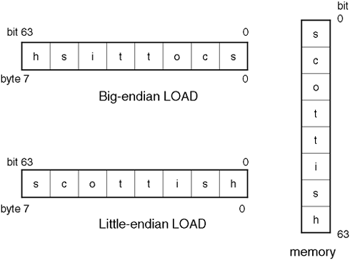
HISTORICAL NOTE: Endian relates to the way in which a computer architecture implements the ordering of bytes. In PA-RISC, we have the Processor Status Word (PSW), which has an optional E-bit that controls whether LOADS and STORES use big-endian or little-endian byte ordering. Big-endian describes a computer architecture in which, within a given multi-byte numeric representation, the most significant byte has the lowest address (the word is stored big-end-first). With little-endian, on the other hand, bytes at lower addresses have lower significance (the word is stored little end first).
Figure A-3 shows the difference between big-endian and little-endian byte ordering.
The terms big-endian and little-endian come via Jonathan Swift's 1726 book, Gulliver's Travels. Gulliver is shipwrecked and swims to the island of Lilliput (where everything is 1/12 of its normal size). There, he finds that Lilliput and its neighbor Belfescu have been at war for some time over the controversial material of how to eat hard-boiled eggs: big end first or little end first. It was in a paper entitled “On Holy Wars and a Plea for Peace” in 1980 that Danny Cohen used the terms big-endian and little-endian as a means by which to store data.
PA-RISC 1.x supported a style of 64-bit addressing known as segmented addressing. In this style, many of the benefits of 64-bit addressing were obtained without requiring the integer base to be larger than 32 bits. However, this did not easily provide the simplest programming model for single data objects (mapped files or arrays) larger than 4GB. Support for such objects calls for larger than 32-bit flat addressing, that is, pointers longer than 32 bits that can be the subject of larger than 32-bit indexing operations. PA-RISC 2.0 provides full 64-bit support with 64-bit registers and data paths. Most operations use 64-bit data operands and the architecture provides a flat 64-bit virtual address space.
One key feature of PA-RISC 2.0 is the extension the PA-RISC architecture to a word size of 64 bits for integers, physical addresses, and flat virtual addresses. This feature is necessary because 32-bit general registers and addresses with a maximum of 232 byte objects become limiters as physical memories larger than 4GB become practical. Some high-end applications already exceed the 4GB working set size. Table A-4 summarizes some of the PA-RISC 2.0 features that provide 64-bit support.
Table A-4. PA-RISC Features
New PA-RISC 2.0 Feature | Reason for Feature |
|---|---|
Provides 32-bit versus 64-bit pointers | |
Variable sized pages | More flexible intra-space management and fewer TLB entries |
Larger protection identifiers | More flexible protection regions |
More protection identifier registers | More efficient management of protection identifiers |
Load/store double (64 bits) | 64-bit memory access |
Branch long instruction | Increases branch range from plus or minus 256KBytes to plus or minus 8Mbytes |
[*] Processor state is encoded in a 64-bit register called the Processor Status Word (PSW). [†] The W-bit is bit number 12 in the PSW. Setting the W-bit to 0 indicates to the processor that data objects are 32 bits in size. Setting the W-bit to 1 indicates to the processor that data objects are 64 bits in size. The task of setting the W-bit is the job of the compiler/programmer. | |
Another PA-RISC 2.0 requirement is to maintain complete binary compatibility with PA-RISC 1.1. In other words, the binary representation of existing PA-RISC 1.1 software programs must run correctly on PA-RISC 2.0 processors. The transition to 64-bit architectures is unlike the previous 32-bit microprocessor transition that was driven by an application pull. By the time that technology enabled cost-effective 32-bit processors, many applications had already outgrown 16-bit size constraints and were coping with the 16-bit environment by awkward and inefficient means. With the 64-bit transition, fewer applications need the extra capabilities, and many applications will choose to forgo the transition. In many cases, due to cache memory effects, if an application does not need the extra capacities of a 64-bit architecture, it can achieve greater performance by remaining a 32-bit application. Yet 64-bit architectures are a necessity since some crucial applications, databases, and large-scale engineering programs, and the operating system itself need this extra capacity. Therefore, 32-bit applications are very important and must not be penalized when running on the 64-bit architecture; 32-bit applications remain a significant portion of the execution profile and should also benefit from the increased capabilities of the 64-bit architecture without being ported to a new environment. Of course, it is also a requirement to provide full performance for 64-bit applications and the extended capabilities that are enabled by a wider machine.
Another binary compatibility requirement in PA-RISC 2.0 is mixed-mode execution. This refers to the mixing of 32-bit and 64-bit applications or to the mixing of 32-bit and 64-bit data computations in a single application. In the transition from 32-bits to 64-bits, this ability is a key compatibility requirement and is fully supported by the new architecture. The W-bit in the Processor Status Word is changed from 0 (Narrow Mode) to 1 (Wide Mode) to enable the transition from 32-bit pointers to 64-bit pointers.
Providing significant performance enhancements is another requirement. This is especially true for new computing environments that will become common during the lifetime of PA-RISC 2.0. For example, the shift in the workloads of both technical and business computations to include an increasing amount of multimedia processing led to the Multimedia Acceleration eXtensions (MAX) that are part of the PA-RISC 2.0 architecture. (Previously, a subset of these multimedia instructions was included in an implementation of PA-RISC 1.1 architecture as implementation-specific features.) Table A-5 summarizes some of the PA-RISC 2.0 performance features.
Table A-5. The New PA-RISC Features
New PA-RISC 2.0 | Feature Reason for Feature |
|---|---|
Weakly ordered memory accesses | Enables higher performance memory systems |
Cache hint: Spatial locality | Prevents cache pollution when data has no reuse |
Cache line pre-fetch | Reduces cache miss penalty and pre-fetch penalty by disallowing TLB miss |
Because processor clock rates are increasing faster than main memory speeds, modern pipelined processors become more and more dependent upon caches to reduce the average latency of memory accesses. However, caches are effective only to the extent that they are able to anticipate the data, and consequently processors stall while waiting for the required data or instruction to be obtained from the much slower main memory.
The key to reducing such effects is to allow optimizing compilers to communicate what they know (or suspect) about a program's future behavior far enough in advance to eliminate or reduce the “surprise” penalties. PA-RISC 2.0 integrates a mechanism that supports encoding of cache prefetching opportunities in the instruction stream to permit significant reduction of these penalties.
A surprise also occurs when a conditional branch is mispredicted. In this case, even if the branch target is already in the cache, the falsely predicted instructions already in the pipeline must be discarded. In a typical high-speed superscalar processor, this might result in a lost opportunity to execute more than a dozen instructions.
PA-RISC 2.0 contains several features that help compilers signal future data and likely instruction needs to the hardware. An implementation may use this information to anticipate data needs or to predict branches more successfully, thus, avoiding the performance penalties.
When cache misses cannot be avoided, it is important to reduce the resultant latencies. The PA-RISC 1.x architecture specified that all loads and stores be performed in order, a characteristic known as strong ordering.
Future processors are expected to support multiple outstanding cache misses while simultaneously performing LOAD and STORE to lines already in the cache. In most cases, this effective reordering of LOAD and STORE causes no inconsistency and permits faster execution. The later model is known as weak ordering and is intended to become the default model in future machines.
Of course, strongly ordered variants of LOAD and STORE must be defined to handle contexts in which ordering must be preserved. This need for strong ordering is mainly related to synchronization among processors or with I/O activities.
As the popularity and pervasiveness of multiprocessor systems increases, the traditional PA-RISC model of I/O transfers to and from memory without cache coherence checks has become less advantageous. Multiprocessor systems require that processors support cache coherence protocols. By adding similar support to the I/O subsystem, the need to flush caches before and/or after each I/O transfer can be eliminated. As disk and network bandwidths increase, there is increasing motivation to move to such a cache coherent I/O model. The incremental impact on the processor is small and is supported in PA-RISC 2.0.
PA-RISC 2.0 contains a number of features that extend the arithmetic and logical capabilities of PA-RISC to support parallel operations on multiple 16-bit subunits of a 64-bit word. These operations are especially useful for manipulating video data, color pixels, and audio samples, particularly for data compression and decompression.
Let us move on to a reemerging design philosophy VLIW (Very Long Instruction Word). Intel and Hewlett-Packard have spearheaded its reemergence with their new IA-64 instruction set and Itanium and Itanium2 processors.
Table A-6 lists the features of Very Long Instruction Word (VLIW) architectures.
Table A-6. VLIW Architecture
Instruction Set Architecture (ISA) | Processor |
|---|---|
Intel IA-64 | Intel Itanium |
Multiflow Cydrome | Multiflow Trace Cydrome Cydra |
Characteristics of an VLIW Architecture | |
Fewer instructions | Large number of registers to maximize memory performance |
Very high level of instruction level parallelism | Multiple execution units to aid superscalar capabilities |
Uses software compilers to produce instruction streams suitable for superscalar operation | Less reliance on sophisticated branch management circuitry on-chip because the instruction stream by nature should be highly parallelized |
Fixed length instructions | |
The laws of quantum physics mean that the design philosophy of simply working harder by increasing clock speeds has a finite lifetime unless a completely new fabrication process and fabrication material is discovered. In the future, we are going to have to work smarter. A key to this is to try to achieve as much as possible in a single clock cycle. This is at the heart of any superscalar architecture. What we need for this to be accomplished is to have an instruction stream with a sufficient mix of instructions in order to activate the various functional units of the processor. Let's assume that our compiler is highly efficient at producing such an instruction stream. One way to further improve performance is to explicitly pass multiple instructions to the processor with every LOAD. We have to assume that any data required is already located in registers. What we now have with a single instruction is the explicit capability to activate multiple functional units simultaneously. One drawback with pure VLIW is that a program compiled on one architecture—for example, with two functional units, e.g., an ALU taking one cycle to execute an instruction and a floating-point unit taking two cycles to execute an instruction—will have an instruction stream taking into account these inherent limitations. If we were to move the program to a different architecture, e.g., with four functional units or possibly a faster floating-point unit, it would be necessary to recompile the entire program. The assumption I made earlier regarding data elements—“Any data required is already located in registers”—may also have an effect on the performance of the instruction stream. As processors evolve and increase in speed, memory latencies tend to increase as well; the disparity between processor and memory access times is one of the biggest problems for processor architects today. That assumption is based on the fact that pure VLIW provides no additional hardware to determine whether operands from previous computations are available; remember that it is the compiler's job to guarantee this by the proper scheduling of code. The result is that my assumption regarding data being already located in registers is no longer valid with pure VLIW. While VLIW offers great promise, some of its drawbacks need to be addressed. With clever design and the use of prediction, predicated instructions, and speculation, Itanium has endeavored to surmount all these drawbacks. They key benefits of Itanium can be summarized as follows:
Massively parallel instructions
Large register set
Advanced branch architecture
Register stack
Prediction
Speculative
LOADAdvanced floating point functionality
Intel and Hewlett-Packard jointly defined a new architecture technology called Explicitly Parallel Instruction Computing (EPIC), named for the ability of a compiler to extract maximum parallelism in source code and explicitly describe that parallelism to the hardware. The two companies also defined a new 64-bit instruction set architecture (ISA), based on EPIC technology; with the ISA, a compiler can expose, enhance, and exploit parallelism in a program and communicate it to the hardware. The ISA includes predication and speculation techniques, which address performance losses due to control flow and memory latency, as well as large register files, a register stack, and advanced branch architecture. The innovative approach of combining explicit parallelism with speculation and predication allows Itanium systems to progress well beyond the performance limitations of traditional architectures and to provide maximum headroom for the future.
The Itanium architecture was designed with the understanding that compatibility with PA-RISC and IA-32 is a key requirement. Significant effort was applied in the architectural definition to maximize scalability, performance, and architectural longevity. Additionally, 64-bit addressability was added to meet the increasing large memory requirements of data warehousing, e-business, and other high performance server and workstation applications.
At one point, the Itanium architecture was known as IA-64, to promote the compatibility with and extension of the IA-32 architecture. However, the official name as defined by Hewlett-Packard and Intel is the Itanium Architecture. It is said that Itanium is an instance of EPIC architecture.
In our discussion regarding VLIW, we noted that a key point of the architecture is the ability for the compiler to explicitly execute multiple instructions. To implement this idea, we no longer have individual instructions, but we have instruction syllables. In Itanium, we have three syllables that make up an instruction word or instruction bundle.
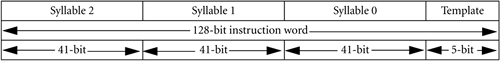
The instruction word is 128 bits in length. If life were simple, we would just glue together four 32-bit instructions and pass it to the processor. As we know, life isn't that simple. The 5-bit template determines which functional units are to be used by each syllable. Each syllable is 41 bits in length. One of the reasons to move away from a 32-bit instruction is the fact that almost every instruction in Itanium is executed by first checking the condition of a special register known as a predicate register. The first 6 bits of the instruction indicate which one of the 64 predicate registers is checked before execution is commenced. Architectural decisions such as predicate registers and branch registers allow compilers to do clever things when constructing an instruction stream, e.g., we can now compute the condition controlling a branch in advance of the branch itself. Itanium also incorporates branch prediction hardware, branch hints, and special branch hint instructions. This helps ensure that we minimize the rate of branch mis-predictions, which can waste not only clock cycles but also memory bandwidth. Altogether these features are designed to assist in constructing an instruction stream that is maximized for parallelism: work smarter. If we were to construct a block diagram of a VLIW instruction stream in a similar fashion to Figure A-2, it would look something like Figure A-4.
Some people would say that VLIW is using the best bits of both CISC and RISC. I can't disagree with such a statement, nor could I complain about it!
The question of which architecture is best is difficult to answer. As of December 2003, the Top 500 Web site (http://www.top500.org) listed the NEC SX-5 vector processor running at the Earth Simulator Center, in Yokohama, Japan, as the fastest supercomputer. It is, in fact, 640 8-processor nodes connected together via a 16GB/s inter-node interconnect. Building a single machine with that processing power (35.86 Teraflops) is too cost prohibitive for most organizations. The architectural design of such a solution is commonly referred to as a computational cluster or Cluster Of Workstations (COWs).
Just as an aside, we haven't mentioned vector processors simply because as a species, they are regarded as quite a specialized type of machine. A vector is a collection or list of data elements; think of a single-dimension array and you won't be too far off. A vector processor contains vector registers. When working on our vector of values, we have one vector in one vector register and another vector in another vector register. If our operation is an ADD the processor, it simply adds the contents of one vector to the other, storing the result in a third vector register. Such architectures can reap enormous performance improvements if a large proportion of your calculations involve vector manipulation. If not, the performance benefits may be negligible if any benefits are experienced at all. There is also an issue if your vector isn't the same size as the vector register. The processor has to go through a process of strip mining whereby it loops through a portion or part of your vector, performing the operation on each part until it is finished. Many people regard vector processors as too focused on a particular class of problem, making them not applicable in general problem solving scenarios. The truth is that many architectures these days are including vector registers as part of the architecture of their register sets in an attempt to try to appeal to a class of problems that can utilize vector processing.
To answer the question at the top of this section—“which architecture is best?”—the answer as always is “it depends.” The architectures we have looked at here, including vector processors, span the majority of the history of computing. As ever-demanding customers, we expect our hardware vendors to be constantly looking to improve and innovate the way they tackle the problem of getting the most out of every processor cycle.
My original intention was to look at some techniques that system architects use to focus on the third point of the work ethics in order to get the most out of time … get someone else to help you. On reflection, I feel that we should take a look at “memory” in detail. Our discussions surrounding multi-processor machines will be affected by a discussion regarding memory, so let's start there.
The ideal scenario for storing data is to store all the data we are currently using in registers. They are the quickest form of memory storage in a computer. Unfortunately, cost, volatility, space, power requirements, and heat dissipation all inhibit the likelihood of a processor ever existing that accommodate all the data we are currently using. Consequently, we need some other form of storage to keep our data. The closer we are physically located to the processor, the better the performance, but at ever increasing cost. Figure A-5 shows this memory or storage hierarchy.
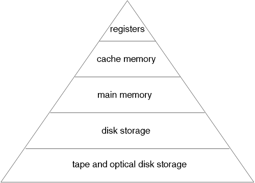
Our memory hierarchy is trying to alleviate the problem of not having enough storage capacity on the processor itself. The solutions we have available to us at present include using high-speed memory (a.k.a. cache memory) is the best solution. The crème de la crème of cache memory is a cache that we can access in one clock cycle. Such a low latency will probably require that the cache is physically located on the processor die itself. In turn, this will limit the size of this Level 1 (L1) cache possibly to tens of kilobytes, but in some cases a L1 cache in the megabyte range has been seen. Cache memory is made up of SRAM (Static Random Access Memory) chips. They differ in a number of ways to the chips used for main memory. Main memory is made of a type of memory chip known as DRAM (Dynamic Random Access Memory). The Static in SRAM relates to the state of a memory cell while power is applied to the device. Memory cells in a SRAM chip will maintain their current state, i.e., hold their current data item, with no further intervention. The Dynamic in DRAM requires the memory cells to be acted upon in order for them to retain their current state. DRAM chips are comprised of MOS (metal oxide semiconductor) devices that have high densities and are relatively cheap to fabricate. The drawback is that they use a charge stored in a capacitance to indicate their state: on or off. Unfortunately, this capacitance can drain away if left unchecked. A DRAM cell would lose its charge and therefore lose the data stored in it. DRAM chips need to be refreshed (read, then rewritten) usually every millisecond or two to ensure that the data held in a memory cell is maintained. While this refresh is being performed, the data in a DRAM cell cannot be accessed. SRAM chips are similar to processor registers: They are effectively an extension of the electronic bistable flip-flop. One benefit of these electronic latches is that the charge is static and does not need refreshing. Another benefit is due to their similar nature to registers; we can access them in one clock cycle if they are located sufficiently close to other processor elements. SRAM chips are faster than DRAM, but unfortunately considerably more expensive—usually a factor of 10-20 times more expensive. There are few computers that have all memory made of SRAM chips; CRAY supercomputers are the main exception. Seymour Cray famously once said about the dilemma between using SRAM chips in preference to DRAM chips irrespective of cost, “You can't fake what you don't have.” Before looking at cache architecture, let's look at some figures related to access times for memory in relation to processor speeds. Let's take a fictitious processor operating at 500MHz:
A clock tick occurs every 2 nanoseconds. The ideal is to execute an instruction every clock tick. Typical DRAM access times are in the order of 60 nanoseconds. Some chip manufactures are trying to bring that speed down with technologies such as SDRAM (synchronous DRAM), Rambus, and EDO (Extended Data Out) memory. These technologies are still essentially DRAM chips but with additional technology in order to improve access times in respect of SRAM memory. In essence, for every memory access we could execute 30 machine instructions. This is the major reason we need high-speed memory—SRAM—in order to alleviate some of that imbalance. In fact, studies have shown that somewhere around 30 percent of instructions make reference to memory locations (in RISC, that would mean 30 percent of instructions are LOAD/STORE instructions). Operating systems commonly use Virtual Addresses to access memory, meaning that every memory reference is now a reference to a virtual address, be that a reference to the next instruction or to a data element. This is an additional task for the processor to perform. Many modern processors use a special Functional Unit known as the TLB (Translation Lookaside Buffer). For our simple example, we won't use a hardware TLB; rather, we'll require the processor to perform the translation itself. The result is that is that every memory reference equates to:
1reference_ for_ an_ instruction + (1reference _for_ data*30%)=1.3 virtual_ address_ references
Take into account that every memory reference occurs in two stages: (1) perform the Virtual to Physical translation, and then (2) fetch the datum from the Physical memory location. This means that with no assistance from a TLB, every memory reference is in fact making 2.6 real memory references. With our fictitious processor running at 30 times faster than our DRAM chips, the processor is consistently 2.6 x 30 = 61.8 times ahead of memory as far as access times are concerned. The natural response to this is that we need memory to operate at a faster speed. In fact, with a superscalar and super-pipelined processor, it can be argued that memory needs to operate faster than the processor. This would mean that we would need to invent an electronic device that can react quicker than a register. If someone invented such a device, I can guarantee that the first architects to use it would be the processor architects themselves, and we would get into a circular argument regarding processor and memory speeds. Our best effort is to use devices that can react as quickly as a register. Today, that means SRAM.
Let's first look at SRAM cache chips. Due to their cost, SRAM memory chips are smaller in capacity than their main memory counterparts. Being located close to the processor also limits their size. All of these size limitations don't seem to bode well for the performance of cache memory. As we see, the nature of how programs function means that having a small amount of cache memory doesn't hinder performance as much as we first think. It is seldom that we have a program that is purely sequential in flow, i.e., we start with the first instruction, move on to the next, and simply step through instruction after instruction until we get to the end. A typical program will have some form of repetition built into it, some form of looping construct whereby we work on a given set of instructions and possibly a similar set of data in a repetitive manner. This highlights a concept know as the principle of locality. Basically, there are two types of locality:
Spatial locality: Spatial locality deals with the notion that the data we are about to access is probably close to the data we have just accessed, i.e., the next instruction in our loop is close to the last instruction. Logically, this seems to make sense.
Temporal locality: Temporal locality deals with the concept that once we have accessed a piece of data, there is a strong probability that we will access the same piece of data in the not-to-distant future. Again, our notion of looping in a program means that we come around to the same instructions in the not-so-distant future. Again, logically this seems to make sense.
Considering both Spatial and Temporal locality, the prospect of having a relatively small but very fast cache is less of an impact than maybe we first thought. The chances are good that data and instructions will be in the cache the next time we need them. If we remember back to the von Neumann principle where data and instructions are both considered simply as a stream of data, we could see an immediate bottleneck in the design of our cache. We can be accessing the cache only to retrieve either a data element or an instruction, but not both simultaneously, i.e., the von Neumann bottleneck. Then we consider the principle of a superscalar architecture where we can be activating separate processor components as long as they are involved in separate tasks. The resulting technology is simple and elegant: Implement a separate cache for instructions and a separate cache for data. This means utilizing a separate instruction and data cache as well as a separate bus into the processor for each cache, effectively doubling the overall datum bandwidth into the processor. An architecture that utilizes separate data and instruction memories is known as a Harvard architecture. Today, it is used to identify architectures with separate instruction and data caches, even though main memory instructions and data are stored together, i.e., monolithic. Most high performance processors have a separate instruction cache (I-cache) and data cache (D-cache). Next, we look at how cache is organized. The cache architecture employs circuitry designed to decode a memory address to one of a number of cache lines. A cache line is a number of SRAM cells whose size is the unit of transfer from cache to main memory. This is to say that if we LOAD a 64KB cache line, we will transfer 64KB worth of data/instruction, even if we only asked for 2KB. This buffering can be a benefit to performance. If we think back to the notion of Spatial locality, this concept dictates that the next piece of data we require will be located close to the location of the current data element. If we have recently transferred too much data for the original request, there is a high probability that the data we now require is already in cache. The same ideas apply to the notion of Temporal locality and apply to both instructions and to data. A difficult question to answer is the ideal size for a cache line. If it is too large, we will need to perform large transfers to and from main memory. Performing large transfers from cache to main memory is going to impose the same transfer-time problems that we documented between processors and main memory. The size of the cache line is a decision for the processor architects. The design of the instruction set will uncover an ideal size for instructions. For data elements, they may use historical data to try to establish a “typical” data flow for such a processor and try to match as close as possible the cache line size to it. In reality, a general-purpose computer will not have a typical data flow for this type of processor. Ultimately, it is up to programmers to establish what the designer has chosen as the cache line size. With this and other information, the programmer needs to model his or her application data accordingly. The programmer will be trying to avoid a situation known as cache thrashing. Cache thrashing is where a program is continuously referencing a particular line in the cache simply as a consequence of the design of the data model used in the application. Consequently, we need to flush or purge the cache line every time a new datum needs to be loaded. Because this requires writes to and reads from main memory, programmers should try to avoid this as much as possible. The main reasons for cache thrashing is an unexpected conflict between cache organization and the data model used in the application. Programmers should be aware of the principle of locality as well as how the cache is organized on the systems that will run their applications and construct their data model with both of these in mind. It is not only the cache line size the programmer will need to consider when constructing his data model, but also the way that a memory addresses map onto cache lines. This is known as a mapping function used by the cache logic circuitry.
There are three ways we can organize cache mapping:
Direct Mapping: This is where only one cache line maps to a given block of memory addresses.
Fully Associative: This is where any cache line can map to any block of memory addresses.
Set Associative: This is a mapping where there are a number of cache lines that map to a given block of memory addresses.
Before we look at each mapping, we look at a basic processor where some basic design criteria have already been established:
The cache has only eight cache lines.
Each cache line holds four bytes.
This means that we need three bits to identify a specific cache line (23 = 8 cache lines) and two bits to identify an individual byte within a cache line. This is known as the offset (22 = 4 bytes of an offset). The rest of the address will be used as an identifier or tag field to ensure that the cache line we are interested in currently has our data element. With 3 bits being used to identify the cache line and two bits to represent the offset, our tag field will be three bits in size.
Let's look at some examples of each of these cache mappings in order to fully understand how each works, as well as the costs and benefits.
With a direct mapped cache, a particular memory address will always map to the same cache line. The cache logic to employ such a design is the most simplistic of the mapping functions and is hence the cheapest. It has drawbacks in that a number of memory addresses might get decoded to the same cache line. This can lead to the situation known as cache thrashing, which basically means that we have to get rid of old data to make way for new data. If both data elements are in constant use, we could have the situation where two pieces of data are in effect consuming the entire bandwidth of the cache. In such a situation, we get what is known as cache hot spots. Let's look at how direct mapping works.
NOTE: It is common to represent binary information in hexadecimal: Writing a 64-bit address in binary can be somewhat cumbersome. Using hex means that we can represent an 8-bit byte with just two hex digits. I use both forms in the accompanying diagrams where appropriate.
Figure A-6 represents the direct mapping of our 16-bit address to a cache line.
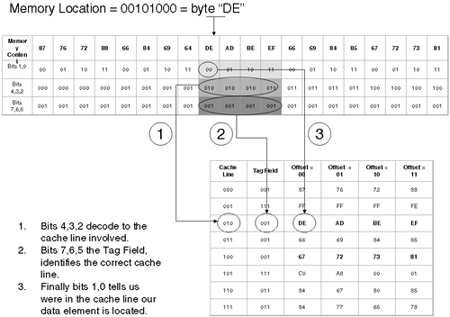
The problem we have here is that if the next datum we access happens to be at address 01001000 (notice that only bits 5 and 6 have changed), we have de-referenced to the same cache line. We will have to write the current cache line to memory before moving our new datum into cache, and that's a time-consuming and lengthy process. It transpires that, in our architecture, after every 32 bytes we hit this problem of decoding an address to the same cache line. A multiple of 32 bytes can be seen to hit upon our cache hot spot. A programmer would have to be aware of how the cache was organized, as well as the number and size of cache lines before designing his data model. As you can imagine, the overall performance of an application will be seriously affected if the data model happens to discover a cache hot spot.
This mapping scheme is at the other end of the spectrum of cache organization in comparison to a Direct Mapped cache. In this design, any memory reference can be stored in any cache line. A number of issues arise out of this design.
Do we need to use some of the address bits to encode a cache line number?
The answer to this question is no. Because an address can decode to any line, a single cache line is of no relevance to a particular memory address.
The issue of Temporal locality needs to be addressed in that we would prefer not to remove a data element that is likely to be reused in the near future. We discuss replacement strategies after talking about Set Associative mapping. It is enough to say that it is desirable to record the frequency with which a cache line has been used.
A Fully Associative mapping will use more bits to identify whether a cache line contains our datum. In our example, we can disregard bits 2 through 4 encoding a cache line and, hence, our tag field now uses bits 2 through 7 as an identifier. Drawbacks of this mapping scheme include the fact that we need to ensure that a lookup of a cache line is very rapid. Every memory reference could require us to look up every cache line and compare bits 2 through 7 of the tag field with the corresponding bits in our memory reference. This makes Fully Associative mappings more expensive to employ. Figure A-7 shows an example mapping.
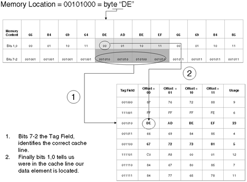
On one hand, we have a simple, cheap but effective mapping scheme with a Direct Mapping. On the other hand, you have this sophisticated, expensive solution with Fully Associative Mapping. Set Associative Mapping sits in the middle: It tries to avoid the cache hot spot problem of Direct Mapping, but the cache logic is not as complicated and, hence, it is cheaper to employ than Fully Associative Mapping. The idea with Set Associative Mapping is that we will construct a Set of lines that can accommodate our memory reference. Any one of the lines in this Set can accommodate a given memory address. This avoids the cache hot spot problem of Direct Mapping. What we need to do is to change the logic of how the decoding of a memory address works. Instead of decoding to a single cache line, the memory address will decide a set of two, four, or possibly eight lines. In our simple example, we have eight cache lines. If you look at the binary representation of a cache line number, you might notice that we get a form of repetition in the binary notation, 010 and 110 for instance: The first two bits of the cache line are same, i.e., 10. We can use this as our encoding scheme. We will use part of the memory address to encode to “line 10”. In our case, this will decode to two possible line numbers. We will use the remaining 4 bits as our Tag Field as before: to verify that the data in the cache line is actually our data. This is an example of a two-way Set Associative Mapping: two cache lines for the Set of cache lines in which my data can reside. Depending on the design of our cache, we can have an n-way Set Associative Mapping where each Set will contain n lines. When we come to place our datum in the cache line, both lines may already be occupied. The cache logic will have to make a decision as to which line to replace, and it may be prudent to use a Usage Field as we did in the Fully Associative Mapping in order to maximize the benefits of the principles of locality.
Figure A-8 shows an example of our two-way Set Associative Mapping.
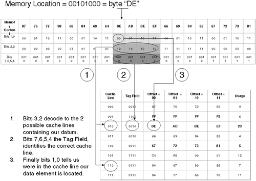
The choice of cache mapping used is a design decision for the processor architect: speed but complexity with Fully Associative, simple but prone to cache hot spots with Direct Mapping, or the compromise choice of Set Associative. If either Fully Associative Mapping or Set Associative Mapping is used, the architect will have to take into account the idea of the Usage Field and how it should be interpreted. Let's discuss replacement strategies in the context of cache lines where we are using an Associative Mapping.
When we come across a situation where we need to replace a cache line with new data, we need some policy for choosing which cache line to select. It is possible to adopt a random policy, and statistically we would choose the best cache line a fair proportion of the time. Conversely, statistically we could choose the worst line a fair proportion of the time as well. Instead of leaving it to chance, we could employ some intelligence into the decision as to which cache line to choose to replace. When we consider our principles of locality, it would be advantageous to choose a cache line that is least likely to be needed in the near future. In this way, we are avoiding the laborious process of having to write back data to main memory only for it to be read back in again in the near future. The concept of a Usage Field is common in order to choose the most appropriate line. The Usage Field will track how often a cache line is accessed. There are essentially three choices of replacement strategies.
Last In First Out (LIFO)
We will not spend much time considering this replacement policy. LIFO means that the newest datum to be brought into cache is the first one to be replaced. When we consider Temporal locality, it is likely that we will probably need the newest datum in the near future. Immediately getting rid of it flies in the face of the notion of Temporal locality. We are encouraged in this assertion by the fact that no cache in production uses this replacement strategy.
First In First Out (FIFO)
The idea here is that the oldest member of the cache is the first line to be replaced. The logic dictates that each datum should be allowed a fair amount of time in cache without a single datum dominating the cache entirely. The contradiction is that if a line is still in use, there is little reason to replace it. In fact, in many ways you could argue that if a cache line has been resident for a long time, then getting rid of it may mean that you are getting rid of the most heavily utilized datum. Both of these arguments are missing one crucial ingredient: They do not take into account when the cache line was last used.
Least Recently Used (LRU)
Least Recently Used attempts to overcome the problem of FIFO by taking into account when a cache line was last used. It requires the cache logic to record in some way aspects of the usage of the cache line. This in itself can be a complicated process. This complexity is mitigated by the fact that we are building significant intelligence into the replacement strategy. We will choose a line that has been least used with respect to some timeframe. The principle of Temporal locality reinforces this: If we are using a datum, we will probably need it again soon. The fact that we haven't needed that datum recently probably means that we will not need it in the near future either. Regardless of its complexity and inherent cost, LRU has been seen to be the most popular with processor architects.
There are a couple of other items I want to deal with before leaving the topic of cache.
Multiple levels of cache
When we write from cache to memory
As we demonstrated earlier, the speed differential between a processor and memory is alarmingly high. We have tried to alleviate this problem by employing a cache. The dilemma we now have is how big to make that cache. In an ideal world, it would be big enough to satisfy a program's locality of reference. On a real computer system with hundreds of programs, the size of this locale can be vast. The result is that our L1 cache is likely to be relatively small due to speed requirements; it needs to be physically close to the processor. In order to further alleviate the problem of having to access main memory, we could employ a second level (L2) cache. This is often off-chip but relatively close to each processor module. Access times will be somewhere between the L1 cache and main memory. Being off-chip and slightly slower than the L1 cache means that the cost will be reduced.
We need to mention one last topic in relation to cache behavior: the topic of writing from cache back to memory. When a cache line is modified, when does that change get stored back to main memory? If we were to immediately write that change to memory, we would incur the penalty of the time it takes to perform a transfer to memory. The positive aspects of this policy are that we know that our cache and main memory are in sync. This policy is known as write-through.
The alternative is a write-back policy. This policy will write the datum back to memory only when the cache line needs to be used by another datum. This has the advantage that if a datum is being modified frequently, we eliminate the costly additional writes to memory that a write-through policy would require. One cost to this design is that we need to monitor when a cache line has been modified. This can take the form of a dirty bit being set for a cache line, indicating that a change has been made (subsequent changes don't need to update the dirty bit because once it is set to true, we know that at least one change has been made). Another cost of a write back policy is when an instruction needs to update a datum that is not currently in cache. The normal mode of operation with a write back policy is to first fetch the datum into cache and then modify it: The reason for this is due the principle of Temporal locality. With a write-through policy, Temporal locality still applies, but this policy dictates that every write to cache initiates a subsequent write to memory. In many cases, the fetch of the datum into cache is not carried out; we will simply schedule the update of the datum at the prescribed main memory address some time later.
We have discussed at length the performance of SRAM in relation to DRAM. Main memory is a collection of DRAM cells. If we were to draw a simple diagram of the relationship between processor, cache, and memory, it would look something like Figure A-9.
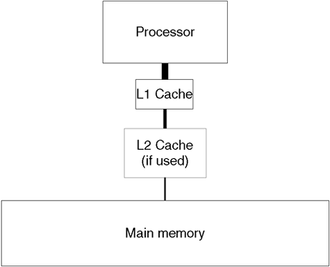
With both instructions and data being stored in main memory, we will come to a point where pipelined instructions need to access memory. Were we to have a single pool of memory as in Figure A-9, we would quickly come across memory contention where both data and instructions are trying to be fetched via the same datum path. The result would be that our pipeline would stall for longer than we would like. One solution is to split the pool of memory into multiple blocks of memory with independent paths. This is a common practice because it is not overly expensive and we have increased the overall memory bandwidth by providing multiple locations to store instructions and data. The blocks of memory are known as memory banks and the process of using each bank simultaneously is known as interleaving. The idea here is that when the memory subsystem (circuitry between the cache and memory) needs to transfer a cache line from main memory, it will go to a specific memory bank to retrieve it. Loading the very next cache line will require the memory subsystem to go to the very next memory bank; hence, we interleave between memory banks and reduce the overall access time by avoiding memory contention. Figure A-10 shows a memory subsystem with four memory banks (we have left off an L2 cache for simplicity).
The reason we have gone to the level of detail of showing you memory banks and the cache line size is to reiterate the importance that programmers can have on our overall system performance. Let's assume that we have data elements of varying size, but they are all a multiple of the word size that is 32 bytes. In a single cache line, we can accommodate eight words. Our program has used a structure or array to store these data elements. Unfortunately, two things have conspired against us: first, the design of our structure/array is like this:
struct employee{
name; (= 3 words)
employee_number; (=1 word)
age; (=1word)
address; ( =6 words)
marital_status; (=1 word)
job_code; (=2 words)
job_title; (=3 words)
job_location; (=3 words)
deparment; (=2 words)
manager; (=3 words)
performance_rank; (=3 words)
salary; (=2 words)
salary_bank_sortcode; (=2 words)
salary_bank_account; (=2 words)
social_security_number; (=2 words)
};
We will assume that storage of these data elements is sequential in memory and we can pack words together one after another. In total, we have a structure that is 32 words in size. The second thing conspiring against us is that we have four memory banks. If we were to load an entire employee structure from memory, it would take up four cache lines. Suppose that we wanted look up all employee numbers: The employee_number is stored in cache line 1, 5, 9, and so on. It so happens that data access patterns like this highlight is what is known as bank contention. Every access to a subsequent employee_number means that we are fetching the next data item for the same memory bank. In this way, we are not utilizing the benefits that interleaving had promised us. We would need to instigate a detailed study to uncover whether this form of access pattern was common. If so, we would have to modify our data model to alleviate it; we would need to employ further empirical studies to measure the response times of our applications under varying workloads and varying data models before making a decision on how to reengineer our application—a task that most people are not willing to undertake.
We couldn't go any further with our discussion on processors without mentioning virtual memory. Processes are given a view of memory that makes them think they have access to every addressable memory reference: In a 64-bit architecture, this means that a process has access to 16EB. This isn't really the case. Each process uses Virtual Addresses to access their data and instructions. This is commonly known as a VAS: a Virtual Address Space. The operating system will maintain a Global Address Space, which is essentially a mapping of all of the VASes available and which process is using which one. The advantage of using Virtual Addresses it that processes have no concept of the actual memory hierarchy used at a hardware level, allowing programs to be moved from machine to machine with no regard for the underlying hardware memory interface. The operating system, i.e., the kernel, is the interface to hardware and as such has to maintain some form of list of which Virtual Addresses actually relate to pages of data located in Physical memory. This list of active pages is commonly referred to as the Page directory. In the context of this discussion, when a process is executing, it is using its Virtual Addresses to access data and instructions. Every memory reference will require the operating system to translate that Virtual Address to a real Physical Address. If the Page Directory itself is stored in memory, we have all the access time issues we have discussed previously with main memory. One solution is to maintain a cache of address translations in a special hardware cache known as the TLB (Translation Lookaside Buffer). The use and success of a hardware TLB again highlights the importance of the principles of locality. If we are using a piece of code now, we will probably need it again soon: That's temporal locality. It is also likely that the next piece we need will be relatively close to where we are now: That's spatial locality. This all lends weight to the argument of utilizing a hardware TLB. This is reflected in the fact that lots of processors utilize a hardware TLB. Being on-chip, as in the case of an L1 cache, the size of a TLB is limited. If we can't find a translation in the TLB, we have suffered a TLB miss. This needs to be rectified by fetching the translation from the main memory Page Directory, potentially wasting overall execution time. To alleviate this problem, we again need to look at our programs and how they are effectively using the TLB. We saw earlier that main memory is a collection of pages: On HP machines, that's a page 4KB in size. Programmers need to be very careful how they construct their data models and how subsequent data elements are referenced. If two frequently accessed data elements are more than 4KB apart, we will see two entries in the TLB. When accessing multiple pairs of data elements, this can lead to the TLB becoming full. Subsequent TLB references invoke a TLB miss and delays in ensuring that the TLB is updated appropriately. It is an unfortunate consequence of the programs we use that they utilize features such as multi-dimensional arrays and, from C programming, structures: This can be thought of as a record where we group together data elements that have some collective meaning, e.g., the name, address, and employee number would form an employee record or employee structure. We could ask our programmers to look again at their data model in lieu of the fact that we now know the issues dealing with page size, cache size, and memory access times. This is a lengthy process and needs to be thought out very carefully. One other solution is to fundamentally change the way our machines view memory. With bigger pages, it means that our big data structures will fit in fewer pages. Fewer pages means fewer TLB references, which in turn means fewer chances of a TLB miss and the associated costs in memory accesses. For HP-UX, this has become an option with the advent of the PA-8000 processor. What we can do is to change the effective page size on a program-by-program basis. This will gives us the effect described above: fewer pages meaning fewer TLB references. Some people think this is such an easy fix that we should apply this to all programs. This is not necessarily the case. If we have a small program, e.g., one of the many daemon processes we see on UNIX, and we set the page size at 1MB, that process will be allocated pages of memory in multiples of 1MB when it needs only a few KBs. This can lead to a significant waste of memory. Utilizing the idea of Variable Page Sizes needs to be done judicially and with an understanding of the underlying data access patterns. In Chapter 11, “Processes, Threads, and Bottlenecks,” we discuss how we can instigate this change to a program whereby we can change the size of text as well as data pages.
We have seen that simply working harder is no longer the only choice available to us. The laws of physics mean that time is running out on simply working harder. We have looked at some ideas on how processor designers are trying to work smarter in order to extract as much from a single CPU cycle as possible. We have discussed some of the prevalent architectures available today and how they try to work smarter. We have also discussed cache memory as well as main memory. Applications nowadays require so much processing power that it is unrealistic to find a machine with a single processor capable of the task. Economic forecasting, fluid dynamics, and digital image processing all manipulate vast amounts of data and in many cases demand output in real time. To provide this level of performance, we need to harness the power of multiple processors in order to provide the performance bandwidth required. This can be achieved in a number of ways: everything from interconnecting individual processors in a large array-like configuration to harnessing multiple computers themselves, interconnected by a high speed, dedicated network. A level of concurrency in our architecture can lead to dramatic improvements in overall throughput. Our first task is to try to classify the myriad design decisions into a manageable classification scheme. In this way, we categorize what we are trying to achieve and compare that with the characteristics of competing architectures. A convenient and well-used method to study these concepts goes back to 1972 and uses Michael Flynn's Classification.
In 1972, Michael Flynn designed a classification system to encapsulate the differing computer architectures attempting some level of concurrency in operation. To this day, Flynn's Classification is a well-used and convenient way to study concurrency. Its beauty lies in its simplicity. Flynn categorized features in concurrency by noting that concurrency happens in one of two places. We can achieve concurrency when working on data and/or instructions: A computer can work on a single or multiple instructions. Similarly, a computer can work on a single data element or multiple data elements. With such a simple philosophy, we end up with four basic models to study.
The PC on which I'm writing this book is an SISD machine. Here, we have a control unit fetching and decoding instructions from some form of memory. This single instruction stream is passed to the processor to execute. As we have seen, most processors have this control unit as part of the processor hardware itself. Any data that the processor needs will come from the memory system via a single data stream. This is the traditional von Neumann machine (see Figure A-11).
In this design, we still have a single instruction stream. The Controller transmits this instruction to all the processors. The processors themselves will have some local memory to store data elements that they will retrieve from some memory system. When instructed by the Controller, all processors execute the single instruction on their own data elements. In its purest form, it's hard to see how a processor will communicate directly with the memory system to access its own data elements. A common feature of SIMD machines is that a host computer provides a user interface and storage, and supplies data elements directly to the individual Processors. The Controller has its own control processor and control memory. A large proportion of the control operations of the executing program will be performed by the Controller. The Controller will call on the processors to perform arithmetic and logical operations only when necessary. Where we have large collections of data elements and want to perform the same operation on all data points, e.g., vector or array manipulation, such an approach may be appropriate. SIMD machines have been seen to be too specialized in their approach to problem solving and have consequently gone slightly out of favor. Machines such as CRAY and Thinking Machine supercomputers are SIMD machines. Their specialized approach to problem solving lends them to particular classes of problems, e.g., forecasting and simulations where manipulation of large collections of data is central to the types of problems encountered.
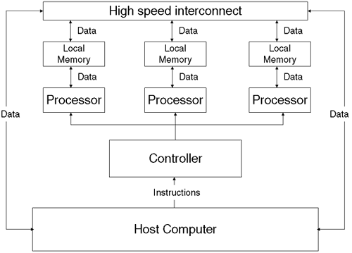
This type of machine is not common because we have multiple processors issuing different instructions on the same data. Flynn had trouble himself visualizing this. One example commonly cited is characterized by machines used in complex mathematics such as cracking security codes. Each processor is given the same data (cyphertext). Each processor works on the same data by trying different encryption keys to break the code. In this way, we would be achieving concurrency by having the set of possible keys divided by the number of processors.
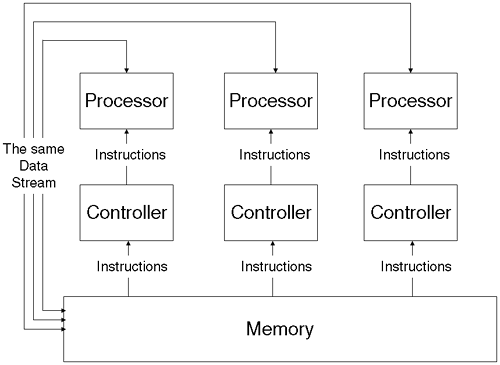
These are the most common concurrent machines you will find in the workplace. This type of machine forms the cornerstone of multiprocessing as we know it. Each processor issues its own instructions delivered by its own controller and operates on its own data. Processors can communicate with each other via the Shared Memory Pool or via some primitive messaging system. Within this classification, you will find variants such as Symmetrical Multi-Processing (SMP), Non-Uniform Memory Access (NUMA and its variants, e.g., cc-NUMA, NORMA), and Collection Of Workstations (COWs). Machines that house processors and memory in a single chassis are known as tightly coupled, whereas machines where collections of processors and memory are housed in separate chassis are known as loosely coupled.
Because this type of machine is the most common in the marketplace, we look a little closer at some of the variants we find with the MIMD classification, namely SMP and NUMA (see Figure A-14).
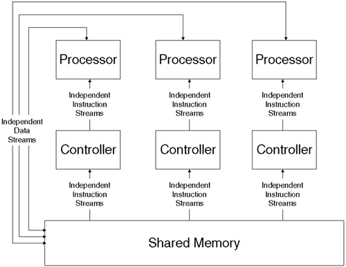
Figure A-14. MIMD machine using Shared Memory as a means by which processors communicate with each other
This architecture is best described by describing the symmetry hinted at in the title. The symmetry comes from the notion that all processors have equal access to main memory and the IO subsystem in terms of priority and access time. This also means that the operating system as well as user processes can run on any processor. Older attempts at SMP failed this last test:
Master/Slave: This is where one processor is dedicated to running the operating system: the master. All other processors were used for user processors.
Asymmetric: This allows the operating system to run on any processor, but only one processor.
Both these implementations have serious limitations. In a system that is performs lots of IO, all IO interrupts coming from the external and internal devices will be handled solely by the master or monarch processor. Without distributing IO interrupts, the monarch could be swamped with processing requests leaving the user processors waiting for IO events to be acknowledged, letting them continue with their computations. HP-UX still has the concept of a monarch processor, but only to boot HP-UX. Once booted, all processors are treated as equal.
A simplified diagram of this an SMP can be seen in Figure A-15.
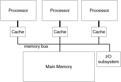
It may seem a trivial exercise to extend this architecture to accommodate an infinite number of processors. If you recall during our discussion on memory, we found that a uni-processor machine can quite simply swamp a DRAM-based memory system. The solution was to employ SRAM cache. The size of our cache is one aspect of our SMP design that will be crucial as to whether our SMP architecture will scale well. What we mean by this is that by adding additional processors, our overall system performance should scale proportionally. If we add a second processor, all else considered, we would expect a 100 percent improvement in performance. To avoid too much memory contention, we need to look at two aspects of this design:
Cache size
Memory bus interface
We have discussed cache performance previously. The increased cost of providing a significant amount of L1 SRAM-based cache means that a hardware vendor needs to feel confident that its customers will pay the price. A single L1 cache architecture may be used in both uni-processor and multi-processor models. Many database systems work on many megabytes of data and, hence, their Spatial locality is large. These and other similar applications will benefit from larger caches. The second aspect of SMP design that we need to consider is the architecture of the memory bus. In its simplest form, it is a collection of wires that pass information between the processor(s) and the memory subsystem. The number and bandwidth of each data path will influence the overall scalability of the SMP design. Having a single, large memory bus will require some forward thinking; we will need to think of the largest SMP configuration that we will ever support, add to that the maximum expected bandwidth required per processor, and multiply these figures together to give us a maximum peak bandwidth requirement. This would probably require additional wires connected to each processor. Additional wires are expensive and require additional pins on the processor to be available. With all the other resources requiring access to the processor, this can be a limiting factor in this overall design. If we cannot provide the required bandwidth, our processors will stall due to cache line misses and the latency in fetching datum into cache. As mentioned previously, overall cache size can alleviate this as can the size of each cache line. Another method to improve overall scalability is to have sufficient connectivity to allow every processor independent access to every memory bank. If we have multiple non-conflicting requests, they can all be satisfied simultaneously. Such a design is often referred to as a crossbar architecture. The interconnection of wires is managed by some clever circuitry that deals with arbitrating among conflicting requests. This arbiter is commonly known as a crossbar switch. Figure A-16 shows diagrammatically how a crossbar switch may look.
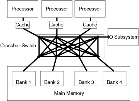
As you can see, the scalability of such a solution is intrinsically linked to the ability to scale the connectivity within the crossbar switch. If we were to double the number of processors, we would quadruple the number of connections within the crossbar switch; in fact, increasing the number of processors by n increases the number of connections by n2. Although vendors such as HP have supplied this architecture in the V-Class machines, the cost of supplying significant scalability is the limiting factor in whether such a design will succeed. Before moving on to look at NUMA architectures, we need to look at how a number of caches will operate when functioning in a multiprocessor architecture.
As we mentioned previously, a common policy employed in a cache for writing data to memory is known as write back; this means that data will stay in-cache until that cache line needs to be freed for some other data. In a multi-processor model, this becomes more complicated. What would happen if one processor required data that currently resides in the cache of another processor? Some people would think this unlikely. Consider the case where multiple threads are executing on separate processors (processor 1 running thread 1 and processor 2 running thread 2). It is not unreasonable to assume that in some cases threads from the same process could require access to the same data. How does processor 2 get the data from the cache of processor 1? We could build into the operating system a low-level instruction that checked all the caches for the datum required, and if we found it, it would then manage how the data would get transferred to processor 2. Due to the overheads involved, very few architectures employ software cache coherency. What is required is some mechanism by which the hardware can manage this. There are a number of hardware solutions to cache coherency. The most common are:
A snoop bus
Directory-based cache coherency
The idea of a snoop bus is to provide a mechanism for caches to snoop on each other. If processor 1 requests a cache line, it will make that request via a broadcast to all other processors and to the memory subsystem. If the cache line is currently residing in another processor, that processor will transfer the cache line to processor 1 and signal to the memory subsystem that the request has been met. To provide this, we would have to utilize existing bandwidth within the memory bus itself to communicate cache coherency between processors. This does not scale well with the memory bus quickly becoming overwhelmed by the additional traffic; the broadcast is going to have to wait until the bus is free before sending the broadcast (known as bus arbitration). One solution would be to provide a private, separate snoop bus that processors and the memory subsystem could use uniquely for snooping. Figure A-17 shows such a configuration.
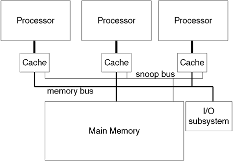
This design works well, but again we need to consider the problem of scaling. If we want to support large SMP configurations, we need to consider how much additional workload cache coherency will impose on the processor infrastructure; more and more processors increase proportionally the likelihood that we will be requested to transfer cache lines to other processors. If we could infinitely increase the bandwidth of the snoop bus and maintain latency times to satisfy each additional request, this design might work. The costs of increasing the snoop bus have put realistic limits on the scalability of this design. The snoop bus (whether private or as a function of the memory bus) still has many supporters in the processor industry, even though it has been found by various hardware vendors that, above approximately 20 processors, this design may need some careful designing.
This design also requires additional hardware. It is more complex and more expensive; however, it has been shown to scale better than a purely snoop bus. In this solution, we have a hardware directory that is hardwired to all the caches; you could imagine it as building extra intelligence into our crossbar design. We might even have an independent snooping crossbar. When we make a request for a cache line, it is resolved either by looking up the directory or from main memory. If the directory resolves the request, it will manage the move of the data from one cache to another. This cuts down the number of cache coherency requests sent to individual processors, because we no longer broadcast requests to all processors but make individual requests via the directory. This technology works very well in small-scale implementations, but like a crossbar, its complexity grows as a square of the increase in the number of processors. In some mainframe installations, it was found that the directory (commonly known as a storage control unit) was more complicated than the processors itself. Although its use has waned recently, a form of the directory has been used in some NUMA systems.
With its limitations on scale and some would say flexibility, let's look at an alternative MIMD architecture: NUMA.
Let's start by explaining the name. To be a true SMP system, all processors must have fair and equal access to all of main memory. In this way, an SMP system can be thought of as a Uniformed Memory Access (UMA) system. It follows that in a Non-Uniform Memory Access design, groups of processors have different access times to different portions of memory. This is true. What we will call local memory will perform as it does in an SMP system. Access to what we will call remote memory will incur addition latencies. This type of architecture requires additional hardware, and the operating system needs to understand the costs of using remote memory: Due to Spatial locality, it would be much better to have data in the local memory of a processor. Another aspect of such a design deals with processor affinity. This is a concept not only for NUMA systems but also SMP systems. Processor affinity is the concept that a running thread will have its locale loaded into a processor's cache. When it is time for that thread to run next, it would make sense if we can run that thread back on the processor it was previously running on. There is a chance that the data previously used will still be in-cache, negating the need to load them from main memory. We see later how HP-UX offers processor affinity. When considering a NUMA architecture, we have to consider the additional latencies involved when a process is moved to a remote location. Before going any further, let's discuss how some NUMA implementations look from a schematic point of view:
First, groups of processors have access to local memory. This grouping will be in some hardware-implemented node or cell.
Cells will be able to communicate with each other over a high-speed interconnect.
The high-speed interconnect needs to be able to communicate with every cell and, hence, every bit of memory.
Figure A-18 shows an example of a NUMA architecture.
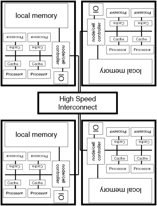
The individual cells or nodes could be fully functioning SMP systems themselves. In fact, a number of implementations have been seen like this, namely IBM's (formerly Sequent) NUMA-Q and Hewlett-Packard's Scalable Computing Architecture (SCA). The high-speed interconnect in those cases is governed by a set of IEEE standards known as Scalable Coherent Interconnect (SCI). SCI is a layered protocol covering everything from electrical signaling, SCI connectors, and SCI cabling all the way to how to keep cache coherency between individual caches in remote nodes. An alternative to SCI is a project undertaken by Stanford University whereby we connect together regular SMP systems, but in doing so we use a device similar to the storage control unit we saw with directory-based cache coherency, to interconnect a group of processors instead of individual processors, which SCI tries to accomplish. This directory controller will perform cache coherency between the nodes/cells whenever a request to a particular memory address or active cache line is made. This architecture is known as DASH (Directory Architecture for SHared memory). In this way, we are attempting to provide a single uniform address space; however, there will need to be fundamental changes to how memory is addressed so an address can be decoded to tell one node/cell which other node/cell a particular memory address is actually located. This should have no impact on individual nodes/cells when operating independently.
The success or failure of a NUMA solution will rest with how non-uniform the access times to remote memory locations are. If the latencies are large, then applications that have processes/threads communicating between each other may see significant performance problems when message-passing via memory slow-downs due to the increased memory latencies. On the other hand, if the latencies are small, the NUMA system will perform like a conventional SMP system without the inherent scalability problems.
Many hardware vendors are starting to employ NUMA architecture in their offerings because the plug-and-play nature of constructing a complex of cells allows customers to configure virtual servers with varying numbers of cells depending on performance and high availability considerations. Hewlett-Packard's cell-based systems like the rp84X0 and Superdome fall into this category, where a cell coherency control maintains the state of cache lines and memory references within and between individual cells. The processors that are used in these servers (PA-8600, PA-8700, PA-8700+) utilize a physical memory address that is encoded with the cell number.
Sun Microsystems offer similar solutions in the SunFire servers, as does IBM with various servers including their high-end p690 UNIX server.
Although hardware architectures support a NUMA-based architecture, the operating system needs to understand these features. HP-UX 11i version 1 had no concept of NUMA features of the underlying architecture and treated available memory as if it were a traditional SMP system. HP-UX 11i version 2 has started to utilize NUMA features by introducing concepts into the operating system such as cell-local memory.
The following NUMA variants are seldom seen as standalone solutions. Commonly, they are implemented as “configuration alternatives” of a cc-NUMA architecture where a particular application/user requirement dictates such a configuration.
NORMA (No Remote Memory Access): Access to memory in other nodes/cells is not allowed.
COMA (Cache-Only Memory Architecture): Here, processors are allowed to access data only in their own cache/memory. If accessing a “remote page,” the “cache controller” will bring the data into memory on the local node, allowing a process on the local node to continue operation. It sounds a lot like cc-NUMA, and in some ways it is. Some would say that early cc-NUMA machines are more like COMA machines. The differences are subtle but distinguishable. I would direct you to the superb book In Search of Clusters, 2nd Edition, by Gregory F. Pfister (ISBN: 0-13-899709-8).
I have left MPP systems out of our discussions because it could fill another entire book. It's not that they are not important; in fact, the Top 500 (http://www.top500.org) supercomputers all employ MPP as their underlying architecture. I will refer you to a quote made by the well-respected computer scientist Andrew S. Tannenbaum (1999): “When you come down to it, an MPP is a collection of more-or-less standard processing nodes connected by a very fast interconnection network.”
Many vendors offer this as a means of gluing together a vast number of individual machines in order to provide massive computational power. Usually, this is at such an expense that only a few organizations can afford or need such machines. Some would argue that an MPP system is loosely coupled because the individual nodes are physically separate. Others would argue that the high-speed interconnect is effectively acting in the same manner as a high-speed interconnect in a NUMA architecture where individual nodes can be viewed as cells, rendering the architecture as tightly coupled.
A cheaper alternative would be to use what is known as a COW (Cluster Of Workstations). Unlike the tightly coupled architecture of MPP, COWs are loosely coupled in that they may utilize their current TCP/IP network as a means of communication. The COW is formed by advanced scheduling software that distributes tasks to individual nodes. Individual nodes could be as simple as a desktop PC. Some people would say that “COWS are supercomputers on the cheap.”
Flynn's Classifications traditionally covers only four architectural definitions. Very few people would argue that this fifth definition truly belongs under the banner of Flynn's Classification. This is more a model for parallel processing. It is almost a hybrid between SIMD and MIMD. This time, the single program is something akin to a standard UNIX program or process. The difference here is that within a process we have multiple independent and differing operations to perform. For example, fluid dynamics involves complex fluid flows where complex equations are required to calculate the behavior at boundaries, e.g., between a pipe and the fluid itself. Our traditional UNIX process can deal with this by spawning a new thread to deal with each boundary condition. The calculations are more complex for boundary than non-boundary conditions. We achieve parallel processing through the use of threads. These programs are run on classical MIMD machines. More system time may be required to manage the additional threads, but overall we hope that the problem will be completed in less real time.
We have spent considerable time looking at the memory hierarchy and issues surrounding processor architectures. Let's discuss other aspects of system design that can influence overall performance.
PA-RISC supports a memory-mapped IO architecture. This simplified architectures allows connected devices to be controlled via LOAD and STORE instructions as if we were accessing locations in memory. There are two forms of IO supported: Direct IO and Direct Memory Access (DMA) IO. Direct IO is the simplest and least costly to the system because it is controlled directly with LOAD and STORE instructions but generates no memory addresses. DMA IO devices, on the other hand, control the transfer of data to or from a range of contiguous memory addresses and is more prevalent than Direct IO devices. PA-RISC organizes its devices by having them connected to one of a number of IO interfaces (known as Device Adapters), which in turn connect to the main memory bus via a bus adapter or bus converter. The main difference between a bus adapter and a bus converter is that a bus adapter is required where we have a non-native PA-RISC bus, while a bus converter is required where we are changing speed from one bus to another. To support a large and varied number of device adapters, PA-RISC supports a large and varied number of bus adapters and bus converters. Overall, IO throughput will be governed by the throughput of all these interfaces. If our main memory bus does not have sufficient bandwidth, then no matter how fast our IO devices are, we won't be able to get the data into memory and, hence, onto the CPU. The morale of the story is this:
Have a good understanding of the IO requirements for each of your systems; if you are using 2Gb Fibre Channel interface cards, will you need the full performance capacity of all those cards all of the time? If so, will your IO bus need to be able to sustain that amount of throughput?
Ensure that your hardware vendor supplies realistic performance figures for all devices involved in the IO path, all the way from the main memory bus to the IO bus involved. This normally means the sustained bandwidth as opposed to the peak bandwidth.
Test, test, and test again.
We don't have the space or time to go through every server in the HP family and discuss the merits of the IO architecture of each of them, so we generalize to an extent and look at one example. Figure A-19 shows a simplified diagram of an HP rp7400.
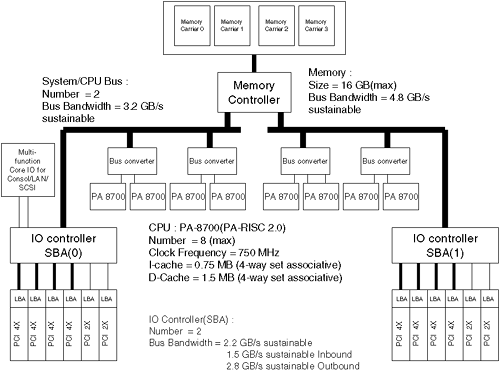
As mentioned previously, there is nothing we can do regarding the bandwidth of the CPU/system and memory bus. In the case of the rp7400, we can choose the CPU and the amount of memory we install. We can also choose which interface cards (Device Adapters) to install. In an rp7400, as is the case with all new HP servers, the underlying IO architecture is PCI. HP currently supports PCI Turbo, PCI Twin-Turbo, and PCI-X.
PCI Turbo (PCI 2X): This interface card is a 5V 33MHz interface card. With a 64-bit data path, a PCI Turbo card is able to supply approximately 250 MB/s transfer rates. These cards can be inserted only in a PCI 2X slot due to the keying on the bottom rail of the card itself.
PCI Twin-Turbo (PCI 4X): This interface card is a 3.5V 66MHz interface card. With a 64-bit data path, a PCI Turbo card is able to supply approximately 533MB/s transfer rates. These cards can be inserted only in a PCI 4X slot due to the “keying” on the bottom rail of the card itself.
PCI-X: These cards either run at 66MHz (PCIX-66) or 133Mhz (PCIX-133), and all cards use 3.5V keying. However, 5V cards are not supported. The throughput for these cards is 533MB/second and 1.06GB/second accordingly.
Universal Card: These cards can be inserted in either a PCI 4X or PCI 2X slot due to the “keying” on the bottom rail of the card supporting both speeds and voltages. The card will adopt the speed of the slot into which it is inserted.
The PCI cards themselves communicate via a Lower Bus Adapter (LBA) ASIC (Application Specific Integrated Circuit), which deals with requests for individual cards. This LBA communicates over an interface known as a rope: PCI-2X and PCIX-66 require one rope and PCI-4X and PCIX-133 need two ropes to communicate with the IO controller known as a System Bus Adapter (SBA).
We would then have to consider the performance of each of the interface cards (device adapters) themselves. For instance, using a 1Gb/s Fibre Channel card is going to perform at a maximum of 128 MB/s. Should we use this in a PCI-2X slot or a PCI-4X slot? In this case, it may make more sense to use a PCI-2X slot leaving the faster slots for higher performing cards. If we look at the design of the SBA IO controller, it can sustain 2.2GB/s overall throughput. We have four PCI-4X cards plus two PSI-2X cards. To really push an rp7400 SBA, we would have to load all slots with cards, which could push the LBA chip to its maximum throughput. The designers have obviously realized that without this capacity the IO subsystem would be a significant bottleneck for this server. As we see more and more high-performance interface cards, we will see a progression to the faster PCI-X interface on HP servers. This will require us to rethink the performance of our IO controllers themselves.
We have mentioned Fibre Channel, and we talk about it again in our discussions regarding solutions for High Availability Clusters. Fibre Channel appears to be the preferred method for attaching disk drives to our servers, although all of the various SCSI standards are supported.
Disk drives and other magnetic storage devices are at the bottom of the memory hierarchy. They are the slowest and least reliable devices in this hierarchy. We look at aspects of High Availability to alleviate disk drives being Single Points Of Failure. Our discussions here deal with the dilemma of storage versus speed. It is a dilemma because hardware vendors continue to produce disk drives with higher and higher capacities, but the underlying performance does not always keep pace. As our users become more and more hungry for storage, it is easy to fall into the trap of using bigger and bigger disk drives. We need to approach the dilemma of storage or speed with a little knowledge of how we interface with disk drives.
Commonly, we will read or hear of performance metrics of the kind “XX MB/s transfer rate.” These performance figures can sound impressive, but they are normally related to a continuous, sequential data stream to and/or from the disk. We need to ask ourselves whether this is a typical workload for one of our disk drives. In some situations, this may be the case. In most commercial applications, we will be performing IO with a smaller unit of transfer and in a more random fashion. The way we try to alleviate these problems is to use some form of data striping, whereby data is spread over multiple spindles and the overall IO workload is spread over multiple disks. In this way, we are trying to minimize the transfer rate by spreading the overall number of IO between multiple devices. Let's also look at another way we could measure disk performance. In the situation we describe above, we were interested in how the disk performed with smaller random IO. In this way, we are really more interested in the way the disk can respond to multiple IO requests. This is usually measured in IO per second (IO/s). Most disk manufacturers don't readily publish these figures, although if you know some basic performance figures for a disk, you can work it yourself. In this example, we are trying to calculate the time to perform an IO. We need three pieces of information:
Access time: This is the time it takes to move the read/write heads into position. This figure is available from disk manufacturers and is usually one of their published performance metrics. For disks in a typical server, this is typically around 5ms (PC disks are usually up to twice as slow).
Latency time: This is the time it takes to spin the disk platters into place. We have to realize that about 50 percent of the time the disk sectors we require will be an entire revolution away. The closest figure published that deals with latency is the number of revolutions per minute (RPM). Again, we will use an average disk for a server. Typical speed = 12000 RPM.
Latency Time = 12000/60(seconds) 200 RPS => 1 revolution will take 5 ms.
Due to the fact that on average, 50 percent of the time, the sectors we require are an entire revolution away, we can say that Latency Time = 2.5ms
Transfer time: This is a very small figure because it is simply the time for the read/write heads to detect the magnetic charge stored on the disk platter. This is typically as small as 0.5ms
time_ to_ perform_ IO = access_ time + latency_ time + transfer_ time
time_ to_ perform _IO = 5ms + 2.5 ms + 0.5 ms
Time to perform IO = 8ms
This eventually gets us to the figure we have been looking for regarding IO/s. If one IO takes 8ms, we can perform 125 IO/s on average. If we know the unit block size that our applications (possibly a filesystem) are using to transfer data to and from the disk, we can get some idea of the expected throughput from our disks.
Always take care when reading performance metrics for disks, especially large disk arrays, because they will often quote you best-case scenarios. If manufacturers don't or won't tell you the IO/s rate, then try to calculate it yourself. This figure represents how quickly a disk can react to IO. This is going to be important when your users are performing lots of small reads and write to their database. For large disk arrays, the IO/s figure quoted is normally when reading from on-board cache. This means that the disk array is not actually reading from disk, so it is not reflecting how the disk array handles requests which require disk access; it's just telling you how well organized its cache is. In real life, it is often the case that our applications will be read from the cache of a disk array, but the data had to get into the cache at some time and that involves reading from disk.
The first source of information is always the documentation for your system. Hardware vendors such as Hewlett-Packard provide copious amounts of information in paper form, on CD-ROM/DVD, or on online. An invaluable and free source of information is the HP documentation Web site: http://docs.hp.com.
Next, we look at some utilities available on your systems themselves. I assume that you are familiar with commands like ioscan, diskinfo, and dmesg. In Chapter 6, “Monitoring System Resources,” we discussed the STM Diagnostic suite of programs. These are exceptionally useful for finding information relating to processor speed, memory bank configuration, and disk drive errors, as well as diagnostic information logged by the diagnostic daemons.
Another way to gather information from your system is to extract values directly from the kernel. This is a problem because you must know the kernel variables that you are looking for in order to extract their values. Here are some examples:
To get the speed of your processor:
root@hpeos003[] echo "itick_per_usec/D" | adb /stand/vmunix /dev/kmem
itick_per_usec:
itick_per_usec: 750
root@hpeos003[]
To establish how much memory is configured (expressed in number of pages; 1 page = 4KB):
root@hpeos003[] echo "phys_mem_pages/D" | adb /stand/vmunix /dev/kmem
phys_mem_pages:
phys_mem_pages: 262144
root@hpeos003[]
This equates to 262,144 pages at 4KB per page, which is 1GB of physical RAM. The amount of free memory that we currently have (again, expressed in pages) is:
root@hpeos003[] echo "freemem/D" | adb /stand/vmunix /dev/kmem
freemem:
freemem:        196867
root@hpeos003[]
The next example explores what happens when we get to a situation where we are trying to diagnose a significant memory shortage. Trying to run any performance-related commands is difficult. There is a kernel parameter that can send diagnostic information to the console. The parameter is vhandinfoticks. If we set this to a value representing a time period, every time period we will get info from the kernel regarding the virtual memory system usage. This information is useful only to a Response Center Engineer if you are having serious virtual memory problems. Below I have set the time period to 10 seconds; 1 tick = 10 milliseconds, 1000 ticks = 10 seconds:
root@hpeos003[] echo "vhandinfoticks/D" | adb /stand/vmunix /dev/kmem
vhandinfoticks:
vhandinfoticks: 0
root@hpeos003[]

root@hpeos003[] echo "vhandinfoticks/D" | adb /stand/vmunix /dev/kmem
vhandinfoticks:
vhandinfoticks: 0
root@hpeos003[] echo "vhandinfoticks/W3E8" | adb -w /stand/vmunix /dev/kmem
vhandinfoticks: 0               =       3E8
root@hpeos003[]
root@hpeos003[] echo "vhandinfoticks/D" | adb /stand/vmunix /dev/kmem
vhandinfoticks:
vhandinfoticks: 1000
root@hpeos003[]
The last of these examples is a kernel variable that I think is quite useful. The kernel variable is called boot_string. The kernel maintains it at boot time, and it shows the ISL command used to boot the system. This kernel variable also shows us the hardware path of the disk we booted from; this is sometimes useful in a mirrored disk configuration:
root@hpeos003[] echo "boot_string/S" | adb /stand/vmunix /dev/kmem
boot_string:
boot_string:    disk(0/0/1/1.15.0.0.0.0.0;0)/stand/vmunix
root@hpeos003[]
I have also included the source code for two C programs, one called infocache32 the other called infocache64 (see Appendix B for the source code for both programs). The reason for two is that there are two separate but similar system calls used in both programs: nlist() and nlist64(). nlist() is for a 32-bit architecture, while nlist64()is for a 64-bit architecture. PA-RISC 2.0 supports 64-bit or 32-bit HP-UX, while PA-RISC 1.X supports only 32-bit HP-UX. To check whether your system is 32-bit or 64-bit capable, run this command:
root@hpeos002[] # getconf HW_CPU_SUPP_BITS
32
root@hpeos002[] #
If we see the value 32, this means that we only support 32-bit HP-UX. A value of 32/64 means that we can support either 32-bit or 64-bit HP-UX, while a value of 64 means that we support only 64-bit PH-UX. There is also a kernel parameter that details which architecture we are running with:
root@hpeos002[] # nm /stand/vmunix | grep cpu_arch
cpu_arch_is_1_0     |   9959824|extern|data   |$SHORTDATA$
cpu_arch_is_1_1     |   9959760|extern|data   |$SHORTDATA$
cpu_arch_is_2_0     |   9959996|extern|data   |$SHORTDATA$
root@hpeos002[] #
root@hpeos002[] # echo "cpu_arch_is_2_0/D" | adb /stand/vmunix /dev/kmem
cpu_arch_is_2_0:
cpu_arch_is_2_0:                0
root@hpeos002[] #
We also need to be sure that we are actually running 32-bit HP-UX because a 64-bit machine could have been running HP-UX version 10.20 and upgraded to 11.X. This would mean that the operating system was still 32-bit. We can check the bit-size of the kernel by using getconf again:
root@hpeos003[] getconf KERNEL_BITS
64
root@hpeos003[]
This has a direct impact on which version of infocache we use and how to compile it:
Use the appropriate program for the bit-size of your operating system.
Use the appropriate option (+DD32 or +DD64) to compile the program.
I have seen many incarnations of this program over time. Recently, I saw a version on Hewlett-Packard's IT Resource Center (http://itrc.hp.com). Below, you can see the output from building and running infocache on an HP 715 running HP-UX 11i as well as an A500 server.
root@hpeos002[] # getconf KERNEL_BITS
32
root@hpeos002[] # model
9000/715/G
root@hpeos002[] # ll infocache32.c
-rw-r-----   1 root       sys           2336 Aug 10 18:46 infocache32.c
root@hpeos002[] # cc +DD32 -lelf -o infocache32 infocache32.c
root@hpeos002[] # ./infocache32
Kernel = /stand/vmunix

HW page size is 4096 bytes
HW TLB walker present
TLB is unified
TLB size is 64 entries

Cache is separate
I cache size is 131072 bytes (room for 32 pages)
D cache size is 131072 bytes (room for 32 pages)

One cache line is 32 bytes
Cache lines per chunk: 1
root@hpeos002[] #
This is the same program, but it was compiled and run on a 64-bit machine (an A500 server):
root@hpeos003[] model
9000/800/A500-7X
root@hpeos003[]
root@hpeos003[] getconf KERNEL_BITS
64
root@hpeos003[]
root@hpeos003[] echo "cpu_arch_is_2_0/D" | adb /stand/vmunix /dev/kmem
cpu_arch_is_2_0:
cpu_arch_is_2_0:                1
root@hpeos003[] ll infocache64.c
-rw-r-----   1 root       sys           2344 Nov 22 12:48 infocache64.c
root@hpeos003[] cc +DD64 -lelf -o infocache64 infocache64.c
root@hpeos003[] ./infocache64
Kernel = /stand/vmunix

HW page size is 4096 bytes
NO HW TLB walker
TLB is unified
TLB size is 240 entries

Cache is separate
I cache size is 786432 bytes (room for 192 pages)
D cache size is 1572864 bytes (room for 384 pages)

One cache line is 64 bytes
Cache lines per chunk: 1
root@hpeos003[]
We have discussed many aspects of system architecture to familiarize ourselves with a number of concepts prevalent in today's high-performance systems. We started with a discussion of processor architecture including a discussion of Hewlett-Packard's two main processor architectures: PA-RISC and IA-64. We moved on through the memory hierarchy and then disk drives. We concluded our discussions with a look at ways to familiarize yourself with the hardware on your HP-UX server(s). Don't forget about the standard commands available on HP-UX to perform this task, commands such as ioscan, dmesg, lanscan, and fcmsutil to name a few. The alternative approaches we looked at were simply that: alternatives. Once we know what hardware we are dealing with, we can move to the many different aspects of managing this hardware. Read the questions at the end of this section to see whether you understand the material covered.
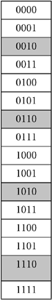
[1] There is much intellectual pie throwing between the EDVAC and ENIAC camps. John W. Mauchly and J. Presper Eckert, Jr., engineered ENIAC (Electronic Numerical Integrator and Calculator) around the same time as EDVAC. There is a long-running debate among academics as to which machine really came first. To this day, the architecture is still known after John von Neumann.