
How does this difference manifest in terms of the actual design of the processor itself? This diagram, taken from NVIDIA's own CUDA documentation, illustrates these differences:
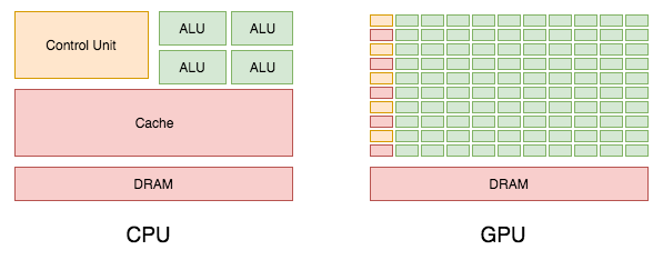
Control or cache units are reduced, while there is a significant increase in the number of cores or ALUs. This results in improvement of an order of magnitude (or more) in performance. The caveat to this is that GPU efficiency is far from perfect with respect to memory, compute, and power. This is why a number of companies are racing to design a processor for DNN workloads from the ground up, to optimize the ratio of cache units/ALUs, and to improve the way in which data is pulled into memory and then fed into the compute units. Currently, memory is a bottleneck in GPUs, as illustrated by the following diagram:

The ALUs can only work if they have something to work on. If we exhaust the on-die memory, we have to go to the L2 cache, which is faster in a GPU than in a CPU, but still takes far longer than on-die L1 memory to access. We will discuss these shortcomings in the context of new and competing chip designs in a later chapter. For now, the important thing to understand is that, ideally, we want to have as many ALUs and as much on-die cache as we can cram into a chip, in the right ratio, and with fast communication between the processors and their memory. For this process, CPUs do work, but GPUs are far better. And for now, they are the most suitable hardware for machine learning that is widely available to consumers.