
Intel's response to Texas Instrument's successful TMS 1000 MCU was the MCS-48 series, with the 8048, 8035, and 8748 being the first models released in 1976. The 8048 has 1 KB of ROM and 64 bytes of RAM. It is an 8-bit design with a Harvard architecture (split code/data memory), introducing a native word size of 8 bits and interrupt support (two single-level) and is compatible with 8080/8085 peripherals, making it a highly versatile MCU. The advantage of wider ALU and register word sizes is still perceivable today, where for example a 32 bit addition is sequentially executed on an 8 bit MCU as a series of 8 bit additions with carry.
The MCS-48 features over 96 instructions, most of them a single byte in length, and allows for external memory to be added in addition to the internal memory. In a community effort, available information on the MCS-48 family has been compiled and released at https://devsaurus.github.io/mcs-48/mcs-48.pdf .
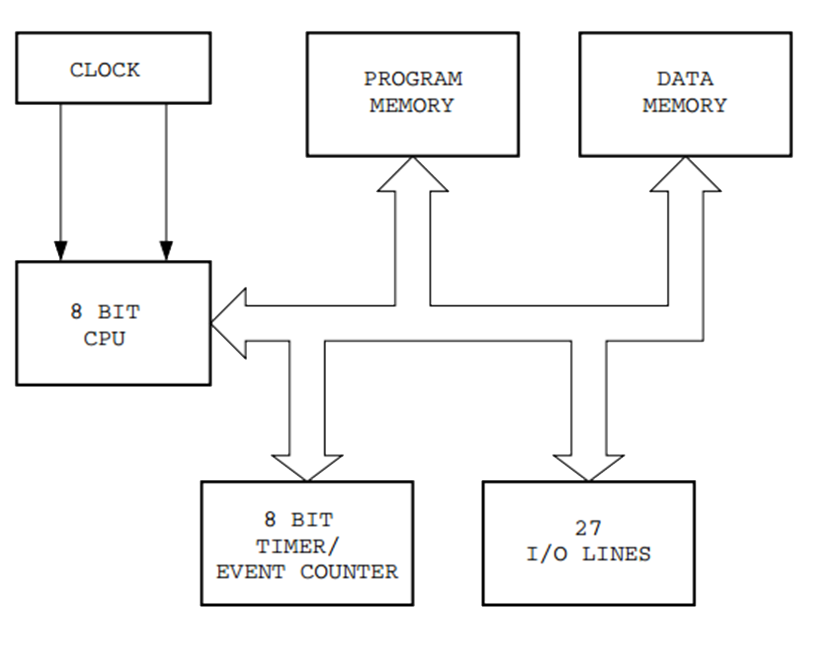
Here we consider the simplicity of the MCS-48 functional block diagram and compare it to that of its successors as follows:
Even for a design that was introduced just a few years after the TMS 1000, the rapid evolution of MCU designs is evident. Since MCU design evolved alongside popular CPU designs of the time, including the 6502, its 16-bit version, and what would eventually become the M68K processor family, there are many similarities to be found.
Due to its flexible design, it remained popular and in production until the 1990s, until the MCS-51 (8051) series gradually replaced it. See the next section for more details on the 8051.
The MCS-48 was used in the keyboard of the original IBM PC as its controller. It was also used with the 80286 and 80386 to perform A20 line gating and reset functions in the case of the former. Later PCs would integrate these features into Super I/O devices.
Other notable uses of the MCS-48 include the Magnavox Odyssey video game console and a range of Korg and Roland analog synthesizers. While masked ROM (up to 2 KB) was an option with the MCS-48 family, the 87P50 used an external ROM module for its programming, and the 8748 and 8749 featured up to 2 KB EPROM, which allowed for the MCU's internal programming to be altered repeatedly.
Like with standalone EPROM modules, this requires the package to contain a fused quartz window, which allows for ultraviolet light to reach the MCU die, as can clearly be seen in the following photograph of an 8749 MCU with EPROM (by Konstantin Lanzet, CC BY-SA 3.0):
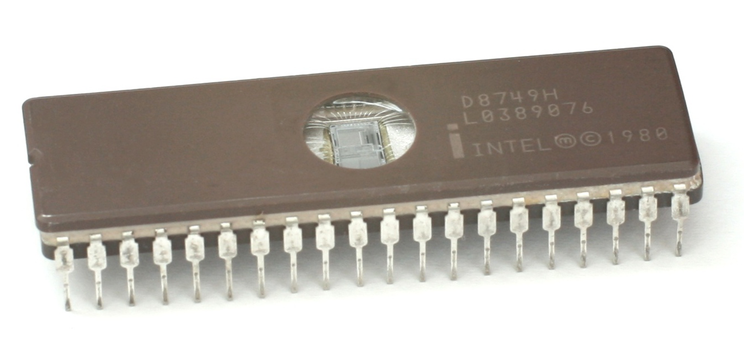
The charge stored in the EPROM cells that defines bits as written dissipates within a 20-30 minute exposure to strong ultraviolet light. The same can be achieved in direct sunlight over the course of a few weeks. The erase cycle usually implies removing the package and putting it in the light tight erasing device. After this, the EPROM can be programmed anew. The specified data retention of an EPROM is about 10-20 years at 85°C, and because the degradation accelerates exponentially with temperature, statements of 100 years or more at room temperature are not uncommon (27C512A: 200 years).
Due to the expense of creating the quartz window and integrating it into the package, one-time programmable EPROMs were used for a while, which allow for the easy programming of an EPROM, but mounted the programmed die in an opaque package so that it could not be reprogrammed any more. Ultimately, EEPROMs became available in the early 1980s, which replaced EPROMs almost completely. EEPROMs can be rewritten about a million times before they begin to develop issues when retaining stored data. Their data retention performance is similar to that of EPROMs.