
5.6. Micro Embossing Processes
The term hot embossing or embossing can be used for a large scale of different structuring processes based on an embossing step. The following section will give a short overview of the manifold of these processes. Nevertheless, a clear definition of the terminology cannot be found in literature.
5.6.1. Roller Embossing
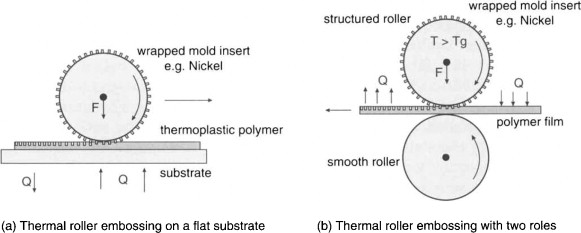
Roller embossing, or roll-to-roll embossing, is a well-established modification of the hot embossing process. Using rolls instead of plates, continuous molding can be achieved with advantages regarding the molding times and disadvantages regarding the height and the aspect ratio of the molded structures (Fig. 5.24). Tan et al. [29] used this approach in 1998–called roller nanoimprint lithography–to fabricate sub-100-nm patterns. Two methods were investigated. The cylinder mold method refers to a thin structured metal film bended around a smooth roller. In particular, a compact disc master with a thickness of 100 μm was used. The second method–here called the flat mold method–refers to a structured silicon wafer mold placed on a polymer substrate. A smooth roller mold is rotated over the mold and the deformation of the mold under the pressure of the roll imprints the structures into the polymer. In both methods the roller temperature is set significantly above the glass-transition temperature. For PMMA the roller temperature was set in a range between 170°C and 200°C and the platform temperature in a range of 50–70°C. Roller speeds from 0.5 cm/sec up to 1.5 cm/sec were investigated, and the pressure was set in a range between 300 psi and 4800 psi.
Figure 5.24. Thermal roller hot embossing. This technology allows a continuous molding. Because of the rotation, the height of the molded structures is limited.
Ng and Wang [25] reported on the hot roller embossing of microfluidic structures with feature sizes down to 50 μm and a corresponding depth up to 30 μm. To fabricate these structures a polymer film was passed between two rollers. The top roller was made of steel wrapped with a structured nickel film with a thickness of 50 μm. The bottom roller, made of rubber, was only a supporting roller. The heat was supplied through the mold and the rollers were applied with force by a clamping unit. The structures were replicated into a PMMA film 1.5 mm thick. The optimal roller temperature was found at 140°C. Embossed depths of more than 30 μm with 100 μm features were achieved at a roller speed of 1.5 mm/sec.
Roller embossing is not limited to thermal structuring; this technique is also suitable for the structuring of UV-curable materials (Fig. 5.25). Chang et al. [6] used this method for the fabrication of microlens arrays on glass substrates. In a first step a nickel mold with microlens structures is fabricated by electroforming and wrapped in a second step onto a cylinder. During rolling the roller presses and drags the UV-curable polymer on a glass substrate through the rolling zone. At the same time the molded structures are cured by UV radiation and guided into the molding zone. With this technology arrays of polymer microlenses with a diameter of 100 μm, a pitch of 200 μm, and a depth of 21 μm on an array of 100 × 100 were fabricated. A suitable roller speed was found in the range between 0.5 mm/sec and 2 mm/sec. The nickel mold wrapped onto the roll was manufactured by several process steps. First, a silicon wafer was structured by photolithography and deep-reactive ion etching. A polymeric master from the silicon wafer was made by gas-pressurized thermoforming of a polycarbonate film. Depending on the pressure size, the holes of the etched silicon wafer were partially filled, resulting in a convex shape of the polymer film. The formed polymer film was silver-coated and finally copied into a nickel mold insert by electroplating.
Figure 5.25. UV-roller hot embossing. The technology of roller embossing is also suitable for UV-curing materials. To cure the molded material, the UV radiation has to be applied at the structuring zone.

Yang et al. [34] fabricated arrays of microlenses by so-called soft roller embossing of a UV-curable resist under the assistance of a gas-pressurized platform. Therefore, a PDMS mold was wrapped onto a cylinder. The fabrication of the mold was similar to the method of Chang described above, with the difference that from the structured polycarbonate film a PDMS casting instead of nickel electroplating was performed. The embossing system was composed of a UV-radiation source, a transparent substrate, the structured roller stamper, a split-coating module, pneumatic cylinders, and a flexible platform with gas-pressurized pad. The soft pad can be deformed by gas pressure and guarantee a conformal contact of a PET substrate between pad and roller. The roller stamping process can be described in three main steps. First, the UV-curable liquid resin is coated onto the soft roller with the microlens array. In a second step, the roller with the resin is brought into contact with the PET film by applying a specific pressure. Finally, the liquid resin is transferred onto the PET film and is cured by UV radiation during rolling. Liu and Chang [17] used the soft roller embossing method without gas-pressurized assistance to fabricate arrays of micro blocks onto a glass substrate. By this design with the structure dimensions of 100 μm × 80 μm and a depth of 40 μm, the process parameters dependent on the structure quality were determined. The maximal depth of 40 μm was achieved only by a decrease in roller velocity down to 0.25 mm/sec.
Theoretical aspects of the roller imprinting process in the case of printing microfluidic devices were investigated by Vijayaraghavan et al. [33]. Especially the effects of process variables like feature spacing, roll radius, roll velocities, molding materials, and design features on the imprint using finite element simulations were analyzed. They found that the feature spacing has the largest impact on the quality of the imprints. The so-called imprint gap–the difference in height between the top of the imprint walls and the undeformed substrate–decreases with increasing feature spacing. For features spaced wider than their width, the imprint gap is negligible. Further, the feature shape does not significantly affect the deformation behavior. The roll radius had a significant impact on the work-piece reaction forces. It was found that larger roll radii result in larger reaction forces, corresponding to the contact area between roll and substrate. Stamping can here be interpreted as an infinite roll radius.
The fabrication of the microstructured roller refers in the cited articles to a fabrication process on flat substrates and additional wrapping around a roller. Jiang et al. [14] presented a method to fabricate a metallic roller mold with microstructures on its surface using a dry film resist. This resist is laminated uniformly onto the surface of an imprinting roller. Using a flexible film photo mask wrapped around the roller, the photo resist can be structured by nonplanar lithography, achievable by rotating of the roller during a UV-lithography step. Finally, the structures in the resist can be transferred into the metallic surface by wet etching. The advantage of this fabrication method is to avoid any sliding problems of wrapped molds during the molding cycle. Further, the metallic surface has a high strength durability and temperature endurance.
Finally, the roller embossing process is not limited to the structuring of polymers. Shan et al. [27,28] demonstrated the structuring of multilayered green ceramic substrates by micro roller embossing using a modified laminating machine. Micro patterns, including channels and electrical passives with a 50 μm line width, were formed over the whole panel area of 150 mm × 150 mm.
5.6.2. Ultrasonic Embossing
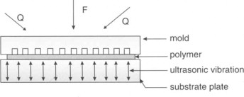
Hot embossing is typically characterized by a conductive or convective heat transfer that requires a comparatively long cycle time for the heating of a polymer film over the glass-transition temperature. Lin and Chen [15] showed a hot embossing concept referring to the principle of ultrasonic embossing. An ultrasonic source is located on the top of the mold insert to generate high-frequency vibrations, causing an increase in temperature of a polymer foil up to the melting range. The ultrasonic vibration rapidly increases the temperature at the contact area between mold insert and polymer film, which means that heating times can be reduced significantly. Because of this principle the temperature distribution between the thermal hot embossing principle and the ultrasonic principle is different. In conventional thermal heating concepts for hot embossing, the temperature distribution inside the polymer melt is nearly identical, whereas in ultrasonic embossing the localized heat-effective zones are concentrated on the contact areas of the mold insert and polymer. Therefore, this ultrasonic embossing method is not an isothermal process. The temperature distribution and the polymer flow dependent on the mold geometry and resist thickness during ultrasonic embossing were simulated by Lint and Chen [16]. The lateral and vertical velocity profiles are described through the contribution of Poiseulle flow and Cuette flow. It was found that, because of the higher temperature at the cavity sidewalls, the polymer flow tends to flow along the cavity sidewalls of the mold. Also, the filling mode (single mode and dual mode, Section 6.4.2) of cavities with different diameters was simulated. In ultrasonic vibration both modes are visible. Cavities with wider convexity and thinner resists form a dual-peak mode; in contrast, therefore, a wider cavity and a thicker mold insert form a single peak.
Mekaru et al. [20] implemented an atmospheric hot embossing process on almost the same conditions as vacuum hot embossing combined with ultrasonic vibration (Fig. 5.26). The synergy effect of the conventional load (press force) and ultrasonic vibration can optimize the flow behavior to fill microcavities. In this work, longitudinal waves were generated by an ultrasonic system with a 15 kHz and 900 W output. With this technique, micro pyramids in the size of 100–530 μm and depth up to 260 μm were replicated in polycarbonate. The molding step consists of a conventional heating step of the polymer over the glass-transition temperature and a following molding step in which the mold is pressed into the polymer melt. During the pressing and the following holding time, the ultrasonic vibration is active. After the holding time, the ultrasonic vibration is stopped and the cooling cycle starts up to a temperature below glass-transition temperature. The demolding can be done with the support of ultrasonic vibration. The result of these experiments shows that contact force and contact times are decreased by applying ultrasonic vibration. With this method it is further possible to mold under atmospheric conditions.
Figure 5.26. Principle of ultrasonic embossing in combination with a conventional thermal embossing process. The substrate plate is exposed by ultrasonic vibration.
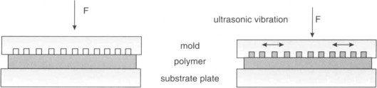
Another approach for ultrasonic molding was presented by Cross et al. [10]. This approach refers to a room-temperature forming of solid films, which are not structured by thermal support (Fig. 5.27). The principle of small amplitude (<10 nm) oscillatory shear forming (SAOSF) is based on two steps. First, a structured mold or a stamper is pressed with a normal contact load (in this case, 50 MPa) into a thin solid film, for example, polystyrene. In a second step, plastic strains are generated by augmenting the normal contact load with a small oscillatory motion in the plane of the film. Finally, after sufficient cycles, mold and film are separated.
Figure 5.27. Principle of ultrasonic embossing at room temperature. Because of the ultrasonic vibration, the polymer is heated up at the contact area to molding temperature. The vibration can be effected horizontally in the plane of the film or, alternatively, in a vertical direction.
5.6.3. Gas-Assisted Embossing
The act of force during the embossing step is mainly characterized by direct contact of rigid plates or roles. The force is typically effected by hydraulic drive units or spindle drives. The contact of rigid plates, for example, requires typically smooth and even surfaces to guarantee a homogeneous contact over the whole molding area, especially if the molding area increases. Further, brittle silicon molds, for example, can be difficult to use in combination with a rigid substrate plate because of the stress concentration during molding caused by uneven substrate plates. The use of gas as an acting load during molding can prevent especially brittle materials from damaging. Pressurized gas is similar to the process of thermoforming. Here the temperature determines the kind of molding process. If the temperature is in the range of the glass-transition temperature of the polymer, the molding is mainly characterized by strain deformation and the molding process is defined as a thermoforming process (see Section 2.6). If the molding temperature increases significantly into the melting state of the polymer, then the forming is mainly characterized by shear, which is a criterion for molding processes. Therefore, the molding or forming temperature is an indication for the classification of the gas-assisted molding process.
Independent from the investigations of micro thermoforming by Truckenmüller [31] in 2003, Chang and Yhang [8] presented a concept for gas-assisted hot embossing with four main molding steps. First, inside a closed chamber with gas inlets and outlets a polymer film is placed onto a microstructured stamper. In a second step, the chamber is closed and the stack of stamper and polymer foil is heated up to molding temperature. After the molding temperature is achieved, the chamber is flooded with nitrogen gas at high pressure. The gas pressure acts uniformly over the whole microstructured stamper and forms the polymer film into the cavity. After cooling, the gas pressure is exhausted and the molded part can be demolded by peeling. By this technique, also double-sided molding was demonstrated using a stack of two molds with a polymer film in between. The gas pressure acts in this case onto a polymer seal film covering the stack (Fig. 5.28). By this technique a 200 μm thick PVC film was structured at 90°C, and a double-sided molding was tested by a 2 mm thick PMMA sheet heated up to a molding temperature of 155°C. The pressure of 40 kg/cm2 refers to a 4-inch silicon mold with microfluidic channels. Yang et al. [34] used this technology to replicate V-grooves by CO2-assisted embossing into PMMA at temperatures between 25°C and 130°C on an area of 90 mm × 90 mm. The grooves were characterized by a width of 50°C and a depth of 21 μm. The nickel mold was applied by pressures of 10 bar. Chang et al. [7] fabricated microlens arrays by using gas pressure to form polycarbonate films into etched holes of a silicon mold. An array of 300 × 300 microlenses with a diameter of 150 μm and a pitch of 200 μm were replicated. For polycarbonate, a forming temperature of 150°C and a pressure load of 10–40 kg/cm2 during 30 seconds up to 90 seconds were implemented. In this example, the temperature range is close to the glass-transition range of polycarbonate, which characterizes the forming mainly by strain deformation. Therefore, this is also an example for the micro thermoforming process (Fig. 5.29).
Figure 5.28. Principle of gas-assisted double-sided hot embossing. A seal separates the aligned mold inserts with the polymer between and the gas volume. After heating the polymer over its glass-transition temperature, the gas pressure acts as a press force similar to the conventional hot embossing steps.
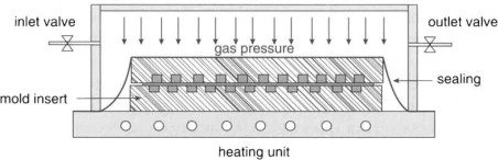
Figure 5.29. Principle of gas-assisted thermoforming of microlenses [7]. A polymer film is placed onto a microstructured stamper with holes, is heated up to forming temperature, and is formed by air pressure into the cavities. The embossing temperature is close to the glass-transition temperature, where the forming is characterized by strain. In this case, the molding principle is defined as thermoforming (Section 2.6) [32].

The molding by gas pressure can be miniaturized to single molding elements integrated in a silicon mold (Fig. 5.30). This concept was investigated for thermal nanoimprinting by Pedersen et al. [26]. The concept refers to single air cavities at the back side of a stamp allowing gas pressure to act at the structured areas of a mold. To obtain a minimal bending of the brittle silicon, the back side of the structured areas has be etched to a remaining thickness of around 150 μm. Silicon with this thickness allows a bending under air pressure that is sufficient for the molding of nanostructures. In this case, the depth of the molded structures was in a range below 200 nm. The concept was implemented by bonding a lid containing access holes to the back side of the flexible stamp forming a so-called intrastamp cavity. If after heating of the components gas is pumped into the cavities at the back side, the pressure acts as load for imprinting. Due to the flexibility of the thin remaining layer of the stamper, only moderate pressure is required. If after cooling the back-side cavities are evacuated, the direction of the structured remaining layer changes and the molded structures can be demolded. This concept was implemented for a silicon stamper with more than 1,500 imprint areas of 1 mm × 1 mm separated 0.5 mm from each other. Imprints were performed in PMMA films with a thickness of 305 nm. With this technique, homogeneous imprints across an area of 35 mm diameter were achieved.
Figure 5.30. Principle of smart stamps for gas-assisted embossing. Small cavities at the back side of a silicon wafer are etched at selected areas to a residual thickness of 150 μm. An bonded back lid forms a so-called intrastamp with an area of around 1 mm × 1 mm. Gas pressure acting on the back side of the stamper can deform the thin residual layer of the silicon wafer. After heating, these stamps can be used for thermal imprinting and also, after cooling, for demolding.

5.6.4. UV Embossing
UV embossing is a method similar to the UV nanoimprint process (Section 2.7.2). A UV-curable resin is coated on a substrate, imprinted by a structured mold insert and cured by UV radiation. Molding with UV-curable materials does not require heating systems and, because of the typically low viscosity of the UV-curable materials, only moderate embossing pressures are needed, which results in smaller UV-imprint machines. Chan-Park and Neo [5] used this method for the fabrication of micro cups. A UV-curable resin was embossed at room temperature onto a nickel mold by a rubber-coated laminating roller and in a second step cured by UV radiation. The demolding of the embossed micro cups was achieved by peeling.
5.6.5. Soft Embossing
The process of soft embossing refers to a mold fabricated of elastic materials. A common material is polydimethylsiloxane (PDMS). This elastomeric material can be used because of its thermal stability up to 200°C and its transparency for UV radiation as a mold insert for thermal nanoimprinting, UV nanoimprinting, and hot embossing. Typically, the mold inserts are fabricated by casting from a master, fabricated by lithographic or etching processes. Because of the flexibility of this material, demolding by peeling from a master can be performed without any deformations of structures. Further, PDMS is chemically inert and is characterized by a low surface energy [18]. The properties of PDMS are therefore advantageous for demolding of embossed structures. During molding, an elastic material guarantees a conformal contact between the mold and the polymer independent of unevenness of any substrate plates. Nevertheless, compared to a rigid mold material an elastic mold tends to deform under load, which can result in a loss of precision in lateral dimensions of molded structures, especially if high molding forces are required.
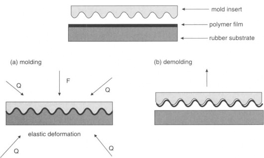
Carvalho et al. [4] replicated microfluidic devices with a feature size of 127 μm and a depth of 50 μm by soft embossing with a silicone mold casted from a micro-milled master. Rubber-assisted hot embossing was performed by Nagarajan and Yao [24]. In this work thin polystyrene film with a thickness of 25 μm was patterned with micro grooves in the dimension of 100 μm. In contrast to an elastic mold insert, an elastic rubber was used as the substrate plate (Fig. 5.31). The microstructured rigid mold insert was fabricated by electrical discharge machining. The polymer film is placed between the hard die and the rubber substrate. The metal die is heated up over the softening range of the polymer and pressed into the cold rubber substrate. The rubber substrate deforms under load and acquires the profile of the die, acting as negative counter tool to the positive metal die. By this method a conformal contact between hard mold insert and substrate is achievable, forming the enclosed thin polymer film. The following process steps of force-controlled molding and cooling under load are similar to the process steps of hot embossing. Finally, the ejection of the formed part can be performed by the help of the elastic rubber substrate forming back to the initial shape and ejecting the formed part. The elastic rubber substrate can be used many times. Regarding the temperature range and the forming method, rubber embossing is closely related to the process of micro thermoforming.
Figure 5.31. Thermoforming of a polymer film on an elastic rubber substrate. A polymer film is placed between a hard mold insert and a rubber substrate. The metal mold insert is heated up over the softening range of the polymer and pressed into the cold rubber substrate. The rubber substrate deforms under load and acquires the profile of the mold insert. The deformation of the rubber substrate is reversible.
Huang et al. [13] used the soft embossing technology for the fabrication of micro-ring optical resonators. First, a master was fabricated by E-beam lithography. From this master the mold was copied by casting of PDMS. This mold was finally used for a UV-embossing process to mold a UV-curable resist, which is cured by UV radiation and peeled off from the elastic mold. The ring diameter of the replicated structures was 200 μm, the waveguide width was 2 μm, and the gap between the straight waveguide and the micro ring was 250 nm. The measurement of the optical properties compared to a master device shows that the optical properties of the molded parts are nearly identical, which makes this technology well suited for the replication of optical waveguides and resonator structures.
5.6.6. 3D Embossing
The replication by hot embossing mostly refers to so-called 2.5-dimensional structures, structures with the same level of height and vertical sidewalls or structures with demolding angles. Nevertheless, the molding of real three-dimensional (3D) structures is also possible if the structures are characterized by the lack of undercuts that prevent a successful demolding with a conventional technique. Tormen et al. [30] investigated the fabrication of 3D structures by an approach on a combination of lithographic steps and isotropic wet etching. The optical structures were performed on quartz or glass substrates with very accurate shape and nanometer scale surface roughness. The structures were finally replicated in cyclic polyolefin (COC) by hot embossing.
Regarding the combination of rigid mold and thermoplastic polymers, it is obvious that 3D structures with undercuts like dovetails cannot be demolded without damaging the mold insert or the molded structures. A simulation of the demolding cycle (Section 6.4.4) shows that, for structures with a height of 100 μm and a deviation of 0.25 μm from the vertical, the demolding force doubles.
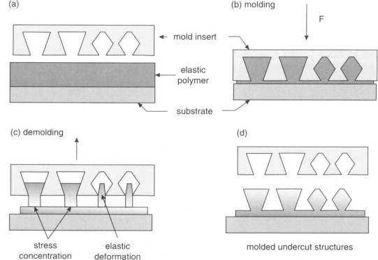
To avoid damaging structures with undercuts, one of the components–the mold insert or the molded part–should have elastic properties so that the demolding can be performed under reversible elastic deformation (Figs. 5.32 and 5.33). In this case the elastic material PDMS has the potential for the replication of 3D structures. Bogdanski et al. [3] investigated the molding of undercut structures over an area of 5 × 5 cm2 by structuring PDMS with an etched silicon mold. The undercuts of the structures were in a range between 0.5 μm and 10 μm compared to a vertical trench of the structures of 1 μm up to 15 μm. The replication of these structures in PDMS showed a loss in the sharpness of the edges and a tear off of the structures during demolding if the thickness of the residual layer was in a range of the undercut width. For a thicker residual layer, the connection between structures and residual layer was strong enough to withstand the tensile forces during demolding. Independent of this work, it is also possible to mold and demold structures if a PDMS mold insert is used and the undercut structures are molded in thermoplastic polymers. Finally, the design of undercuts determines the demolding forces and defines the potential of successful replication.
Figure 5.32. Principle of soft embossing of 3D structures using an elastic mold insert. Because of the elasticity of the mold material 3D structures can be demolded. During demolding, the structures of the mold insert are elastically deformed and prevent the molded polymer from deformation.

Figure 5.33. Principle of soft embossing of 3D structures using an elastic polymer. Because of the elasticity of the molding material 3D structures can be demolded. Depending on the design and the cross-section, the structures can be torn off during demolding.
5.6.7. Hot Embossing of Conducting Paths–MID Hot Embossing
The integration of conduction paths into microsystems is fundamental for the connection of mechanical or fluidic devices to electrical control units or signal analyzers or for the appropriation of a potential difference, for example, in capillary electrophoresis systems (Section 10.3.1).
An example for the integration of conducting paths into molded microstructures by hot embossing was investigated by Heckele and Anna [12]. In a first step, preliminary conducting paths in terms of a gold layer of a few 100 nm in thickness were sputtered through a mask onto a polymer film. In a second step, these thin paths were increased by electroplating of gold up to a thickness between 0.3 μm and 3 μm. In a following step, the polymer film with the paths on top was embossed with a microstructured mold with a structure height of 130 μm. The LIGA mold was characterized by vertical sidewalls and additionally by structures with 45 degree angles. The molding results show that the conduction paths maintain their lateral shape and are not deformed by polymer molding. Further, because of the ductility of gold, the paths do not break when passing steps, independent of the angle of the step (45° edges and also 90° edges). In the case of vertical steps, the conducting paths do not follow the sharp edges; the paths are instead submerged into the polymer.
Hot embossing of conduction paths is also an established process for the fabrication of molded interconnected devices (MID) [1]. By this hot embossing technology electronic circuits are embossed on top of already molded polymer components (Fig. 5.34). First, the layout of an electronic circuit is copied into a metal mold insert by mechanical structuring methods, for example, milling. A copper foil is placed between the mold insert and the surface of the molded part. The mold insert is heated up to a molding temperature of 20–40°C over the glass-transition temperature (amorphous polymer) or melting temperature (semicrystalline polymer) of the molded part. If the molding temperature is achieved, the mold insert and the copper foil are pressed by the protruding structures of the mold insert onto the surface of the molded part. The conductor lines are punched out and are connected with the thermoplastic substrate. The connection refers to adhesion because of the roughness of the back side of the copper foil in the range of typically Ra 0.5–2 μm. During the embossing state the polymer melt is displaced, resulting in a bulge beside the conducting paths. The height of this bulge is a function of the polymer material, the temperature of the mold, the embossing time, and the depth of impression.
Figure 5.34. Embossing of conduction paths on molded interconnected devices (MID). A copper foil is placed between mold insert and molded part. If after heating the molding temperature is achieved, the mold insert and the copper foil is pressed by structures of the mold insert onto the surface of the molded part. The conductor lines are punched out and are connected with the thermoplastic substrate by adhesion.
