
17
Multilevel Power Converters
King Mongkut's Institute of Technology Ladkrabang, Thailand
The University of Tennessee, Department of Electrical Engineering and Computer Science, Knoxville, Tennessee, USA
17.1 Introduction
17.2 Multilevel Power Converter Structures
17.2.1 Cascaded H-Bridges
17.2.2 Diode-Clamped Multilevel Inverter
17.3 Multilevel Converter PWM Modulation Strategies
17.3.1 Multilevel Carrier-Based PWM
17.3.2 Multilevel Space Vector PWM
17.4 Multilevel Converter Design Example
17.4.1 Interface with Electrical System
17.4.2 Number of Levels and Voltage Rating of Active Devices
17.4.3 Number and Voltage Rating of Clamping Diodes
17.4.4 Current Rating of Active Devices
17.5 Fault Diagnosis in Multilevel Converters
17.6 Renewable Energy Interface
17.7 Conclusion
17.1 Introduction
Numerous industrial applications require higher power apparatus in recent years. Some medium-voltage motor drives and utility applications require medium voltage and megawatt power level. For a medium-voltage grid, it is troublesome to connect only one power semiconductor switch directly. Hence, a multilevel power converter structure has been introduced as an alternative in high power and medium voltage situations. A multilevel converter not only achieves high power ratings but also enables the use of renewable energy sources. Renewable energy sources such as photovoltaic, wind, and fuel cells can be easily interfaced to a multilevel converter system for a high-power application [1–3].
The concept of multilevel converters has been introduced since 1975 [4]. The term multilevel began with the three-level converter [5]. Subsequently, several multilevel converter topologies have been developed [6–13]. However, the basic concept of a multilevel converter to achieve higher power is to use a series of power semiconductor switches with several lower voltage dc sources to perform the power conversion by synthesizing a staircase voltage waveform. Capacitors, batteries, and renewable energy voltage sources can be used as the multiple dc voltage sources. The commutation of the power switches aggregate these multiple dc sources to achieve high voltage at the output; however, the rated voltage of the power semiconductor switches depends only on the rating of the dc voltage sources to which they are connected.
A multilevel converter has several advantages over a conventional two-level converter that uses high switching frequency pulse width modulation (PWM). The attractive features of a multilevel converter are summarized as follows.
• Staircase waveform quality: Multilevel converters not only can generate the output voltages with very low distortion but also can reduce the dv/dt stresses; therefore, electromagnetic compatibility (EMC) problems can be reduced.
• Common-mode (CM) voltage: Multilevel converters produce smaller CM voltage; therefore, the stress in the bearings of a motor connected to a multilevel motor drive can be reduced. Furthermore, CM voltage can be eliminated by using advanced modulation strategies such as that proposed in [14].
• Input current: Multilevel converters can draw input current with low distortion.
• Switching frequency: Multilevel converters can operate at both fundamental switching frequency and high switching frequency PWM. It should be noted that lower switching frequency usually means lower switching loss and higher efficiency.
Unfortunately, multilevel converters do have some disadvantages. One particular disadvantage is the requirement of greater number of power semiconductor switches. Although lower voltage rated switches can be utilized in a multilevel converter, each switch requires a related gate drive circuit. This may cause the overall system to be more expensive and complex.
Many multilevel converter topologies have been proposed during the last two decades. Contemporary research has engaged novel converter topologies and unique modulation schemes. Moreover, three different major multilevel converter structures have been reported in the literature: cascaded H-bridges converter with separate dc sources, diode clamped (neutral clamped), and flying capacitors (capacitor clamped). Moreover, abundant modulation techniques and control paradigms have been developed for multilevel converters, such as sinusoidal pulse width modulation (SPWM), selective harmonic elimination (SHE-PWM), space vector modulation (SVM), and so on. In addition, many multilevel converter applications focus on industrial medium-voltage motor drives [11,15], utility interface for renewable energy systems [16], flexible ac transmission system (FACTS) [17], and traction drive systems [18].
This chapter reviews the state of the art of multilevel power-converter technology. Fundamental multilevel converter structures and modulation paradigms are discussed including the pros and cons of each technique. The main focus is on modern and more practical industrial applications of multilevel converters. A procedure for calculating the required ratings for the active switches, clamping diodes, and dc link capacitors including a design example is described. Finally, the possible future developments of multilevel converter technology are noted.
17.2 Multilevel Power Converter Structures
As mentioned earlier, three different major multilevel converter structures have been used in industrial applications: cascaded H-bridge converter with separate dc sources, diode clamped, and flying capacitors. It should be noted that the term multilevel converter is utilized to refer to a power electronic circuit that could operate in an inverter or rectifier mode. The multilevel inverter structures are the focus of this chapter; however, the illustrated structures can be implemented for rectifying operation as well.
17.2.1 Cascaded H-Bridges
A single-phase structure of an m-level cascaded inverter is illustrated in Fig. 17.1. Each separate dc source (SDCS) is connected to a single-phase full-bridge or H-bridge inverter.

FIGURE 17.1 Single-phase structure of a multilevel cascaded H-bridge inverter.
Each inverter level can generate three different voltage outputs, +Vdc, 0, and −Vdc by connecting the dc source to the ac output by different combinations of the four switches: S1, S2, S3, and S4. To obtain +Vdc, switches S1 and S4 are turned on, whereas to obtain −Vdc switches S2 and S3 are turned on. By turning on either S1 and S2 or S3 and S4, the output voltage will be zero. The ac outputs of each of the different full-bridge inverter levels are connected in series such that the synthesized voltage waveform is the sum of the inverter outputs. The number of output phase voltage levels, m, in a cascade inverter is defined by m = 2s + 1, where s is the number of separate dc sources. An example of phase voltage waveform for a 11-level cascaded H-bridge inverter with five SDCSs and five full bridges is shown in Fig. 17.2. The phase voltage van = va1 + va2 + va3 + va4 + va5.
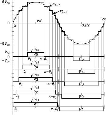
FIGURE 17.2 Output phase voltage waveform of a 11-level cascade inverter with five separate dc sources.
For a stepped waveform such as the one depicted in Fig. 17.2 with s steps, the Fourier transform for this waveform follows [14, 18]
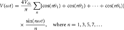 (17.1)
From Eq. (17.1), the magnitudes of the Fourier coefficients when normalized with respect to Vdc are as follows
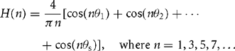 (17.2)
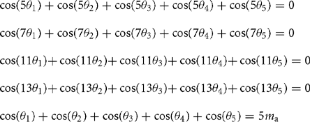
The conducting angles, θ1, θ2, …, θs, can be chosen such that the voltage total harmonic distortion is minimum. Generally, these angles are chosen so that predominant lower frequency harmonics, 5, 7, 11, and 13 are eliminated [19]. More details on harmonic elimination techniques will be discussed in the following section.
Multilevel cascaded inverters have been proposed for such applications as static var generation, an interface with renewable energy sources, and for battery-based applications.
Three-phase cascaded inverters can be connected in wye, as shown in Fig. 17.3, or in delta. Peng et al. has demonstrated a prototype multilevel cascaded static var generator connected in parallel with an electrical system that could supply or draw reactive current from an electrical system [20–23]. The inverter could be controlled to regulate either the power factor of the current drawn from the source or the bus voltage of the electrical system where the inverter was connected. Peng et al.[20] and Joos et al. [24] have also shown that a cascade inverter can be directly connected in series with the electrical system for static var compensation. Cascaded inverters are ideal for connecting renewable energy sources with an ac grid because of the need for separate dc sources in applications such as photovoltaics or fuel cells.
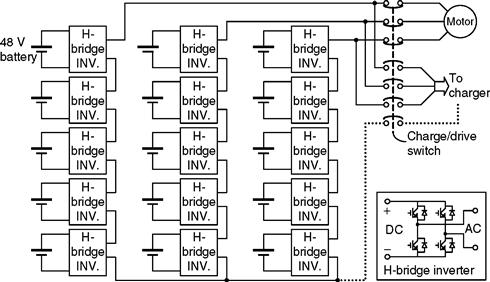
FIGURE 17.3 Three-phase wye-connection structure for electric vehicle motor drive and battery charging.
Cascaded inverters have also been proposed for use as the main traction drive in electric vehicles where several batteries or ultracapacitors are well suited to serve as SDCSs [18, 25]. The cascaded inverter could also serve as a rectifier or charger for the batteries of an electric vehicle while the vehicle was connected to an ac supply as shown in Fig. 17.3. In addition, the cascade inverter can act as a rectifier in a vehicle that uses regenerative braking.
Manjrekar and Lipo have proposed a cascade topology that uses multiple dc levels, which instead of being identical in value are multiples of each other [26, 27]. They also used a combination of fundamental frequency switching for some of the levels and PWM switching for part of the levels to achieve the output voltage waveform. This approach enables a wider diversity of output voltage magnitudes; however, it also results in unequal voltage and current ratings for each of the levels and loses the advantage of being able to use identical modular units for each level.
The main advantages and disadvantages of multilevel cascaded H-bridge converters are as follows [28, 29].
17.2.1.2 Disadvantages
• Separate dc sources are required for each of the H-bridges. This will limit its application to products that already have multiple SDCSs readily available.
Another kind of cascaded multilevel converter with transformers using standard three-phase bi-level converters has been proposed [14]. The circuit is shown in Fig. 17.4. The converter uses output transformers to add different voltages. In order to add up the converter output voltages, the outputs of the three converters need to be synchronized with a separation of 120° between each phase. For example, for obtaining a three-level voltage between outputs a and b, the output voltage can be synthesized by Vab = Va1–b1 + Vb1–a2 + Va2–b2. An isolated transformer is used to provide voltage boost. With three converters synchronized, the voltages, Va1–b1, Vb1–a2, Va2–b2, are all in phase, and thus, the output level can be tripled [1].
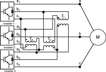
FIGURE 17.4 Cascaded multilevel converter with transformers using standard three-phase bi-level converters.
The advantage of the cascaded multilevel converters with transformers using standard three-phase bi-level converters is that the three converters are identical, and thus, control is more simple. However, the three converters need separate dc sources, and a transformer is needed to add up the output voltages.
17.2.2 Diode-Clamped Multilevel Inverter
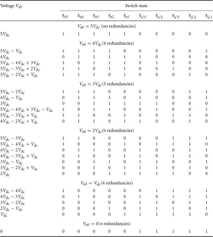
The neutral point converter proposed by Nabae, Takahashi, and Akagi in 1981 was essentially a three-level diode-clamped inverter [5]. In the 1990s, several researchers published articles that have reported experimental results for four-, five-, and six-level diode-clamped converters for uses such as static var compensation, variable speed motor drives, and high-voltage system interconnections [17–30]. A three-phase six-level diode-clamped inverter is shown in Fig. 17.5. Each of the three phases of the inverter shares a common dc bus, which has been subdivided by five capacitors into six levels. The voltage across each capacitor is Vdc, and the voltage stress across each switching device is limited to Vdc through the clamping diodes. Table 17.1 lists the output voltage levels possible for one phase of the inverter with the negative dc rail voltage Vo as a reference. State condition 1 means the switch is on, and 0 means the switch is off. Each phase has five complementary switch pairs such that turning on one of the switches of the pair requires the other complementary switch to be turned off. The complementary switch pairs for phase leg a are (Sa1, Sa′ 1), (Sa2, Sa′ 2), (Sa3, Sa′ 3), (Sa4, Sa′ 4), and (Sa5, Sa′ 5). Table 17.1 also shows that in a diode-clamped inverter, the switches that are on for a particular phase leg are always adjacent and in series. For a six-level inverter, a set of five switches should be on at any given time.
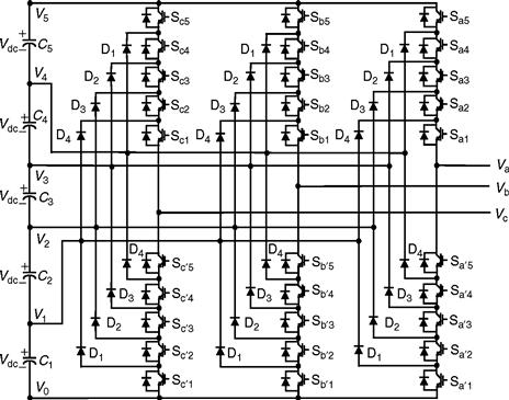
FIGURE 17.5 Three-phase six-level structure of a diode-clamped inverter.
TABLE 17.1 Diode-clamped six-level inverter voltage levels and corresponding switch states
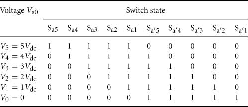
Figure 17.6 shows one of the three line–line voltage waveforms for a six-level inverter. The line voltage Vab consists of a phase-leg “a” voltage and a phase-leg “b” voltage. The resulting line voltage is a 11 -level staircase waveform. This means that an m-level diode-clamped inverter has an m-level output phase voltage and a (2m –l)-level output line voltage.
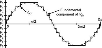
FIGURE 17.6 Line voltage waveform for a six-level diode-clamped inverter.
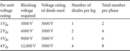
Although each active switching device is required to block only a voltage level of Vdc, the clamping diodes require different ratings for reverse voltage blocking. Using phase a of Fig. 17.5 as an example, when all the lower switches Sa′ 1 through Sa′ 5 are turned on, D4 must block four voltage levels, or 4Vdc. Similarly, D3 must block 3Vdc, D2 must block 2Vdc, and D1 must block Vdc. If the inverter is designed such that each blocking diode has the same voltage rating as the active switches, Dn will require n diodes in series; consequently, the number of diodes required for each phase would be (m –1) × (m –2). Thus, the number of blocking diodes is quadratically related to the number of levels in a diode-clamped converter [28].
One application of the multilevel diode-clamped inverter is an interface between a high-voltage dc transmission line and an ac transmission line [29]. Another application would be a variable speed drive for high-power medium-voltage (2.4–13.8 kV) motors as proposed in [3, 6, 19, 28–30]. Several authors have proposed for the diode-clamped converter that static var compensation is an additional function. The main advantages and disadvantages of multilevel diode-clamped converters are as follows [1–3].
17.2.2.1 Advantages
• All the phases share a common dc bus, which minimizes the capacitance requirements of the converter. For this reason, a back-to-back topology is not only possible but also practical for uses such as a high-voltage back-to-back interconnection or an adjustable speed drive.
17.2.2.2 Disadvantages
• Real-power flow is difficult for a single inverter because the intermediate dc levels will tend to overcharge or discharge without precise monitoring and control.
• The number of clamping diodes required is quadratically related to the number of levels, which can be cumbersome for units with a high number of levels.
17.2.3 Flying-Capacitor Multilevel Inverter
Meynard and Foch introduced a flying-capacitor-based inverter in 1992 [31]. The structure of this inverter is similar to that of the diode-clamped inverter except that instead of using clamping diodes, the inverter uses capacitors. The circuit topology of the flying-capacitor multilevel inverter is shown in Fig. 17.7. This topology has a ladder structure of dc side capacitors, where the voltage on each capacitor differs from that of the next capacitor. The voltage increment between two adjacent capacitor legs gives the size of the voltage steps in the output waveform.
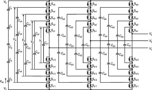
FIGURE 17.7 Three-phase six-level structure of a fly ing-capacitor inverter.
One advantage of the flying-capacitor-based inverter is that it has redundancies for inner voltage levels, that is, in other words, two or more valid switch combinations can synthesize an output voltage. Table 17.2 shows a list of all the combinations of phase voltage levels that are possible for the six-level circuit shown in Fig. 17.7. Unlike the diode-clamped inverter, the flying-capacitor inverter does not require all of the switches that are “on” (conducting) be in a consecutive series. Moreover, the flying-capacitor inverter has “phase” redundancies, whereas the diode-clamped inverter has only “line-line” redundancies [2, 3, 32]. These redundancies allow a choice of charging or discharging specific capacitors and can be incorporated in the control system for balancing the voltages across the various levels.
TABLE 17.2 Flying-capacitor six-level inverter redundant voltage levels and corresponding switch states
In addition to the (m –1) dc link capacitors, the m-level flying-capacitor multilevel inverter will require (m –1) × (m –2)/2 auxiliary capacitors per phase if the voltage rating of the capacitors is identical to that of the main switches. One application proposed in the literature for the multilevel flying capacitor is static var generation [2, 3]. The main advantages and disadvantages of multilevel flying-capacitor converters are as follows [2, 3].
17.2.3.2 Disadvantages
• Control is complicated to track the voltage levels for all of the capacitors. Also, precharging all of the capacitors to the same voltage level and start-up are complex.
• Switching utilization and efficiency are poor for real-power transmission.
• The large number of capacitors are both more expensive and bulky than clamping diodes in multilevel diode-clamped converters. Packaging is also more difficult in inverters with a high number of levels.
17.2.4 Other Multilevel Inverter Structures
Besides the three basic multilevel inverter topologies discussed earlier, other multilevel converter topologies have been proposed; however, most of these are “hybrid” circuits that are combinations of two of the basic multilevel topologies or slight variations to them. In addition, the combination of multilevel power converters can be designed to match with a specific application based on the basic topologies. In the interest of completeness, some of these will be identified and briefly described.
17.2.4.1 Generalized Multilevel Topology
Existing multilevel converters such as diode-clamped and capacitor-clamped multilevel converters can be derived from the generalized converter topology called P2 topology proposed by Peng [33] as shown in Fig. 17.8. The generalized multilevel converter topology can balance each voltage level by itself regardless of load characteristics, active or reactive power conversion, and without any assistance from other circuits at any number of levels automatically. Thus, the topology provides a complete multilevel topology that embraces the existing multilevel converters in principle.
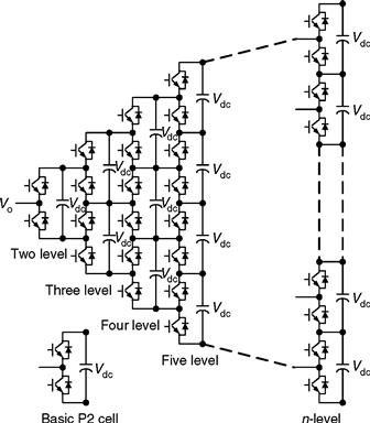
FIGURE 17.8 Generalized P2 multilevel converter topology for one phase leg.
Figure 17.8 shows the P2 multilevel converter structure per phase leg. Each switching device, diode, or capacitor's voltage is 1Vdc, for instance, 1/(m –1) of the dc-link voltage. Any converter with any number of levels, including the conventional bi-level converter, can be obtained using this generalized topology [1, 33].
17.2.4.2 Mixed-Level Hybrid Multilevel Converter
To reduce the number of separate dc sources for high-voltage, high-power applications with multilevel converters, diode-clamped or capacitor-clamped converters can be used to replace the full-bridge cell in a cascaded converter [34]. An example is shown in Fig. 17.9. The nine-level cascade converter incorporates a three-level diode-clamped converter as the cell. The original cascaded H-bridge multilevel converter requires four separate dc sources for one phase leg and 12 for a three-phase converter. If a five-level converter replaces the full-bridge cell, the voltage level is effectively doubled for each cell. Thus, to achieve the same nine voltage levels for each phase, only two separate dc sources are needed for one phase leg and six for a three-phase converter. The configuration has mixed-level hybrid multilevel units because it embeds multilevel cells as the building block of the cascade converter. The advantage of the topology is it needs less separate dc sources. The disadvantage for the topology is its control will be complicated due to its hybrid structure.
FIGURE 17.9 Mixed-level hybrid unit configuration using the three-level diode-clamped converter as the cascaded converter cell to increase the voltage levels.
17.2.4.3 Soft-Switched Multilevel Converter
Some soft-switching methods can be implemented for different multilevel converters to reduce the switching loss and to increase efficiency. For the cascaded converter, because each converter cell is a bi-level circuit, the implementation of soft switching is not at all different from that of conventional bi-level converters. For capacitor-clamped or diode-clamped converters, soft-switching circuits have been proposed with different circuit combinations. One of the soft-switching circuits is a zero-voltage-switching type that includes auxiliary resonant commutated pole (ARCP), coupled inductor with zero-voltage transition (ZVT), and their combinations [1, 35] as shown in Fig. 17.10.
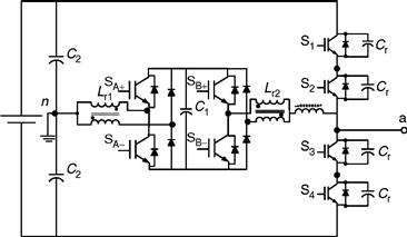
FIGURE 17.10 Zero-voltage-switching capacitor-clamped inverter circuit.
17.2.4.4 Back-to-Back Diode-Clamped Converter
Two multilevel converters can be connected in a back-to-back arrangement, and then the combination can be connected to the electrical system in a series–parallel arrangement as shown in Fig. 17.11. Both the current demanded from the utility and the voltage delivered to the load can be controlled at the same time. This series–parallel active-power filter has been referred to as a universal power conditioner [36–42] when used on electrical distribution systems and as a universal power flow controller [43–47] when applied at the transmission level. Earlier, Lai and Peng [29] proposed the back-to-back diode-clamped topology shown in Fig. 17.12 for use as a high-voltage dc interconnection between two asynchronous ac systems or as a rectifier or inverter for an adjustable speed drive for high-voltage motors. The diode-clamped inverter has been chosen over the other two basic multilevel circuit topologies for use in a universal power conditioner for the following reasons:
• All six phases (three on each inverter) can share a common dc link. Conversely, the cascade inverter requires that each dc level to be separate, and this is not conducive to a back-to-back arrangement.
• The multilevel flying-capacitor converter also shares a common dc link; however, each phase leg requires several additional auxiliary capacitors. These extra capacitors would add substantially to the cost and the size of the conditioner.
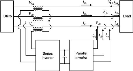
FIGURE 17.11 Series-parallel connection to electrical system of two back-to-back inverters.
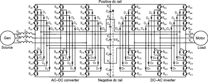
FIGURE 17.12 Six-level diode-clamped back-to-back converter structure.
Because a diode-clamped converter acting as a universal power conditioner will be expected to compensate for harmonics and/or operate in low-amplitude modulation index regions, a more sophisticated higher frequency switch control than the fundamental frequency switching method will be needed. For this reason, multilevel space vector and carrier-based PWM approaches are compared in the next section, as well as novel carrier-based PWM methodologies.
17.3 Multilevel Converter PWM Modulation Strategies
Pulse width modulation strategies used in a conventional inverter can be modified to use in multilevel converters. The advent of the multilevel converter PWM modulation methodologies can be classified according to switching frequency as shown in Fig. 17.13. The three multilevel PWM methods most discussed in the literature have been multilevel carrier-based PWM, selective harmonic elimination, and multilevel space vector PWM, which are all extensions of traditional two-level PWM strategies to several levels. Other multilevel PWM methods have been used to a much lesser extent by researchers; therefore, only the three major techniques will be discussed in this chapter.
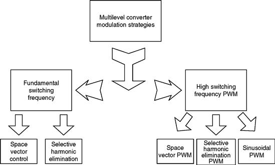
FIGURE 17.13 Classification of PWM multilevel converter modulation strategies.
17.3.1 Multilevel Carrier-Based PWM
Several different two-level, carrier-based PWM techniques have been extended to multiple levels as a means for controlling the active devices in a multilevel converter. The most popular and easiest technique to implement uses several triangle carrier signals and one reference, or modulation, signal per phase. Figure 17.14 illustrates three major carrier-based techniques used in a conventional inverter that can be applied in a multilevel inverter: sinusoidal PWM (SPWM), third harmonic injection PWM (THPWM), and space vector PWM (SVM). SPWM is a very popular method in industrial applications.
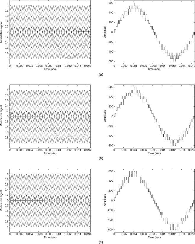
FIGURE 17.14 Simulation of modulation signals and their line-line output voltage using five separate dc sources (60 V for each dc source) cascaded multilevel inverter with three major conventional carrier-based PWM techniques at unity modulation index and 2-kHz switching frequency: (a) SPWM; (b) THPWM; and (c) SVM.
In order to achieve better dc link utilization at high modulation indices, the sinusoidal reference signal can be injected by a third harmonic with a magnitude equal to 25% of the fundamental, its line–line output voltage is shown in Fig. 17.14b. As can be seen in Fig. 17.14b, c, the reference signals have some margin at unity amplitude modulation index. Obviously, the dc utilization of THPWM and SVM are better than SPWM in the linear modulation region. The dc utilization means the ratio of the output fundamental voltage to the dc link voltage. Other interesting carrier-based multilevel PWM are subharmonic PWM (SH-PWM) and switching frequency optimal PWM (SFO-PWM). In addition, some particular aspects of these carrier-based methods are also discussed as follows.
17.3.1.1 Subharmonic PWM
Carrara et al. [48] extended SH-PWM to multiple levels as follows: for an m-level inverter, m –1 carriers with the same frequency fc and the same amplitude Ac are disposed such that the bands they occupy are contiguous. The reference waveform has peak-to-peak amplitude Am, a frequency fm, and its zero centered in the middle of the carrier set. The reference signal is continuously compared with each of the carrier signals. If the reference signal is greater than a carrier signal, then the active device corresponding to that carrier is switched on, and if the reference signal is lesser than a carrier signal, then the active device corresponding to that carrier is switched off.
In multilevel inverters, the amplitude modulation index, ma, and the frequency ratio, mf, are defined as
![]() (17.3)
(17.3)
Figure 17.15 shows a set of carriers (mf = 21) for a six-level diode-clamped inverter and a sinusoidal reference, or modulation waveform, with an amplitude modulation index of 0.8. Figure 17.15 also shows the resulting output voltage of the inverter.
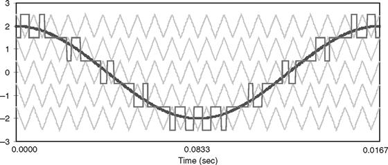
FIGURE 17.15 Multilevel carrier-based SH-PWM showing carrier bands, modulation waveform, and inverter output waveform (m = 6, mf = 21, ma = 0.8).
17.3.1.2 Switching Frequency Optimal PWM
Another carrier-based method that was extended to multilevel applications by Menzies et al. is termed SFO-PWM, and it is similar to SH-PWM except that a zero-sequence (triplen harmonic) voltage is added to each of the carrier waveforms [49]. This method takes the instantaneous average of the maximum and minimum of the three reference voltages (V*a, V*b, V*c) and subtracts this value from each of the individual reference voltages, i.e.
![]() (17.5)
(17.5)
The addition of this triplen-offset voltage centers all of the three reference waveforms in the carrier band, which is equivalent to using space vector PWM [50, 51]. The analog equivalent of Eqs. (17.5–17.8) is shown in Fig. 17.16 [52]. The SFOPWM is shown in Fig. 17.17 for the same reference voltage waveform that was used in Fig. 17.1. The resulting output voltage of the inverter is also shown in Fig. 17.17. The SFOPWM technique enables the modulation index to be increased by 15% before the overmodulation region is reached.
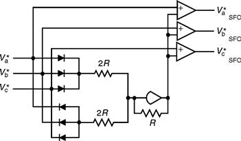
FIGURE 17.16 Analog circuit for zero-sequence addition in SFO-PWM.
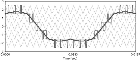
FIGURE 17.17 Multilevel carrier-based SFO-PWM showing carrier bands, modulation waveform, and inverter output waveform (m = 6, mf = 21, ma = 0.8).
For the SH-PWM and SFO-PWM techniques shown in Figs. 17.15 and 17.17, the top and bottom switches are switched much more often than the intermediate devices. Methods to balance or reduce the device switchings without an adverse effect on a multilevel inverter's output voltage total harmonic distortion would be beneficial. The development of such methods is discussed in [53]. A novel method to balance device switchings for all of the levels in a diode-clamped inverter has been demonstrated for SH-PWM and SFO-PWM by varying the frequency for the different triangle wave carrier bands as shown in Fig. 17.18 [53].
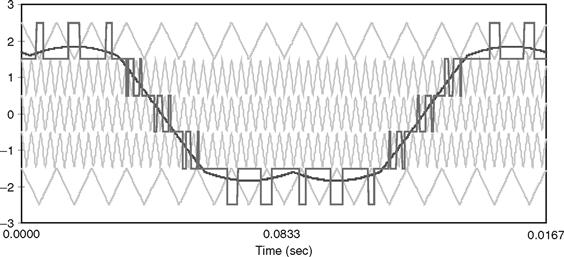
FIGURE 17.18 SFO-PWM where carriers have different frequencies (ma = 0.85, mf = 15 for Band2, Band–2; mf = 55 for Band1, Band–1; Band0, ϕ = 0.10 rad).
17.3.1.3 Modulation Index Effect on Level Utilization
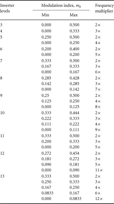
For low-amplitude modulation indices, a multilevel inverter will not make use of all of its levels, and at very low modulation indices, it operates as if it is a traditional two-level inverter. Figure 17.19 shows two simulation results of what the output voltage waveform looks like at amplitude modulation indices of 0.5 and 0.15. Figure 17.19a shows how the bottom and top switches (Sa1 –Sa′ 1, Sa5 –Sa′ 5 in Fig. 17.5) are unused for amplitude modulation indices less than 0.6 in a six-level inverter. Figure 17.19b shows how only the middle switches (Sa3 –Sa′ 3 in Fig. 17.5) change states when a six-level inverter is operated at an amplitude modulation index less than 0.2. The output waveform in Fig. 17.19b appears to be that of a traditional two-level inverter rather than a multilevel inverter.
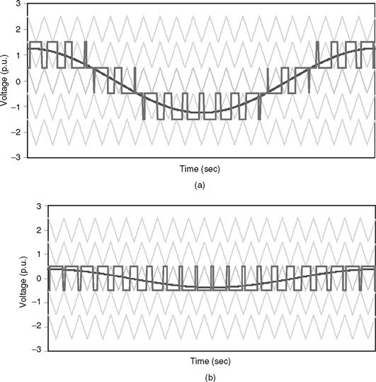
FIGURE 17.19 Level reduction in a six-level inverter at low modulation indices: (a) SH-PWM, m = 6, ma = 0.5 and (b) SH-PWM, m = 6, ma = 0.15.
The minimum modulation index ma min, for which a multilevel inverter controlled with SH-PWM makes use of all of its levels, m, is
![]() (17.9)
(17.9)
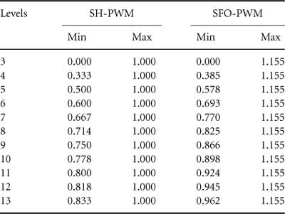
Table 17.3 lists the minimum modulation index in which a multilevel inverter uses all its constituent levels for both SH-PWM and SFO-PWM techniques. Table 17.3 also shows that the maximum modulation index before pulse dropping (overmodulation) occurs is 1.000 for SH-PWM and 1.155 for SFO-PWM. As shown in Table 17.3, when a multilevel inverter operates at modulation indices much less than 1.000, not all of its levels are involved in the generation of the output voltage and simply remain in an unused state until the modulation index increases sufficiently. The table also shows that level usage is more likely to suffer to a greater extent as the number of levels in the inverter increases.
TABLE 17.3 Modulation index ranges without level reduction (min) or pulse dropping because of overmodulation (max)
One way to make use of the multiple levels, even during low modulation periods, is to take advantage of the redundant output voltage states by rotating level usage in the inverter after each modulation cycle. This will reduce the switching stresses on some of the inner levels by making use of those outer voltage levels that otherwise would go unused.
As mentioned earlier, diode-clamped inverters have redundant line–line voltage states for low modulation indices but have no phase redundancies [54]. For an output voltage state (i, j, k) in an m-level diode-clamped inverter, the number of redundant states available is given by
![]() (17.10)
(17.10)
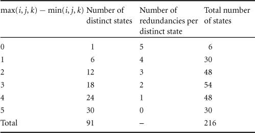
As the modulation index decreases, more redundant states are available. Table 17.4 shows the number of distinct and redundant line–line voltage states available in a six-level inverter for different output voltages.
TABLE 17.4 Six-level inverter line-line voltage redundancies
In the next section, a carrier-based method is given that uses line–line redundancies in a diode-clamped inverter operating at a low modulation index so that active device usage is more balanced among the levels.
17.3.1.4 Increasing Switching Frequency at Low Modulation Indices
For amplitude modulation indices less than 0.5, the level usage in odd-level inverters can be sufficiently rotated so that the switching frequency can be doubled and still keep the thermal losses within the limits of the device. For inverters with an even number of levels, the modulation index at which frequency doubling can be accomplished varies with the levels as shown in Table 17.5. This increase in switching frequency enables the inverter to compensate for higher frequency harmonics and yields a waveform that more closely tracks a reference.
TABLE 17.5 Increased switching frequency possible at lower modulation indices
As an example of how to accomplish this doubling of inverter frequency, an analysis of a seven-level diode-clamped inverter with an amplitude modulation index of 0.4 is conducted. During the first cycle, the reference waveform is centered in the upper three carrier bands, and during the next cycle, the reference waveform is centered in the lower three carrier bands as shown in Fig. 17.20. This technique enables half of the switches to “rest” every other cycle and does not incur any switching losses. With this method, the switching frequency (or carrier frequency fc in the case of multilevel inverters) can effectively be doubled to 2fc, but the switches will have the same thermal losses as if they were switching at fc but every cycle.
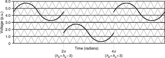
FIGURE 17.20 Reference rotation among carrier bands at low modulation indices (ma < 0.5).
This method is possible only for three-wire systems because the diode-clamped inverter has line–line redundancies and no phase redundancies. This means that at the discontinuity where the reference moves from one carrier band set to another, the transition has to be synchronized such that all three phases are moved from one carrier set to the next set at the same time. In the case of frequency doubling, all three phases add or subtract the following number of states (or levels) every other reference cycle
![]() (17.11)
(17.11)
At modulation indices closer to zero, the switching frequency can be increased even more. This is possible because the reference waveform can be rotated among the carrier bands for a few cycles before returning to a previous set of switches for use. The switches are allowed to “rest” for a few cycles and thus are able to absorb higher losses during the cycle they are switched. Table 17.5 shows the possible increased switching frequencies available at lower amplitude modulation indices for several different inverter levels.
Some additional switching loss is associated with the redundant switchings of the three phases at the end of each modulation cycle when rotating among carrier bands. For instance, for Fig. 17.20, each of the three phases in the seven-level inverter will have three switch pairs that change states at the end of every reference cycle. However, compared with the switching loss associated with just the normal PWM switchings, this redundant switching loss is quite small, typically less than 5% of the total switching loss.
Figures 17.21 and 17.22 show two different methods of rotating the reference waveform among three different regions (top, middle, and bottom) for modulation indices less than 0.333 in a seven-level inverter to enable the carrier frequency to be increased by a factor of three. The method shown in Fig. 17.21 is preferred over that shown in Fig. 17.22 because of less redundant state switching. The method shown in Fig. 17.21 requires only four redundant state switchings for every three reference cycles, whereas the method shown in Fig. 17.22 requires eight redundant switchings for every three reference cycles. In general for any multilevel inverter regardless of the number of levels or number of rotation regions, using the preferred reference rotation method will have half of the redundant switching losses that the alternate method would have.
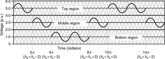
FIGURE 17.21 Preferred method of reference rotation among carrier bands with 3× carrier frequency at very low modulation indices.
FIGURE 17.22 Alternate method of reference rotation among carrier bands with 3× carrier frequency at very low modulation indices.
Unlike the diode-clamped inverter, the cascaded H-bridge inverter has phase redundancies in addition to the aforementioned line–line redundancies. Phase redundancies are much easier to exploit than line–line redundancies because the output voltage in each phase of a three-phase inverter can be generated independently of the other two phases when only phase redundancies are used. A method was given in [18] that makes use of these phase redundancies in a cascaded inverter so that duty cycle of each active device is balanced over (m –l)/2 modulation waveform cycles regardless of the modulation index. The same pulse rotation technique used for fundamental frequency switching of cascade inverters was used but with a PWM output voltage waveform [55], which is a much more effective means of controlling a driven motor at low speeds than continuing to do fundamental frequency switching. The effect of this control is that the output waveform can have a high switching frequency, but the individual levels can still switch at a constant switching frequency of 60 Hz if desired.
17.3.2 Multilevel Space Vector PWM
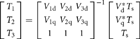
Choi et al. [56] was the first author to extend the two-level space vector PWM technique to more than three levels for the diode-clamped inverter. Figure 17.23 shows how the space vector d–q plane looks like for a six-level inverter. Figure 17.24 represents the equivalent dc link of a six-level inverter as a multiplexer that connects each of the three output phase voltages to one of the dc linkvoltage tap points [57]. Each integral point on the space vector plane represents a particular three-phase output voltage state of the inverter. For instance, the point (3, 2, 0) on the space vector plane means, that with respect to ground, “a” phase is at 3Vdc, “b” phase is at 2Vdc, and “c” phase is at 0Vdc. The corresponding connections between the dc link and the output lines for the six-level inverter are also shown in Fig. 17.24 for the point (3, 2, 0). An algebraic way to represent the output voltages in terms of the switching states and dc link capacitors is described in the following [58]. For n = m –1, where m is the number of levels in the inverter,
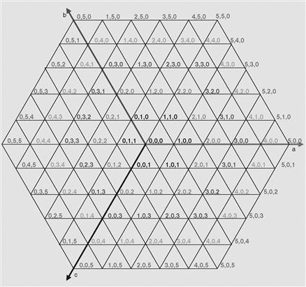
FIGURE 17.23 Voltage space vectors for a six-level inverter.
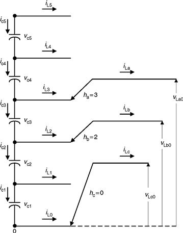
FIGURE 17.24 Multiplexer model of diode-clamped six-level inverter.
![]() (17.12)
(17.12)
![]()
and
where ha is the switch state and j is an integer from 0 to n, and where δ(x) = 1 if x ≥ 0, δ(x) = 0 if x < 0.
Besides the output voltage state, the point (3, 2, 0) on the space vector plane can also represent the switching state of the converter. Each integer indicates how many upper switches in each phase leg are on for a diode-clamped converter. As an example, for ha = 3, hb, = 2, hc = 0, the Habc matrix for this particular switching state of a six-level inverter would be
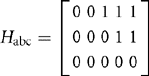
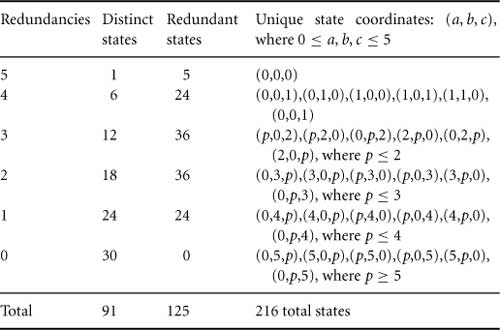
Redundant switching states are those states for which a particular output voltage can be generated by more than one switch combination. Redundant states are possible at lower modulation indices or at any point other than those on the outermost hexagon shown in Fig. 17.23. Switch state (3, 2, 0) has redundant states (4, 3, 1) and (5, 4, 2). Redundant switching states differ from each other by an identical integral value, i.e. (3, 2, 0) differs from (4, 3, 1) by (1, 1, 1) and from (5, 4, 2) by (2, 2, 2).
For an output voltage state (x, y, z) in an m-level diode-clamped inverter, the number of redundant states available is given by m –1 –max(x, y, z). As the modulation index decreases (or the voltage vector in the space vector plane gets closer to the origin), more redundant states are available. The number of possible zero states is equal to the number of levels, m. For a six-level diode-clamped inverter, the zero-voltage states are (0, 0, 0), (1, 1, 1), (2, 2, 2), (3, 3, 3), (4, 4, 4), and (5,5,5).
The number of possible switch combinations is equal to the cube of the level (m3). For this six-level inverter, there are 216 possible switching states. The number of distinct or unique states for an m-level inverter can be given by
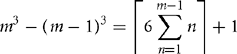 (17.13)
Therefore, the number of redundant switching states for an m-level inverter is (m –1)3. Table 17.6 summarizes the available redundancies and distinct states for a six-level diode-clamped inverter.
TABLE 17.6 Line–line redundancies of six-level three-phase diode-clamped inverter
In two-level PWM, a reference voltage is tracked by selecting the two nearest voltage vectors and a zero vector, and then by calculating the time required to be at each of these three vectors such that their sum equals the reference vector. In multilevel PWM, generally the nearest three triangle vertices, V1, V2, and V3, to a reference point V* are selected to minimize the harmonic components of the output line–line voltage [59]. The respective time duration, T1, T2, and T3, required for these vectors is then solved from the following equations
![]() (17.14)
(17.14)
where Ts is the switching period. Equation (17.14) actually represents two equations, one with the real part of the terms and one with the imaginary part of the terms
![]() (17.16)
(17.16)
Equations (17.15) –(17.18) can then be solved for T1, T2, and T3 as follows:
 (17.18)
Others have proposed space vector methods that did not use the nearest three vectors, but these methods generally add complexity to the control algorithm. Figure 17.25 shows what a sinusoidal reference voltage (circle of points) and the inverter output voltages look like in the d–q plane.
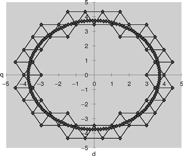
FIGURE 17.25 Sinusoidal reference and inverter output voltage states in d–q plane.
Redundant switch levels can be used to help manage the charge on the dc link capacitors [60]. Generalizing from Fig. 17.24, the equations for the currents through the dc link capacitors can be given as
![]() (17.19)
(17.19)
and
![]() (17.20)
(17.20)
The dc link currents for ha = 3, hb, = 2, hc = 0 would be ic5 = ic4 = 0, ic3 = –ia, ic2 = –ia. –ib, ic1 = –ia –ib.To see how redundant states affect the dc link currents, consider the two redundant states for (3, 2, 0). In state (4, 3, 1), the dc link currents would be ic5 = ic4 = –ia, ic3 = –ia –ib, ic2 = –ia –ib, ic1 = –ia –ib –ic = 0; and for the state (5, 4, 2), the dc link currents would be ic5 = –ia, ic4 = –ia, ib, ic3 = –ia –ib, ic2 = –ic1 –ia, –ib = –ic = 0
From this example, one can see that the choice of redundant switching states can be used to determine which capacitors will be charged/discharged or unaffected during the switching period. Although this control is helpful in balancing the individual dc voltages across the capacitors that make up the dc link, this method is quite complicated in selecting which of the redundant states to use. Constant use of redundant switching states also results in a higher switching frequency and lower efficiency of the inverter because of the extra switchings. Optimized space vector switching sequences for multilevel inverters have been proposed in [61].
17.3.3 Selective Harmonic Elimination
17.3.3.1 Fundamental Switching Frequency
The selective harmonic elimination method is also called fundamental switching frequency method based on the harmonic elimination theory proposed by Patel and Hoft [62, 63]. A typical 11-level multilevel converter output with fundamental frequency switching scheme is shown in Fig. 17.2. The Fourier series expansion of the output voltage waveform as shown in Fig. 17.2 is expressed in Eqs. (17.1) and (17.2).
The conducting angles, θ1, θ2, …, θs, can be chosen such that the voltage total harmonic distortion is a minimum. Normally, these angles are chosen so as to cancel the predominant lower frequency harmonics [19].
For the 11-level case in Fig. 17.2, the 5th, 7th, 11th, and 13th harmonics can be eliminated with the appropriate choice of the conducting angles. One degree of freedom is used so that the magnitude of the fundamental waveform corresponds to the reference waveform's amplitude or modulation index, ma, which is defined as V*L/VLmax. V*L is the amplitude command of the inverter for a sine wave output phase voltage, and VLmax is the maximum attainable amplitude of the converter, i.e. VLmax = s · Vdc. The equations from Eq. (17.2) will now be as follows
 (17.21)
The above equations are nonlinear transcendental equations that can be solved by an iterative method such as the Newton-Raphson method. For example, using a modulation index of 0.8 obtains the following: θ1 = 6.57°, θ2 = 18.94°, θ3 = 27.18°, θ4 = 45.14°, θ5 = 62.24°. Thus, if the inverter output is symmetrically switched during the positive half cycle of the fundamental voltage to +Vdc at 6.57°, + 2Vdc at 18.94°, + 3Vdc at 27.18°, + 4Vdc at 45.14°, and + 5Vdc at 62.24° and similarly in the negative half cycle to –Vdc at 186.57°, –2Vdc at 198.94°, –3Vdc at 207.18°, –4Vdc at 225.14°, –5Vdc at 242.24°, the output voltage of the 11-level inverter will not contain the 5th, 7th, 11th, and 13th harmonic components [18]. Other methods to solve these equations include using genetic algorithms [64] and resultant theory [65–67].
Practically, the precalculated switching angles are stored as the data in memory (look-up table). Therefore, a microcontroller could be used to generate the PWM gate drive signals.
17.3.3.2 Selective Harmonic Elimination PWM
In order to achieve a wide range of modulation indexes with minimized THD for the synthesized waveforms, a generalized selective harmonic modulation method [68, 69] was proposed, which is called virtual stage PWM [64]. An output waveform is shown in Fig. 17.26. The virtual stage PWM is a combination of the unipolar programmed PWM and the fundamental frequency switching scheme. The output waveform of unipolar programmed PWM is shown in Fig. 17.27. When unipolar programmed PWM is employed on a multilevel converter, typically one dc voltage is involved, where the switches connected to the dc voltage are switched “on” and “off” several times per fundamental cycle. The switching pattern decides what the output voltage waveform looks like.
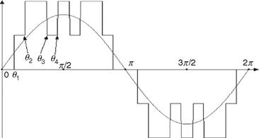
FIGURE 17.26 Output waveform of virtual stage PWM control.
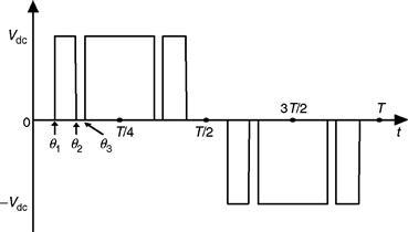
FIGURE 17.27 Unipolar switching output waveform.
For fundamental switching frequency method, the number of switching angles is equal to the number of dc sources. However, for the virtual stage PWM method, the number of switching angles is not equal to the number of dc voltages. For example, in Fig. 17.26, only two dc voltages are used, whereas there are four switching angles.
Bipolar programmed PWM and unipolar programmed PWM could be used for modulation indices too low for the applicability of the multilevel fundamental frequency switching method. Virtual stage PWM can also be used for low modulation indices. Virtual stage PWM will produce output waveforms with a lower THD most of the time [64]. Therefore, virtual stage PWM provides another alternative to bipolar programmed PWM and unipolar programmed PWM for low modulation index control.
The major difficulty for selective harmonic elimination methods, including the fundamental switching frequency method and the virtual stage PWM method, is to solve the transcendental Eq. (17.21) for switching angles. Newton's method can be used to solve Eq. (17.21), but it needs good initial guesses, and solutions are not guaranteed. Therefore, Newton's method is not feasible to solving equations for large number of switching angles if good initial guesses are not available [70].
Recently, the resultant method has been proposed in [65–67] to solve the transcendental equations for switching angles. The transcendental equations characterizing the harmonic content can be converted into polynomial equations. Elimination resultant theory has been employed to determine the switching angles to eliminate specific harmonics, such as the 5th, 7th, 11th, and 13th. However, as the number of dc voltages or the number of switching angles increases, the degrees of the polynomials in these equations become bulky.
To overcome this problem, the fundamental frequency switching angle computation is solved by Newton's method. The initial guess can be provided by the results of lower order transcendental equations by the resultant method [70].
17.4 Multilevel Converter Design Example
The objective of this section is to give a general idea how to design a multilevel converter in a specific application. Different applications for multilevel converters might have different specification requirements. Therefore, the multilevel universal power conditioner (MUPC) is utilized to demonstrate as the design example in this section.
Multilevel diode-clamped converters can be designed where different levels have unequal voltage and current ratings; however, this approach would lose the advantage of being able to use identical, modular units for each leg of the inverter. The method used in this chapter to specify a back-to-back diode-clamped converter for use as a universal power conditioner is for all voltage levels and legs in each of the two inverters to be the same. (The current ratings in the series inverter may be different than those in the parallel inverter.) This approach also allows the control system to extend the frequency range of the inverter by exploiting the additional voltage redundancies available at lower modulation indices as discussed in [71].
17.4.1 Interface with Electrical System
Figure 17.28 illustrates the proposed electrical system connection topology for two diode-clamped inverters connected back-to-back and sharing a common dc bus. One inverter interfaces with the electrical system by means of a parallel connection through output inductors LPI. The other inverter interfaces with the electrical system through a set of single-phase transformers in a series fashion. The primaries of the transformers are inserted in series with each of the three-phase conductors supplied from a utility. The secondaries of the transformers are connected to an ungrounded wye and to the output of the series inverter. By having two inverters, this arrangement allows both the source voltage and the load current to be compensated independently of each other [71, 72]. With only a single inverter, regulating the load voltage and source current at the same time would not be possible.
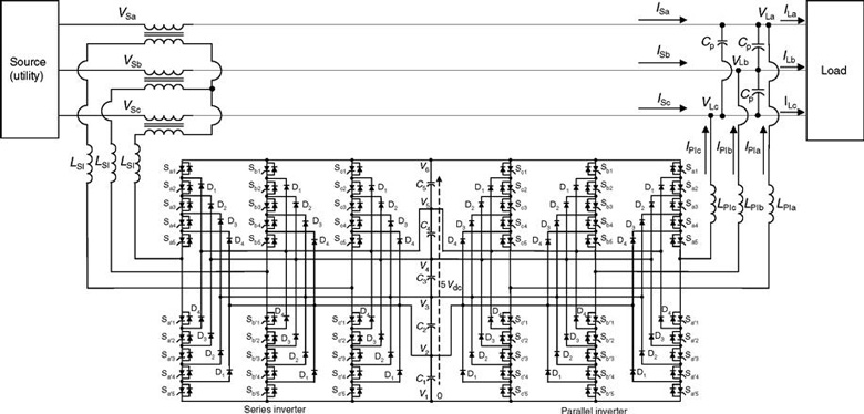
FIGURE 17.28 Electrical system connection of multilevel diode-clamped power conditioner.
The voltage injected into the electrical system by the series inverter compensates for deviations in the source voltage such that a regulated distortion-free waveform is supplied to the load. The parallel inverter injects current into the electrical system to compensate for current harmonics or reactive current demanded by the load such that the current drawn from the utility is in phase with the source voltage and contains no harmonic components.
17.4.2 Number of Levels and Voltage Rating of Active Devices
In a multilevel inverter, determining the number of levels will be one of the most important factors because this affects many of the other sizing factors and control techniques. Tradeoffs, in specifying the number of levels that the power conditioner will need and the advantages and complexity of having multiple voltage levels available, are the primary differences that set a multilevel filter apart from a single-level filter.
The nominal RMS voltage rating, Vnom, of the electrical system is known to which the diode-clamped power conditioner will be connected. The dc link voltage must be at least as high as the amplitude of the nominal line-neutral voltage at the point of connection, or ![]() .
.
The parallel inverter must be able to inject currents by imposing a voltage across the parallel inductors, LPI, which is the difference between the load voltage VL and parallel inverter output voltage VPI. It is difficult to impose a voltage across the inductors when the load voltage waveform is at its maximum or minimum. Simulation results have shown that the amplitude of the desired load voltage Vnom should not be more than 70% of the overall dc link voltage for the parallel inverter to have sufficient margin to inject appropriate compensation currents. Without this margin, complete compensation of reactive currents may not be possible. This margin can be incorporated into a design factor for the inverter. Because the dc link voltage and the voltage at the connection point can vary, the design factor used in the rating selection process incorporates these elements and the small voltage drops that occur in the inverters during active device conduction.
The product of the number of the active devices in series (m –1) and the voltage rating of the devices Vdev must then be such that
![]() (17.22)
(17.22)
The minimum number of levels and the voltage rating of the active devices (IGBTs, GTOs, power MOSFETs, etc.) are inversely related to each other. More levels in the inverter will lower the required voltage device rating of individual devices, or looking at it another way, a higher voltage rating of the devices will enable a fewer minimum number of levels to be used.
Increasing the number of levels does not affect the total voltage blocking capability of the active devices in each phase leg because lower device ratings can be used. Some of the benefits of using more than the minimum required number of levels in a diode-clamped inverter are as follows:
1. Voltage stress across each device is lower. Both active devices and dc link capacitors could be used that have lower voltage ratings (which sometimes are much cheaper and have greater availability).
2. The inverter will have a lower EMI because the dv/dt during each switching will be lower.
3. The output of the waveform will have more steps, or degrees of freedom, which enables the output waveform to closely track a reference waveform.
4. Lower individual device switching frequency will achieve the same results as an inverter with a fewer number of levels and higher device switching frequency. Or the switching frequency can be kept the same as that in an inverter with a fewer number of levels to achieve a better waveform.
The drawbacks of using more than the required minimum number of levels are as follows:
1. Six active device control signals (one for each phase of the parallel inverter and the series inverter) are needed for each hardware level of the inverter, i.e. 6(m –1) control signals. Additional levels require more computational resources and add complexity to the control.
2. If the blocking diodes used in the inverter have the same rating as the active devices, their number increases dramatically because 6(m –2)(m –1) diodes would be required for the back-to-back structure.
Considering the tradeoffs between the number of levels and the voltage rating of the devices will generally lead the designer to choose an appropriate value for each.
17.4.3 Number and Voltage Rating of Clamping Diodes
As mentioned in the previous section, 6(m –1)(m –2) clamping diodes are required for an m-level back-to-back converter if the diodes have the same voltage rating as the active devices. As discussed in Section 17.2, the voltage rating of each series of clamping diodes is designated by the subscript of the diode shown in Fig. 17.28. For instance, D4 must block 4Vdc, D3 must block 3Vdc, and so on.
If diodes that have higher voltage ratings than the active devices are available, then the number of diodes required can be reduced accordingly. When considering diodes of different ratings, the minimum number of clamping diodes per phase leg of the inverter is 2(m –2) and for the complete back-to-back converter is 12(m –2). Unlike the active devices, additional levels do not enable a decrease in the voltage rating of the clamping diodes. In each phase leg, note that the voltage rating of each pair of diodes adds up to the overall dc link voltage (m –1)Vdc. Considering the six-level converter in Fig. 17.28, connected to voltage level V5 are the anode of D1 and the cathode of D4. D1 must be able to block Vdc, and D4 must block 4Vdc; the sum of their voltage blocking capabilities is 5Vdc. For voltage level V4, the anode of D2 and the cathode of D3 are connected together to this point. Again, the sum of their voltage blocking capability is 2Vdc + 3Vdc = 5Vdc. The same is true for the other intermediate voltage levels. Therefore, the total voltage blocking capability per phase of an m-level converter is (m –2)(m –1)Vdc and for the back-to-back converter,
![]() (17.23)
(17.23)
Each additional level added to the converter will require an additional 6(m –1)Vdc in voltage blocking capabilities. From this, one can see that unnecessarily adding more than the required number of voltage levels can quickly become cost prohibitive.
17.4.4 Current Rating of Active Devices
In order to determine the required current rating of the active switching devices for the parallel and series portions of the back-to-back converter shown in Fig. 17.28, the maximum apparent power that each inverter will either supply or draw from the electrical system must be known. These ratings will largely depend on the compensation objectives and on the limits they are specified to maintain. Of the three voltage compensation objectives (voltage sag, unbalanced voltages, voltage harmonics), the greatest power demands of the series inverter will almost always occur during voltage sag conditions. For the parallel inverter, generally the reactive power compensation demands will dominate the design of the converter, as opposed to harmonic current compensation.
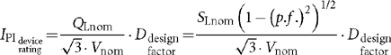
For this analysis, balanced voltage sag conditions will be considered in the specification of the power ratings of the two inverters. A one-line diagram circuit is shown in Fig. 17.29 for the converter and electrical system represented in Fig. 17.28. Equations can be developed for the apparent power required for each of the inverters based on the three phase-rated apparent load power SLnom, rated line–line load voltage VLnom, and line–line source voltage Vs [73].
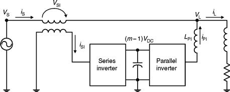
FIGURE 17.29 One-line diagram of a MUPC connected to the electrical system.
17.4.4.1 Series Inverter Power Rating
First, the rating of the series inverter will be considered. The voltage VSI across the series transformer shown in Fig. 17.29, is given by the vector equation
![]() (17.24)
(17.24)
The apparent power delivered from the series converter can then be given as
![]() (17.25)
(17.25)
where the conjugate ![]() is the conjugate of
is the conjugate of ![]() , the source current.
, the source current.
If the load voltage VL is regulated such that it is in phase with the source voltage VS, then Eq. (17.24) can be rewritten as an algebraic equation
![]() (17.26)
(17.26)
Assuming that the back-to-back converter is lossless, the entire real power PL drawn by the load must be supplied by the utility source, PS = PL. If the source current is regulated such that it is in phase with the source voltage, then
![]() (17.27)
(17.27)
Combining Eqs. (17.25)–(17.27), the real power delivered from the series converter is
![]() (17.28)
(17.28)
Multiplying and dividing the right side of Eq. (17.28) by Vs yields
![]() (17.29)
(17.29)
Substituting Eq. (17.27) intoEq. (17.29) provides the following equation for the rated apparent power of the series inverter
![]() (17.30)
(17.30)
Choosing the rated load power SL and the rated load voltage Vl as bases, Fig. 17.30 shows the apparent power SSI in per unit that the series inverter must provide as a function of the source voltage VS. Each of the curves in Fig. 17.30 is for loads of different power factors. As shown in Fig. 17.30, the apparent power that the series inverter has to transfer is proportional to the power factor of the load [73].
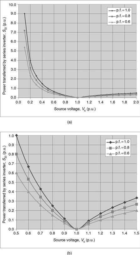
FIGURE 17.30 Apparent power requirements of series inverter during voltage sags.
Figure 17.30a shows that for voltage sags less than 50% of nominal, the series inverter would have to be rated to transfer more power than the rated load power, which in most applications would not be practical. Figure 17.30b shows that for sags that are small in magnitude, the series inverter would have a rating much less than that of the rated load power. For example, for a 20% voltage sag (Vs = 0.8Vnom), the required power rating of the series inverter is only 25% of the rated load.
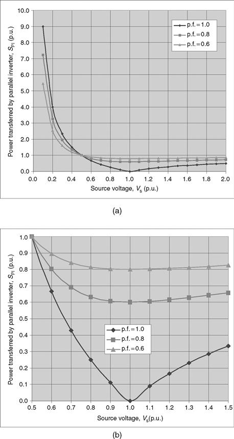
FIGURE 17.31 Apparent power requirements of parallel inverter during voltage sags.
When considering selection of the active devices for the series inverter, as shown in Fig. 17.30, the magnitude of the voltage sag to be compensated will play a large role in determining the current rating required. The formula for determining the current rating of each of the devices as a function of the minimum source voltage to be compensated, min(Vs), is given in Eq. (17.31)
![]() (17.31)
(17.31)
The safety factor, or design factor, in Eq. (17.31) should be chosen to allow for future growth in the load supplied by the utility and compensated by the power conditioner.
17.4.4.2 Parallel Inverter Power Rating
The power rating of the parallel inverter will now be considered. From Fig. 17.29, the apparent power delivered to the electrical system by the parallel inverter can be expressed as
![]() (17.32)
(17.32)
because the source current Is and load voltage VL are controlled such that they are in phase with the source voltage [73]. Multiplying and dividing the second term of Eq. (17.32) by Vs and substituting Eq. (17.27) yields the following
![]() (17.33)
(17.33)
Substituting Eq. (17.33) into Eq. (17.32) and combining like terms yields
![]() (17.34)
(17.34)
Figure 17.31 shows the apparent power SPI in per unit that the parallel inverter must provide as a function of the source voltage Vs for loads of different power factors. Because the power transferred for voltage declines to less than 50% of nominal is predominantly real power, the parallel inverter would have to have an extraordinarily high rating if the conditioner were designed to compensate for such large voltage sags, just like the series inverter. From Fig. 17.31b, one can see that for a voltage sag to 50% of nominal, the parallel inverter has to draw a current IPI equal to that drawn by the rated load IL. However, unlike the series inverter, the dominant factor in determining the power rating of the parallel inverter is the load power factor if the conditioner is designed to compensate for only marginal voltage sags as shown in Fig. 17.3 lb.
If the design of the universal power conditioner is to compensate for voltage sags to less than 50% of nominal voltage, then Eq. (17.31) should be used to determine the current rating of the parallel inverter. If the design of the conditioner is for marginal voltage sags (to 70% of nominal voltage) and the MUPC will be applied to a customer load that has a power factor of less than 0.9, then the following equation is more suited for calculating the current rating of the parallel inverter's active devices
 (17.35)
One common design for the parallel inverter in a universal power conditioner is for the inverter to have a current rating equal to that of the rated load current IL.
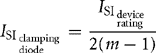
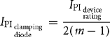
17.4.5 Current Rating of Clamping Diodes
When a multilevel inverter outputs an intermediate voltage level, not 0 or (m –1)Vdc, only one clamping diode in each phase leg conducts current at any instant in time, whereas half of the active switches are conducting at all times. The diode that is conducting current is determined by the intermediate dc voltage level, which is connected to the output phase conductor, and by the direction of the current flow, positive or negative. For instance, when a phase leg of the series inverter in Fig. 17.28 is connected to level V4, diode D2 conducts for current flowing from the inverter to the electrical system, and then diode D3 conducts for current flowing into the inverter from the electrical system.
This example illustrates that for current flowing out of an inverter, only the clamping diodes in the top half of a phase leg will conduct, and for current flowing into an inverter, only the clamping diodes in the bottom half of the phase leg will conduct. In all likelihood, the current waveforms will be odd symmetric. These facts alone enable the average current rating for the clamping diodes to be at most one half that of the active devices. The clamping diodes should all have a pulse or short-time current rating equal to the amplitude of the maximum compensation current that the inverter is expected to conduct. Generally, this is equal to ![]() times the value calculated in Eq. (17.31) or (17.35) for the series and parallel inverters.
times the value calculated in Eq. (17.31) or (17.35) for the series and parallel inverters.
The average current that flows through each clamping diode is dependent on currents is1 and ipi, the modulation index, and the control of the voltage level outputs of the inverter. Because all of these are widely varying attributes in a power conditioner, an explicit formula for determining their ratings would be difficult at best. Nonetheless, for the assumption that each clamping diode conducts an equal amount of current and that each level of the inverter is “on” for an equal duration of time, their average current ratings for the series and parallel inverter could be found from the following equations
 (17.36)
or
 (17.37)
17.4.6 DC Link Capacitor Specifications
Unipolar capacitors can be used for the dc link capacitors. Just like the voltage rating of the active devices in Eq. (17.22), the sum of the voltage ratings of the dc link capacitors should be greater than or equal to the overall dc link voltage, which is equal to the right side of Eq. (17.22). The design factors in this case includes the dc link voltage ripple plus safety factors necessary to maintain the capacitors within their safe operating range.
The capacitance of each capacitor in the dc link is determined by the equation
![]() (17.38)
(17.38)
where n = 1, 2, 3, …, m –1, Δqn is the change in charge, and Vn is the change in voltage over a specified period.
The required capacitance of the dc link and the voltage ripple are inversely related to each other. An increase in the capacitance will decrease the amount of ripple in the dc voltage. By assuming that each level has the same voltage Vdc across it,
![]() (17.39)
(17.39)
Figure 17.32 shows a graph of the required capacitance as a function of the maximum permissible voltage ripple on the dc link. The graph indicates that an unnecessarily strict tolerance on the voltage ripple of the dc bus will result in extraordinarily large capacitor values. For this reason, the maximum voltage ripple is normally chosen to be in the 5–10% range.
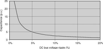
FIGURE 17.32 Capacitance required as a function of the maximum voltage ripple on dc bus.
The current that flows through the capacitor determines the change in charge Δqn for a capacitor Cn. This current is a function of what input and output voltage states the inverter progresses through each cycle and will largely be dependent on the control method implemented by the series and parallel inverter in maintaining the voltage on the dc link. In addition, the current waveforms iPI and iSI also will depend largely on the system conditions, i.e. in other words, the type of compensation that the converter is conducting. Although the current that flows through each capacitor Cn that makes up the dc link will be different, for the reasons mentioned previously in Section 17.4.2, normally each of the capacitors will be identically sized such that Eq. (17.38) can then be rewritten as
![]() (17.40)
(17.40)
Suppose a UPFC is connected to a distribution system with a voltage of 13.8 kV line–line (7970V line–ground). From Eq. (17.22), ![]() .
.
If 3300 V IGBTs are chosen for the design, then the number of levels m would be 6. The next lower rating of available IGBTs is 2500 V, and the use of these devices would require seven levels. Because of the added complexity and computational burden of seven levels, the design with six levels of 3300-V IGBTs is chosen.
A 13.8-kV line–line ac waveform from an inverter requires a minimum dc link voltage of approximately 11.3 kV. The nominal dc voltage for each level would be approximately 2000 V. For a design factor of 1.5, the design voltage for each level of the inverter would be approximately 3000 V.
From Eq. (17.23), the minimum total voltage blocking capability for a back-to-back converter would be Vclamp total = 6(6 –2)(6 –1)3000 V = 360 kV. Each phase of the converter will require the blocking voltages shown in Table 17.7.
TABLE 17.7 Back-to-back MUPC clamping diode ratings
The current rating of the active devices in the series inverter is found from Eq. (17.31)
![]()
The current rating of the active devices in the parallel inverter is found from Eq. (17.35):

Use of 3300 V, 800 A IGBTs would be sufficient for both the series and the parallel inverters.
The current rating of the clamping diodes in the series inverter is found from Eq. (17.36)
![]()
Likewise, the current rating of the clamping diodes in the parallel inverter is found from Eq. (17.37)
![]()
Use of 3000 V, 75 A diodes would be sufficient for both the series and the parallel inverters.
17.5 Fault Diagnosis in Multilevel Converters
Since a multilevel converter is normally used in medium-to high-power applications, the reliability of the multilevel converter system is very important. For instance, industrial drive applications in manufacturing plants are dependent upon induction motors and their inverter systems for process control. Generally, the conventional protection systems are passive devices such as fuses, overload relays, and circuit breakers to protect the inverter systems and the induction motors. The protection devices will disconnect the power sources from the multilevel inverter system whenever a fault occurs, stopping the operated process. Downtime of manufacturing equipment can add up to be thousands or hundreds of thousands of dollars per hour; therefore, fault detection and diagnosis is vital to a company's bottom line. In order to maintain continuous operation for a multilevel inverter system, knowledge of fault behaviors, fault prediction, and fault diagnosis is necessary. Faults should be detected immediately because if a motor drive runs continuously under abnormal conditions, the drive or motor may quickly fail.
The possible structure for a fault diagnosis system is shown in Fig. 17.33. The system is composed of four major states: feature extraction, neural network classification, fault diagnosis, and switching pattern calculation with gate signal output. The feature extraction performs the voltage input signal transformation, with rated signal values as important features, and the output of the transformed signal is transferred to the neural network classification. The networks are trained with both normal and abnormal data for the multilevel inverter drive (MLID); thus, the output of this network is nearly 0 and 1 as binary code. The binary code is sent to the fault diagnosis to decode the fault type and its location. Then, the switching pattern is calculated to reconfigure the multilevel inverter.
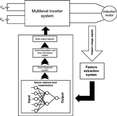
FIGURE 17.33 Structure of fault diagnosis system of a multilevel cascaded H-bridge inverter.
Switching patterns and the modulation index of other active switches can be adjusted to maintain voltage and current in a balanced condition after reconfiguration recovers from a fault. The MLID can continuously operate in a balanced condition; of course, the MLID will not be able to operate at its rated power. Therefore, the MLID can operate in balanced condition at reduced power after the fault occurs until the operator locates and replaces the damaged switch [74].
17.6 Renewable Energy Interface
Multilevel converters can be used to interface with renewable energy or distributed energy resources because several batteries, fuel cells, solar cells, wind turbines, and microturbines can be connected through a multilevel converter to supply a load or the ac grid without voltage balancing problems. Nevertheless, the intrinsic characteristics of renewable energy sources might have some trouble with their energy source utilization; for instance, fuel-cell energy sources have some problems associated with their V–I characteristics. The static V–I characteristic of fuel cells illustrates more than 30% difference in the output voltage between no-load and full-load conditions. This unavoidable decrease, caused by internal losses, reduces fuel-cell utilization factor. Therefore, a multilevel dc–dc converter might be used to overcome the problem as shown in Fig. 17.34. To overcome the fuel-cell voltage drop, either voltage regulators have to be connected at the fuel-cell outputs or fuel-cell voltages have to be monitored and the control signals have to be modified accordingly.
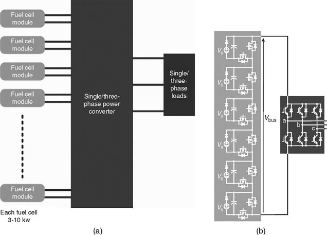
FIGURE 17.34 (a) Block diagram of the multilevel configuration and (b) six-level dc–dc converter connected with three-phase conventional inverter.
Five different approaches for integrating numerous fuel-cell modules have been evaluated and compared with respect to cost, control complexity, ease of modularity, and fault tolerance in [75]. In addition, the optimum fuel-cell utilization technique with a multilevel dc-dc converter has been proposed in [76, 77].
17.7 Conclusion
This chapter has demonstrated the state of the art of multilevel power converter technology. Fundamental multilevel converter structures and modulation paradigms including the pros and cons of each technique have been discussed. Most of the chapter focuses on modern and more practical industrial applications of multilevel converters. A procedure for calculating the required ratings for the active switches, clamping diodes, and dc link capacitors with a design example has been described. The possible future enlargements of multilevel converter technology such as fault diagnosis system and renewable energy sources have been noted. It should be noted that this chapter could not cover all multilevel, power converter–related applications however the basic principles of different multilevel converters have been discussed methodically. The main objective of this chapter is to provide a general notion to readers who are interested in multilevel power converters and their applications.
References
1. Rodriguez J, Lai JS, Peng FZ. Multilevel inverters: survey of topologies, controls, and applications. IEEE Trans. Industry Applications. August 2002; vol. 49(no. 4):724–738.
2. Lai JS, Peng FZ. Multilevel converters –a new breed of power converters. IEEE Trans. Industry Applications. May/June 1996; vol. 32:509–517.
3. Tolbert LM, Peng FZ, Habetler T. Multilevel converters for large electric drives. IEEE Trans. Industry Applications. January/February 1999; vol. 35:36–44.
4. R. H. Baker and L. H. Bannister, “Electric Power Converter,” U.S. Patent 3 867 643, February 1975.
5. Nabae A, Takahashi I, Akagi H. A new neutral-point clamped PWM inverter. IEEE Trans. Industry Applications. September/October 1981; vol. IA-17:518–523.
6. R. H. Baker, “Bridge Converter Circuit,” U.S. Patent 4 270 163, May 1981.
7. P. W. Hammond, “Medium Voltage PWM Drive and Method,” U.S. Patent 5 625 545, April 1977.
8. F. Z. Peng and J. S. Lai, “Multilevel Cascade Voltage-source Inverter with Separate DC Source,” U.S. Patent 5 642 275, June 24, 1997.
9. P. W. Hammond, “Four-quadrant AC-AC Drive and Method,” U.S. Patent 6 166 513, December 2000.
10. M. F. Aiello, P. W. Hammond, and M. Rastogi, “Modular Multi-level Adjustable Supply with Series Connected Active Inputs,” U.S. Patent 6 236 580, May 2001.
11. M. F. Aiello, P. W. Hammond and M. Rastogi, “Modular MultiLevel Adjustable Supply with Parallel Connected Active Inputs,” U.S. Patent 6 301 130, October 2001.
12. J. P. Lavieville, P. Carrere, and T. Meynard, “Electronic Circuit for Converting Electrical Energy and a Power Supply Installation Making Use Thereof,” U.S. Patent 5 668 711, September 1997.
13. T. Meynard, J.-P. Lavieville, P. Carrere, J. Gonzalez and O. Bethoux, “Electronic Circuit for Converting Electrical Energy,” U.S. Patent 5 706 188, January 1998.
14. Cengelci E, Sulistijo SU, Woom BO, Enjeti P, Teodorescu R, Blaabjerg F. A new medium voltage PWM inverter topology for adjustable speed drives. In: Conf. Rec., IEEE Industry Applications Society Annual Meeting. October 1998: 1416–1423.
15. Escalante MF, Vannier JC, Arzande A. Flying capacitor multilevel inverters and DTC motor drive applications. IEEE Trans. Industry Electronics. August 2002; vol. 49(no. 4):809–815.
16. Tolbert LM, Peng FZ. Multilevel converters as a utility interface for renewable energy systems. In: 2000: 1271–1274. Proc. 2000 IEEE Power Engineering Society Summer Meeting; vol. 1.
17. Tolbert LM, Peng FZ, Habetler TG. A multilevel converter-based universal power conditioner. IEEE Trans. Industry Applications. March/April 2000; vol. 36(no. 2):596–603.
18. Tolbert LM, Peng FZ, Habetler TG. Multilevel inverters for electric vehicle applications. In: IEEE Workshop on Power Electronics in Trans.. October 22–23 1998: 1424–1431.
19. Menzies RW, Zhuang Y. Advanced static compensation using a multilevel GTO thyristor inverter. IEEE Trans. Power Delivery. April 1995; vol. 10(no. 2):732–738.
20. Peng FZ, Lai JS, McKeever JW, VanCoevering J. A multilevel voltage-source inverter with separate DC sources for static var generation. IEEE Trans. Industry Applications. September 1996; vol. 32(no. 5):1130–1138.
21. Peng FZ, Lai JS. Dynamic performance and control of a static var generator using cascade multilevel inverters. IEEE Trans. Industry Applications. May 1997; vol. 33(no. 3):748–755.
22. Peng FZ, McKeever JW, Adams DJ. A power line conditioner using cascade multilevel inverters for distribution systems. Conf. Record –IEEE Industry Applications Society 32nd Annual Meeting. 1997; vol. 2:1316–1321.
23. Peng FZ, McKeever JW, Adams DJ. Cascade multilevel inverters for utility applications. In: 1997: 437–442. Proc. 23rd International Conference on Industrial Electronics, Control, and Instrumentation; vol. 2.
24. Joos G, Huang X, Ooi BT. Direct-coupled multilevel cascaded series VAR compensators. In: 1997: 1608–1615. Conf. Record –IEEE Industry Applications Society 32nd Annual Meeting; vol. 2.
25. Tolbert LM, Peng FZ, Cunnyngham T, Chiasson JN. Charge balance control schemes for multilevel converter in hybrid electric vehicles. IEEE Trans. Industrial Electronics. October 2002; vol. 49(no. 5):1058–1065.
26. Manjrekar MD, Lipo TA. A hybrid multilevel inverter topology for drive applications. IEEE Applied Power Electronics Conf.. 1998; vol. 2:523–529.
27. Manjrekar MD, Lipo TA. A generalized structure of multilevel power converter. In: IEEE Conf. Power Electronics, Drives, and Energy Systems. 1998: 62–67.
28. Hochgraf C, Lasseter R, Divan D, Lipo TA. Comparison of multilevel inverters for static var compensation. In: 1994: 921–928. Conf. Record –IEEE Industry Applications Society 29th Annual Meeting; vol. 2.
29. Lai JS, Peng FZ. Multilevel converters –a new breed of power converters. IEEE Trans. Industry Applications. May 1996; vol. 32(no. 3):509–517.
30. Corzine K, Familiant Y. A new cascaded multilevel H-bridge drive. IEEE Trans. Power Electronics. January 2002; vol. 17(no. 1):125–131.
31. Meynard TA, Foch H. Multi-level conversion: high voltage choppers and voltage-source inverters. IEEE Power Electronics Specialists Conf.. 1992; vol. 1:397–403.
32. Sinha G, Lipo TA. A new modulation strategy for improved DC bus utilization in hard and soft switched multilevel inverters. IECON. 1997; vol. 2:670–675.
33. Peng FZ. A generalized multilevel converter topology with self voltage balancing. IEEE Trans. Industry Applications. March/April 2001; vol. 37:611–618.
34. Hill WA, Harbourt CD. Performance of medium voltage multilevel converters. In: Conf. Rec. IEEE Industry Applications Sociaty Annual Meeting. October 1999: 1186–1192.
35. Song BM, Lai JS. A multilevel soft-switching inverter with inductor coupling. IEEE Trans. Industry. Applications. March/April 2001; vol. 37:628–636.
36. Fujita H, Akagi H. The unified power quality conditioner: the integration of series- and shunt-active filters. IEEE Trans. Power Electronics. March 1998; vol. 13(no. 2):315–322.
37. Jeon S-J, Cho G-H. A series-parallel compensated uninterruptible power supply with sinusoidal input current and sinusoidal output voltage. IEEE Power Electronics Specialists Conf.. 1997; vol. 1:297–303.
38. Kamran F, Habetler TG. A novel on-line UPS with universal filtering capabilities. IEEE Power Electronics Specialists Conf.. 1995; vol. 1:500–506.
39. Kamran F, Habetler TG. Combined deadbeat control of a series-parallel converter combination used as a universal power filter. IEEE Trans. Power Electronics. January 1998; vol. 13(no. 1):160–168.
40. Moran L, Joos G. Principles of active power filters. IEEE Industry Applications Society Annual Meeting. October 1998; [Tutorial Course Notes].
41. Muthu S, Kim JMS. Steady-state operating characteristics of unified active power filters. IEEE Applied Power Electronics Conf.. 1997; vol. 1:199–205.
42. van Zyl A, Enslin JHR, Spee R. A new unified approach to power quality management. IEEE Trans. Power Electronics. September 1996; vol. 11(no. 5):691–697.
43. Chen Y, Mwinyiwiwa B, Wolanski Z, Ooi B-T. Unified power flow controller (UPFC) based on chopper stabilized multilevel converter. IEEE Power Electronics Specialists Conf.. 1997; 331–337.
44. Enslin JHR, Zhao J, Spee R. Operation of the unified power flow controller as harmonic isolator. IEEE Trans. Power Electronics. September 1996; vol. 11(no. 6):776–784.
45. Fujita H, Watanabe Y, Akagi H. Control and analysis of a unified power flow controller. IEEE Power Electronics Specialists Conf.. 1998; vol. 1:805–811.
46. Gyugyi L. Dynamic compensation of AC transmission lines by solid-state synchronous voltage sources. IEEE Trans. Power Delivery. April 1994; vol. 9(no. 2):904–911.
47. Gyugi L, Schauder CD, Williams SL, Reitman TR, Torgerson DR, Edris A. The unified power flow controller: a new approach to power transmission control. IEEE Trans. Power Delivery. April 1995; vol. 10(no. 2):1085–1093.
48. Carrara G, Gardella S, Marchesoni M, Salutari R, Sciutto G. A new multilevel PWM method: a theoretical analysis. IEEE Trans. Power Electronics. July 1992; vol. 7(no. 3):497–505.
49. Menzies RW, Steimer P, Steinke JK. Five-level GTO inverters for large induction motor drives. IEEE Trans. Industry Applications. July 1994; vol. 30(no. 4):938–944.
50. Halasz S, Csonka G, Hassan AAM. Sinusoidal PWM techniques with additional zero-sequence harmonics. Proc. 20th International Conf. Industrial Electronics, Control, and Instrumentation. 1994; vol. 1:85–90.
51. Holmes DG. The significance of zero space vector placement for carrier based PWM schemes. Conf. Record –IEEE Industry Applications Society 30th Annual Meeting. 1995; vol. 3:2451–2458.
52. Bhattacharya S, Holmes DG, Divan DM. Optimizing three phase current regulators for low inductance loads. Conf. Record –IEEE Industry Applications Society 30th Annual Meeting. 1995; vol. 3:2357–2364.
53. Tolbert LM, Habetler TG. Novel multilevel inverter carrier-based PWM method. IEEE Trans. Industry Applications. September/October 1999; vol. 25(no. 5):1098–1107.
54. Peng FZ, Lai JS. A static var generator using a staircase waveform multilevel voltage-source converter. In: PCIM/Power Quality Conf.. September 1994: 58–66.
55. Tolbert LM, Peng FZ, Habetler TG. Multilevel PWM methods at low modulation indices. IEEE Trans. Power Electronics. July 2000; vol. 15(no. 4):719–725.
56. Choi NS, Cho JG, Cho GH. A general circuit topology of multilevel inverter. IEEE Power Electronics Specialists Conf.. 1991; 96–103.
57. Sinha G, Lipo TA. A four-level inverter drive with passive front end. IEEE Power Electronics Specialists Conf.. 1997; 590–596.
58. Sinha G, Lipo TA. A four-level rectifier-inverter system for drive applications. Conf. Record –IEEE Industry Applications Society 31st Annual Meeting. 1996; vol. 2:980–987.
59. Liu HL, Choi NS, Cho GH. DSP based space vector PWM for three-level inverter with DC-link voltage balancing. Proc. IECON ’ 91 17th International Conf. Industrial Electronics, Control, and Instrumentation. 1991; vol. 1:197–203.
60. Sinha G, Lipo TA. A new modulation strategy for improved DC bus utilization in hard and soft switched multilevel inverters. IECON. 1997; vol. 2:670–675.
61. McGrath BP, Holmes DG, Lipo T. Optimized space vector switching sequences for multilevel inverters. IEEE Trans. Power Electronics. November 2003; vol. 18(no. 6):1293–1301.
62. Patel HS, Hoft RG. Generalized harmonic elimination and voltage control in thyristor converters: part I –harmonic elimination. IEEE Trans. Industry Applications. May/June 1973; vol. 9:310–317.
63. Patel HS, Hoft RG. Generalized harmonic elimination and voltage control in thyristor converters: part II –voltage control technique. IEEE Trans. Industry Applications. September/October 1974; vol. 10:666–673.
64. K. J. McKenzie, Eliminating Harmonics in a Cascaded H-bridges Multilevel Converter using Resultant Theory, Symmetric Polynomials, and Power Sums, Master Thesis, The University of Tennessee, Knoxville, Tennessee, USA, 2004.
65. Chiasson JN, Tolbert LM, McKenzie KJ, Du Z. A complete solution to the harmonic elimination problem. IEEE Trans. Power Electronics. March 2004; vol. 19(no. 2):491–499.
66. Chiasson JN, Tolbert LM, McKenzie KJ, Du Z. Control of a multilevel converter using resultant theory. IEEE Trans. Control System Theory. May 2003; vol. 11(no. 3):345–354.
67. Chiasson JN, Tolbert LM, McKenzie KJ, Du Z. A new approach to solving the harmonic elimination equations for a multilevel converter. In: IEEE Industry Applications Society Annual Meeting. October 12–16, 2003: 640–645.
68. Li L, Czarkowski D, Liu Y, Pillay P. Multilevel selective harmonic elimination PWM technique in series-connected voltage converters. IEEE Trans. Industry Applications. January–February 2000; vol. 36(no. 1):160–170.
69. Sirisukprasert S, Lai JS, Liu TH. Optimum harmonic reduction with a wide range of modulation indexes for multilevel converters. IEEE Trans. Industrial Electronics. August 2002; vol. 49(no. 4):875–881.
70. Z. Du, Active Harmonic Elimination in Multilevel Converters, Ph.D. Dissertation. The University of Tennessee, Knoxville, Tennessee, USA 2005, pp. 33–36.
71. L. M. Tolbert, New Multilevel Carrier-Based Pulse Width Modulation Techniques Applied to a Diode-Clamped Converter for Use as a Universal Power Conditioner, Ph.D. Dissertation. Georgia Institute of Technology, Atlanta, Georgia, USA: 1999, pp. 76–103.
72. Kamran F, Habetler TG. Combined deadbeat control of a series-parallel converter combination used as a universal power filter. IEEE Trans. Power Electronics. January 1998; vol. 13(no. 1):160–168.
73. Jeon SJ, Cho G-H. A series-parallel compensated uninterruptible power supply with sinusoidal input current and sinusoidal output voltage. IEEE Power Electronics Specialists Conf.. 1997; vol. 1:297–303.
74. Khomfoi S, Tolbert LM. Fault diagnosis and reconfiguration for multilevel inverter drive using AI based techniques. IEEE Trans. Industrial Electronics. 2007; vol. 54:2954–2968.
75. Ozpineci B, Du Z, Tolbert LM, Adams DJ, Collins D. Integrating multiple solid oxide fuel cell modules. IEEE Industrial Electronics Conf.. November 2–6, 2003; 1568–1573.
76. Ozpineci B, Tolbert LM, Du Z. Optimum fuel cell utilization with multilevel inverters. IEEE Power Electronics Specialists Conf.. June 20–25, 2004; 4798–4802.
77. Ozpineci B, Du Z, Tolbert LM, Su GJ. Optimum fuel cell utilization with multilevel DC-DC converters. IEEE Applied Power Electronics Conf.. February 22–26, 2004; 1572–1576.