
18
AC–AC Converters
Department of Electrical Engineering, Bengal Engineering & Science University, Shibpur, Howrah, India
18.1 Introduction
18.2 Single-Phase AC–AC Voltage Controller
18.2.1 Phase-Controlled Single-phase AC Voltage Controller
18.2.2 Single-Phase AC–AC Voltage Controller with On/Off Control
18.3 Three-Phase AC–AC Voltage Controllers
18.3.1 Phase-Controlled Three-Phase AC Voltage Controllers
18.3.2 Fully Controlled Three-Phase Three-Wire AC Voltage Controller
18.4 Cycloconverters
18.4.1 Single-Phase to Single-Phase Cycloconverter
18.4.2 Three-Phase Cycloconverters
18.4.3 Cycloconverter Control Scheme
18.4.4 Cycloconverter Harmonics and Input Current Waveform
18.4.5 Cycloconverter Input Displacement/Power Factor
18.4.6 Effect of Source Impedance
18.4.7 Simulation Analysis of Cycloconverter Performance
18.4.8 Power Quality Issues
18.5 Matrix Converter
18.5.1 Operation and Control of the Matrix Converter
18.5.2 Commutation and Protection Issues in a Matrix Converter
18.5.3 Multilevel Matrix converter
18.5.4 Sparse Matrix Converter
18.6 High Frequency Linked Single-Phase to Three-Phase Matrix Converters
18.1 Introduction
A power electronic ac–ac converter, in generic form, accepts electric power from one system and converts it for delivery to another ac system with waveforms of different amplitude, frequency, and phase. They may be single-phase or three-phase types depending on their power ratings. The ac–ac converters employed to vary the rms voltage across the load at constant frequency are known as ac voltage controllers or ac regulators. The voltage control is accomplished either by (1) phase control under natural commutation using pairs of silicon-controlled rectifiers (SCRs) or triacs or (2) by on/off control under forced commutation/self-commutation using fully controlled self-commutated switches, such as gate turn-off thyristors (GTOs), power transistors, integrated gate bipolar transistor (IGBTs), MOS-controlled thyristors (MCTs), integrated gate-commutated thyristor (IGCTs), etc. The ac–ac power converters in which ac power at one frequency is directly converted to ac power at another frequency without any intermediate dc conversion link (as in the case of inverters) are known as cycloconverters, the majority of which use naturally commutated SCRs for their operation when the maximum output frequency is limited to a fraction of the input frequency. With rapid advancements of fast-acting fully controlled switches, forced commutated cycloconverters, or recently developed matrix converters with bidirectional on/off control switches provide independent control of the magnitude and the frequency of the generated output voltage, as well as sinusoidal modulation of output voltage and current.
Although typical applications of ac voltage controllers include lighting and heating control, online transformer tap changing, soft-starting, and speed control of pump and fan drives, the cycloconverters are mainly used for high-power, low-speed, large ac motor drives for application in cement kilns, rolling mills, and ship propellers. The power circuits, control methods, and the operation of the ac voltage Controllers, cycloconverters, and matrix converters are introduced in this chapter. A brief review is also made regarding their applications.
18.2 Single-Phase AC–AC Voltage Controller
The basic power circuit of a single-phase ac–ac voltage controller, as shown in Fig. 18.1a, comprises a pair of SCRs connected back-to-back (also known as inverse-parallel or anti-parallel) between the ac supply and the load. This connection provides a bidirectional full-wave symmetrical control, and the SCR pair can be replaced by a triac (Fig. 18.1b) for low-power applications. Alternate arrangements are shown in Fig. 18.1c with two diodes and two SCRs to provide a common cathode connection for simplifying the gating circuit without requiring isolation and in Fig. 18.1d with one SCR and four diodes to reduce the device cost but with increased device conduction loss. An SCR and diode combination known as thyrode controller, as shown in Fig. 18.1e, provides a unidirectional half-wave asymmetrical voltage control with device economy, but introduces dc component and more harmonics, and thus it is not so practical to use except for very low-power-heating load.
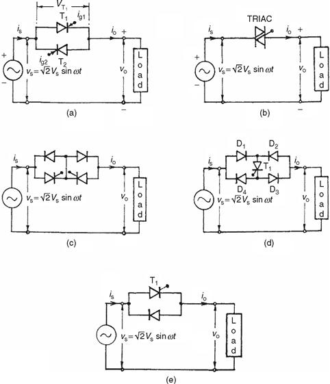
FIGURE 18.1 Single-phase ac voltage controllers: (a) fall wave, two SCRs in inverse-parallel; (b) fall wave with triac; (c) fall wave with two SCRs and two diodes; (d) full wave with four diodes and one SCR; and (e) half wave with one SCR and one diode in antiparallel.
With phase control, the switches conduct the load current for a chosen period of each input cycle of voltage and with on/off control, the switches connect the load either for a few cycles of input voltage and disconnect it for the next few cycles (integral cycle control) or the switches are turned on and off several times within alternate half cycles of input voltage (ac chopper or pulse width modulated [PWM] ac voltage controller).
18.2.1 Phase-Controlled Single-phase AC Voltage Controller
For a full-wave symmetrical phase control, the SCRs T1 and T2 in Fig. 18.1a are gated at α and π+α, respectively, from the zero crossing of the input voltage; by varying α, the power flow to the load is controlled through voltage control in alternate half cycles. As long as one SCR is carrying current, the other SCR remains reverse-biased by the voltage drop across the conducting SCR. The principle of operation in each half cycle is similar to that of the controlled half-wave rectifier, and one can use the same approach for analysis of the circuit.
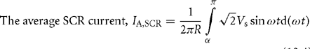
Operation with R-load: Figure 18.2 shows the typical voltage and current waveforms for the single-phase bidirectional phase-controlled ac voltage controller of Fig. 18.1a with a resistive load. The output voltage and current waveforms have half-wave symmetry and so no dc component.
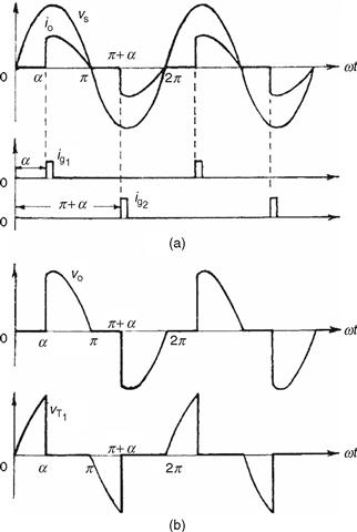
FIGURE 18.2 Waveforms for single-phase ac fall-wave voltage controller with R-load.
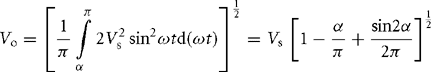
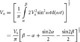
If ![]() sin ωt is the source voltage, the rms output voltage with T1 triggered at α can be found from the half-wave symmetry as
sin ωt is the source voltage, the rms output voltage with T1 triggered at α can be found from the half-wave symmetry as
 (18.1)
Note that Vo can be varied from Vs to 0 by varying α from 0 to π.
![]() (18.2)
(18.2)
 (18.3)
 (18.4)
Since each SCR carries half the line current, the rms current in each SCR is
![]() (18.5)
(18.5)
Operation with RL Load: Figure 18.3 shows the voltage and current waveforms for the controller in Fig. 18.1a with RL load. Due to the inductance, the current carried by the SCR T1 may not fall to zero at ωt = π when the input voltage goes negative and may continue till ωt = β, the extinction angle, as shown. The conduction angle,
![]() (18.6)
(18.6)
of the SCR depends on the firing delay angle α and the load impedance angle ϕ.
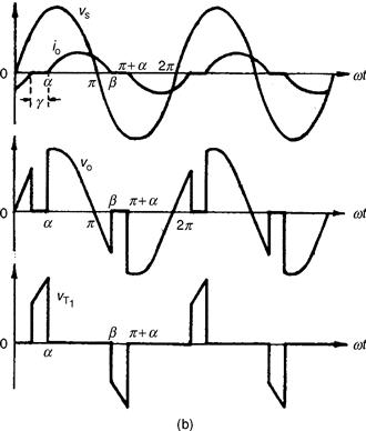
FIGURE 18.3 Typical waveforms of single-phase ac voltage controller with an RL load.
The expression for the load current Io (ωt), when conducting from α to ß, can be derived in the same way as that used for a phase-controlled rectifier in a discontinuous mode by solving the relevant Kirchoff's voltage equation:
 (18.7)
where Z = (R2 + ω2 L2)½ = load impedance and ϕ = load impedance angle = tan− 1 (ωL/R).
The angle β, when the current io falls to zero, can be determined from the following transcendental equation resulted by using io (ωt = β) = 0 in Eq. (18.7).
![]() (18.8)
(18.8)
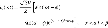
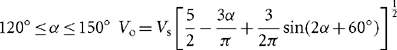
From Eqs. (18.6) and (18.8), one can obtain a relationship between θ and α for a given value of ϕ, as shown in Fig. 18.4, which shows that as α is increased, the conduction angle θ decreases, and thus the rms value of the current decreases.
FIGURE 18.4 θ versus α curves for single-phase ac voltage controller with RL load.
The rms output voltage
 (18.9)
Vo can be evaluated for two possible extreme values of ϕ = 0 when β = π, and ϕ = π/2 when β = 2π –α, and the envelope of the voltage control characteristics for this controller is shown in Fig. 18.5.
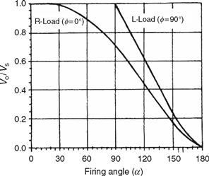
FIGURE 18.5 Envelope of control characteristics of a single-phase ac voltage controller with RL load.
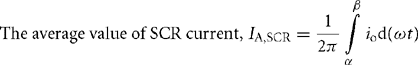
The rms SCR current can be obtained from Eq. (18.7) as follows:
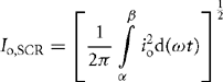 (18.10)
![]() (18.11)
(18.11)
 (18.12)
Gating Signal Requirements: For the inverse-parallel SCRs as shown in Fig. 18.1a, the gating signals of SCRs must be isolated from one another because there is no common cathode. For R-load, each SCR stops conducting at the end of each half cycle and under this condition, single short pulses may be used for gating as shown in Fig. 18.2. With RL load, however, this single short pulse gating is not suitable as shown in Fig. 18.6. When SCR T2 is triggered at ωt = π + α, SCR T1 is still conducting due to the load inductance. By the time the SCR T1 stops conducting at β, the gate pulse for SCR T2 has already ceased and T2 will fail to turn on resulting the converter to operate as a single-phase rectifier with conduction of T1 only. This necessitates the application of a sustained gate pulse either in the form of a continuous signal for the half-cycle period, which increases the dissipation in SCR gate circuit and a large isolating pulse transformer or better a train of pulses (carrier frequency gating) to overcome these difficulties.
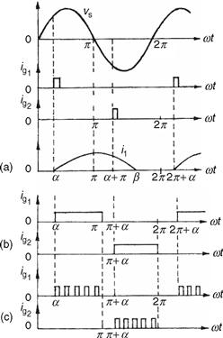
FIGURE 18.6 Single-phase fall-wave controller with RL load: gate pulse requirements.
Operation with α<ϕ If α = ϕ, then from Eq. (18.8),
![]() (18.13)
(18.13)
![]() (18.14)
(18.14)
As the conduction angle θ cannot exceed π and the load current must pass through zero, the control range of the firing angle is ϕ ≤ α ≤ π. With narrow gating pulses and α < ϕ, only one SCR will conduct resulting in a rectifier action as shown. Even with a train of pulses, if α < ϕ, the changes in the firing angle will not change the output voltage and current but both the SCRs will conduct for the period π with T1 becoming on at ωt = π and T2 at ωt + π.
The duration of this dead zone (α = 0 to ϕ), which varies with the load impedance angle ϕ is not a desirable feature in closed-loop control schemes. An alternative approach to the phase control with respect to the input voltage zero crossing has been visualized in which the firing angle is defined with respect to the instant when it is the load current, not the input voltage, that reaches zero, this angle being called the hold-off angle (γ) or the control angle (as marked in Fig. 18.3). This method needs sensing the load current, which may otherwise be required in a closed-loop controller for monitoring or control purposes.
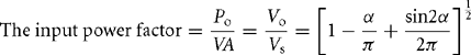
Power Factor and Harmonics: As in the case of phase-controlled rectifiers, the important limitations of the phase-controlled ac voltage controllers are the poor power factor and the introduction of harmonics in the source currents. As seen from Eq. (18.3), the input power factor depends on α and as α increases, the power factor decreases.
The harmonic distortion increases and the quality of the input current decreases with increase of firing angle. The variations of low-order harmonics with the firing angle as computed by Fourier analysis of the voltage waveform of Fig. 18.2 (with R-load) are shown in Fig. 18.7. Only odd harmonics exist in the input current because of half-wave symmetry.
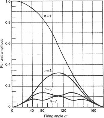
FIGURE 18.7 Harmonic content as a function of the firing angle for a single-phase voltage controller with RL load.
18.2.2 Single-Phase AC–AC Voltage Controller with On/Off Control
Integral Cycle Control: As an alternative to the phase control, the method of integral cycle control or burst-firing is used for heating loads. Here, the switch is turned on for a time tn with n integral cycles and turned off for a time tm with m integral cycles (Fig. 18.8). As the SCRs or triacs used here are turned on at the zero crossing of the input voltage and turn off occurs at zero current, supply harmonics and radio frequency interference are very low.
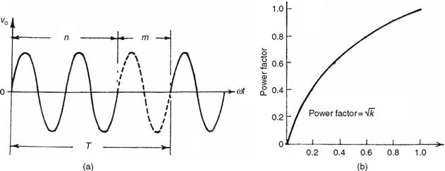
FIGURE 18.8 Integral cycle control: (a) typical load voltage waveforms and (b) power factor with the duty cycle k.
However, subharmonic frequency components maybe generated, which are undesirable because they may set up sub-harmonic resonance in the power supply system, cause lamp flicker, and may interfere with the natural frequencies of motor loads causing shaft oscillations.
For sinusoidal input voltage, ![]() sin ωt, the rms output voltage,
sin ωt, the rms output voltage,
![]() (18.15)
(18.15)
and Vs = rms phase voltage
![]() (18.16)
(18.16)
which is poorer for lower values of the duty cycle k.
PWM AC Chopper: As in the case of controlled rectifier, the performance of ac voltage controllers can be improved in terms of harmonics, quality of output current, and input power factor by PWM control in PWM ac choppers; the circuit configuration of one such single-phase unit is shown in Fig. 18.9. Here, fully controlled switches S1 and S2 connected in anti-parallel are turned on and off many times during the positive and negative half cycles of the input voltage, respectively. S’1 and S’2 provide the freewheeling paths for the load current when S1 and S2 are off. An input capacitor filter may be provided to attenuate the high switching frequency currents drawn from the supply and also to improve the input power factor. Figure 18.10 shows the typical output voltage and load current waveform for a single-phase PWM ac chopper. It can be shown that the control characteristics of an ac chopper depend on the modulation index M, which theoretically varies from 0 to 1.
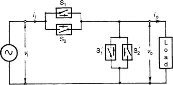
FIGURE 18.9 Single-phase PWM ac chopper circuit.
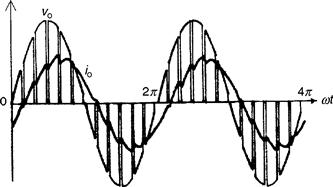
FIGURE 18.10 Typical output voltage and current waveforms of a single-phase PWM ac chopper.
Three-phase PWM choppers consist of three single-phase choppers either connected in delta or four-wire (star) configuration.
18.3 Three-Phase AC–AC Voltage Controllers
18.3.1 Phase-Controlled Three-Phase AC Voltage Controllers
Various Configurations: Several possible circuit configurations for three-phase phase-controlled ac regulators with star or delta connected loads are shown in Fig. 18.11a–h.
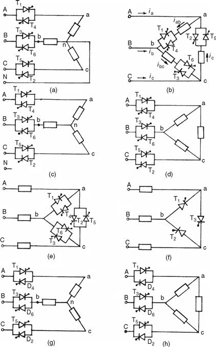
FIGURE 18.11 Three-phase ac voltage controller circuit configurations.
The configurations in (a) and (b) can be realized by three single-phase ac regulators operating independently of each other, and they are easy to analyze. In (a), the SCRs are to be rated to carry line currents and withstand phase voltages, whereas in (b) they should be capable to carry phase currents and withstand the line voltage. In (b), the line currents are free from triplen harmonics while these are present in the closed delta. The power factor in (b) is slightly higher. The firing angle control range for both these circuits is 0–180° for R-load.
The circuits in (c) and (d) are three-phase three-wire circuits and are complicated to analyze. In both these circuits, at least two SCRs, one in each phase, must be gated simultaneously to get the controller started by establishing a current path between the supply lines. This necessitates two firing pulses spaced at 60° apart per cycle for firing each SCR. The operation modes are defined by the number of SCRs conducting in these modes. The firing control range is 0–150°. The triplen harmonics are absent in both these configurations.
Another configuration is shown in (e) when the controllers are connected in delta and the load is connected between the supply and the converter. Here, current can flow between two lines even if one SCR is conducting so each SCR requires one firing pulse per cycle. The voltage and current ratings of SCRs are nearly the same as that of the circuit (b). It is also possible to reduce the number of devices to three SCRs in delta as shown in (f), connecting one source terminal directly to one load circuit terminal. Each SCR is provided with gate pulses in each cycle spaced at 120° apart. In both (e) and (f), each end of each phase must be accessible. The number of devices in (f) is less, but their current ratings must be higher.
As in the case of single-phase phase-controlled voltage regulator, the total regulator cost can be reduced by replacing six SCRs by three SCRs and three diodes, resulting in three-phase half-wave controlled unidirectional ac regulators as shown in (g) and (h) for star- and delta-connected loads. The main drawback of these circuits is the large harmonic content in the output voltage –particularly, the second harmonic because of the asymmetry. However, the dc components are absent in the line. The maximum firing angle in the half-wave controlled regulator is 210°.
18.3.2 Fully Controlled Three-Phase Three-Wire AC Voltage Controller
Star-connected Load with Isolated Neutral: The analysis of operation of the full-wave controller with isolated neutral as shown in Fig. 18.11c is, as mentioned, quite complicated in comparison to that of a single-phase controller, particularly for an RL or motor load. As a simple example, the operation of this controller with a simple star-connected R-load is considered here. The six SCRs are turned on in the sequence 1-2-3-4-5-6 at 60° intervals, and the gate signals are sustained throughout the possible conduction angle.
The output phase voltage waveforms for α = 30°, 75°, and 120° for a balanced three-phase R-load are shown in Fig. 18.12. At any interval, either three SCRs, or two SCRs, or no SCRs may be on, and the instantaneous output voltages to the load are either a line-to-neutral voltage (three SCRs on), or one-half of the line-to-line voltage (two SCRs on), or zero (no SCR on).
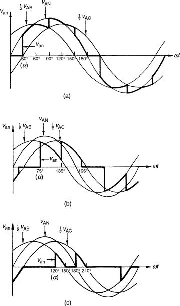
FIGURE 18.12 Output voltage waveforms for a three-phase ac voltage controller with star-connected R-load: (a) van for α = 30°; (b) van for α = 75°; and (c) van = 120°.
Depending on the firing angle α, there may be three operating modes:
Mode I (also known as Mode 2/3): 0 ≤ α ≤ 60°; There are periods when three SCRs are conducting, one in each phase for either direction, and there are periods when just two SCRs conduct.
For example, with α = 30° in Fig. 18.12a, assume that at ωt = 0, SCRs ?5 and T6 are conducting, and the current through the R-load in a-phase is zero making van = 0. At ωt = 30°, T1 receives a gate pulse and starts conducting; T5 and T6 remain on and van = vAN. The current in T5 reaches zero at 60°, turning T5 off. With T1 and T6 staying on, vAN = ½vAB. At 90°, T2 is turned on, the three SCRs T1, T2, and T6 are then conducting and van = van. At 120°, T6 turns off, leaving T1 and T2 on, so van = ½vac. Thus with the progress of firing in sequence till α = 60°, the number of SCRs conducting at a particular instant alternates between two and three.
Mode II (also known as Mode 2/2): 60° ≤ α ≤ 90°; Two SCRs, one in each phase, always conduct.
For α = 75° as shown in Fig. 18.12b, just prior to α = 75°, SCRs T5 and T6 were conducting and van = 0. At 75°, T1 is turned on, and T6 continues to conduct, whereas T5 turns off as vCN is negative. vAN = ½vαβ. When T2 is turned on at 135°, T6 is turned off and vAN = ½vAC. The next SCR to turn on is T3, which turns off T1 and vAN = 0. One SCR is always turned off when another is turned on in this range of α, and the output voltage is either one-half line-to-line voltage or zero.
Mode III (also known as Mode 0/2): 90° ≤ α ≤ 150°; When none or two SCRs conduct.
For α = 120°, Fig. 18.12c, earlier no SCRs were on and van = 0. At α = 120°, SCR T1 is given a gate signal, whereas T6 has a gate signal already applied. Since vAB is positive, T1 and T6 are forward-biased and they begin to conduct and vAN = ½vAB. Both T1 and T6 turn off when vAB becomes negative. When a gate signal is given to T2, it turns on and T1 turns on again.
For α 150°, there is no period when two SCRs are conducting and the output voltage is zero at α = 150°. Thus, the range of the firing angle control is 0 ≤ α ≤ 150°.
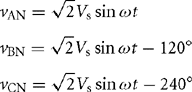
For star-connected R-load, assuming the instantaneous phase voltages as
 (18.17)
the expressions for the rms output phase voltage Vo can be derived for the three modes as follows:
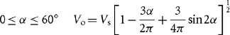 (18.18)
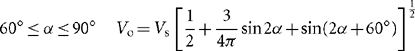 (18.19)
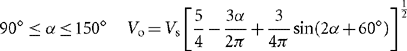 (18.20)
For star-connected pure L-load, the effective control starts at α > 90°, and the expressions for two ranges of a are as follows:
 (18.21)
 (18.22)
The control characteristics for these two limiting cases (ϕ = 0 for R-load and ϕ = 90° for L-load) are shown in Fig. 18.13. Here also, like the single-phase case, the dead zone may be avoided by controlling the voltage with respect to the control angle or hold-off angle (y) from the zero crossing of current in place of the firing angle α.
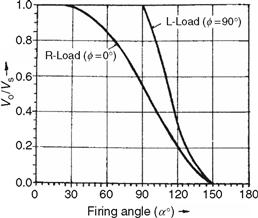
FIGURE 18.13 Envelope of control characteristics for a three-phase full-wave ac voltage controller.
RL Load: The analysis of the three-phase voltage controller with star-connected RL load with isolated neutral is quite complicated, since the SCRs do not cease to conduct at voltage zero, and the extinction angle β is to be known by solving the transcendental equation for the case. In this case, the Mode II operation disappears [1], and the operation shift from Mode I to Mode III depends on the so-called critical angle αcrit [2, 3], which can be evaluated from a numerical solution of the relevant transcendental equations. Computer simulation either by PSPICE program [4, 5] or a switching-variable approach coupled with an iterative procedure [6] is a practical means of obtaining the output voltage waveform in this case. Figure 18.14 shows typical simulation results using the later approach [6] for a three-phase voltage controller fed RL load for α = 60°, 90°, and 105°, which agree with the corresponding practical oscillograms given in [7].
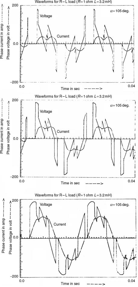
FIGURE 18.14 Typical simulation results for three-phase ac voltage controller-fed RL load (R = 1Ω, L = 3.2 mH) for α = 60°, 90°, and 105°.
Delta-Connected R-Load: The configuration is shown in Fig. 18.11b. The voltage across an R-load is the corresponding line-to-line voltage when one SCR in that phase is on. Figure 18.15 shows the line and phase currents for α = 130° and 90° with an R-load. The firing angle α is measured from the zero crossing of the line-to-line voltage, and the SCRs are turned on in the sequence as they are numbered. As in the single-phase case, the range of firing angle is 0 ≤ α ≤ 180°. The line currents can be obtained from the phase currents as follows:
 (18.23)
FIGURE 18.15 Waveforms of a three-phase ac voltage controller with a delta connected R-load: (a) α = 120° and (b) α = 90°.
The line currents depend on the firing angle and may be discontinuous as shown. Due to the delta connection, the triplen harmonic currents flow around the closed delta and do not appear in the line. The rms value of the line current varies between the range
![]() (18.24)
(18.24)
as the conduction angle varies from very small (largea) to 180° (α = 0).
18.4 Cycloconverters
In contrast to the ac voltage controllers operating at constant frequency, discussed so far, a cycloconverter operates as a direct ac–ac frequency changer with inherent voltage control feature. The basic principle of this converter to construct an alternating voltage wave of lower frequency from successive segment of voltage waves of higher frequency ac supply by a switching arrangement was conceived and patented in 1920s. Grid-controlled mercury-arc rectifiers were used in these converters installed in Germany in 1930s to obtain 16![]() -Hz single-phase supply for ac series traction motors from a three-phase 50-Hz system, while at the same time a cycloconverter using 18 thyratrons supplying a 400 hp synchronous motor was in operation for some years as a power station auxiliary drive in the United States. However, the practical and commercial utilization of these schemes waited till the SCRs became available in 1960s. With the development of large-power SCRs and micropocessor-based control, the cycloconverter today is a matured practical converter for application in large-power low-speed variable-voltage variable-frequency (VVVF) ac drives in cement and steel rolling mills, as well as in variable-speed constant-frequency (VSCF) systems in air crafts and naval ships.
-Hz single-phase supply for ac series traction motors from a three-phase 50-Hz system, while at the same time a cycloconverter using 18 thyratrons supplying a 400 hp synchronous motor was in operation for some years as a power station auxiliary drive in the United States. However, the practical and commercial utilization of these schemes waited till the SCRs became available in 1960s. With the development of large-power SCRs and micropocessor-based control, the cycloconverter today is a matured practical converter for application in large-power low-speed variable-voltage variable-frequency (VVVF) ac drives in cement and steel rolling mills, as well as in variable-speed constant-frequency (VSCF) systems in air crafts and naval ships.
A cycloconverter is a naturally commuted converter with inherent capability of bidirectional power flow, and there is no real limitation on its size unlike an SCR inverter with commutation elements. Here, the switching losses are considerably low, the regenerative operation at full power over complete speed range is inherent and it delivers a nearly sinusoidal waveform resulting in minimum torque pulsation and harmonic heating effects. It is capable of operating even with blowing out of individual SCR fuse (unlike inverter), and the requirements regarding turn-off time, current rise time, and dv/dt sensitivity of SCRs are low. The main limitations of a naturally commutated cycloconverter are (1) limited frequency range for subharmonic free and efficient operation and (2) poor input displacement/power factor, particularly at low-output voltages.
18.4.1 Single-Phase to Single-Phase Cycloconverter
Though rarely used, the operation of a single-phase to single-phase cycloconverter is useful to demonstrate the basic principle involved. Figure 18.16a shows the power circuit of a single-phase bridge type of cycloconverter, which has the same arrangement as that of a single-phase dual converter. The firing angles of the individual two-pulse two-quadrant bridge converters are continuously modulated here, so that each ideally produces the same fundamental ac voltage at its output terminals as marked in the simplified equivalent circuit in Fig. 18.16b. Because of the unidirectional current carrying property of the individual converters, it is inherent that the positive half cycle of the current is carried by the P-converter and the negative half cycle of the current by the N-converter regardless of the phase of the current with respect to the voltage. This means that for a reactive load, each converter operates in both rectifying and inverting region during the period of the associated half cycle of the low-frequency output current.
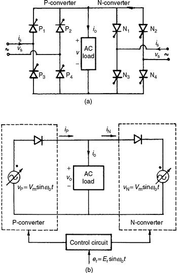
FIGURE 18.16 (a) Power circuit for a single-phase bridge cycloconverter and (b) simplified equivalent circuit of a cycloconverter.
Operation with R-Load: Figure 18.17 shows the input and output voltage waveforms with a pure R-load for a 50–16![]() -Hz cycloconverter. The P- and N-converters operate for alternate To/2 periods. The output frequency (1/To) can be varied by varying To and the voltage magnitude by varying the firing angle α of the SCRs. As shown in the figure, three cycles of the ac input wave are combined to produce one cycle of the output frequency to reduce the supply frequency to one-third across the load.
-Hz cycloconverter. The P- and N-converters operate for alternate To/2 periods. The output frequency (1/To) can be varied by varying To and the voltage magnitude by varying the firing angle α of the SCRs. As shown in the figure, three cycles of the ac input wave are combined to produce one cycle of the output frequency to reduce the supply frequency to one-third across the load.
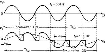
FIGURE 18.17 Input and output waveforms of a 50–16![]() -Hz cycloconverter with RL load.
-Hz cycloconverter with RL load.
If αp is the firing angle of the P-converter, the firing angle of the N-converter αN is π –αP and the average voltage of the P-converter is equal and opposite to that of the N-converter.
The inspection of Fig. 18.17 shows that the waveform with α remaining fixed in each half cycle generates a square wave having a large low-order harmonic content. A near approximation to sine wave can be synthesized by a phase modulation of the firing angles as shown in Fig. 18.18 for a 50–10-Hz cycloconverter. The harmonics in the load voltage waveform are less compared to earlier waveform. The supply current, however, contains a subharmonic at the output frequency for this case as shown.
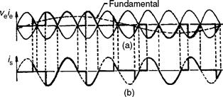
FIGURE 18.18 Waveforms of a single-phase single-phase cycloconverter (50–10 Hz) with RL load: (a) load voltage and load current and (b) input supply current.
Operation with RL Load: The cycloconverter is capable of supplying loads of any power factor. Figure 18.19 shows the idealized output voltage and current waveforms for a lagging power factor load where both the converters are operating as rectifier and inverter at the intervals marked. The load current lags the output voltage and the load current direction determines which converter is conducting. Each converter continues to conduct after its output voltage changes polarity and during this period, the converter acts as an inverter and the power is returned to the ac source. Inverter operation continues till the other converter starts to conduct. By controlling the frequency of oscillation and the depth of modulation of the firing angles of the converters (as shown later), it is possible to control the frequency and the amplitude of the output voltage.
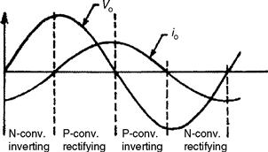
FIGURE 18.19 Idealized load voltage and current waveform for a cycloconverter with RL load.
The load current with RL load may be continuous or discontinuous depending on the load phase angle, ϕ. At light load inductance or for ϕ ≤ α ≤ π, there may be discontinuous load current with short zero-voltage periods. The current wave may contain even harmonics and subharmonic components. Further, as in the case of dual converter, although the mean output voltage of the two converters is equal and opposite, the instantaneous values may be unequal and a circulating current can flow within the converters. This circulating current can be limited by having a center-tapped reactor connected between the converters or can be completely eliminated by logical control similar to the dual converter case when the gate pulses to the converter remaining idle are suppressed, when the other converter is active. In practice, a zero-current interval of short duration is needed, in addition, between the operation of the P- and N-converters to ensure that the supply lines of the two converters are not short-circuited. With circulating current-free operation, the control scheme becomes complicated if the load current is discontinuous.
In the case of the circulating current scheme, the converters are kept in virtually continuous conduction over the whole range, and the control circuit is simple. To obtain reasonably good sinusoidal voltage waveform using the line-commutated two quadrant converters and eliminate the possibility of the short circuit of the supply voltages, the output frequency of the cycloconverter is limited to a much lower value of the supply frequency. The output voltage waveform and the output frequency range can be improved further by using converters of higher pulse numbers.
18.4.2 Three-Phase Cycloconverters
18.4.2.1 Three-Phase Three-Pulse Cycloconverter
Figure 18.20a shows the schematic diagram of a three-phase half-wave (three-pulse) cycloconverter feeding a single-phase load and Fig. 18.20b, the configuration of a three-phase half-wave (three-pulse) cycloconverter feeding a three-phase load.
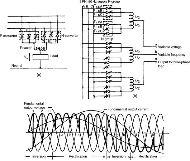
FIGURE 18.20 (a) Three-phase half-wave (three-pulse) cycloconverter supplying a single-phase load; (b) three-pulse cycloconverter supplying a three-phase load; and (c) output voltage waveform for one phase of a three-pulse cycloconverter operating at 15 Hz from a 50-Hz supply and 0.6-power factor lagging load.
The basic process of a three-phase cycloconversion is illustrated in Fig. 18.20c at 15 Hz, 0.6-power factor lagging load from a 50-Hz supply. As the firing angle α is cycled from zero at “a” to 180° at “j,” half a cycle of output frequency is produced (the gating circuit is to be suitably designed to introduce this oscillation of the firing angle). For this load, it can be seen that although the mean output voltage reverses at X, the mean output current (assumed sinusoidal) remains positive until Y. During XY, the SCRs A, B, and C in P-converter are “inverting.”
A similar period exists at the end of the negative half cycle of the output voltage when D, E, and F SCRs in N-converter are “inverting.” Thus, the operation of the converter follows in the order of “rectification” and “inversion” in a cyclic manner, the relative durations are dependent on load power factor. The output frequency is that of the firing angle oscillation about a quiescent point of 90° (condition when the mean output voltage, given by Vo = Vdo cos α, is zero). For obtaining the positive half cycle of the voltage, firing angle α is varied from 90° to 0° and then to 90° and for the negative half cycle, from 90° to 180° and back to 90°. Variation of α within the limits of 180° automatically provides for “natural” line commutation of the SCRs. It is shown that a complete cycle of low-frequency output voltage is fabricated from the segments of the three-phase input voltage by using the phase-controlled converters. The P-converter or N-converter SCRs receive firing pulses, which are timed such that each converter delivers the same mean output voltage. This is achieved, as in the case of single-phase cycloconverter or the dual converter, by maintaining the firing angle constraints of the two groups as αp = 180° –αN. However, the instantaneous voltages of two converters are not identical and large circulating current may result unless limited by inter-group reactor as shown (circulating-current cycloconverter) or completely suppressed by removing the gate pulses from the non-conducting converter by an intergroup blanking logic (circulating-current-free cycloconverter).
Circulating-Current Mode Operation: Figure 18.21 shows typical waveforms of a three-pulse cycloconverter operating with circulating current. Each converter conducts continuously with rectifying and inverting modes as shown, and the load is supplied with an average voltage of two converters reducing some of the ripple in the process, the intergroup reactor behaving as a potential divider. The reactor limits the circulating current; the value of its inductance to the flow of load current is one-fourth of its value to the flow of circulating current as the inductance is proportional to the square of the number of turns. The fundamental wave produced by both the converters is the same. The reactor voltage is the instantaneous difference between the converter voltages, and the time integral of this voltage divided by the inductance (assuming negligible circuit resistance) is the circulating current. For a three-pulse cycloconverter, it can be observed that this current reaches its peak when αP = 60° and αN = 120°.
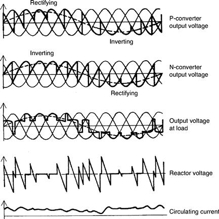
FIGURE 18.21 Waveforms of a three-pulse cycloconverter with circulating current.
Output Voltage Equation: A simple expression for the fundamental rms output voltage of the cycloconverter and the required variation of the firing angle α can be derived with the following assumptions: (1) the firing angle α in successive half cycles is varied slowly resulting in a low-frequency output; (2) the source impedance and the commutation overlap are neglected; (3) the SCRs are ideal switches; and (4) the current is continuous and ripple-free. The average dc output voltage of a p-pulse dual converter with fixed α is
![]() (18.25)
(18.25)
For the p-pulse dual converter operating as a cycloconverter, the average phase voltage output at any point of the low frequency should vary according to the equation
![]() (18.26)
(18.26)
where Vo1,max is the desired maximum value of the fundamental output of the cycloconverter.
Comparing Eq. (18.25) with Eq. (18.26), the required variation of a to obtain α sinusoidal output is given by
![]() (18.27)
(18.27)
where r is the ratio (Vo1,max/Vdomax), the voltage magnitude control ratio.
Equation (18.27) shows a as a nonlinear function with r (≤ 1) as shown in Fig. 18.22.
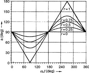
FIGURE 18.22 Variations of the firing angle (α) with r in a cycloconverter.
However, the firing angle αp of the P-converter cannot be reduced to 0° as this corresponds to αN = 180° for the N-converter which, in practice, cannot be achieved because of allowance for commutation overlap and finite turn-off time of the SCRs. Thus, the firing angle αP can be reduced to a certain finite value αmin, and the maximum output voltage is reduced by a factor cos αmin.
The fundamental rms voltage per phase of either converter is
![]() (18.28)
(18.28)
Though the rms values of the low-frequency output voltage of the P-converter and that of the N-converter are equal, the actual waveforms differ and the output voltage at the midpoint of the circulating current-limiting reactor (Fig. 18.21), which is the same as the load voltage, is obtained as the mean of the instantaneous output voltages of the two converters.
Circulating Current-free Mode Operation: Figure 18.23 shows the typical waveforms for a three-pulse cycloconverter operating in this mode with RL load assuming continuous-current operation. Depending on the load current direction, only one converter operates at a time and the load voltage is the same as the output voltage of the conducting converter. As explained earlier in the case of single-phase cycloconverter, there is a possibility of short circuit of the supply voltages at the cross-over points of the converter unless taken care of in the control circuit. The waveforms drawn also neglect the effect of overlap due to the ac supply inductance. A reduction in the output voltage is possible by retarding the firing angle gradually at the points a, b, c, d, e in Fig. 18.23. (This can be easily implemented by reducing the magnitude of the reference voltage in the control circuit). The circulating current is completely suppressed by blocking all the SCRs in the converter, which is not delivering the load current. A current sensor is incorporated in each output phase of the cycloconverter, which detects the direction of the output current and feeds an appropriate signal to the control circuit to inhibit or blank the gating pulses to the nonconducting converter in the same way as in the case of a dual converter for dc drives. The circulating current-free operation improves the efficiency, and the displacement factor of the cycloconverter and also increases the maximum usable output frequency. The load voltage transfers smoothly from one converter to the other.
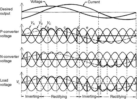
FIGURE 18.23 Waveforms for a three-pulse circulating current-free cycloconverter with RL load.
18.4.2.2 Three-Phase Six-Pulse and Twelve-Pulse Cycloconverter
A six-pulse cycloconverter circuit configuration is shown in Fig. 18.24. Typical load voltage waveforms for 6-pulse (with 36 SCRs) and 12-pulse (with 72 SCRs) cycloconverters are shown in Fig. 18.25, the 12-pulse converter being obtained by connecting two 6-pulse configurations in series and appropriate transformer connections for the required phase-shift. It may be seen that the higher pulse numbers will generate waveforms closer to the desired sinusoidal form and thus permit higher frequency output. The phase loads maybe isolated from each other as shown or interconnected with suitable secondary winding connections.
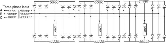
FIGURE 18.24 Three-phase six-pulse cycloconverter with isolated loads.
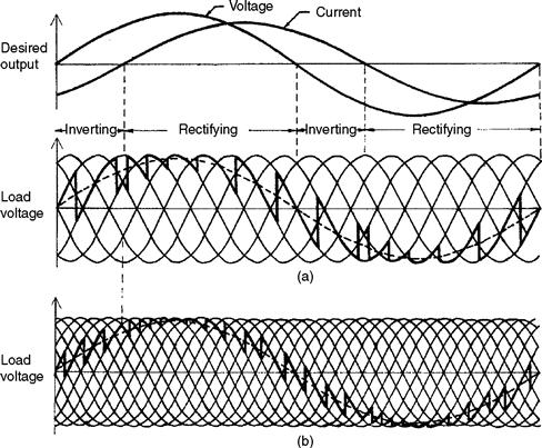
FIGURE 18.25 Cycloconverter load voltage waveforms with lagging power factor load: (a) six-pulse connection and (b) twelve-pulse connection.
18.4.3 Cycloconverter Control Scheme
Various possible control schemes, analog as well as digital, for deriving trigger signals and for controlling the basic cycloconverter have been developed over the years.
Out of the several possible signal combinations, it has been shown [8] that a sinusoidal reference signal (er = Er sin ω t) at desired output frequency fo and a cosine modulating signal (em = Em cos ωi t) at input frequency fi is the best combination possible for comparison to derive the trigger signals for the SCRs (Fig. 18.26 [9]), which produces the output waveform with the lowest total harmonic distortion. The modulating voltages can be obtained as the phase-shifted voltages (B-phase for A-phase SCRs, C-phase voltage for B-phase SCRs, and so on) as explained in Fig. 18.27, where at the intersection point “a”
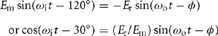
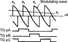
FIGURE 18.26 Deriving firing signals for one converter group of a three-pulse cycloconverter.
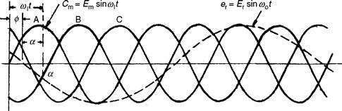
FIGURE 18.27 Derivation of the cosine modulating voltages.
From Fig. 18.27, the firing delay for A-phase SCR, α = (ωi t – 30°)
![]()
The cycloconverter output voltage for continuous current operation,
![]() (18.29)
(18.29)
in which the equation shows that the amplitude, frequency, and phase of the output voltage can be controlled by controlling corresponding parameters of the reference voltage, thus making the transfer characteristic of the cycloconverter linear. The derivation of the two complimentary voltage waveforms for the P-group or N-group converter “banks” in this way is illustrated in Fig. 18.28. The final cycloconverter output wave shape is composed of alternate half cycle segments of the complementary P-converter and the N-converter output voltage wave forms which coincide with the positive and negative current half cycles, respectively.
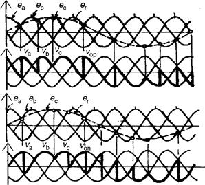
FIGURE 18.28 Derivation of P-converter and N-converter output voltages.
Control Circuit Block Diagram: Figure 18.29 [10] shows a simplified block diagram of the control circuit for a circulating current-free cycloconverter implemented with ICs in the early seventies in the Power Electronics Laboratory at IIT Kharagpur in India. The same circuit is also applicable to a circulating current cycloconverter with the omission of the converter group selection and blanking circuit.
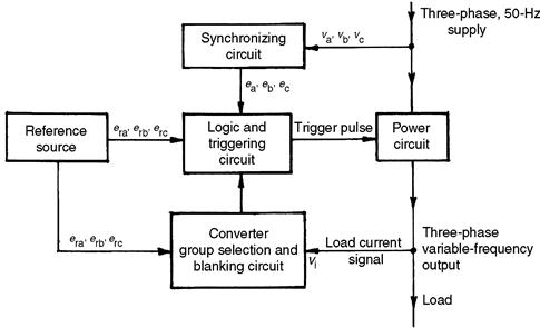
FIGURE 18.29 Block diagram for a circulating current-free cycloconverter control circuit.
The synchronizing circuit produces the modulating voltages (ea = –Kvb, eb = –Kvc, ec = –Kva), synchronized with the mains through step-down transformers and proper filter circuits.
The reference source produces variable voltage variable frequency reference signal (era, erb, erc) (three-phase for a three-phase cycloconverter) for comparison with the modulation voltages. Various ways, analog or digital, have been developed to implement this reference source as in the case of the PWM inverter. In one of the early analog schemes Fig. 18.30 [10], for a three-pulse cycloconverter, a variable-frequency UJT relaxation oscillator of frequency 6fd triggers a ring counter to produce a three-phase square-wave output of frequency fd which is used to modulate a single-phase fixed frequency (fc) variable amplitude sinusoidal voltage in a three-phase full-wave transistor chopper. The three-phase output contains (fc –fd), (fc + fd), (3fd + fc), etc. frequency components from where the “wanted” frequency component (fc –fd) is filtered out for each phase using a low-pass filter. For example, with fc = 500 Hz and frequency of the relaxation oscillator varying between 2820 and 3180 Hz, a three phase 0–30-Hz reference output can be obtained with the facility for phase sequence reversal.
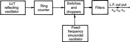
FIGURE 18.30 Block diagram of a variable-voltage variable-frequency three-phase reference source.
The logic and trigger circuit for each phase involves comparators for comparison of the reference and modulating voltages, and inverters acting as buffer stages. The outputs of the comparators are used to clock the flip-flops or latches whose outputs in turn feed the SCR gates through AND gates and pulse amplifying and isolation circuits; the second input to the AND gates is from the converter group selection and blanking circuit.
In the converter group selection and blanking circuit, the zero crossing of the current at the end of each half cycle is detected and is used to regulate the control signals either to P-group or N-group converters depending on whether the current goes to zero from negative to positive or positive to negative, respectively. However, in practice, the current being discontinuous passes through multiple zero crossings while changing direction, which may lead to undesirable switching of the converters. So, in addition to the current signal, the reference voltage signal is also used for the group selection, and a threshold band is introduced in the current signal detection to avoid inadvertent switching of the converters. Further, a delay circuit provides a blanking period of appropriate duration between the converter groups switching to avoid line-to-line short circuits [10]. In some schemes, the delays are not introduced when a small circulating current is allowed during cross-over instants limited by reactors of limited size, and this scheme operates in the so-called “dual mode” –circulating current and circulating current-free mode for minor and major portions of the output cycle, respectively. A different approach to the converter group selection, based on the closed-loop control of the output voltage where a bias voltage is introduced between the voltage transfer characteristics of the converters to reduce circulating current, is discussed in [8].
Improved Control Schemes: With the development of microprocessors and PC-based systems, digital software control has taken over many tasks in modern cycloconverters, particularly in replacing the low-level reference waveform generation and analog signal comparison units. The reference waveforms can be easily generated in the computer, stored in the EPROMs and accessed under the control of a stored program and microprocessor clock oscillator. The analog signal voltages can be converted to digital signals by using analog-to-digital converters (ADCs). The waveform comparison can then be made with the comparison features of the microprocessor system. The addition of time delays and intergroup blanking can also be achieved with digital techniques and computer software. A modification of the cosine firing control using communication principles, such as regular sampling in preference to the natural sampling (discussed so far) of the reference waveform, yielding a stepped sine wave before comparison with the cosine wave [11] has been shown to reduce the presence of sub harmonics (discussed later) in the circulating current-cycloconverter and facilitate microprocessor-based implementation, as in the case of PWM inverter.
For a six-pulse noncirculating current cycloconverter-fed synchronous motor drive with a vector control scheme and a flux observer, a PC-based hybrid control scheme (a combination of analog and digital control) has been reported in [12]. Here, the functions such as comparison, group selection, blanking between the groups and triggering signal generation, filtering and phase conversion are left to the analog controller and digital controller that take care of more serious tasks such as voltage decoupling for current regulation, flux estimation using observer, speed, flux and field current regulators using PI-controllers, position and speed calculation leading to an improvement of sampling time and design accuracy.
18.4.4 Cycloconverter Harmonics and Input Current Waveform
The exact wave shape of the output voltage of the cycloconverter depends on (1) the pulse number of the converter; (2) the ratio of the output to input frequency (fo/fi ); (3) the relative level of the output voltage; (4) load displacement angle; (5) circulating current or circulating current-free operation; and (6) the method of control of the firing instants. The harmonic spectrum of a cycloconverter output voltage is different and more complex than that of a phase-controlled converter. It has been revealed [8] that because of the continuous “to-and-fro” phase modulation of the converter firing angles, the harmonic distortion components (known as necessary distortion terms) have frequencies which are sums and differences between multiples of output and input supply frequencies.
Circulating Current-Free Operation: A derived general expression for the output voltage of a cycloconverter with circulating current-free operation [8] shows the following spectrum of harmonic frequencies for the 3-pulse, 6-pulse, and 12-pulse cycloconverters employing cosine modulation technique:
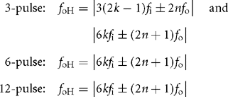 (18.30)
where k is any integer from 1 to infinity and n is any integer from 0 to infinity.
It may be observed that for certain ratios of fo/fi, the order of harmonics may be less or equal to the desired output frequency. All such harmonics are known as subharmonics, since they are not higher multiples of the input frequency. These subharmonics may have considerable amplitudes (e.g., with a 50-Hz input frequency and 35-Hz output frequency, a subharmonic of frequency 3 × 50 –4 × 35 = 10 Hz is produced whose magnitude is 12.5% of the 35-Hz component [11]) and are difficult to filter and so objectionable. Their spectrum increase with the increase of the ratio fo/fi and so limits its value at which a tolerable waveform can be generated.
Circulating-Current Operation: For circulating-current operation with continuous current, the harmonic spectrum in the output voltage is the same as that of the circulating current-free operation except that each harmonic family now terminates at a definite term, rather than having infinite number of components. They are
 (18.31)
The amplitude of each harmonic component is a function of the output voltage ratio for the circulating-current cycloconverter and the output voltage ratio as well as the load displacement angle for the circulating current-free mode.
From the point of view of maximum useful attainable output-to-input frequency ratio (fi/fo) with the minimum amplitude of objectionable harmonic components, a guideline is available in [8] for it as 0.33, 0.5, and 0.75 for 3-, 6-, and 12-pulse cycloconverter, respectively. However, with the modification of the cosine wave modulation timings like regular sampling [11] in the case of circulating-current cycloconverters only and using a subharmonic detection and feedback control concept [13, 14] for both circulating- and circulating-current-free cases, the subharmonics can be suppressed and useful frequency range for the naturally commutated cycloconverters can be increased.
Other Harmonic Distortion Terms: Besides the harmonics as mentioned, other harmonic distortion terms consisting of frequencies of integral multiples of desired output frequency appear, if the transfer characteristic between the output and reference voltages is not linear. These are called unnecessary distortion terms which are absent when the output frequencies are much less than the input frequency. Further, some practical distortion terms may appear due to some practical nonlinearities and imperfections in the control circuits of the cycloconverter, particularly at relatively lower levels of output voltage.
Input Current Waveform: Although the load current, particularly for higher pulse cycloconverters can be assumed to be sinusoidal, the input current is more complex being made of pulses. Assuming the cycloconverter to be an ideal switching circuit without losses, it can be shown from the instantaneous power balance equation that in cycloconverter supplying a single-phase load, the input current has harmonic components of frequencies (fI ± 2fo), called characteristic harmonic frequencies which are independent of pulse number and they result in an oscillatory power transmittal to the ac supply system. In the case of cycloconverter feeding a balanced three-phase load, the net instantaneous power is the sum of the three oscillating instantaneous powers when the resultant power is constant and the net harmonic component is much reduced compared to that of a single-phase load case. In general, the total rms value of the input current waveform consists of three components: in-phase, quadrature, and the harmonic. The in-phase component depends on the active power output while the quadrature component depends on the net average of the oscillatory firing angle and is always lagging.
18.4.5 Cycloconverter Input Displacement/Power Factor
The input supply performance of a cycloconverter such as displacement factor or fundamental power factor, input power factor, and the input current distortion factor are defined similar to those of the phase-controlled converter. The harmonic factor for the case of a cycloconverter is relatively complex as the harmonic frequencies are not simple multiples of the input frequency but are sums and differences between multiples of output and input frequencies.
Irrespective of the nature of the load, leading, lagging, or unity power factor, the cycloconverter requires reactive power decided by the average firing angle. At low output voltage, the average phase displacement between the input current and the voltage is large and the cycloconverter has a low input displacement and power factor. Besides load displacement factor and output voltage ratio, another component of the reactive current arises due to the modulation of the firing angle in the fabrication process of the output voltage [8]. In a phase-controlled converter supplying dc load, the maximum displacement factor is unity for maximum dc output voltage. However, in the case of the cycloconverter, the maximum input displacement factor is 0.843 with unity power factor load [8, 15]. The displacement factor decreases with reduction in the output voltage ratio. The distortion factor of the input current is given by (I1/I) which is always less than 1 and the resultant power factor (= distortion factor × displacement factor) is thus much lower (around 0.76 maximum) than the displacement factor and this is a serious disadvantage of the naturally commutated cycloconverter (NCC).
18.4.6 Effect of Source Impedance
The source inductance introduces commutation overlap and affects the external characteristics of a cycloconverter similar to the case of a phase-controlled converter with the dc output. It introduces delay in transfer of current from one SCR to another, results in a voltage loss at the output and a modified harmonic distortion. At the input, the source impedance causes “rounding off” of the steep edges of the input current waveforms, resulting in reduction in the amplitudes of higher order harmonic terms and a decrease in the input displacement factor.
18.4.7 Simulation Analysis of Cycloconverter Performance
The nonlinearity and discrete time nature of practical cycloconverter systems, particularly for discontinuous current conditions make an exact analysis quite complex and a valuable design and analytical tool is a digital computer simulation of the system. Two general methods of computer simulation of the cycloconverter waveforms for RL and induction motor loads with circulating current and circulating current-free operation have been suggested in [16] where one of the methods which is very fast and convenient is the cross-over points method that gives the cross-over points (intersections of the modulating and reference waveforms) and the conducting phase numbers for both P- and N-converters from which the output waveforms for a particular load can be digitally computed at any interval of time for a practical cycloconverter.
18.4.8 Power Quality Issues
Degradation of power quality (PQ) in a cycloconverter-fed system due to subharmonics/interharmonics in the input and the output has been a subject of recent studies [14, 17]. In [17], the study includes the impact of cycloconverter control strategies on the total harmonic distortion (THD), distribution transformers, and communication lines while in [14], the PQ indices are suitably defined and the effect on THD, input/output displacement factor and input/output power factor for a cycloconverter-fed synchronous motor drive are studied together with a development of a simple feedback method of reduction of subharmonics/low frequency interharmonics for improvement of the power quality. The implementation of this scheme, detailed in [14], requires a simple modification of the control circuit of the cycloconverter in contrast to the expensive power level active filters otherwise required for suppression of such harmonics [18].
18.4.9 Forced Commutated Cycloconverter
The naturally commutated cycloconverter (NCC) with SCRs as devices, so far discussed, is sometimes referred to as, a restricted frequency changer as in view of the allowance on the output voltage quality ratings, the maximum output voltage frequency is restricted (fo ![]() fi ), as mentioned earlier. With devices replaced by fully controlled switches like forced commutated SCRs, power transistors, IGBTs, GTOs, etc., a forced commutated cycloconverter can be built where the desired output frequency is given by fo = |fs –fi |, where fs is the switching frequency, which may be larger or smaller than the fi. In the case when fo ≥ fi, the converter is called unrestricted frequency changer (UFC) and when fo ≤ fi, it is called a slow switching frequency changer (SSFC). The early FCC structures have been comprehensively treated in [15]. It has been shown that in contrast with the NCC, when the input displacement factor (IDF) is always lagging, in UFC it is leading when the load displacement factor is lagging and vice versa, and in SSFC, it is identical to that of the load. Further, with proper control in an FCC, the input displacement factor can be made unity displacement factor frequency changer (UDFFC) with concurrent composite voltage waveform or controllable displacement factor frequency changer (CDFFC), where P-converter and N-converter voltage segments can be shifted relative to the output current wave for control of IDF continuously from lagging via unity to leading.
fi ), as mentioned earlier. With devices replaced by fully controlled switches like forced commutated SCRs, power transistors, IGBTs, GTOs, etc., a forced commutated cycloconverter can be built where the desired output frequency is given by fo = |fs –fi |, where fs is the switching frequency, which may be larger or smaller than the fi. In the case when fo ≥ fi, the converter is called unrestricted frequency changer (UFC) and when fo ≤ fi, it is called a slow switching frequency changer (SSFC). The early FCC structures have been comprehensively treated in [15]. It has been shown that in contrast with the NCC, when the input displacement factor (IDF) is always lagging, in UFC it is leading when the load displacement factor is lagging and vice versa, and in SSFC, it is identical to that of the load. Further, with proper control in an FCC, the input displacement factor can be made unity displacement factor frequency changer (UDFFC) with concurrent composite voltage waveform or controllable displacement factor frequency changer (CDFFC), where P-converter and N-converter voltage segments can be shifted relative to the output current wave for control of IDF continuously from lagging via unity to leading.
In addition to allowing bilateral power flow, UFCs offer an unlimited output frequency range, offer good input voltage utilization, do not generate input current and output voltage subharmonics and require only nine bidirectional switches (Fig. 18.31) for a three-phase to three-phase conversion. The main disadvantage of the structures treated in [15] is that they generate large unwanted low-order input current and output voltage harmonics which are difficult to filter out, particularly for low output voltage conditions. This problem has largely been solved with an introduction of an imaginative PWM voltage control scheme in [19], which is the basis of the newly designated converter called the matrix converter (also known as PWM cycloconverter) which operates as a generalized solid-state transformer with significant improvement in voltage and input current waveforms resulting in sine-wave input and sine-wave output as discussed in the next section.
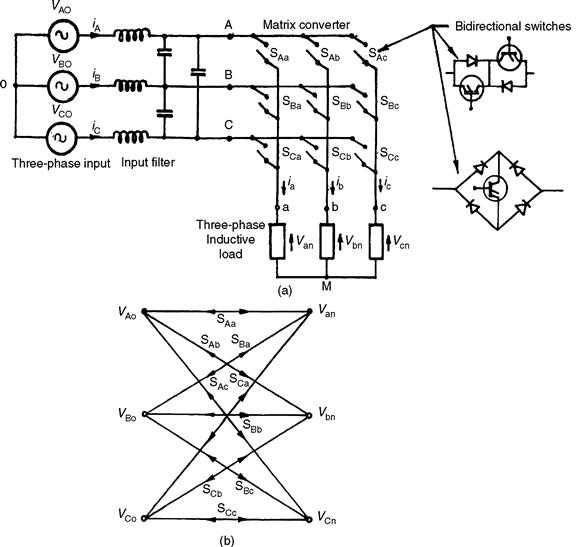
FIGURE 18.31 (a) 3ϕ-3ϕ Matrix converter (forced commutated cycloconverter) circuit with input filter and (b) switching matrix symbol for converter in (a).
18.5 Matrix Converter
The matrix converter (MC) is a development of the FCC based on bidirectional fully controlled switches, incorporating PWM voltage control, as mentioned earlier. With the initial progress made by Venturini [19–21], it has received considerable attention in recent years as it provides a good alternative to the double-sided PWM voltage source rectifier-inverters having the advantages of being a single stage converter with only nine switches for three-phase to three-phase conversion and inherent bidirectional power flow, sinusoidal input/output waveforms with moderate switching frequency, possibility of a compact design due to the absence of dc link reactive components, and controllable input power factor independent of the output load current. The main disadvantages of the matrix converters developed so far are the inherent restriction of the voltage transfer ratio (0.866), a more complex control, commutation and protection strategy, and above all the nonavailability of a fully controlled bidirectional high frequency switch integrated in a silicon chip (triac, though bilateral, cannot be fully controlled).
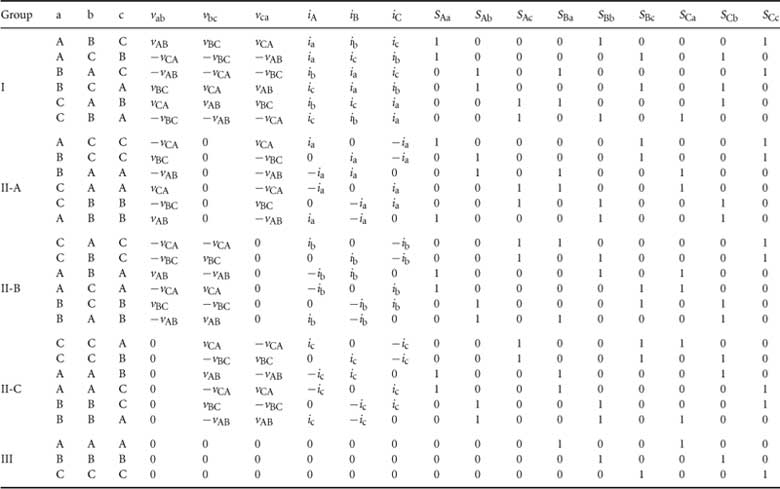
The power circuit diagram of the most practical three-phase to three-phase (3ϕ–3ϕ) matrix converter is shown in Fig. 18.31a which uses nine bidirectional switches so arranged that any of the three input phases can be connected to any output phase as shown in the switching matrix symbol in Fig. 18.31b. Thus, the voltage at any input terminal may be made to appear at any output terminal or terminals while the current in any phase of the load may be drawn from any phase or phases of the input supply. For the switches, the inverse-parallel combination of reverse-blocking self-controlled devices like power MOSFETs or IGBTs or transistor embedded diode bridge as shown have been used so far. New perspective configuration of the bidirectional switch is to use two RB-IGBTs with reverse blocking capability in antiparallel, eliminating the diodes reducing the conducting losses in the converter significantly. The circuit is called a matrix converter as it provides exactly one switch for each of the possible connections between the input and the output. The switches should be controlled in such a way that, at any time, one and only one of the three switches connected to an output phase must be closed to prevent “short circuiting” of the supply lines or interrupting the load current flow in an inductive load. With these constraints, it can be visualized that out of the possible 512 (= 29) states of the converter, only 27 switch combinations are allowed as given in Table 18.1 which includes the resulting output line voltages and input phase currents. These combinations are divided into three groups. Group-I consists of six combinations when each output phase is connected to a different input phase. In Group-II, there are three subgroups each having six combinations with two output phases short-circuited (connected to the same input phase). Group-III includes three combinations with all output phases short-circuited.
TABLE 18.1 Three-phase/three-phase matrix converter switching combinations
With a given set of input three-phase voltages, any desired set of three-phase output voltages can be synthesized by adopting a suitable switching strategy. However, it has been shown [21, 22] that regardless of the switching strategy, there are physical limits on the achievable output voltage with these converters as the maximum peak-to-peak output voltage cannot be greater than the minimum voltage difference between two phases of the input. To have complete control of the synthesized output voltage, the envelope of the three-phase reference or target voltages must be fully contained within the continuous envelope of the three-phase input voltages. Initial strategy with the output frequency voltages as references reported the limit as 0.5 of the input as shown in Fig. 18.32a. This can be increased to 0.866 by adding a third-harmonic voltage of input frequency (Vi/4) cos 3ωi t to all target output voltages and subtracting from them a third harmonic voltage of output frequency (Vo/6) cos 3ωo t as shown in Fig. 18.32b [21, 22]. However, this process involves considerable amount of additional computations in synthesizing the output voltages. The other alternative is to use the space vector modulation (SVM) strategy as used in PWM inverters without adding third harmonic components but it also yields the maximum voltage transfer ratio as 0.866.

FIGURE 18.32 Output voltage limits for three-phase ac–ac matrix converter: (a) basic converter input voltages and (b) maximum attainable with inclusion of third harmonic voltages of input and output frequency to the target voltages.
An ac input LC filter is used to eliminate the switching ripples generated in the converter and the load is assumed to be sufficiently inductive to maintain continuity of the output currents.
18.5.1 Operation and Control of the Matrix Converter
The converter in Fig. 18.31 connects any input phase (A, B, and C) to any output phase (a, b, and c) at any instant. When connected, the voltages van, vbn, vcn at the output terminals are related to the input voltages VAo, VBo, VCo as
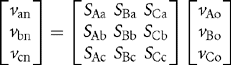 (18.32)
where SAa through SCc are the switching variables of the corresponding switches shown in Fig. 18.31. For a balanced linear star-connected load at the output terminals, the input phase currents are related to the output phase currents by
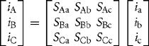 (18.33)
Note that the matrix of the switching variables in Eq. (18.33) is a transpose of the respective matrix in Eq. (18.32). The matrix converter should be controlled using a specific and appropriately timed sequence of the values of the switching variables, which will result in balanced output voltages having the desired frequency and amplitude, while the input currents are balanced and in phase (for unity IDF) or at an arbitrary angle (for controllable IDF) with respect to the input voltages. As the matrix converter, in theory, can operate at any frequency, at the output or input, including zero, it can be employed as a three-phase ac–dc converter, dc/three-phase ac converter, or even a buck/boost dc chopper and thus as a universal power converter.
The control methods adopted so far for the matrix converter are quite complex and are subjects of continuing research [21–38]. Out of several methods proposed for independent control of the output voltages and input currents, two methods are of wide use and will be briefly reviewed here: (1) the Venturini method based on a mathematical approach of transfer function analysis and (2) the space vector modulation (SVM) approach (as has been standardized now in the case of PWM control of the dc link inverter).
Venturini Method: Given a set of three-phase input voltages with constant amplitude Vi and frequency fi = ωi /2π, this method calculates a switching function involving the duty cycles of each of the nine bidirectional switches and generate the three-phase output voltages by sequential piecewise sampling of the input waveforms. These output voltages follow a predetermined set of reference or target voltage waveforms and with a three-phase load connected, a set of input currents Ii and angular frequency ωi should be in phase for unity IDF or at a specific angle for controlled IDF.
A transfer function approach is used in [29] to achieve the above-mentioned features by relating the input and output voltages and the output and input currents as
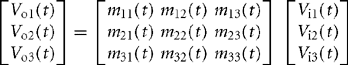 (18.34)
 (18.35)
where the elements of the modulation matrix, mij(t) (i, j = 1, 2, 3) represent the duty cycles of a switch connecting output phase i to input phase j within a sample switching interval. The elements of mij(t) are limited by the constraints
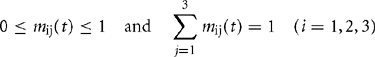
The set of three-phase target or reference voltages to achieve the maximum voltage transfer ratio for unity IDF is
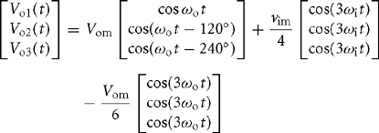 (18.36)
where Vom and Vim are the magnitudes of output and input fundamental voltages of angular frequencies ωo and ωi, respectively. With Vom ≤ 0.866 Vim, a general formula for the duty cycles mij (t) is derived in [29]. For unity IDF condition, a simplified formula is
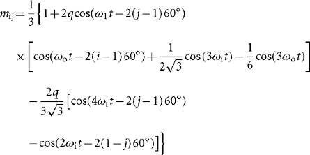 (18.37)
where i, j = 1, 2, 3 and q = Vom/Vim.
The method developed as above is based on a Direct Transfer Function (DTF) approach using a single modulation matrix for the matrix converter, employing the switching combinations of all the three groups in Table 18.1. Another approach called indirect transfer function (ITF) approach [23, 24] considers the matrix converter as a combination of PWM voltage source rectifier-PWM voltage source inverter (VSR–VSI) and employs the already well-established VSR and VSI PWM techniques for MC control utilizing the switching combinations of Group-II and Group-III only of Table 18.1. The drawback of this approach is that the IDF is limited to unity and the method also generates higher and fractional harmonic components in the input and the output waveforms.
SVM Method: The space vector modulation is a well-documented inverter PWM control technique which yields high voltage gain and less harmonic distortion compared to the other modulation techniques. Here, the three-phase input currents and output voltages are represented as space vectors and SVM is simultaneously applied to the output voltage and input current space vectors, while the matrix converter is modeled as a rectifying and inverting stage by the indirect modulation method (Fig. 18.33). Applications of SVM algorithm to control of matrix converters have appeared extensively in the literature [27–37] and shown to have inherent capability to achieve full control of the instantaneous output voltage vector and the instantaneous current displacement angle even under supply voltage disturbances. The algorithm is based on the concept that the MC output line voltages for each switching combination can be represented as a voltage space vector defined by
![]() (18.38)
(18.38)
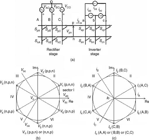
FIGURE 18.33 Indirect modulation model of a matrix converter: (a) VSR-VSI conversion; (b) output voltage switching vector hexagon; and (c) input current switching vector hexagon.
Out of the three groups in Table 18.1, only the switching combinations of Group-II and Group-III are employed for the SVM method. Group-II consists of switching state voltage vectors having constant angular positions and are called active or stationary vectors. Each subgroup of Group-II determines the position of the resulting output voltage space vector and the six state space voltage vectors form a six-sextant hexagon used to synthesize the desired output voltage vector. Group-III comprises the zero vectors positioned at the center of the output voltage hexagon and these are suitably combined with the active vectors for the output voltage synthesis.
The modulation method involves selection of the vectors and their on-time computation. At each sampling period Ts, the algorithm selects four active vectors related to any possible combinations of output voltage and input current sectors in addition to the zero vector to construct a desired reference voltage. The amplitude and the phase angle of the reference voltage vector are calculated, and the desired phase angle of the input current vector is determined in advance. For computation of the on-time periods of the chosen vectors, these are combined into two sets leading to two new vectors adjacent to the reference voltage vector in the sextant and having the same direction as the reference voltage vector. Applying the standard SVM theory, the general formulae derived for the vector on-times which satisfy, at the same time, the reference output voltage and input current displacement angle in [29] are
 (18.39)
where q is voltage transfer ratio, ϕi is the input displacement angle chosen to achieve the desired input power factor (with ϕi = 0, a maximum value of q = 0.866 is obtained), θo and θi are the phase displacement angles of the output voltage and input current vectors, respectively, whose values are limited within the 0–60° range. The on-time of the zero vector is
 (18.40)
The integral value of the reference vector is calculated over one sample time interval as the sum of the products of the two adjacent vectors and their on-time ratios and the process is repeated at every sample instant.
Control Implementation and Comparison of the Two Methods: Both the methods need a digital signal processor (DSP) based system for their implementation. In one scheme [29] for the Venturini method, the programmable timers, as available, are used to time out the PWM gating signals. The processor calculates the six switch duty cycles in each sampling interval, converts them to integer counts and stores them in the memory for the next sampling period. In the SVM method, an erasable programmable read only memory (EPROM) is used to store the selected sets of active and zero vectors and the DSP calculates the on-times of the vectors. Then, with an identical procedure as in the other method, the timers are loaded with the vector on-times to generate PWM waveforms through suitable output ports. The total computation time of the DSP for the SVM method has been found to be much less that of the Venturini method. Comparison of the two schemes shows that while in the SVM method the switching losses are lower, the Venturini method shows better performance in terms of input current and output voltage harmonics.
A direct control method as used in conjunction with the voltage source converters has been developed recently and implemented with a 10-kVA matrix converter [38].
18.5.2 Commutation and Protection Issues in a Matrix Converter
As the matrix converter has no dc link energy storage, any disturbance in the input supply voltage will affect the output voltage immediately and a proper protection mechanism has to be incorporated, particularly against over-voltage from the supply and over-current in the load side. As mentioned, two types of bidirectional switch configurations have hitherto been used, one, the transistor (now IGBT) embedded in a diode bridge and the other, the two IGBTs in antiparallel with reverse voltage blocking diodes. (shown in Fig. 18.31). In the latter configuration, each diode and IGBT combination operates in two quadrants only which eliminates the circulating currents otherwise built up in the diode bridge configuration that can be limited by only bulky commutation inductors in the lines.
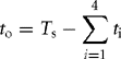
Commutation: The MC does not contain freewheeling diodes which usually achieve safe commutation in the case of other converters. To maintain the continuity of the output current as each switch turns off, the next switch in sequence must be immediately turned on. In practice, with bidirectional switches, a momentary short circuit may develop between the input phases when the switches cross-over and one solution is to use a semisoft current commutation using a multi-stepped switching procedure to ensure safe commutation [39–41]. This method requires independent control of each two quadrant switches, sensing the direction of the load current and introducing a delay during the change of switching states. The switching rule for proper commutation from S1 to S2 of the arrangement shown in Fig. 18.34 for iL > 0 with the two quadrant switches for four-stepped commutation [39, 41] is (a) turn off SIB, (b) turn on S2A, (c) turn off S1A, and (d) turn on S2B.
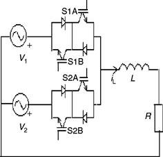
FIGURE 18.34 Safe commutation scheme.
Analogously, for iL < 0, the switching rule will be (a) turn off S1A, (b) turn on S2B, (c) turn off S1B, and (d) turn on S2A.
Typically, these commutation strategies are now implemented using programmable logic devices such as field programmable gate array (FPGA), programmable logic device (PLD) [41, 42], etc.
A robust voltage commutation scheme without sacrificing the line side current waveform quality and with minimal information requirement has been reported recently [43].
Protection Strategies: A clamp capacitor (typically 2 μF for a 3-kW permanent magnet (PM) motor) connected through two three-phase full-bridge diode rectifiers involving additional 12 diodes as shown in Fig. 18.35 (a new configuration has been reported in [44] where the number of additional diodes are reduced to six using the antiparallel switch diodes at the input and output lines of the MC) serves as a voltage clamp for possible voltage spikes under normal and fault conditions. A new passive protection strategy involving suppressor diodes and varistors for excellent over-voltage protection is discussed recently in [45], which allows the removal of the large and expensive diode clamp. A snubberless solution for over-voltage protection is presented in [46].
FIGURE 18.35 Diode clamp for matrix converter.
Input Filter: A three-phase single stage LC filter at the input consisting of three capacitors in star and three inductors in the line is used to adequately attenuate the higher order harmonics and render sinusoidal input current. Typical values of L and C based on a 415 V converter with a maximum line current of 6.5 A and a switching frequency of 20 kHz are 3 mH and 1.5 μF only [47]. The filter may cause minor phase-shift in the input displacement angle which needs correction.
Figure 18.36 shows typical experimental waveforms of output line voltage and line current of an MC. The output line current is mostly sinusoidal except a small ripple, when the switching frequency is around 1 kHz only.
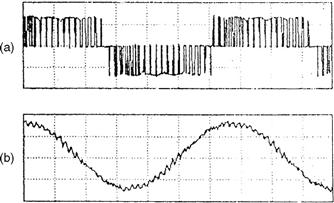
FIGURE 18.36 Experimental waveforms for a matrix converter at 30-Hz frequency from a 50-Hz input: (a) output line voltage and (b) output line current.
18.5.3 Multilevel Matrix converter
Erickson and Al-Naseem [48] introduced a multilevel matrix converter with four-quadrant dc link H-bridge switching cells as shown in Fig 18.37 in 2001. These are suitable for medium or high voltage ac-to-ac power conversion. The use of four transistors in the switch cell of Fig. 18.37a allows the average current to be doubled, relative to the conventional matrix converter whose four-quadrant switches are realized using two transistors and two diodes. With dc capacitor, the switch cell is capable of producing instantaneous voltages +V, 0, –V. These converters can both increase and decrease the voltage amplitude with arbitrary power factors. With series connection of switch cells in each branch of the matrix, multilevel switching can be attained with device voltages locally clamped to dc capacitor voltages. Several types of multilevel matrix converter topologies have been proposed, over the years, including a novel capacitor-clamped one and with space vector modulation [49, 50]. In [50], the converter utilizes flying capacitors to balance voltage distribution of series connected bidirectional switches and provide middle voltage levels.
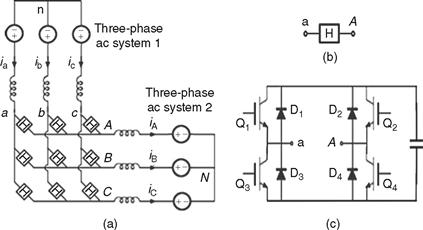
FIGURE 18.37 Multilevel matrix converter (a) configuration (b) switch symbol and (c) switch realization.
Recently, with cascaded combination of multiple MC (Matrix Converter) modules, principles of high power multi-modular matrix converters (MMMCs) built from three-input two-output matrix converter (3 × 2 MC) have been presented in [51] with modulation schemes to synthesize sinusoidal wave forms on both sides of the converters. These topologies feature modular design, bidirectional power flow and enable the use of low-voltage power devices. They may serve as potential candidates for high power applications where regenerative capability and power density are of importance. However, the drawbacks of them are large number of devices and the use of the input transformer.
18.5.4 Sparse Matrix Converter
As described in [52], sparse matrix converters (SMC) are functionally equivalent to conventional matrix converters (CMC) but based on the structure of an indirect matrix converter (IMC), Fig 18.38, with possibilities of a reduced number of power devices and less control complexity. A CMC as shown in 18.31a requires 9 bidirectional switches, usually constructed using 18 IGBTs, to switch the three input phases between the three out phases. The SMC (Fig. 18.39) is derived from the IMC which is split into an input stage and output stage without any capacitance in the DC Link. The input stage is arranged so that only 9 switches are required, while the output stage has a standard 6 switch configuration. Thus, the SMC has a total of 15 switches compared to 18 for a CMC. The functional equivalence, the controllability and the operating range of the SMC is the same as CMC despite the reduced number of unipolar turn-off power switches [52]. Further reduction of the number of IGBTs is possible with Ultra sparse matrix converter (USMC) [53], Fig. 18.40 having 12 IGBTs, with restricted operation to a unidirectional power flow and controllability of the phase displacement of input voltage and current fundamental to ±π/6 [53]. Very recently, a space vector modulation scheme for an indirect 3-level sparse matrix converter (I3 SMC), which is a combination of a three-level neutral clamped voltage source inverter and an indirect matrix converter has been discussed in [54]. A 100-kHz SiC sparse matrix converter using 1300-V, 4-A SiC JFET cascade devices have been reported in [55] which is suitable for aircraft applications where a low volume/weight converter is desired.
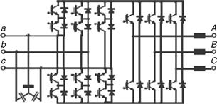
FIGURE 18.38 Indirect matrix converter (IMC).
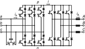
FIGURE 18.39 Sparse matrix converter (SMC).
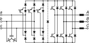
FIGURE 18.40 Ultra sparse matrix converter (USMC).
18.6 High Frequency Linked Single-Phase to Three-Phase Matrix Converters
Several kinds of single-phase to three-phase high frequency (typically, 20 kHz) cycloconverters (actually, matrix converters with MCT switches) using “soft switching” were reported for ac motor drive applications [56–58]. Figure 18.41 [56] shows a typical configuration of such a converter in which an H-bridge inverter produces a high-frequency single-phase voltage, which is fed to the cycloconverter through a high-frequency transformer. The high frequency ac may be either sinusoidal generated by a resonant link inverter or quasi-square wave as shown. These systems have been developed at laboratories but not yet available commercially [56].
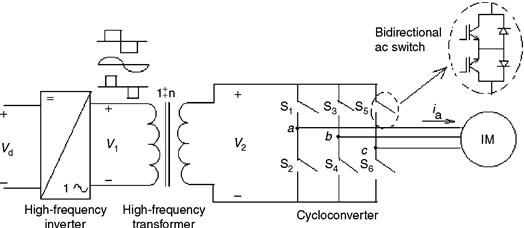
FIGURE 18.41 High frequency linked single-phase to three-phase matrix converter.
18.6.1 High Frequency Integral-Pulse Cycloconverter
The input to these converters maybe sinusoidal or quasi-square wave and it is possible to use integral half-cycle pulse width modulation (IPM) principle to synthesize the output voltage waves. The advantage is that the devices can be switched at zero voltage reducing the switching loss. This converter can only work at output frequency, which are multiples of the input frequency [56].
18.6.2 High-Frequency Phase-Controlled Cycloconverter
Here, phase control principle as explained earlier is used to synthesize the output voltage. A sawtooth carrier wave is compared with the sine modulating wave to generate the firing instants of the switches. The phase control provides switching at zero current reducing switching loss but this scheme has more complex control circuit compared to the previous one. However, it can work at any frequency [57].
18.7 Applications of AC–AC Converters
18.7.1 Applications of AC Voltage Controllers
AC voltage controllers are used either for control of the rms value of voltage or current in lighting control, domestic and industrial heating, speed control of fan, pump or hoist drives, soft starting of induction motors, etc. or as static ac switches (on/off control) in transformer tap changing, temperature control, speed stabilization of high inertia induction motor drives like centrifuge, capacitor switching in static reactive power compensation, etc.
In fan or pump drives with induction motors, the torque varies as the square of the speed. So the speed control is required in a narrow range and an ac voltage controller is suitable for an induction motor with a full load slip of 0.1–0.2 in such applications. For these drives, braking or reverse operations are not needed but for the crane hoist drive, both motoring and braking are needed and a four quadrant ac voltage controller can be obtained by a modification of the ac voltage controller circuit as shown in Fig. 18.42. SCR pairs A, B, and C provide operation in quadrants I and IV and A, B, and C in quadrants II and III. While changing from one set of SCR pairs to another, care should be taken to ensure that the incoming pair is activated only after the outgoing pair is fully turned off.
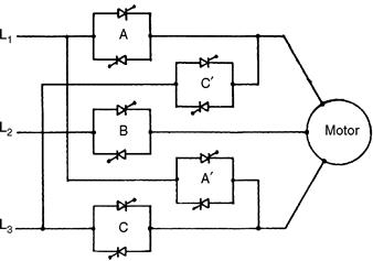
FIGURE 18.42 Four quadrant ac voltage controller.
AC voltage controllers are being increasingly used for soft-starting of induction motors, as they have a number of advantages over the conventional starters such as smooth acceleration and deceleration, ease in implementation of current control, simple protection against single-phasing or unbalanced operation, reduced maintenance and losses, absence of current inrush, etc. Even for the fixed-speed industrial applications, the voltage controllers can be used to provide a reduced stator voltage to an induction motor to improve its efficiency at light load and result in energy saving. Operation at an optimum voltage reduces the motor flux which, in turn, reduces the core-loss and the magnetizing component of the stator copper loss. Considerable savings in energy can be obtained in applications where a motor operates at no load for a significant time such as in drills, machine tools, woodworking machines, reciprocating air-compressors, etc. A popular approach to find an optimum operating voltage is to maximize the motor power factor by maintaining a minimum phase-shift between the voltage and current after sensing them.
The ac switch with on/off control used in driving a high inertia centrifuge involves switching on of the motor when the speed of the centrifuge drops below the minimum allowable level and switching off when the speed reaches the maximum allowable level –thus maintaining a constant average speed. An identical scheme of control is used with an ac switch for temperature control of an electric heater or air conditioner.
Integral cycle control is well suited to heating control while it may cause flicker in normal incandescent lighting control and speed fluctuations in motor control. However, with this control, less voltage distortion is produced in the ac supply system and less radio-frequency interference is propagated when compared with the phase-controlled system.
18.7.2 Applications of Cycloconverters
Cycloconverters as frequency changers essentially find well-established applications in (1) high-power low-speed reversible ac motor drives with constant-frequency input; and (2) constant-frequency power supplies with a variable-frequency input as in VSCF (variable-speed constant frequency) system, whereas they find potential applications in (3) controllable VAR (volt-amperes reactive) generators for power factor correction; and (4) ac system interties linking two independent power systems as demonstrated in [15].
Variable Speed AC Drives: In this category, the applications of cycloconverter-controlled induction motor and synchronous motor drives have been adequately reviewed in [9]. Cycloconverter-fed synchronous motors are well suited for low-speed drives with high torque at standstill, and high-capacity gear-less cement mills (tube or ball-mill above 5 MW) have been the first applications of these drives.
Since 1960s, as developed by Siemens and Brown Boveri, one of the early installations employs a motor rating of 6.4 MW having a rotor diameter of 5 m and length of 18.5 m, whereas the stator construction is similar to that of a hydroelectric generator with 44 poles requiring 5.5 Hz for maximum speed of 15rpm. The motor is flanged with the mill cylinder without additional bearings or “wrapped” directly around it, known as ring motor [59]. With the evolution of field orientation or vector control, cycloconverter-fed synchronous motors have replaced or are replacing the dc drives in the reversing rolling mills (2/4 MW) with extreme high-dynamic requirements for torque and speed control [60–62], in mine winders and haulage [62, 63] of similar high ratings and in icebreakers and ships equipped with diesel generators with power ratings of about 20 MW/unit [64]. In these applications, the cycloconverter-fed synchronous motor is in self-controlled mode and known as ac commutator-less motor when the cyclo-converter firing signals are derived from a rotor shaft position sensor, so that the frequency is slaved to the rotor speed and not vice versa with the result that the hunting and stability problems are eliminated and the torque is not limited to pull-out value. Further, with field control, the motor can be operated at leading power factor when the cycloconverter can operate with load commutation from the motor side at high speed in addition to the line commutation from the supply at low speed, thus providing speed control over a wide range. A cycloconverter-fed ac commutator-less motor is reported in [65] where the cycloconverter is operated both in sinusoidal and trapezoidal mode –the latter is attractive for better system power factor and higher voltage output at the cost of increased harmonic content [1]. A stator-flux oriented vector control scheme for a six-pulse circulating current-free cycloconverter-fed synchronous motor with a flux observer suitable for a rolling mill drive (300–0–300 rpm) is reported in [12]. A 12-pulse, 9.64-MVA, 120/33.1-Hz cycloconverter-linear synchronous motor combination for Maglev Vehicle ML-500, a high-speed train, (517 km/h) is in the process of development in Japan since early 1980s [66]. Several recent projects involving very high-power (larger than 15 MW) semiautogenous grinding (SAG) mills with cycloconverter-fed synchronous motor drives in mining applications in peru and Brazil are reported in [67]. Latest technological advances, applications, and future trends of cycloconverters in industrial medium voltage drives have been discussed in [68].
Regarding cycloconverter-fed induction motors, early applications were for control of multiple run-out table motors of a hot strip mill, high performance servo drives, and controlled slip-frequency drive for diesel electric locomotives. Slip-power controlled drives in the form of static Scherbius drives with very high ratings using cycloconverter in the rotor of a doubly fed slip-ring induction motor have been in operation for high capacity pumps, compressors [69], and even in a proton–synchrotron accelerator drive in CERN, Geneva [70]. Though synchronous motors have been preferred for very high-capacity low-speed drives because of their high rating, ability to control power factor, and precisely set speed independent of supply voltage and load variations, induction motors, because of their absence of excitation control loop, simple structure, easy maintainability, and quick response, have been installed for cycloconverter-fed drives in Japan. For example, a seemless tube piercing mill [71] where a squirrel cage 6-pole 3-MW, 188/300-rpm, 9.6/15.38-Hz, 2700-V motor is controlled by a cycloconverter bank of capacity 3750 KVA and output voltage 3190 V.
Constant Frequency Power Supplies: Some applications such as aircraft and naval ships need a well-regulated constant-frequency power output from a variable-frequency ac power source. For example, in aircraft power conversion, the alternator connected to the engine operating at a variable speed of 10,000–20,000 rpm provides a variable frequency output power over 1200–2400 Hz range which can be converted to an accurately regulated fixed frequency output power at 400 Hz through a cycloconverter with a suitable filter placed within a closed loop. The output voltages of the cycloconverter are proportional to the fixed frequency (400 Hz) sine wave reference voltage generator in the loop.
Both synchronous and induction motors can be used for VSCF generation. The static Scherbius system can be modified (known as Kramer drive) by feeding slip-power through a cycloconverter to a shaft mounted synchronous machine with a separate exciter for VSCF generation. A new application in very high power ratings of constant frequency variable speed motor generators with cycloconverter is in pumped storage schemes using reversible pump turbines for adaptation of the generated power to varying loads or keeping the ac system frequency constant. In 1993, a 400 MW variable speed pumped storage system was commissioned by Hitachi at Okhawachi hydropower plant [72] in Japan where the field windings of a 20-pole generator/motor are excited with three-phase low-frequency ac current via slip-rings by a 72-MVA, three-phase 12-pulse line-commuted cycloconverter. The armature terminals rated at 18 kV are connected to a 500-kV utility grid through a step-up transformer. The output frequency of the circulating current-free cycloconverter is controlled within ± 5 Hz and the line frequency is 60 Hz. The variable speed system has a synchronous speed of 360 rpm with a speed range 330 –390 rpm. The operational system efficiency in the pump mode is improved by 3% when compared to the earlier constant speed system.
Static VAR Generation: Cycloconverters with a high frequency (HF) base, either a HF generator or an oscillating LC tank, can be used for reactive power generation and control, replacing synchronous condensers or switched capacitors as demonstrated in [15]. If the cycloconverter is controlled to generate output voltage waves whose wanted components are in phase with the corresponding system voltages, reactive power can be supplied in either direction to the ac system by amplitude control of the cycloconverter output voltages. The cycloconverter will draw leading current from (that is, it will supply lagging current to) the ac system when its output voltage is greater than that of the system voltage and vice versa.
Interties between AC Power Systems: The naturally commutated cycloconverter (NCC) was originally developed for this application to link a three-phase, 50-Hz ac system with a single-phase 16![]() -Hz railway supply system in Germany in the 1930s. Applications involve slip-power controlled motors with sub-synchronous and super-synchronous speeds. The stator of the motor is connected to 50-Hz supply, which is connected to the rotor as well as through a cycloconverter, and the motor drives a single-phase synchronous generator feeding to 16
-Hz railway supply system in Germany in the 1930s. Applications involve slip-power controlled motors with sub-synchronous and super-synchronous speeds. The stator of the motor is connected to 50-Hz supply, which is connected to the rotor as well as through a cycloconverter, and the motor drives a single-phase synchronous generator feeding to 16![]() -Hz system [73, 74]. A static asynchronous intertie between two different systems of different frequency can be obtained by using two NCCs in tandem, each with its input terminals connected to a common HF base. As long as the base frequency is appropriately higher than that of the either system, two system frequencies can be either same or different. The power factor at either side can be maintained at any desired level [15].
-Hz system [73, 74]. A static asynchronous intertie between two different systems of different frequency can be obtained by using two NCCs in tandem, each with its input terminals connected to a common HF base. As long as the base frequency is appropriately higher than that of the either system, two system frequencies can be either same or different. The power factor at either side can be maintained at any desired level [15].
18.7.3 Applications of Matrix Converters and New Developments
The practical applications of the matrix converters, as of now, are very limited. The main reasons are (1) non-availability of the bilateral fully controlled monolithic switches capable of high frequency operation; (2) complex control law implementation; (3) an intrinsic limitation of the output/input voltage ratio; and (4) commutation and protection of the switches. Till date, the switches are assembled from existing discrete devices resulting in increased cost and complexity, and only experimental circuits of conventional matrix converters (CMC) of capacity upto 150 kVA [75] for a single unit have been built. However, with the advances in device technology, it is hoped that the problems will be solved eventually, and the MC will not only replace the NCCs in all the applications mentioned under Section 18.7.2, but also take over from the PWM rectifier-inverters as well. Already, interesting applications of multilevel and multicell matrix converters for medium-voltage high-power drives have been developed [76] Super energy-saving multicell medium-voltage matrix converters (FSDrive-MX1S) of rating 3 kV, 200–3000 kVA or 6 kV, 400–6000 kVA have been built by Yaskawa Electric, Japan [77] where by intelligently phase-shifting the carrier of each cell and combining them in the motor windings, medium-voltages are achievable as shown in Fig. 18.43. The salient features of these medium voltage converters are as follows:
• Excellent input current waveform due to multiple phase shifting winding of the input transformer;
• Flexible design: Three cells in series yielding 3.3 kV, 200–3000 kVA and six cells in series yielding 6 kV, 400–6000 kVA system;
• Excellent output voltage waveform due to multi-step configuration.
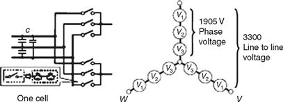
FIGURE 18.43 Schematic of a multicell matrix converter with 3 cells in series in each phase.
The applications for these drives as recommended are as follows: with heavy loads that require regenerative energy such as steel manufacturing process lines or cargo handling machinery, and also that need power regeneration for a long period such as winders for paper.
Recently, reverse blocking IGBTs have opened up the possibility of bidirectional switch (BDS) construction for a practical matrix converter with just two back-to-back devices [78–80]. A compact full matrix converter power module EconoMac [81] in a single package using 18 IGBT devices (35 A, 1200 V) and diodes in the common collector configuration (Fig. 18.44) is available with Eupec/Siemens, Germany. This packaging minimizes the stray inductance in the current commutation paths. Fuji and Powerex have developed engineering samples for matrix converter output leg in a module using RB-IGBTs. Anewpower electronic building block (PEBB) configuration for a low cost MC has been proposed in [82]. Recently, an efficient approach to design discrete packaging of bidirectional resonant power switch for matrix converters has been proposed by computing the magnetic field orientation inside the switching cell [83]. Several new concepts in protection, commutation, switch design, and modulation strategy have been presented in [84].
FIGURE 18.44 EconoMac matrix converter module by Eupec [81].
Several new methods like overmodulation [85], adaptive rate regulation [86], and two-side modulation control [87] have been introduced with experimental results to achieve higher voltage transfer ratio. A matrix converter-based three-phase open-end winding ac machine drive having matrix converters, one at each side of the open-end winding with space vector PWN has been recently described in [88] to achieve several simultaneous benefits, such as converter voltage gain up to 1.5, controllable grid power factor, and elimination of the high-frequency common-mode voltage at the machine terminals. A generalized scalar PWM (GSPWM) technique to reduce the common-mode voltage in matrix converter without degrading the input currents’ quality has been studied in a recent paper [89].
Design and loss comparison of matrix converters and dc-link voltage source converters (VSC) have been discussed in [90, 91]. It is shown that although MC requires 50% more semiconductors and gate drives excluding clamp circuit, the active silicon area and the number of gate unit power supplies are comparable to that of VSC of the same power rating. The losses of both converter systems are roughly the same at the typical range of 40–70% of rated torque and speed and a switching frequency of 10 kHz. The MC realizes a distinct better efficiency (92.5–96%) at 100% torque compared with VSC for the same IGBT modules. Also, the maximum switching frequency of the MC (30 kHz at 250% rated torque) is also substantially higher. The low losses allow a reduction of current ratings (by 33%) of IGBT modules in MC. The extra harmonic losses due to use of a matrix converter for a motor drive with two commonly used modulation techniques have been computed and compared in [92].
Various potential applications of matrix converters have been proposed, and experiments conducted in the field of VSCF systems such as wind-turbine and micro-turbine [93], switched mode power supplies [94], doubly fed induction motor [95, 96] including wind power system applications [97], and marine propulsion [98]. Few modern solutions for industrial matrix converter applications including a new integrated matrix converter motor (MCM) have been reported [99, 100]. The range of published practical implementations varies from a 2-kW matrix converter using silicon carbide devices and switching at 150 kHz for aerospace applications built at ETZ in Zurikh, Switzerland to a 150 kVA converter using 600 A IGBTs built at US army research labs in collaboration with the University of Nottingham, UK [42, 75]. A matrix converter using MCTs with enhanced commutation times is described in [101].
The complex control schemes of matrix converter demand higher test requirements and one of the modern means of testing the controllers before final integration on actual apparatus is to make hardware-in-the-loop (HIL) real-time simulation tests as developed recently [102].
Matrix converter-fed adjustable speed drives (ASDs) have the advantages of inherent four-quadrant operation, absence of bulky dc-link electrolytic capacitors, clean input power characteristics with high input power factor and increased power density with the possibilities of operating at higher temperatures. However, due to the absence of the dc link, these are more susceptible to input power disturbances and a ride-through module is needed to be added for these drives under short-term power interruption. Such a module as developed with minimal addition of hardware and software into a matrix converter (230 V, 3kVA) has been reported in [103]. A PWM modulation strategy for fault tolerant operation of the matrix-converter-based drives against opened switch, opened phase faults, and shorted winding failures has been proposed in [104]. This can improve the reliability of the matrix converter drives as it is possible to keep continuous by regulating the two remaining phases after isolating the faulted phase.
A novel application of a three-phase matrix converter as the static conversion unit for a ground power-supply unit for aircraft servicing has been presented in [105] to provide a compact solution with no dc link and the capability to generate a high quality 400-Hz sinusoidal waveformin the steady state. A new type of single phase Z-source buck-boost matrix converter has been proposed in [106], which can be used in various industrial applications that require step-changed frequencies and variable voltage amplitudes. A direct ac–ac current source matrix converter for applications in industrial power systems is introduced in [107]. A dynamic voltage restorer (DVR) system employing matrix converter and flywheel storage has been proposed in [108] to cope with voltage sag problem in power system. The proposed topology eliminates the dc-link passive components resulting in reduced maintenance requirement and improved power density.
REFERENCES
1. Rombaut C, Seguier G, Bausiere R. Power Electronic Converters—AC/AC Conversion. New York: McGraw-Hill; 1987.
2. Shepherd W. Thyristor Control of AC Circuits. Great Britain: Granada Publishing; 1975.
3. Trzynadlowski AM. Introduction to Modern Power Electronics. New York: John Wiley; 1998.
4. Rashid M. Power Electronics: Circuits, Devices and Applications. New Jersey: Prentice Hall; 1993.
5. Hart DW. Introduction to Power Electronics. New Jersey: Prentice Hall; 1997.
6. Chattopadhyay AK, Das SP, Karchowdhury S. Computer simulation of three-phase thyristor regulator-fed static and induction motor loads-A generalised approach. Electric Machines and Power Systems. 1993; vol. 21:329–342.
7. Dewan SB, Straughen A. Power Semiconductor Circuits. New York: John Wiley; 1975.
8. Pelly BR. Thyristor Phase-Controlled Converters and Cycloconverters. New York: John Wiley; 1971.
9. Chattopadhyay AK. Cycloconverters and cycloconverter-fed drives—A Review. J. Indian Inst. Sci.. September/October 1997; vol. 77:397–419.
10. Chattopadhyay AK, Rao TJ. Simplified control electronics for a practical cycloconverter. Int. J. Electronics. 1977; vol. 43:137–150.
11. Bird BM, Ford JS. Improvements in phase-controlled circulating current cycloconverters using communication principles. Proc. IEE. 1974; vol. 121(no. 10):1146–1149.
12. Das SP, Chattopadhyay AK. Observer based stator flux oriented vector control of cycloconverter-fed synchronous motor drive. IEEE Trans Ind. Appl.. July/August 1997; vol. IA-33(no. 4):943–955.
13. Syam P, Nandi PK, Chattopadhyay AK. An improvement feedback technique to suppress sub-harmonics in a naturally commutated cycloconverter. IEEE Trans. Ind. Electron.. December 1998; vol. 45(no. 6):950–952.
14. Syam P, Nandi PK, Chattopadhyay AK. Improvement in power quality and a simple method of subharmonic suppression for a cycloconverter-fed synchronous motor drive. IEE Proc. Elec. Power Appl.. July 2002; vol. 149(no. 4):292–303.
15. Gyugi L, Pelly BR. Static Power Frequency Changers: Theory, Design and Applications. New York: Wiley-Interscience; 1976.
16. Chattopadhyay AK, Rao TJ. Methods of digital computation of phase controlled cycloconverter performance. In: Conf. Rec. IEEEIAS Ann. Meet. 1978: 432–439.
17. Lin Y, Heydt GT, Chu RF. The power quality impact of cycloconverter control strategies. IEEE Trans. Power Delivery. April 2005; vol. 2(no. 2):1711–1718.
18. Loskarn M, Tost KD, Unger C, Witzmann R. Mitigation of Interharmonics due to large cycloconverter-fed mill drives. In: Proc. ICHQP’ 98. October 1998: 122–126.
19. Venturini M. A new sine-wave in sine-wave out converter technique eliminates reactor elements. Proc. POWERCON’ 80. 1980; vol. E3-1 [pp. E3-1-E3-15].
20. Alesina A, Venturini M. The generalised transformer: A new bidirectional waveform frequency converter with continuously adjustable input power factor. In: Proc. IEEE - PESC’ 80. 1980: 242–252.
21. Alesina A, Venturini M. Analysis and design of optimum amplitude nine-switch direct ac–ac converters. IEEE Trans. Power Electron.. January 1989; vol. 4(no. 1):101–112.
22. Holmes DG, Lipo TA. Implementation of a controlled rectifier using ac–ac matrix converter theory. IEEE Trans. Power Electronics. January 1992; vol. 7(no. 1):240–250.
23. Ziogas PD, Khan SI, Rashid M. Some improved forced commutated cycloconverter structures. IEEE Trans. Ind. Appl.. July/August 1985; vol. Ia-21:1242–1253.
24. Ziogas PD, Khan SI, Rashid M. Analysis and design of forced commutated cycloconverter structures and improved transfer characteristics. IEEE Trans. Ind. Electron.. August 1986; vol. IE-33(no. 3):271–280.
25. Neft CL, Schauder CD. Theory and design of a 30 HP matrix converter. In: Conf. Rec IEEE-IAS Ann. Meet. 1988: 248–253.
26. Ishiguru A, Furuhashi T, Okuma S. A novel control method of forced commutated cycloconverters using instantaneous values of input line voltages. IEEE Trans. Ind. Electron. June 1991; vol. 38(no. 3):166–172.
27. Huber L, Borojevic D, Burany N. Analysis, design and implementation of the space-vector modulator for forced commutated cycloconverters. IEE Proc. B. March 1992; vol. 139(no. 2):103–113.
28. Huber L, Borojevic D. Space vector modulated three-phase to three-phase matrix converter with input power factor correction. IEEE Trans. Ind. Appl.. November/December 1995; vol. 31:1234–1246.
29. Zhang L, Watthanasarn C, Shepherd W. Analysis and comparison of control strategies for ac–ac matrix converters. IEE Proc. Power Elec. Appl.. July 1998; vol. 145(no. 4):284–294.
30. Casadei D, Serra G, Tani A. Reduction of the input current harmonic content in matrix converters under input/output unbalance. IEEE Trans Ind. Appl.. June 1998; vol. 45(no. 3):401–411.
31. L. Zhang and C. Watthanasarn, “An efficient space vector modulation algorithm for ac–ac matrix converters: Analysis and implementation” IEE Conf Proc. 6th PEVD ’ 96, pp. 103–113.
32. Wheeler PW, Rodriguez J, Clare JC, Emperngen L, Wenstein A. Matrix converters: A technology review. IEEE Trans. Industrial Electronics. April 2002; vol. 49(no. 2):276–288.
33. Casadei D, Serra G, Tani A, Zarri L. Matrix converter modulation strategies: A new general approach based on space vector representation of the switch state. IEEE Trans Ind. Electron.. April 2002; vol. 49(no. 2):370–381.
34. Cha HJ, Enjeti PN. An approach to reduce common mode voltage in matrix converter. IEEE Trans. Ind. Appl.. July/August 2003; vol. 39:1151–1159.
35. Jussila M, Salo M, Tuusa H. Realization of a three-phase indirect matrix converter with an indirect vector modulation method. IEEE-PESC’ 2003. 2003; vol. 2:689–694.
36. Sun K, Huang L, Matsuse K, Ishida T. Combined control of matrix converter fed induction motor drive system. Proc. IEEE-IAS Ann. Meet. 2003; vol. 3:1723–1729.
37. Havrila R, Dobrucky B, Balazovic P. Space vector modulated three-phase to three-phase matrix converter with unity power factor. In: 2000: 103–108. EPE-PEMC2000 Conf. Rec.; vol. 2.
38. Mutschler P, Marcks M. A direct control method for matrix converters. IEEE Trans. Ind. Electron.. April 2002; vol. 49(no. 2):362–369.
39. Burany N. Safe control of four-quadrant switches. In: Conf. Rec IEEE-IAS Ann Meet. 1989: 1190–1194.
40. Kwon BH, Min BD, Kim JH. Novel commutatation techniques of ac–ac converters. IEE Proc. Elec. Power Appl.. July 1998; vol. 145(no. 4):295–300.
41. Sun Y, Xu F, Sun K. Design of matrix converter with bidirectional switches. Proc. IEEE-POWERCON’ 2002. October 2002; vol. 2:1034–1038.
42. Clare J, Wheeler P. New technology: Matrix converters. Industrial Electronics Society Newsletter. March 2005; vol. 52(no. 1):10–12.
43. Wei L, Lipo TA, Chen H. Robust voltage commutation of conventional matrix converter. Proc. IEEE-PESC’ 03. 2003; vol. 2:717–722.
44. Nielson P, Blabjerg F, Pederson JK. New protection issues of a matrix converter: Design considerations for adjustable-speed drives. IEEE Trans. Ind. Appl.. September/October 1999; vol. 35(no. 5):1150–1161.
45. Mahlein J, Bruckmann M, Braun M. Passive protection strategy for a drive system with a matrix converter and an induction machine. IEEE Trans. Ind. Electronics. April 2002; vol. 49(no. 2):297–303.
46. Simon O, Bruckmann M. Control and protection strategies for matrix converters. In: Proc. PCIM Conf. Rec.. 2000.
47. Wheeler P, Grant D. Optimized input filter design and low-loss switching techniques for a practical matrix converter. IEE Proc. Elec. Power Appl.. January 1997; vol. 144(no. 1):53–59.
48. Erickson RW, Al-Naseem OA. A new family of matrix converters. Proc. IEEE-IECON’ 01. 2001; vol. 2:1515–1520.
49. Wheeler P, Lie X, Lee MY, Emperingham L, Kunpner C, Clare J. A review of multi-level matrix converter technologies. Proc. IET- PEMD’ 08. 2008; 286–290.
50. Shi Y, Yang X, He Q, wang Z. Research on a novel capacitor clamped multilevel matrix Converter. IEEE Trans. Power Electronics. September 2005; vol. 20(no. 5):1055–1065.
51. Wang J, Wu B, Zargari NR. High power multi-modular matrix converters with sinusoidal Input/output waveforms. Proc IEEE-IECON’ 09. 2009; 542–547.
52. Kolar JW, Baumann M, Shafmeister F, Ertl H. Novel three-phase AC-DC-AC sparse matrix converter—Part 1: Derivation, Basic principle of operation, Space vector modulation, Dimensioning. Proc IEEE-APEC’ 02. 2002; 777–787.
53. Kolar JW, Schafmeister F, Round SD, Ertl H. Novel three-phase AC–AC sparse matrix converters. IEEE Trans. Power Electronics. September 2007; vol. 22(no. 5):1649–1661.
54. Lee MY, Wheeler P, Klumpner C. Space vector modulated multilevel matrix converter. IEEE Trans. Ind Electronics. 2010.
55. Friedli T, Round SD, Kolar JW. A 100 kHz SiC sparse matrix converter. Proc. IEEE -PESC’ 07. 2007; 2148–2154.
56. Hui L, Ozpineci B, Bose BK. A soft-switched high frequency non-resonant link integral pulse modulated dc-ac converter for ac motor drive. In: 1998: 726–732. Proc. IEEE-IECON; vol. 2.
57. Ozpineei B, Bose BK. Soft-switched performance based high frequency non-resonant link phase-controlled converter for ac motor drive. In: 1998: 733–739. Proc. IEEE-IECON; vol. 2.
58. Bose BK. Modern Power Electronics and AC Drives. New Delhi: Pearson Education; 2002.
59. Blauenstein E. The first gearless drive for a tube mill. Brown Boveri Review. 1970; vol. 57:96–105.
60. Timpe W. Cycloconverter for rolling mill drives. IEEE Trans. Ind. Appl.. 1982; vol. IA-18(no. 4):401–404.
61. Pallman RP. First use of cycloconverter-fed ac motors in an aluminium hot strip mill. Siemens Engineering & Automation. 1992; vol. XIV(no. 2):26–29.
62. Lewis EA. Cycloconverter drive systems. IEE Conf. Proc. PEVD’ 96. 1996; 382–389.
63. Madisetti K, Ramlu MA. Trends in electronic control of mine hoists. IEEE Trans. Ind. Appl.. 1986; vol. IA-22(no. 6):1105–1112.
64. Hill AW, Turton RAV, Dunzan RL, Schwaln CL. A vector controlled cycloconverter drive for an ice-breaker. IEEE Trans. Ind. Appl.. November/December 1987; vol. IA-23:1036–1041.
65. Das SP, Chattopadhyay AK. Comparison of simulation and test results for an ac commutatorless motor drive. IEE Conf. Proc. PEVD’ 96. 1996; 294–299.
66. Saijo T, Koike S, Takaduma S. Characteristics of linear synchronous motor drive cycloconverter for Maglev Vehicle ML-500 at Miyazaki test track. IEEE Trans. Ind. Appl.. 1981; vol. IA-17:533–543.
67. Rodriguez JR, Pontt J, Newman P, Musalem R, Miranda H, Moran L, Azamora G. Technical evaluation and practical experience of high power grinding mill drives in mine applications. IEEE Trans. Ind. Appl.. May/June 2005; vol. 41(no. 3):866–873.
68. Wu B, Pontt J, Rodriguez J, Bernett S, Kouro S. Current source converter and cycloconverter topologies for industrial medium- voltage drives. IEEE Trans. Ind. Electronics. July 2008; vol. 55(no. 7):2786–2797.
69. Weiss HW. Adjustable speed ac drive systems for pump and compressor applications. IEEE Trans. Ind. Appl.. 1975; vol. IA-10(no. 1):162–167.
70. Dirr R, Neuffer I, Schluter W, Waldmann H. New electronic control equipment for doubly-fed induction motors of high rating. Siemens Review. 1972; vol. 3:121–126.
71. Sugi K, Naito Y, Kurosawa P, Kano Y, Katayama S, Yashida T. A microcomputer based high capacity cycloconverter drive for main rolling mill. In: Proc. IPEC. 1983: 744–755.
72. Mori S, Kita E, Kojima H, Sanematru T, Shiboya A, Bando A. Commissioning of 400 MW adjustable speed pumped storage system at Okhawachi hydropower plant. In: Proc. 1995 CIGRE Symp.. 1995. [no. 520–04].
73. Stemmler H. High power industrial drives. Proc. IEEE. August 1994; vol. 82(no. 8):1266–1286.
74. Stemmler H. Active and reactive load control for converters interconnecting 50 and 16 2/3 Hz, using a static frequency changer cascade. Brown Boveri Review. 1978; vol. 65(no. 9):614–618.
75. Podlesak TF, Katsis DC, Wheeler PW, Clare JC, Empringham L, Bland M. A 150 -kVA vector controlled matrix converter induction motor drive. IEEE Trans. Ind. Appl.. May/June 2005; vol. 41(no. 3):841–847.
76. Swamy M, Kume T. Present state and a Futuristic vision of motor drive technology. Proc. Conf Optimization of Electrical and Electronic Equipment (OPTIM). 2008; XLV–LVI.
78. Klumpner C, Blaabjerg F. Using reverse blocking IGBTs in power converters for adjustable speed drives. IEEE-IAS Conf. Rec. 2003; 1516–1523.
79. Itoh J, Sato I, Odaka A, Ohguchi H, Kodatchi H, Eguchi N. A novel approach to practical matrix converter motor drive system with reverse blocking IGBT. In: June 2004: 2380–2385. IEEE-PESC 2004; vol. 3.
80. Itoh JI, Odaka A, Sato I. High efficiency power conversion using a matrix converter. Fuji Electric Review. 2004; vol. 50(no. 3):94–98.
81. Munzer M. Economac-The first all in one IGBT module for matrix converters. In: Proc. Drives and Control Conf.. 2001. [CD-ROM].
82. Klumpner C, Nielson P, Boldea I, Blaabjerg F. New solutions for a low cost power electronic building block for matrix converters. IEEE Trans. Ind. Electronics. April 2002; vol. 49 [pp.336–334].
83. Blanchette HF, Al-Haddad K. An efficient approach to design discrete packaging of Bidirectional resonant power switch for matrix converter applications. IEEE Trans Power Electronics. July 2008; vol. 23(no. 4):2195–2200.
84. Mahlein J, Weigold J, Simon O. New concepts for matrix converter design. In: 2001: 1044–1048. Proc. IEEE-Int. Conf. Ind. Electron., Control and Instrumentation; vol. 2.
85. Mahlein J, Simon O, Braun M. A matrix converter with space vector control enabling overmodulation. In: Conf. Proc. EPE’ 99. September 1999: 1–11.
86. Wang L, Sun K, Huang L. A novel method to enhance the voltage transfer ratio of matrix converter. In: Proc. 30th Ann. Meeting of IES. November 2–6 2004: 723–727.
87. Chang J, Sun T, Wang A. Highly compact ac–ac converter achieving a high voltage transfer ratio. IEEE Trans. Ind. Electronics. April 2002; vol. 49(no. 2):345–352.
88. Gupta RK, Mohapatra KK, Somani A, Mohan N. Direct-Matrix-Converter based drive for a three-phase open-end–winding ac machine with advanced features. Proc IEEE-APEC 25th Annual Conf.. 2010; 901–908.
89. Bradaschia F, Cavalcanti MC, Ibarra E, Neves FAS, Bueno E. Generalized Pulse Width Modulation to reduce common voltage in matrix converters. Proc IEEE-ECCE. 2009; 3274–3281.
90. Bernett S, Ponnaluri S, Teichmann R. Design and loss comparison of matrix converters and voltage-source converters for modern ac drives. IEEE Trans. Ind. Electronics. April 2002; vol. 49(no. 2):304–314.
91. Matsuo T, Bernet S, Lipo TA. Application of matrix converter to field oriented induction motor drives. WISPERC Report. January 1996.
92. Wheeler PW, Clare JC, Apap M, Bradley KJ. Harmonic loss due to operation of induction machines from matrix converters. IEEE Trans Ind. Electron. February 2008; vol. 55(no. 2):809–816.
93. Cha H, Enjeti PN. A three-phase ac/ac high frequency link matrix converter for VSCF applications. IEEE-PESC 2003. 2003; vol. 4:1971–1976.
94. Ratanapanaachote S, Cha HJ, Enjeti PN. A digitally controlled switch mode power supply. In: IEEE-PESC. 2004: 2237–2243.
95. Chekhet E, Sobolev V, Shapoval I. The steady state analysis of a doubly-fed induction motor (DIFM) with matrix converter. In: 2000: 6–11. Proc. EPE-PEMC; vol. 5.
96. Dalal AK, Syam P, Chattopadhyay AK. Use of matrix converter as slip-power regulator in a doubly-fed induction motor drive for improvement of power quality. Proc. IEEE Power India Conf. 2006. 10–12 April, 2006; [page(s) 6 pp] www.ieeexplore.ieee.org.
97. Jeong J, Ju Y, Han B. Wind power system using doubly–fed induction generator and matrix converter with simple modulation scheme. Proc. IEEE–PEMWA. 2009; 1–6.
98. Ciaramella KM, Bucknall RWG. Potential use of matrix converters in marine propulsion applications. IMAREST. 2003.
99. Klumpner C, Nielson P, Boldea I, Blaabjerg F. A new matrix converter motor (MCM) for industry applications. IEEE Trans. Ind. Electron.. April 2002; vol. 49(no. 2):325–335.
100. Simon O, Mahlein J, Muenzer MN, Bruckmann M. Modern solutions for industrial matrix-converter applications. IEEE Trans. Ind. Electron.. April 2002; vol. 49(no. 2):401–406.
101. Wheeler P, Chan JC, Empringham L, Bland M, Kerris KC. A vector controlled MCT matrix converter induction motor with minimized commutation times and enhanced waveform quality. IEEE-Ind. Appl. Magazine. January/February 2004; vol. 10(no. 1):59–65.
102. C. Dufour, L. Wei, and T. A. Lipo, “Real-time simulation of matrix converter drives,” WEMPEC Research Report. University of Wisconsin, University of Wisconsin, 2005-14.
103. Cha HJ, Enjeti PN. Matrix converter-fed ASDs. IEEE Ind. Appl. Magazine. July/August 2004; vol. 10(no. 4):33–39.
104. Kwak S, Tolyat HA. An approach to fault-tolerant three-phase matrix converter drives. IEEE Trans. Energy Conversion. December 2007; vol. 22(no. 4):855–863.
105. Arevalo SL, Zanchetta P, Wheeler PW, Trentin A, Empringham L. Control and implementation of a matrix-converter-based Ac Ground power-supply unit for Aircraft servicing. IEEE Trans Ind Electron.. June 2010; vol. 57(no. 6):2076–2084.
106. Nguyen MK, Jung YG, Lim YC, Kim YM. A single-phase Z-source buck-boost matrix converter. IEEE Trans. Power electronics. February 2010; vol. 25(no. 2):453–462.
107. Nikkhajoei H. A current source matrix converter for high-power applications. Proc. IEEE-PESC. 2007; [pp. 2516–2421].
108. Wang B, Venkataramnan G. Dynamic voltage restorer utilizing a matrix converter and flywheel energy storage. IEEE Trans Ind. Appl.. January/February 2009; vol. 45(no. 1):222–231.